

Philips PCF2116CU-7, PCF2116GHZ-F1, PCF2116GU-10, PCF2114AU-12-F1, PCF2114AU-7 Datasheet
...
DATA SH EET
Product specification
Supersedes data of 1996 Oct 25
File under Integrated Circuits, IC12
1997 Apr 07
INTEGRATED CIRCUITS
PCF2116 family
LCD controller/drivers

1997 Apr 07 2
Philips Semiconductors Product specification
LCD controller/drivers PCF2116 family
CONTENTS
1 FEATURES
2 APPLICATIONS
3 GENERAL DESCRIPTION
3.1 Packages
4 ORDERING INFORMATION
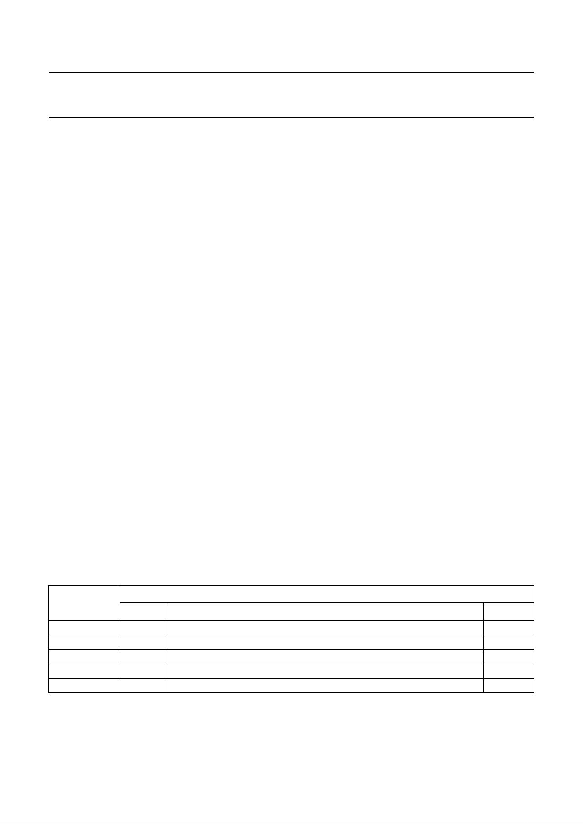
5 BLOCK DIAGRAM
6 PINNING
7 PIN FUNCTIONS
7.1 RS: register select (parallel control)
7.2 R/W: read/write (parallel control)
7.3 E: data bus clock
7.4 DB0 to DB7: data bus
7.5 C1 to C60: column driver outputs
7.6 R1 to R32: row driver outputs
7.7 VLCD: LCD power supply
7.8 V0: VLCD control input
7.9 OSC: oscillator
7.10 SCL: serial clock line
7.11 SDA: serial data line
7.12 SA0: address pin
7.13 T1: test pad
8 FUNCTIONAL DESCRIPTION
8.1 LCD supply voltage generator, PCF2114x and
PCF2116x
8.2 LCD supply voltage generator, PCF2116K
8.3 Character generator ROM (CGROM)
8.4 LCD bias voltage generator
8.5 Oscillator
8.6 External clock
8.7 Power-on reset
8.8 Registers
8.9 Busy Flag
8.10 Address Counter (AC)
8.11 Display data RAM (DDRAM)
8.12 Character generator ROM (CGROM)
8.13 Character generator RAM (CGRAM)
8.14 Cursor control circuit
8.15 Timing generator
8.16 LCD row and column drivers
8.17 Programming MUX 1 : 16 displays with the
PCF2114x
8.18 Programming MUX 1 : 32 displays with the
PCF2114x
8.19 Reset function
9 INSTRUCTIONS
9.1 Clear display
9.2 Return home
9.3 Entry mode set
9.4 Display on/off control
9.5 Cursor/display shift
9.6 Function set
9.7 Set CGRAM address
9.8 Set DDRAM address
9.9 Read busy flag and address
9.10 Write data to CGRAM or DDRAM
9.11 Read data from CGRAM or DDRAM
10 INTERFACE TO MICROCONTROLLER
(PARALLEL INTERFACE)
11 INTERFACE TO MICROCONTROLLER
(I2C-BUS INTERFACE)
11.1 Characteristics of the I2C-bus
11.2 Bit transfer
11.3 START and STOP conditions
11.4 System configuration
11.5 Acknowledge
11.6 I2C-bus protocol
12 LIMITING VALUES
13 HANDLING
14 DC CHARACTERISTICS
15 DC CHARACTERISTICS (PCF2116K)
16 AC CHARACTERISTICS
17 TIMING CHARACTERISTICS
18 APPLICATION INFORMATION
18.1 8-bit operation, 1-line display using internal
reset
18.2 4-bit operation, 1-line display using internal
reset
18.3 8-bit operation, 2-line display
18.4 I2C operation, 1-line display
18.5 Initializing by instruction
19 BONDING PAD LOCATIONS
20 PACKAGE OUTLINE
21 SOLDERING
22 DEFINITIONS
23 LIFE SUPPORT APPLICATIONS
24 PURCHASE OF PHILIPS I2C COMPONENTS
1997 Apr 07 3
Philips Semiconductors Product specification
LCD controller/drivers PCF2116 family
1 FEATURES
• Single chip LCD controller/driver
• 1 or 2-line display of up to 24 characters per line, or
2 or 4 lines of up to 12 characters per line
• 5 × 7 character format plus cursor; 5 × 8 for kana
(Japanese syllabary) and user defined symbols
• On-chip:
– generation of LCD supply voltage (external supply
also possible)
– generation of intermediate LCD bias voltages
– oscillator requires no external components (external
clock also possible)
• Display data RAM: 80 characters
• Character generator ROM: 240 characters
• Character generator RAM: 16 characters
• 4 or 8-bit parallel bus or 2-wire I2C-bus interface
• CMOS/TTL compatible
• 32 row, 60 column outputs
• MUX rates 1 : 32 and 1 : 16
• Uses common 11 code instruction set
• Logic supply voltage range, VDD− VSS: 2.5 to 6 V
• Display supply voltage range, VDD− V
LCD
: 3.5 to 9 V
• Low power consumption
• I2C-bus address: 011101 SA0.
2 APPLICATIONS
• Telecom equipment
• Portable instruments
• Point-of-sale terminals.
3 GENERAL DESCRIPTION
The PCF2116 family of LCD controller/drivers consists of
the PCF2116x, the PCF2114x and the PCF2116K.
The term ‘PCF2116’ is used to refer to all devices for
common information. Specific information is given in
separate paragraphs.
The ‘x’ in ‘PCF2116x’ and ‘PCF2114x’ represents a
specific letter code for a character set in the character
generator ROM (CGROM). The different character sets
currently available are specified by the letters A, C, and G
(see Figs 8 to 10). Other character sets are available on
request.
The PCF2116 is a low-power CMOS LCD controller and
driver, designed to drive a split screen dot matrix LCD
display of 1 or 2 lines by 24 characters or 2 or 4 lines by
12 characters with 5 × 8 dot format. All necessary
functions for the display are provided in a single chip,
including on-chip generation of LCD bias voltages,
resulting in a minimum of external components and lower
system power consumption. The chip contains a character
generator and displays alphanumeric and kana
(Japanese) characters. The PCF2116 interfaces to most
microcontrollers via a 4 or 8-bit bus or via the 2-wire
I
2
C-bus. To allow partial VDD shutdown the ESD protection
system of the SCL and SDA pins does not use a diode
connected to VDD.
The PCF2116K differs from the other members of the
family in that:
• V
LCD/VOP
generation is different (see Section 8.1)
• It is available with character set C only (see Fig.9).
4 ORDERING INFORMATION
Note
1. The letter ‘x’ in the type number represents the letter of the required built-in character set: A, C or G.
TYPE
NUMBER
(1)
PACKAGE
NAME DESCRIPTION VERSION
PCF2116xU/10 − chip on flexible film carrier −
PCF2114xU/10 − chip on flexible film carrier −
PCF2116xU/12 − chip with bumps on flexible film carrier −
PCF2114xU/12 − chip with bumps on flexible film carrier −
PCF2116xHZ LQFP128 plastic low profile quad flat package; 128 leads; body 14 × 20 × 1.4 mm SOT425-1
1997 Apr 07 4
Philips Semiconductors Product specification
LCD controller/drivers PCF2116 family
5 BLOCK DIAGRAM
Fig.1 Block diagram (pin numbers for LQFP128 package).
andbook, full pagewidth
SHIFT REGISTER
32-BIT
MGA797 - 1
V
SS
V
DD
CHARACTER
GENERATOR
RAM
(CGRAM)
16
CHARACTERS
CHARACTER
GENERATOR
ROM
(CGROM)
240
CHARACTERS
CURSOR + DATA CONTROL
5
5
SHIFT REGISTER
5 x 12-bit
60
DATA LATCHES
60
COLUMN DRIVERS
6
BIAS
VOLTAGE
GENERATOR
V
LCD
GENERATOR
93, 95, 97
60
32
ROW DRIVERS
8
DISPLAY DATA RAM
(DDRAM) 80 CHARACTERS
32
84 to 77, 115 to 122
76 to 69, 123 to 128,
1 and 4
ADDRESS
COUNTER (AC)
INSTRUCTION
DECODER
INSTRUCTION
REGISTER (IR)
DATA
REGISTER (DR)
BUSY
FLAG
78 8
I/O BUFFER
8
7
7
8
92
104, 106
109, 112
V
LCD
DISPLAY
ADDRESS
COUNTER
POWER - ON
RESET
TIMING
GENERATOR
OSCILLATOR
7
102
OSC
C1 to C60
R1 to R32
4
105, 103,
98, 96
4
108 110 113
DB0 to DB3 DB4 to DB7 E
RS
R/W
V
0
PCF2116
88
SCL
90
SDA
107
SA0
111
T1
94, 91,
89, 87
68, 65 to 38
35 to 5
1997 Apr 07 5
Philips Semiconductors Product specification
LCD controller/drivers PCF2116 family
6 PINNING
SYMBOL LQFP128 FFC PAD TYPE DESCRIPTION
R31 1 27 O LCD row driver output
n.c. 2 and 3 −−not connected
R32 4 28 O LCD row driver output
C60 to C30 5 to 35 29 to 59 O LCD column driver outputs 60 to 30
n.c. 36 and 37 −−not connected
C29 to C2 38 to 65 60 to 87 O LCD column driver outputs 29to2
n.c. 66 and 67 −−not connected
C1 68 88 O LCD column driver output 1
R24 to R17 69 to 76 89 to 96 O LCD row driver outputs
R8 to R1 77 to 84 97 to 104 O LCD row driver outputs
n.c. 85 and 86 −−not connected
DB7 87 105 I/O 1 bit of 8-bit bidirectional data bus
SCL 88 106 I I
2
C-bus serial clock input
DB6 89 107 I/O 1 bit of 8-bit bidirectional data bus
SDA 90 108 I/O I
2
C-bus serial data input/output
DB5 91 109 I/O 1 bit of 8-bit bidirectional data bus
V
0
92 110 I control input for V
LCD
V
LCD1
93 111 I/O LCD supply voltage input/output 1
DB4 94 112 I/O 1 bit of 8-bit bidirectional data bus
V
LCD2
95 113 I/O LCD supply voltage input/output 2
DB3 96 114 I/O 1 bit of 8-bit bidirectional data bus
V
LCD3
97 115 I/O LCD supply voltage input/output 3
DB2 98 116 I/O 1 bit of 8-bit bidirectional data bus
n.c. 99 to 101 −−not connected
OSC 102 1 I oscillator/external clock input
DB1 103 2 I/O 1 bit of 8-bit bidirectional data bus
V
DD2
104 3 P supply voltage 2
DB0 105 4 I/O 1 bit of 8-bit bidirectional data bus
V
DD1
106 5 P supply voltage 1
SA0 107 6 I I
2
C-bus address pin
E 108 7 I data bus clock input (parallel control)
V
SS1
109 8 P ground (logic) 1
R/
W 110 9 I read/write input (parallel control)
T1 111 10 I test pad (connect to V
SS
)
V
SS2
112 11 P ground (logic) 2
RS 113 12 I register select input (parallel control)
n.c. 114 −−not connected
R9 to R16 115 to 122 13 to 20 O LCD row driver outputs
R25 to R30 123 to 128 21 to 26 O LCD row driver outputs

1997 Apr 07 6
Philips Semiconductors Product specification
LCD controller/drivers PCF2116 family
Fig.2 Pin configuration (LQFP128).
handbook, full pagewidth
MBD451 - 1
1
2
3
4
5
6
7
8
9
10
11
12
13
14
15
16
17
18
19
20
21
22
23
24
25
26
27
28
29
30
102
101
100
99
98
97
96
95
94
93
92
91
90
89
88
87
86
85
84
83
82
81
80
79
78
77
76
75
74
73
394041424344454647
48
495051525354555657585960616263
64
128
127
126
125
124
123
122
121
120
119
118
117
116
115
114
113
112
111
110
109
108
107
106
105
104
103
31
32
33
34
35
36
37
38
72
71
70
69
68
67
66
65
PCF2116
R31
n.c.
n.c.
R32
C60
C59
C58
C57
C56
C55
C54
C53
C52
C51
C50
C49
C48
C47
C46
C45
C44
C43
C42
C41
C40
C39
C38
C37
C36
C35
C34
C33
C32
C31
C30
n.c.
n.c.
C29
OSC
n.c.
n.c.
n.c.
DB2
V
DB3
DB4
V
DB5
SDA
DB6
SCL
DB7
n.c.
n.c.
R1
R2
R3
R4
R5
R6
R7
R8
R17
R18
R19
R20
R21
R22
R23
R24
C1
n.c.
n.c.
C2
LCD3
V
LCD2
V
LCD1
0
C28
C27
C26
C25
C24
C23
C22
C21
C20
C19
C18
C17
C16
C15
C14
C13
C12
C11
C10
C9C8C7C6C5C4C3
R30
R29
R28
R27
R26
R25
R16
R15
R14
R13
R12
R11
R10
R9
n.c.
RS
T1
R/W
E
SA0
DB0VDB1
DD2
V
DD1
V
SS1
V
SS2

1997 Apr 07 7
Philips Semiconductors Product specification
LCD controller/drivers PCF2116 family
7 PIN FUNCTIONS
7.1 RS: register select (parallel control)
RS selects the register to be accessed for read and write
when the device is controlled by the parallel interface.
RS = logic 0 selects the instruction register for write and
the Busy Flag and Address Counter for read. RS = logic 1
selects the data register for both read and write. There is
an internal pull-up on pin RS.
7.2 R/
W: read/write (parallel control)
R/W selects either the read (R/W = logic 1) or write
(R/W = logic 0) operation when control is by the parallel
interface. There is an internal pull-up on this pin.
7.3 E: data bus clock
The E pin is set HIGH to signal the start of a read or write
operation when the device is controlled by the parallel
interface. Data is clocked in or out of the chip on the
negative edge of the clock. Note that this pin must be tied
to logic 0 (V
SS
) when I2C-bus control is used.
7.4 DB0 to DB7: data bus
The bidirectional, 3-state data bus transfers data between
the system controller and the PCF2116. DB7 may be used
as the Busy Flag, signalling that internal operations are not
yet completed. In 4-bit operations the 4 higher order lines
DB4 to DB7 are used; DB0 to DB3 must be left open
circuit. There is an internal pull-up on each of the data
lines. Note that these pins must be left open circuit when
I
2
C-bus control is used.
7.5 C1 to C60: column driver outputs
These pins output the data for pairs of columns.
This arrangement permits optimized chip-on-glass (COG)
layout for 4-line by 12 characters.
7.6 R1 to R32: row driver outputs
These pins output the row select waveforms to the left and
right halves of the display.
7.7 V
LCD
: LCD power supply
Negative power supply for the liquid crystal display.
This may be generated on-chip or supplied externally.
7.8 V
0
: V
LCD
control input
The input level at this pin determines the generated V
LCD
output voltage.
7.9 OSC: oscillator
When the on-chip oscillator is used this pin must be
connected to V
DD
. An external clock signal, if used, is input
at this pin.
7.10 SCL: serial clock line
Input for the I
2
C-bus clock signal.
7.11 SDA: serial data line
Input/output for the I
2
C-bus data line.
7.12 SA0: address pin
The hardware sub-address line is used to program the
device sub-address for 2 different PCF2116s on the same
I
2
C-bus.
7.13 T1: test pad
Must be connected to V
SS
. Not user accessible.
8 FUNCTIONAL DESCRIPTION (see Fig.1)
8.1 LCD supply voltage generator, PCF2114x and
PCF2116x
The on-chip voltage generator is controlled by bit G of the
‘Function set’ instruction and V
0
.
V0 is a high-impedance input and draws no current from
the system power supply. Its range is between VSS and
VDD− 1 V. When V0 is connected to VDD the generator is
switched off and an external voltage must be supplied to
pin V
LCD
. This may be more negative than VSS.
When G = logic 1 the generator produces a negative
voltage at pin V
LCD
, controlled by the input voltage at
pin V0. The LCD operating voltage is given by the
relationship:
VOP= 1.8VDD− V
0
Where:
VOP=VDD− V
LCD
V
LCD=V0
−(0.8VDD)
When G = logic 0, the generated output voltage V
LCD
is
equal to V0 (between VSS and VDD). In this instance:
VOP=VDD− V
0
When V
LCD
is generated on-chip the V
LCD
pin should be
decoupled to VDD with a suitable capacitor. VDD and V
0
must be selected to limit the maximum value of VOPto 9 V.
Figure 3 shows the two generator control characteristics.

1997 Apr 07 8
Philips Semiconductors Product specification
LCD controller/drivers PCF2116 family
8.2 LCD supply voltage generator, PCF2116K
In the PCF2116K version, V0 is connected through an
on-chip resistor (R0) to V
LCD
. Resistor R0 has a nominal
value of 1 MΩ and draws a typical current of 4 µA from the
pin V0. A constant voltage (equal to 1.34VDD) is always
present across R0.
The voltage range of the PCF2116K is between VSS and
VDD− 0.5 V (see Fig.4). When V0 is connected to VDD the
generator is switched off and an external voltage must be
supplied to pin V
LCD
. This may be more negative than VSS.
When G = logic 1 the generator produces a negative
voltage at pin V
LCD
, controlled by the input voltage at
pin V0. The LCD operating voltage is given by the
relationship:
VOP= 2.34VDD− V
0
Where:
VOP=VDD− V
LCD
V
LCD=V0
−(1.34VDD)
When G = logic 0, the generated output voltage V
LCD
is
equal to V0 (between VSS and VDD). In this instance:
VOP=VDD− V
0
8.3 Character generator ROM (CGROM)
The standard character sets A, C and G are available for
the PCF2114x and PCF2116x. Standard character set C is
available for the PCF2116K.
8.4 LCD bias voltage generator
The intermediate bias voltages for the LCD display are
also generated on-chip. This removes the need for an
external resistive bias chain and significantly reduces the
system power consumption. The optimum levels depend
on the multiplex rate and are selected automatically when
the number of lines in the display is defined.
The optimum value of V
OP
depends on the multiplex rate,
the LCD threshold voltage (Vth) and the number of bias
levels and is given by the relationships in Table 1.Using a
5-level bias scheme for 1 : 16 MUX rate allows VOP<5V
for most LCD liquids. The effect on the display contrast is
negligible.
8.5 Oscillator
The on-chip oscillator provides the clock signal for the
display system. No external components are required.
Pin OSC must be connected to VDD.
8.6 External clock
If an external clock is to be used, it must be input at
pin OSC. The resulting display frame frequency is given by
f
frame
=1⁄
2304fosc
. A clock signal must always be present,
otherwise the LCD may be frozen in a DC state.
8.7 Power-on reset
The power-on reset block initializes the chip after
power-on or power failure.
8.8 Registers
The PCF2116 has two 8-bit registers, an Instruction
Register (IR) and a Data Register (DR). The Register
Select signal (RS) determines which register will be
accessed.
The instruction register stores instruction codes such as
‘Display clear’ and ‘Cursor shift’, and address information
for the Display Data RAM (DDRAM) and Character
Generator RAM (CGRAM). The instruction register can be
written to, but not read, by the system controller.
The data register temporarily stores data to be read from
the DDRAM and CGRAM. When reading, data from the
DDRAM or CGRAM corresponding to the address in the
Address Counter is written to the data register prior to
being read by the ‘Read data’ instruction.
8.9 Busy Flag
The Busy Flag indicates the free/busy status of the
PCF2116. Logic 1 indicates that the chip is busy and
further instructions will not be accepted. The Busy Flag is
output to pin DB7 when RS = logic 0 and R/
W = logic 1.
Instructions should only be written after checking that the
Busy Flag is logic 0 or waiting for the required number of
clock cycles.
Table 1 Optimum values for V
OP
MUX RATE
NUMBER OF BIAS
LEVELS
VOP/V
th
DISCRIMINATION
Von/V
off
1 : 16 5 3.67 1.277
1 : 32 6 5.19 1.196
1997 Apr 07 9
Philips Semiconductors Product specification
LCD controller/drivers PCF2116 family
Fig.3 VOP as a function of V0 control characteristics.
a. High-voltage mode VOP= 1.8VDD− V0.
b. Buffer mode VOP=VDD− V0.
MGA798
9
8
7
6
5
4
3.5
0123456
9 V
6 = V
DD
OP(min) DD
V = 0.8 x V 1
V
0
V
OP
5
4
3
2.5
OP(max) DD
V = 1.8 x V
G = 1
MGA799
9
8
7
6
5
4
3.5
0123456
6 = V
DD
V
0
V
OP
5
4
G = 0
1997 Apr 07 10
Philips Semiconductors Product specification
LCD controller/drivers PCF2116 family
Fig.4 VOP as a function of V0 control characteristics (PCF2116K).
a. High-voltage mode VOP= 2.34VDD− V0.
b. Buffer mode VOP=VDD− V0.
MGA799
9
8
7
6
5
4
3.5
0123456
6 = V
DD
V
0
V
OP
5
4
G = 0
MBH667
9
8
7
6
5
4
3.5
0123456
9 V
6
V
0
V
OP
5
4 = V
DD
3
2.5
G = 1
V
OP(min)
= 1.34 × VDD + 0.5

1997 Apr 07 11
Philips Semiconductors Product specification
LCD controller/drivers PCF2116 family
8.10 Address Counter (AC)
The Address Counter assigns addresses to the DDRAM
and CGRAM for reading and writing and is set by the
instructions ‘Set CGRAM address’ and
‘Set DDRAM address’. After a read/write operation the
Address Counter is automatically incremented or
decremented by 1.The Address Counter contents are
output to the bus (DB0 to DB6) when RS = logic 0 and
R/W = logic 1.
8.11 Display data RAM (DDRAM)
The display data RAM stores up to 80 characters of
display data represented by 8-bit character codes.
RAM locations not used for storing display data can be
used as general purpose RAM. The basic
DDRAM-to-display mapping scheme is shown in Fig.5.
With no display shift the characters represented by the
codes in the first 12 or 24 RAM locations starting at
address 00 in line 1 are displayed. Subsequent lines
display data starting at addresses 20, 40, or 60 Hex.
Figs 6 and 7 show the DDRAM-to-display mapping
principle when the display is shifted.
The address range for a 1-line display is 00 to 4F; for a
2-line display from 00 to 27 (line 1) and 40 to 67 (line 2);
for a 4-line display from 00 to 13, 20 to 33, 40 to 53 and
60 to 73 for lines 1, 2, 3 and 4 respectively.
For 2 and 4-line displays the end address of one line and
the start address of the next line are not consecutive.
When the display is shifted each line wraps around
independently of the others (Figs 6 and 7).
When data is written into the DDRAM wrap-around occurs
from 4F to 00 in 1-line mode and from 27 to 40 and
67 to 00 in 2-line mode; from 13 to 20, 33 to 40, 53 to 60
and 73 to 00 in 4-line mode.
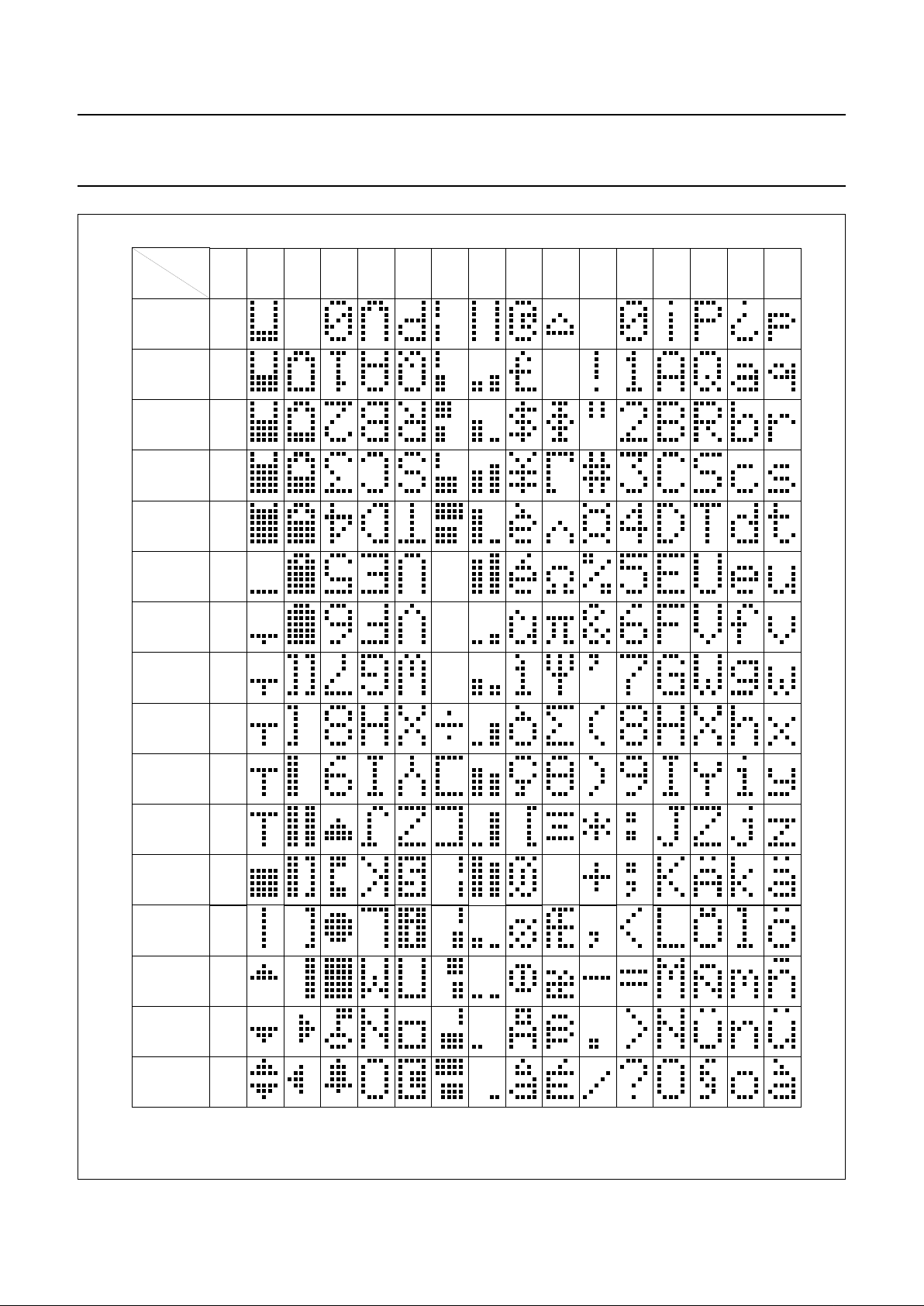
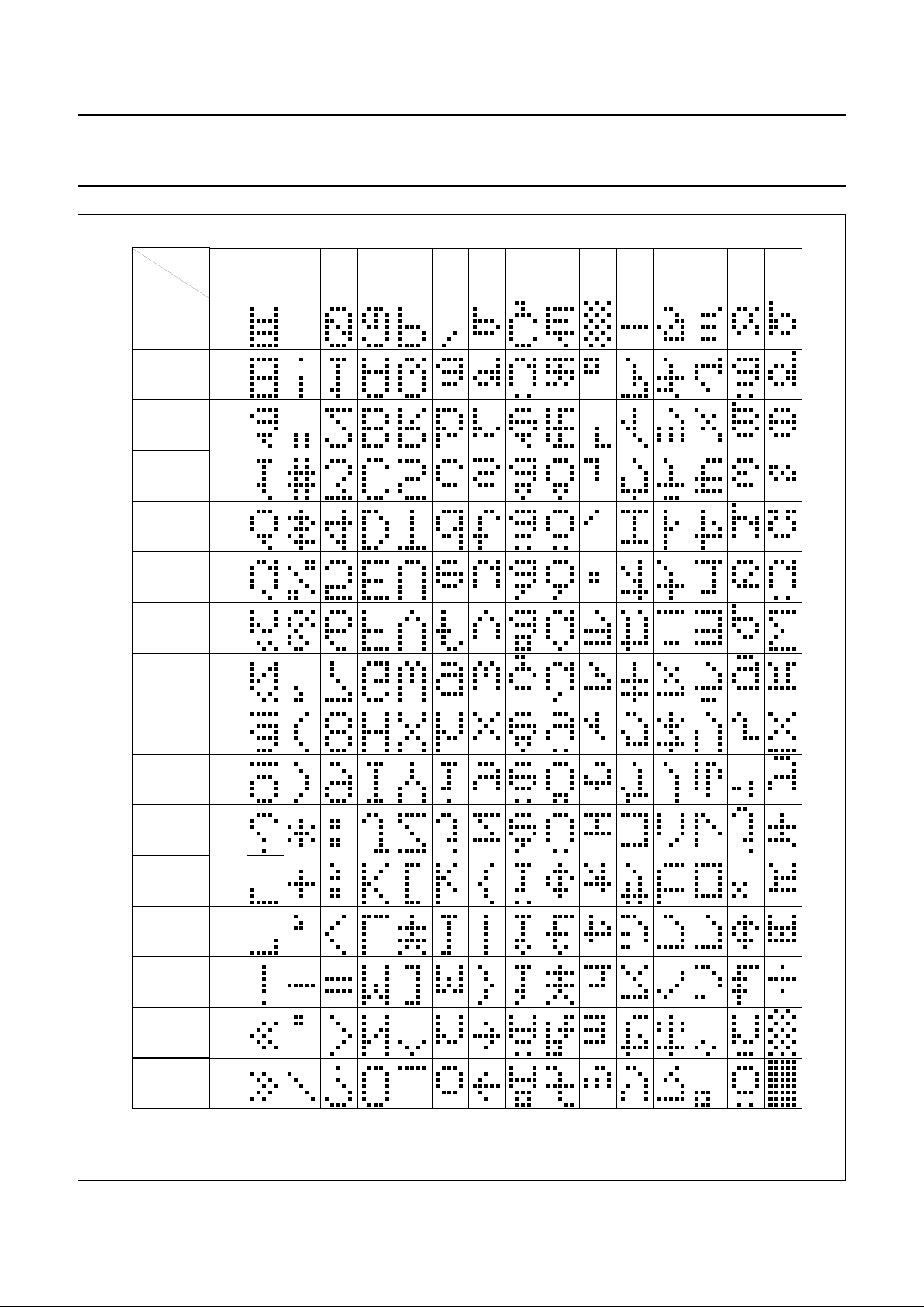
8.12 Character generator ROM (CGROM)
The character generator ROM generates 240 character
patterns in 5 × 8 dot format from 8-bit character codes.
Figures 8 to 10 show the character sets currently
available.
8.13 Character generator RAM (CGRAM)
Up to 16 user-defined characters may be stored in the
character generator RAM. The CGROM and CGRAM use
a common address space, of which the first column is
reserved for the CGRAM (see Fig.8). Figure 11 shows the
addressing principle for the CGRAM.
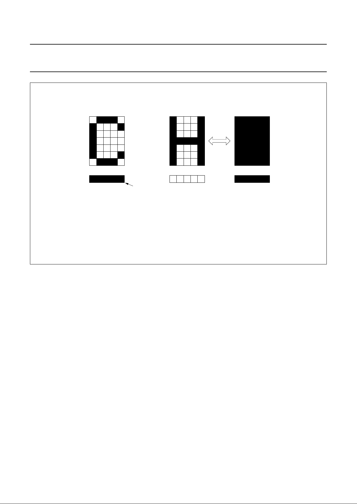
8.14 Cursor control circuit
The cursor control circuit generates the cursor (underline
and/or character blink as shown in Fig.12) at the DDRAM
address contained in the Address Counter. When the
Address Counter contains the CGRAM address the cursor
will be inhibited.
8.15 Timing generator
The timing generator produces the various signals
required to drive the internal circuitry. Internal chip
operation is not disturbed by operations on the data buses.
8.16 LCD row and column drivers
The PCF2116 contains 32 row and 60 column drivers,
which connect the appropriate LCD bias voltages in
sequence to the display, in accordance with the data to be
displayed. The bias voltages and the timing are selected
automatically when the number of lines in the display is
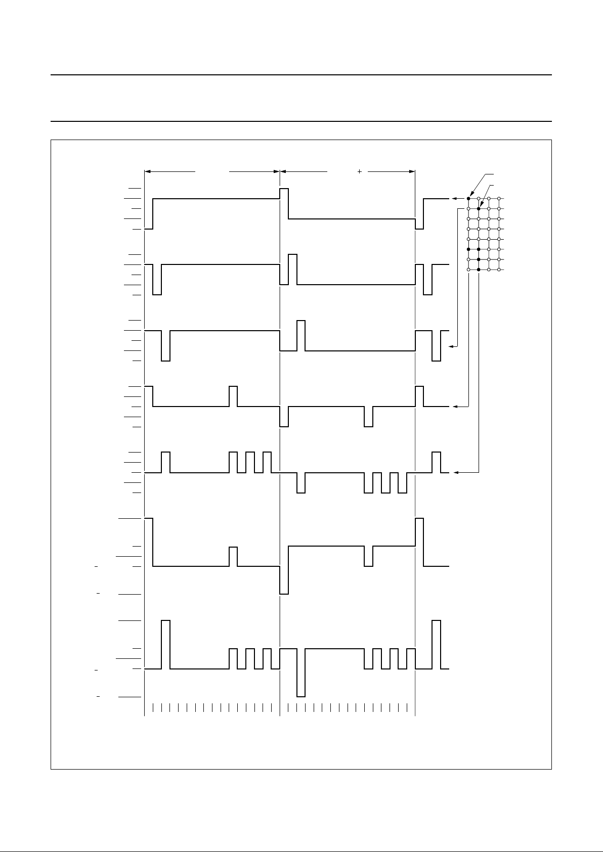
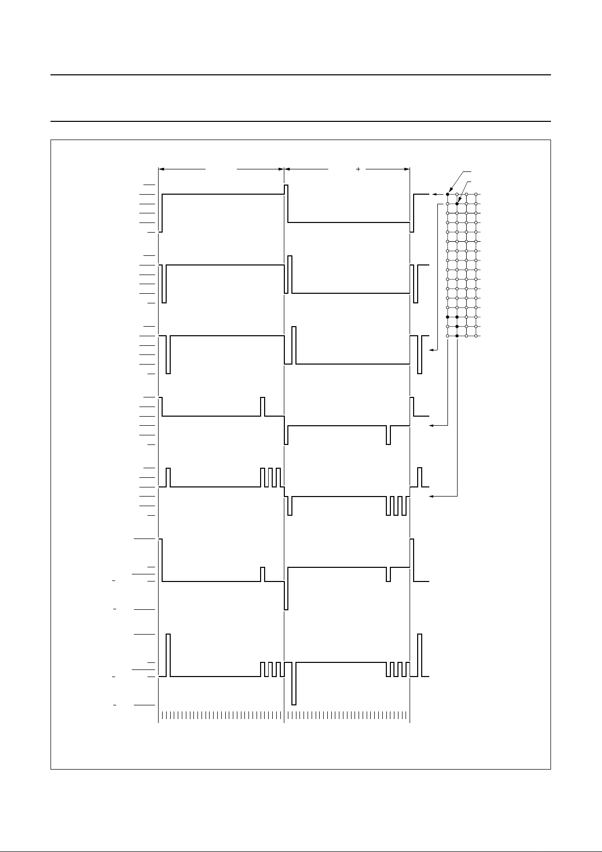
selected. Figures 13 and 14 show typical waveforms.
In 1-line mode (1 : 16) the row outputs are driven in pairs:
R1/R17, R2/R18 for example. This allows the output pairs
to be connected in parallel, providing greater drive
capability.
Unused outputs should be left unconnected.
1997 Apr 07 12
Philips Semiconductors Product specification
LCD controller/drivers PCF2116 family
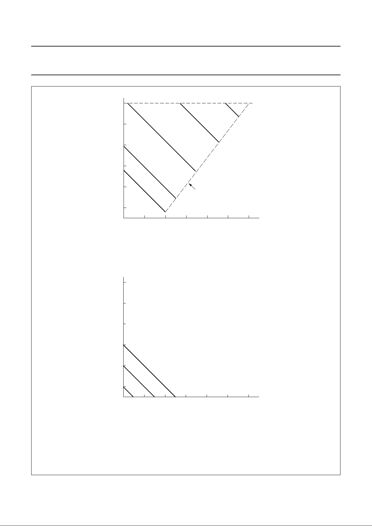
Fig.5 DDRAM-to-display mapping; no shift.
handbook, 4 columns
12345 222324
00 01 02 03 04 15 16 17 18 19 4C 4D 4E 4F
non-displayed DDRAM addresses
Display
Position
(decimal)
DDRAM
Address
(hex)
1-line display
64 65 66 6740 41 42 43 44 55 56 57 58 59
00 01 02 03 04 15 16 17 18 19
24 25 26 27
non-displayed DDRAM address
DDRAM
(hex)
Address
2-line display
line 1
line 2
MLA792
handbook, 4 columns
123456789101112
non-displayed DDRAM addresses
DDRAM
Address
(hex)
4 line display
00 01 02 03 04 05 06 07 08 09 0A 0B 0C 0D 0E 0F 10 11 12 13
20 21 22 23 24 25 26 27 28 29 2A 2B 2C 2D 2E 2F 30 31 32 33
40 41 42 43 44 45 46 47 48 49 4A 4B 4C 4D 4E 4F 50 51 52 53
60 61 62 63 64 65 66 67 68 69 6A 6B 6C 6D 6E 6F 70 71 72 73
line 1
line 2
line 3
line 4
MLA793
1997 Apr 07 13
Philips Semiconductors Product specification
LCD controller/drivers PCF2116 family
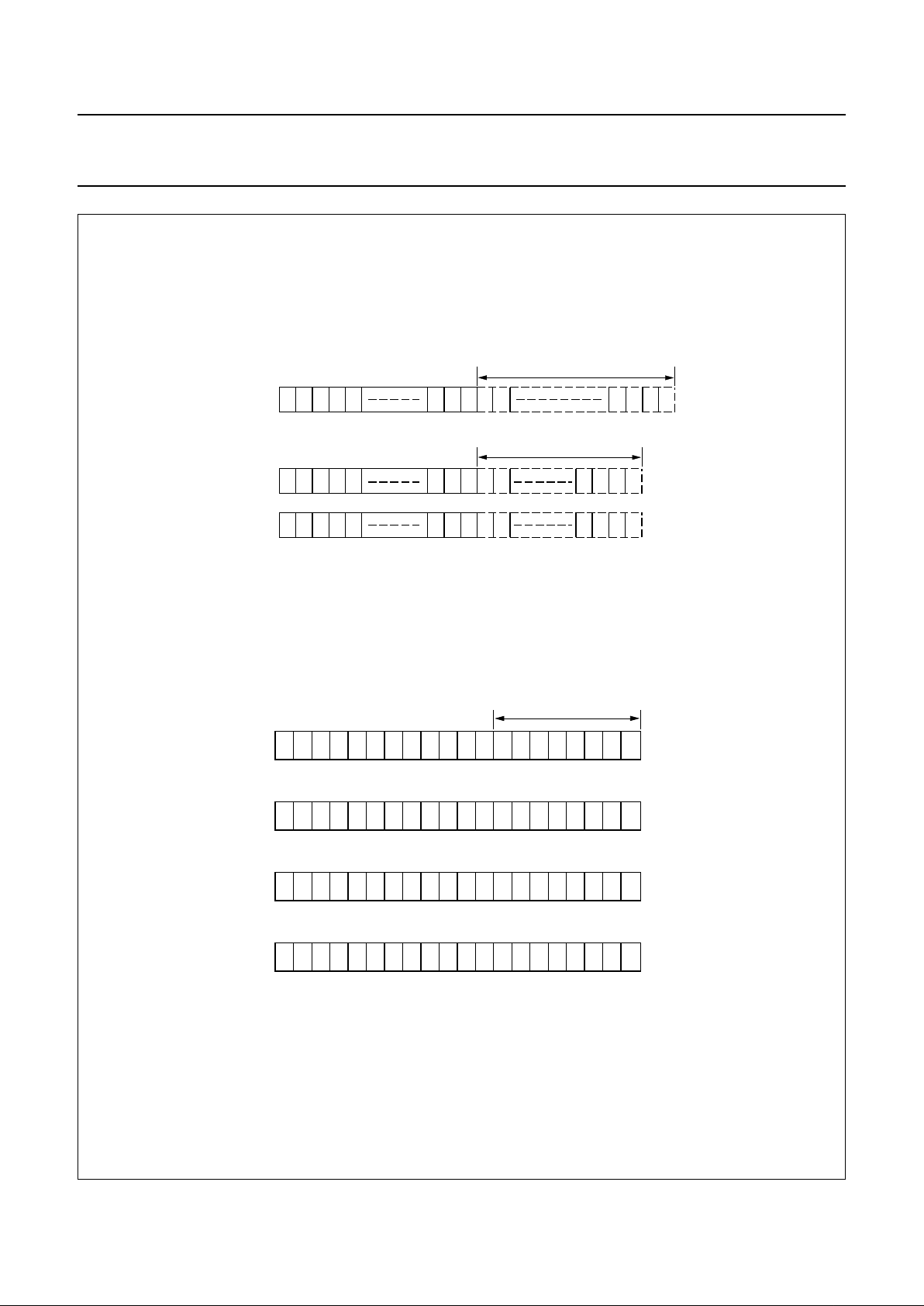
Fig.6 DDRAM-to-display mappi7ng; right shift.
27 00 01 02 03
67 40 41 42 43
14 15 16
54 55 56
DDRAM
Address
(hex)
line 1
line 2
2-line display
1 2 3 4 5 22 23 24
4F 00 01 02 03 14 15 16
Display
Position
(decimal)
DDRAM
Address
(hex)
1-line display
MLA802
13 01 02 03 04 05 06 07 08 09 0A
20 21 22 23 24 25 26 27 28 29 2A33
40 41 42 43 44 45 46 47 48 49 4A53
60 61 62 63 64 65 66 67 68 69 6A73
123456789101112
DDRAM
Address
(hex)
line 1
line 2
line 3
line 4
4-line display
00
MLA803
Fig.7 DDRAM-to-display mapping; left shift.
1 2 3 4 5 22 23 24
0501 02 03 04
16 17 18
41 42 43 44 45 56 57 58
0501 02 03 04
16 17 18
Display
Position
(decimal)
DDRAM
Address
(hex)
DDRAM
Address
(hex)
line 1
line 2
1-line display
2-line display
MLA815
01 02 03 04 05 06 07 08 09 0A 0B 0C
21 22 23 24 25 26 27 28 29 2A 2B 2C
41 42 43 44 45 46 47 48 49 4A 4B 4C
61 62 63 64 65 66 67 68 69 6A 6B 6C
123456789101112
DDRAM
Address
(hex)
line 1
line 2
line 3
line 4
4-line display
MLA816
1997 Apr 07 14
Philips Semiconductors Product specification
LCD controller/drivers PCF2116 family
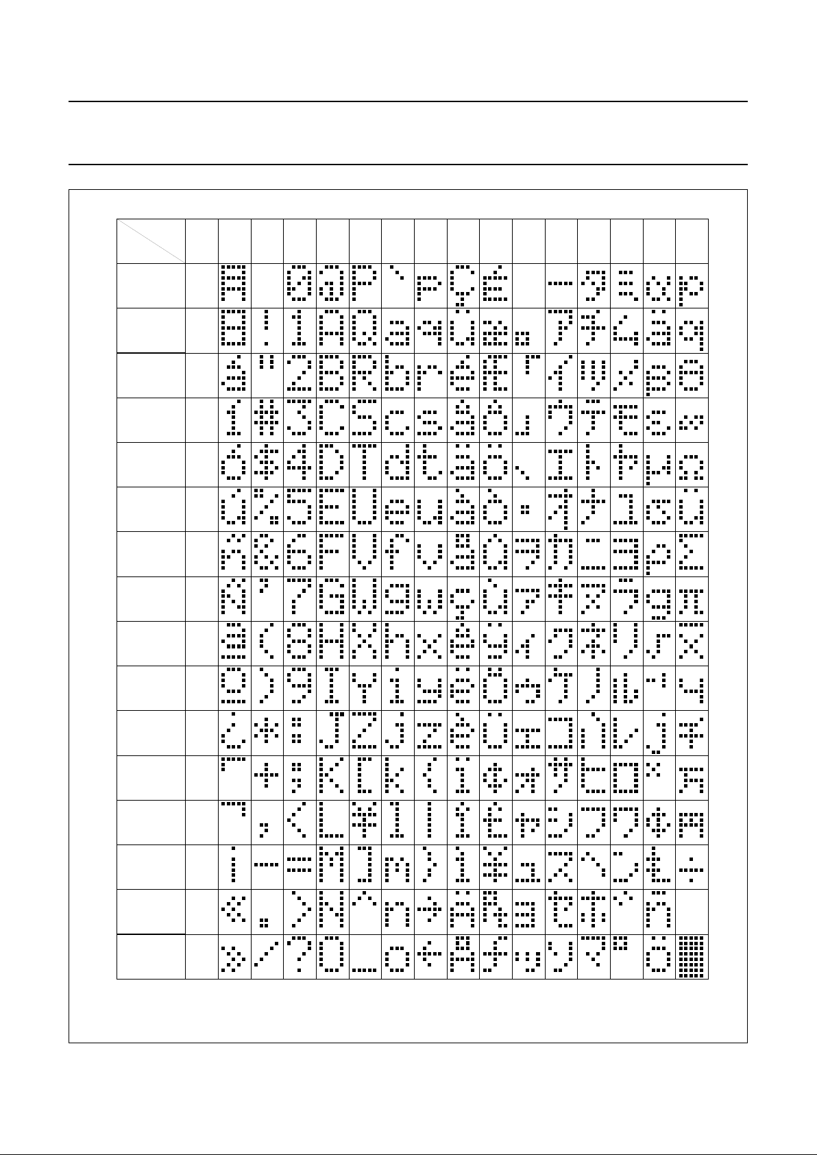
Fig.8 Character set ‘A’ in CGROM: PCF2116A; PCF2114A.
handbook, full pagewidth
MLB245 - 1
0000 0001 0010 0011 0100 0101 0110 0111 1000 1001 1010 1011 1100 1101 1110 1111
upper
4 bits
lower
6 bits
xxxx 0000
xxxx 0001
xxxx 0010
xxxx 0011
xxxx 0100
xxxx 0101
xxxx 0110
xxxx 0111
xxxx 1000
xxxx 1001
xxxx 1010
xxxx 1011
xxxx 1100
xxxx 1101
xxxx 1110
xxxx 1111 16
15
14
13
12
11
10
9
8
7
6
5
4
3
2
1
1997 Apr 07 15
Philips Semiconductors Product specification
LCD controller/drivers PCF2116 family
Fig.9 Character set ‘C’ in CGROM: PCF2116C; PCF2114C.
handbook, full pagewidth
MLB895
0000 0001 0010 0011 0100 0101 0110 0111 1000 1001 1010 1011 1100 1101 1110 1111
upper
4 bits
lower
4 bits
xxxx 0000
xxxx 0001
xxxx 0010
xxxx 0011
xxxx 0100
xxxx 0101
xxxx 0110
xxxx 0111
xxxx 1000
xxxx 1001
xxxx 1010
xxxx 1011
xxxx 1100
xxxx 1101
xxxx 1110
xxxx 1111 16
15
14
13
12
11
10
9
8
7
6
5
4
3
2
CG
RAM 1
1997 Apr 07 16
Philips Semiconductors Product specification
LCD controller/drivers PCF2116 family
Fig.10 Character set ‘G’ in CGROM: PCF2116G; PCF2114G.
handbook, full pagewidth
MLB896
0000 0001 0010 0011 0100 0101 0110 0111 1000 1001 1010 1011 1100 1101 1110 1111
upper
4 bits
lower
6 bits
xxxx 0000
xxxx 0001
xxxx 0010
xxxx 0011
xxxx 0100
xxxx 0101
xxxx 0110
xxxx 0111
xxxx 1000
xxxx 1001
xxxx 1010
xxxx 1011
xxxx 1100
xxxx 1101
xxxx 1110
xxxx 1111 16
15
14
13
12
11
10
9
8
7
6
5
4
3
2
CG
RAM 1
1997 Apr 07 17
Philips Semiconductors Product specification
LCD controller/drivers PCF2116 family
Fig.11 Relationship between CGRAM addresses and data and display patterns.
handbook, full pagewidth
MGA800 - 1
76543210 6543210 43210
higher
order
bits
lower
order
bits
lower
order
bits
higher
order
bits
lower
order
bits
higher
order
bits
00000000 0000000 0
001 000
010 000
011 0
100 0 00
101 00 0
110 000
111 00000
000 000
001 0 0 0
010
00 00011
100
101 00 00
110 00 00
111 00000
001
00000001 0001
00000010
00001111
00001111
00001111
00001111
010 0000
100
101
110
1
1
1
1
1
1
1
1
1
1
1
1
1
1
1
1
111
character codes
(DDRAM data)
CGRAM
address
character patterns
(CGRAM data)
character
pattern
example 1
cursor
position
character
pattern
example 2
Character code bits 0to 3 correspond to CGRAM address bits 3 to 6.
CGRAM address bits 0 to 2 designate character pattern line position. The 8th line is the cursor position and display is performed by logical OR with
the cursor. Data in the 8th line will appear in the cursor position.
Character pattern column positions correspond to CGRAM data bits 0 to 4, as shown in Fig.11 (bit 4 being at the left end).
As shown in Figs 8 and 11, CGRAM character patterns are selected when character code bits 4 to 7 are all logic 0. CGRAM data = logic 1
corresponds to selection for display.
Only bits 0 to 5 of the CGRAM address are set by the ‘Set CGRAM address’ instruction. Bit 6 can be set using the ‘Set DDRAM address’ instruction
or by using the auto-increment feature during CGRAM write. All bits 0 to 6 can be read using the ‘Read busy flag and address’ instruction.
1997 Apr 07 18
Philips Semiconductors Product specification
LCD controller/drivers PCF2116 family
Fig.12 Cursor and blink display examples.
MGA801
cursor
5 x 7 dot character font alternating display
cursor display example blink display example
1997 Apr 07 19
Philips Semiconductors Product specification
LCD controller/drivers PCF2116 family
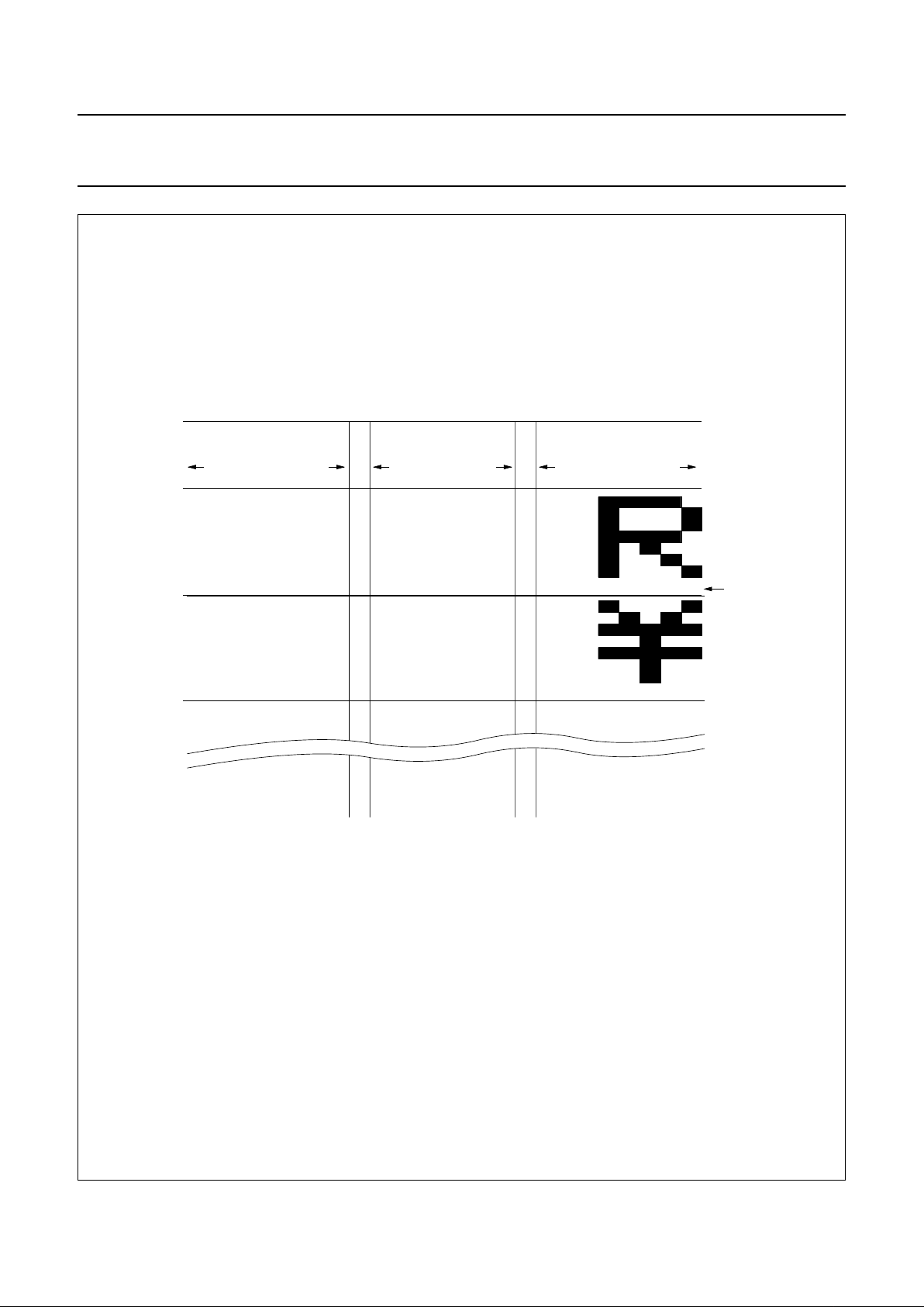
Fig.13 Typical LCD waveforms; 1-line mode.
handbook, full pagewidth
MGA802 - 1
V
DD
V
2
V
V
5
LCD
ROW 1
COL 1
state 1 (ON)
state 2 (ON)
0.25 V
OP
0 V
state 1
1-line display
(1:16)
frame n 1frame n
ROW 9
ROW 2
COL 2
state 2
123 16123 16
34
V /V
V
DD
V
2
V
V
5
LCD
34
V /V
V
DD
V
2
V
V
5
LCD
34
V /V
V
DD
V
2
V
V
5
LCD
34
V /V
V
DD
V
2
V
V
5
LCD
3
4
V /V
0.25 V
OP
0.25 V
OP
0 V
0.25 V
OP
V
OP
V
OP
V
OP
V
OP
1997 Apr 07 20
Philips Semiconductors Product specification
LCD controller/drivers PCF2116 family
Fig.14 Typical LCD waveforms; 2-line mode.
handbook, full pagewidth
MGA803 - 1
V
DD
V
2
V
V
V
V
3
4
5
LCD
ROW 1
V
DD
V
2
V
V
V
V
3
4
5
LCD
V
DD
V
2
V
V
V
V
3
4
5
LCD
COL 1
V
DD
V
2
V
V
V
V
3
4
5
LCD
state 1 (ON)
state 2 (ON)
0.15 V
OP
0 V
V
OP
V
OP
V
OP
state 1
2-line display
(1:32)
frame n 1
frame n
ROW 9
ROW 2
COL 2
V
DD
V
2
V
V
V
V
3
4
5
LCD
0.15 V
OP
0.15 V
OP
0 V
0.15 V
OP
V
OP
state 2
123 3212 3 32
 Loading...