

Philips pcd5042 DATASHEETS

INTEGRATED CIRCUITS
DATA SH EET
PCD5042
DECT burst mode controller
Objective specification
File under Integrated Circuits, IC17
1996 Oct 31

Philips Semiconductors Objective specification
DECT burst mode controller PCD5042
CONTENTS
FEATURES
2 GENERAL DESCRIPTION
3 ORDERING INFORMATION
4 BLOCK DIAGRAM
5 PINNING
6 FUNCTIONAL DESCRIPTION
6.1 Internal bus and data memory
6.1.1 Internal Bus
6.1.2 Data Memory
6.2 Clock generation and correction
6.3 Programmable communication controller and
program memory
6.3.1 PCC
6.3.2 PCC functions
6.4 Speech interface
6.4.1 12-slot mode
6.4.2 32-slot mode
6.4.3 Muting
6.4.4 Local call
6.5 RF interface
6.5.1 Serial receiver
6.5.2 Serial transmitter
6.5.3 Seamless handover
6.5.4 RF control signals
6.5.5 Synthesizer programming
6.5.6 RSSI measurement
6.5.7 Local call switching
6.5.8 Data synchronization
6.5.9 Ciphering machine
6.5.10 Comparator/data slicer on PCD5042HZ
6.6 Microcontroller Interface
6.6.1 Function of the microcontroller interface
6.6.2 Microcontroller interrupts
6.6.3 Watchdog
6.6.4 Power-down
6.7 Survey of registers
7 LIMITING VALUES
8 CHARACTERISTICS
9 PACKAGE OUTLINES
10 SOLDERING
10.1 Introduction
10.2 Reflow soldering
10.3 Wave soldering
10.4 Repairing soldered joints
11 DEFINITIONS
12 LIFE SUPPORT APPLICATIONS
1996 Oct 31 2

Philips Semiconductors Objective specification
DECT burst mode controller PCD5042
1 FEATURES
• On-chip pre-programmed Communication Controller
with embedded firmware for implementation of Traffic
Bearer Control (TBC), MAC message handling,
scanning, and control of the device’s other functional
units.
• Fixed Part (FP) modes
• TDMA frame (de)multiplexing
• Encryption
• Scrambling
• CRC generation and checking
• Beacon transmission control (by P00 packets)
• On-chip comparator for receive data slicer function (only
available in the LQFP80 package)
• Switches up to12 active speech channels from speech
interface to 1152 kbits/s. radio interface, and vice versa
• Dual channel speech/data capability
• RSSI measurement, with on-chip 6-bits peak/hold
detector
• Local call switching for up to 6 internal calls on RF
side/local call switching on speech side.
• Quality control report
• Digital Phase Locked Loop (DPLL)
• Synchronization (handset to active bearer, base station
to cluster of RFPs)
• Seamless handover procedure
• Fast (hardware) and slow (software) mute function
• 1 kbyte extended RAM memory
• On-chip crystal oscillator (13.824 MHz)
• Programmable microcontroller clock frequency
• Programmable interrupts
• Watchdog with two programmable time-outs
• Low power consumption in standby mode
• Low supply voltage (2.7 to 5.5 V)
• SACMOS technology.
2 GENERAL DESCRIPTION
The PCD5042 DECT Burst Mode Controller (BMC) is a
custom IC that performs the DECT Physical Layer and
MAC Layer time-critical functions, for use in DECT base
station products which comply with the following
standards:
• DECT CI part 2: Physical layer (DE/RES 3001-2)
• DECT CI part 3 : Medium Access Control layer
(DE/RES 3001-3)
• DECT CI part 7: Security features for DECT
(DE/RES 3001-7)
• DECT CI part 9: Public Access Profile
(DE/RES 3001-9).
The PCD5042 has interfaces to:
• Up to 4 ADPCM CODECs in a simple base station (with
up to 4 analogue lines) without glue logic
• n x 64 kbits/s highway, where n=1to32, for systems
requiring more than 4 connections to the network
• A radio transceiver; the interface is fully decoded, and
includes power-down signals
• An external microcontroller.
The PCD5042 is designed to be connected to an ADPCM
CODEC (Philips’ PCD5032, for example) and an
80C51-type microcontroller. Other microcontrollers (e.g.
68000) and CODECs can also be supported.
3 ORDERING INFORMATION
TYPE
NUMBER
PCD5042H QFP64
PCD5042HZ
1996 Oct 31 3
NAME DESCRIPTION VERSION
plastic quad flat package; 64 leads (lead length 1.95 mm); body
14 × 20 × 2.8 mm
LQFP80 plastic low profile quad flat package; 80 leads; body 12 × 12 × 1.4 mm
PACKAGE
SOT319-2
SOT315-1
Philips Semiconductors Objective specification
DECT burst mode controller PCD5042
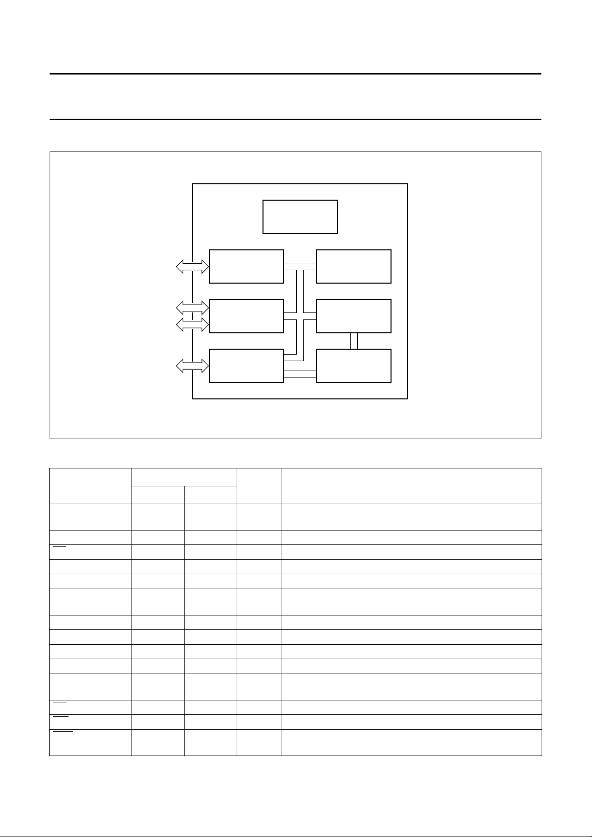
4 BLOCK DIAGRAM
handbook, full pagewidth
PCD5042
to CODEC/
Highway
DECT
BURST MODE
CONTROLLER
SPEECH
INTERFACE
TIMING, CONTROL,
CLOCK
GENERATION
internal
bus
DATA MEMORY
2 kbyte RAM
3-wire synthesizer
interface
Rx/Tx data
8051/68000
interface
RF INTERFACE
MICROCONTROLLER
INTERFACE
PROGRAMMABLE
COMMUNICATION
CONTROLLER (PCC)
PCC
PROGRAM MEMORY
4 kbyte ROM
MBH741
Fig.1 Block diagram.
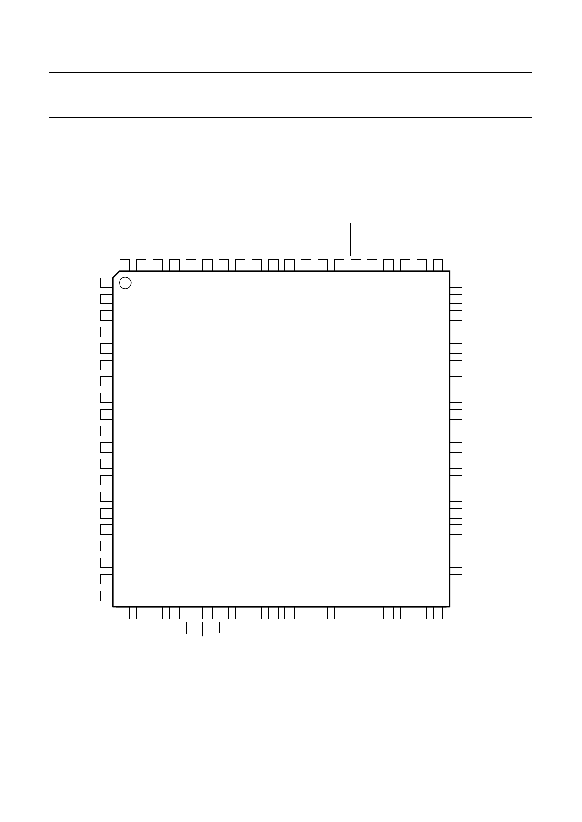
5 PINNING (see Figs 2 and 3)
SYMBOL
PIN
QFP64 LQFP80
AD0 to AD7 1 to 8 80, 1, and
(1)
(2)
TYPE
I/O address/Data bus
DESCRIPTION
3to7
ALE 9 9 I address latch enable
CS 10 11 I chip select (active LOW)
A8 to A10 13 to 11 14 to 12 I address bus
V
DD1
PROC_CLK 15 16 O microcontroller clock; programmable from f
V
SS1
14 15 P positive supply 1
where f
is the crystal oscillator frequency
CLK
16 17 P negative supply 1
CLK
/64 to f
XTAL1 17 20 I crystal oscillator input
XTAL2 18 21 O crystal oscillator output
V
SS2
19 22 P negative supply
RESET_OUT 20 23 O watchdog timer output; intended to reset the external
microcontroller when expired
RD 21 24 I read (active LOW)
WR 22 25 I write (active LOW)
RDY 23 26 O ready signal (active LOW), to initiate wait states in the
microcontroller (open drain)
CLK
,
1996 Oct 31 4
Philips Semiconductors Objective specification
DECT burst mode controller PCD5042
SYMBOL
PIN
QFP64 LQFP80
(1)
TYPE
(2)
DESCRIPTION
INT 24 27 O interrupt (active LOW)
CLK100 25 29 O 100 Hz frame timer
V
SS3
26 31 P negative supply 3
DO 27 32 O 3-state data output on the speech interface
FS3 − 33 I/O 8 kHz framing signal to ADPCM CODEC 1 output, for simple
base + handset, otherwise 8 kHz framing input
FS1 28 34 I/O 8 kHz framing signal to ADPCM CODEC 1 output, for simple
base + handset, otherwise 8 kHz framing input
FS4 − 35 I/O 8 kHz framing signal to ADPCM CODEC 1 output, for simple
base + handset, otherwise 8 kHz framing input
FS2 29 36 O 8 kHz framing signal to ADPCM CODEC 2 in the base station
mode
DI 30 37 I data input on the speech interface
DCK 31 38 O simple base + handset; 1152 kHz data clock (output),
otherwise 2048 kHz data clock (input) signal
CLK3 32 39 O 3.456 MHz clock (nominal value, used to adjust system
timing)
ANT_SW 33 40 O selects one of two antennas
T_ENABLE 34 41 O Transmitter Enable (active LOW)
T_POWER_RMP 35 43 O Transmitter Power Ramp control
RMT_STAT 36 44 I serial 8-bit data can be read in for each slot; REMote radio
SYNTH_LOCK 37 45 I lock indication from synthesizer
V
SS4
38 46 P negative supply 4
REF_CLK 39 47 O reference frequency for the synthesizer, i.e. the crystal
V
DD2
oscillator clock f
40 48 P positive supply 2
CLK
S_ENABLE 41 49 O synthesizer enable
S_CLK 42 51 O clock signal, to be used with S_DATA
S_DATA 43 52 O serial data to the synthesizer
S_POWER_DWN 44 53 O synthesizer power-down control
VCO_BND_SW 45 54 O VCO bandswitch control signal
1200 HZ 46 55 O control signal for dual synthesizer schemes
T_DATA 47 56 O serial output data to transmitter
SET_OFF_IN 48 57 I switches off the crystal oscillator, and prevents all RF signals
from becoming active
TEST1 49 58 I selects various test modes.; normal operation set to 0
RSSI_AN 50 60 I analog signal (for basic DECT systems), peak signal strength
measured after a lowpass filter
TEST2 51 − I selects various test modes; normal operation set to 0
TEST3 52 61 I selects various test modes; normal operation set to 0
R_DATA 53 63 I receive data
1996 Oct 31 5
Philips Semiconductors Objective specification
DECT burst mode controller PCD5042
SYMBOL
PIN
QFP64 LQFP80
(1)
TYPE
(2)
DESCRIPTION
R_ENABLE 54 64 O receiver enable (active LOW)
R_POWER_DWN 55 65 O receiver power-down
COMP_NE − 66 I digital input comparator not_enable (active LOW)
SLICE_CTR 56 67 O slice time constant control
COMP_OUT − 68 O digital comparator output
V
V
DD3
SS5
57 69 P positive supply 3
58 70 P negative supply 5
COMP_INM − 71 I analog comparator input negative
V
REF
59 72 I reference input for the A/D converter
COMP_INP − 73 I analog input positive
V
DD(RAM)
60 74 P power supply for data RAM
SYNCPORT 61 76 I/O in the base station the signal is the SYNCPORT
RESET 62 77 I BMC master reset signal
MEM_SEL 63 78 I selects PCC program memory at microcontroller interface
EN_WATCHDOG 64 79 I enable watchdog input; when HIGH, the watchdog timer of
the BMC is enabled
Notes
1. Un-referenced pins for the LQFP80 package are not connected. FS3, FS4 and the comparator signals are only
available in the LQFP80 package.
2. All signals which are input or I/O, and which can be floating, need to be pulled up to VDD or down to VSS in order to
protect the device against cross-currents. Exceptions are VREF and RSSI_AN, which do not have to be protected.
1996 Oct 31 6
Philips Semiconductors Objective specification
DECT burst mode controller PCD5042
handbook, full pagewidth
AD0
AD1
AD2
AD3
AD4
AD5
AD6
AD7
ALE
CSN
AD10
AD9
AD8
V
DD1
PROC_CLK
V
SS1
XTAL1
XTAL2
V
SS2
1
2
3
4
5
6
7
8
9
10
11
12
13
14
15
16
17
18
19
EN_WATCHDOG
MEM_SEL
MEM_RESET
64
63
62
DD(RAM)
SYNCPORT
V
61
60
PCD5042H
VREF
59
SS5VDD3
V
58
57
SLICE_CTR
R_POWER_DWN
56
55
R_ENABLE
R_DATA
54
53
TEST3
52
51
50
49
48
47
46
45
44
43
42
41
40
39
38
37
36
35
34
33
TEST2
RSSI_AN
TEST1
SET_OFF_IN
T_DATA
1200_Hz
VCO_BND_SW
S_POWER_DWN
S_DATA
S_CLK
S_ENABLE
V
DD2
REF_CLK
V
SS4
SYNTH_LOCK
RMT_STAT
T_POWER_RMP
T_ENABLE
ANT_SW
20
21
22
23
24
25
RD
WR
RESET_OUT
RDY
INT
CLK100
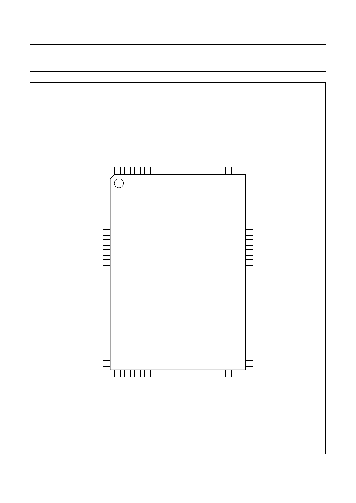
Fig.2 Pin configuration, PCD5042H (QFP64 package).
1996 Oct 31 7
26
SS3
V
27
DO
28
FS1
29
FS2
30
31
32
DCK
MBH743
CLK3
DI
Philips Semiconductors Objective specification
DECT burst mode controller PCD5042
handbook, full pagewidth
AD1
n.c.
AD2
AD3
AD4
AD5
AD6
AD7
ALE
n.c.
CSN
AD10
AD9
AD8
V
DD1
PROC_CLK
V
SS1
n.c.
n.c.
XTAL1
AD0
EN_WATCHDOG
MEM_SEL
RESET
SYNCPORT
80
79
78
77
76
1
2
3
4
5
6
7
8
9
10
n.c.
75
DD(RAM)
V
COMP_INP
74
73
VREF
72
SS5VDD3
V
COMP_INN
71
70
69
SLICE_CTR
COMP_OUT
68
67
R_POWER_DWN
COMP_NE
66
65
R_ENABLE
R_DATA
64
63
TEST3
62
TEST2
61
60
59
58
57
56
55
54
53
52
51
RSSI_AN
n.c.
TEST1
SET_OFF_IN
T_DATA
1200_Hz
VCO_BND_SW
S_POWER_DWN
S_DATA
S_CLK
PCD5042HZ
11
12
13
14
15
16
17
18
19
20
50
n.c.
S_ENABLE
49
V
48
DD2
REF_CLK
47
V
SS4
46
SYNTH_LOCK
45
RMT_STAT
44
T_POWER_RMP
43
42
n.c.
T_ENABLE
41
21
22
23
24
25
26
27
28
29
30
XTAL2
SS2
V
RD
WR
RESET_OUT
RDY
INT
n.c.
n.c.
CLK100
Fig.3 Pin configuration, PCD5042HZ (LQFP80 package).
1996 Oct 31 8
31
SS3
V
32
DO
33
FS3
34
FS1
35
FS4
36
FS2
37
38
39
40
MBH745
DI
DCK
CLK3
ANT_SW

Philips Semiconductors Objective specification
DECT burst mode controller PCD5042
6 FUNCTIONAL DESCRIPTION (see Fig.1) The PCD5042 has dedicated hardware blocks containing
logic for time-critical functions requiring bit or byte-time
accuracy. Other functions requiring only slot-time
accuracy are performed by software in the
Preprogrammed Communication Controller (PCC). This
approach offers maximum flexibility during prototyping.
6.1 Internal bus and data memory
6.1.1 I
NTERNAL BUS
The function of the internal bus is:
• To provide access for all functional blocks to the
common data memory
• To provide access for the microcontroller-interface and
the PCC to all other functional blocks.
All functional blocks (speech-interface, RF-interface,
microcontroller-interface and PCC) can autonomously use
the internal bus to communicate with the common data
memory.
A bus controller is used to handle the bus priority
mechanism. When several blocks request access
simultaneously, the request with the highest priority is
handled first.
6.1.2 D
ATA MEMORY
A large part of the data memory is used for the bit rate
adaptation between the DECT radio interface and the
speech interface. The data memory also acts as the main
communication interface between the external
microprocessor and the PCC.
6.2 Clock generation and correction (see Fig.4)
The device has an on-chip 13.824 MHz crystal oscillator.
From this source, a few frequencies are derived for internal
and external use. Frequencies generated for external use
are:
• 13.824 MHz for the synthesizer reference
(pin REF_CLK). This output is only provided if the
synthesizer power-down control (output on
pin S_POWER_DWN) is not selected.
• 0.144 to 13.824 MHz for the microcontroller clock
(pin PROC_CLK)
• 3.456 MHz for the ADPCM CODEC (pin CLK3)
• 1200 Hz (pin 1200_HZ) for dual synthesizer switching
• 100 Hz (pin CLK100) indicates start of frame.
Nominally, the frequency on pin CLK3 is 3.456 MHz. This
frequency is obtained by dividing the crystal frequency by
4. Sometimes, the crystal frequency will be divided by 3
or by 5, to synchronize the combination of the ADPCM
CODEC and the device to an external source. External
synchronization for base station applications is achieved
as follows:
• Master base station. The master base station provides
a 100 Hz signal to slave base stations on pin
SYNCPORT. If the PCD5042 is connected to a digital
interface (32-slot mode speech interface), the external
synchronization will be done on the incoming 8 kHz
signal. If it is connected to an analog line (12-slot mode
speech interface), it will use its own crystal oscillator as
reference.
• Slave base station. The slave base station will use the
incoming SYNCPORT signal as synchronization
reference.
6.3 Programmable communication controller and
program memory
6.3.1 PCC
The PCC is a RISC-type controller and is used to control
functions which are slot-time accurate. It is well suited for
bit manipulation, and runs at a clock frequency of
6.912 MHz (equivalent to 3.4 Mips). After finishing a task,
it switches to a power saving state, from which it returns
after a pre-programmed time.
6.3.2 PCC
FUNCTIONS
The most important functions of the PCC are to:
• Perform the appropriate actions on received messages:
PMID and FMID checking, RFPI checking, TBC
handling
• Prepare A-field messages for transmission
• Prepare the RF-interface for the coming slot
• Perform the procedures for RSSI and set-up scan,
maintain scan counters and timers, assemble the RSSI
field in the common data memory
• Filter events and indicate them to the microcontroller by
interrupt.
1996 Oct 31 9
 Loading...