

INTEGRATED CIRCUITS
DATA SH EET
PCD5032
ADPCM CODEC for digital cordless
telephones
Product specification
Supersedes data of August 1993
File under Integrated Circuits, IC17
1997 Apr 03

Philips Semiconductors Product specification
ADPCM CODEC for digital cordless
telephones
CONTENTS
1 FEATURES
2 APPLICATIONS
3 GENERAL DESCRIPTION
4 ORDERING INFORMATION
5 BLOCK DIAGRAM
6 PINNING
7 FUNCTIONAL DESCRIPTION
7.1 Digital interfaces
7.1.1 ADPCM interface
7.1.2 PCM interface
7.1.3 I2C-bus interface
7.1.4 Fast mute
7.2 Analog parts and I2C-bus programming
7.2.1 Input and output
7.2.2 Sidetone
7.2.3 Tone generator and ringer
7.3 Modes of operation
7.3.1 Standby mode
7.3.2 Active mode
7.3.3 Test loops
7.3.4 Reset
8 HANDLING
9 LIMITING VALUES
10 DC AND AC CHARACTERISTICS
11 FILTER CHARACTERISTICS
12 APPLICATION INFORMATION
13 PACKAGE OUTLINES
14 SOLDERING
14.1 Introduction
14.2 Reflow soldering
14.3 Wave soldering
14.3.1 QFP
14.3.2 SO
14.3.3 Method (QFP and SO)
14.4 Repairing soldered joints
15 DEFINITIONS
16 LIFE SUPPORT APPLICATIONS
17 PURCHASE OF PHILIPS I2C COMPONENTS
PCD5032
1997 Apr 03 2
Philips Semiconductors Product specification
ADPCM CODEC for digital cordless
telephones
1 FEATURES
• G.721 compliant ADPCM encoding and decoding
• ‘Bitstream’ analog-to-digital and digital-to-analog
conversion
• On-chip receive and transmit filter
• On-chip ringer and tone generator
• Programmable gain of receive and transmit path
• Serial ADPCM interface with independent timing for
maximum flexibility
• Linear PCM data accessible for digital echo cancelling
2
• Programmable via I
• Fast receiver mute input via pin
• On-chip reference voltage
• On-chip symmetrical supply for electret microphone
• Few external components
• Low power consumption in standby mode
• Low supply voltage (single supply 2.7 V up to 5.5 V)
• CMOS technology
• Minimized EMC on digital outputs.
C-bus interface
PCD5032
2 APPLICATIONS
• Digital Enhanced Cordless Telephony (DECT)
• CT2 cordless
• Speech compression.
3 GENERAL DESCRIPTION
The PCD5032 is a CMOS device designed for use in
Digital Enhanced Cordless Telephone systems (DECT),
but also suitable for other cordless telephony applications
such as CT2. The PCD5032 performs analog-to-digital
and digital-to-analog conversion, ADPCM encoding and
decoding compliant to CCITT recommendation
(blue book, 1988)
microphone and earpiece amplifiers. The device can be
used in both handset and base station designs.
”. The PCD5032 contains on-chip
“G.721
4 ORDERING INFORMATION
TYPE
NUMBER
PCD5032H QFP44 plastic quad flat package; 44 leads (lead length 2.35 mm);
PCD5032T SO28 plastic small outline package; 28 leads; body width 7.5 mm SOT136-1
NAME DESCRIPTION VERSION
body 14 × 14 × 2.2 mm
PACKAGE
SOT205-1
1997 Apr 03 3
Philips Semiconductors Product specification
ADPCM CODEC for digital cordless
telephones
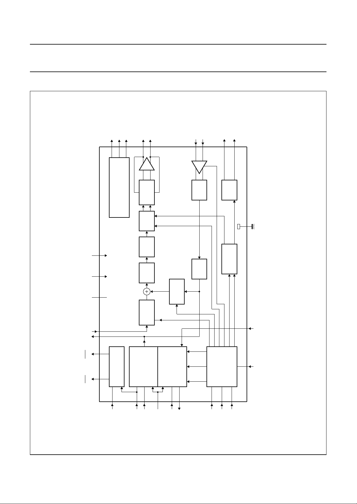
5 BLOCK DIAGRAM
REF−
REF+
V
22
20
VOLT AGE AND CURRENT
VGA
19
REFERENCE
RE+
25
RE–
23
FILTER
LOW PASS
DAC
1–BIT
V
gain tone
15
TM+
17
DAC
1–BIT
TM–
gain
33
BZ+
31
RINGER
BZ–
28814
MEA786
V
PCD5032
SS
ndbook, full pagewidth
RESET
TEST
DD
V
RPE RPIPO
TPE
PCD5032
26 30 1
9364
CLOCK AND SYNC
34
CLK
41
RAS
NOISE
SHAPER
FILTER
DIGITAL
VOLUME
CONTROL
ADPCM
DECODER
42
RAD
36
volume
DCLK
SIDETONE
level
ADPCM
DECODER
39
37
TAS
TONE
FILTER
DIGITAL
TX
mute
RX
mute
loop
44
TAD
RFM
GENERATOR
tone select
2
I C - BUS
INTERFACE
11
12
SDA
frequency/ volume
TPI
Fig.1 Block diagram (pin numbers are for QFP44 package).
A0
SCL
1997 Apr 03 4
Philips Semiconductors Product specification
ADPCM CODEC for digital cordless
PCD5032
telephones
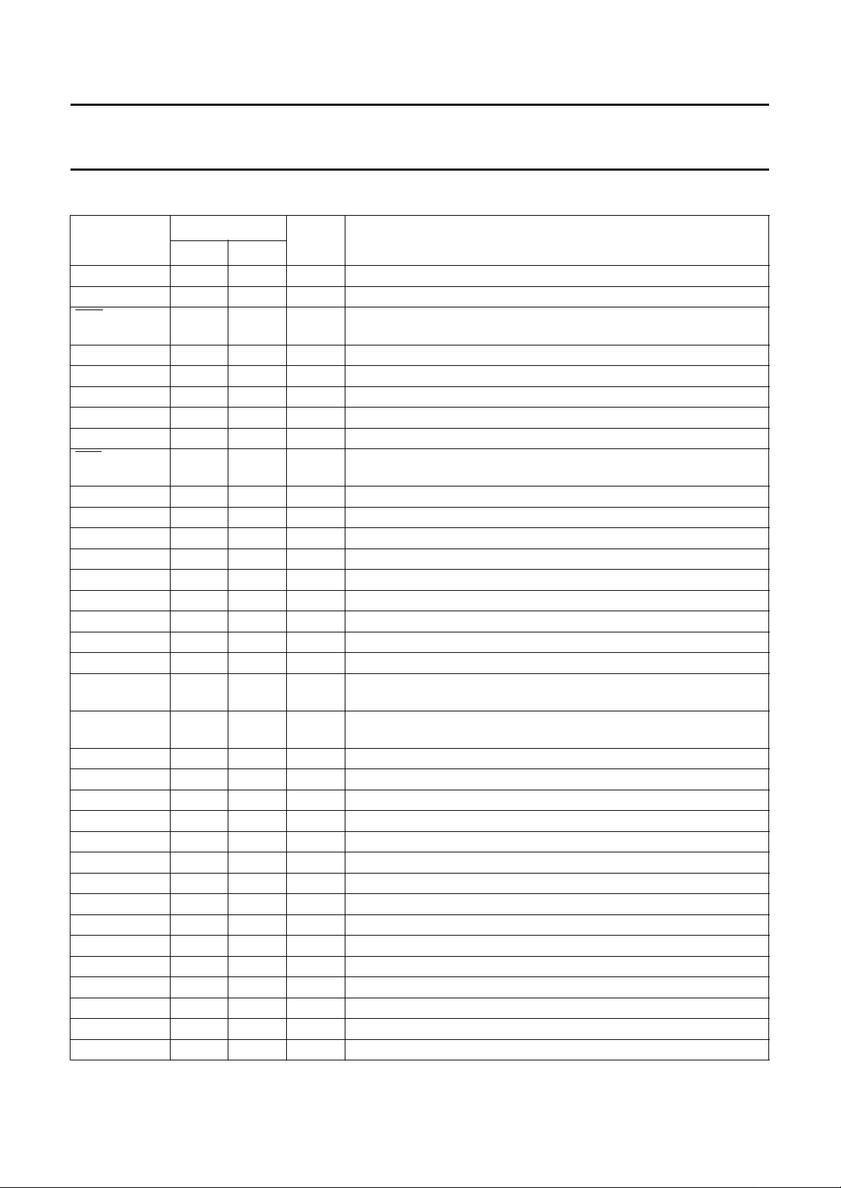
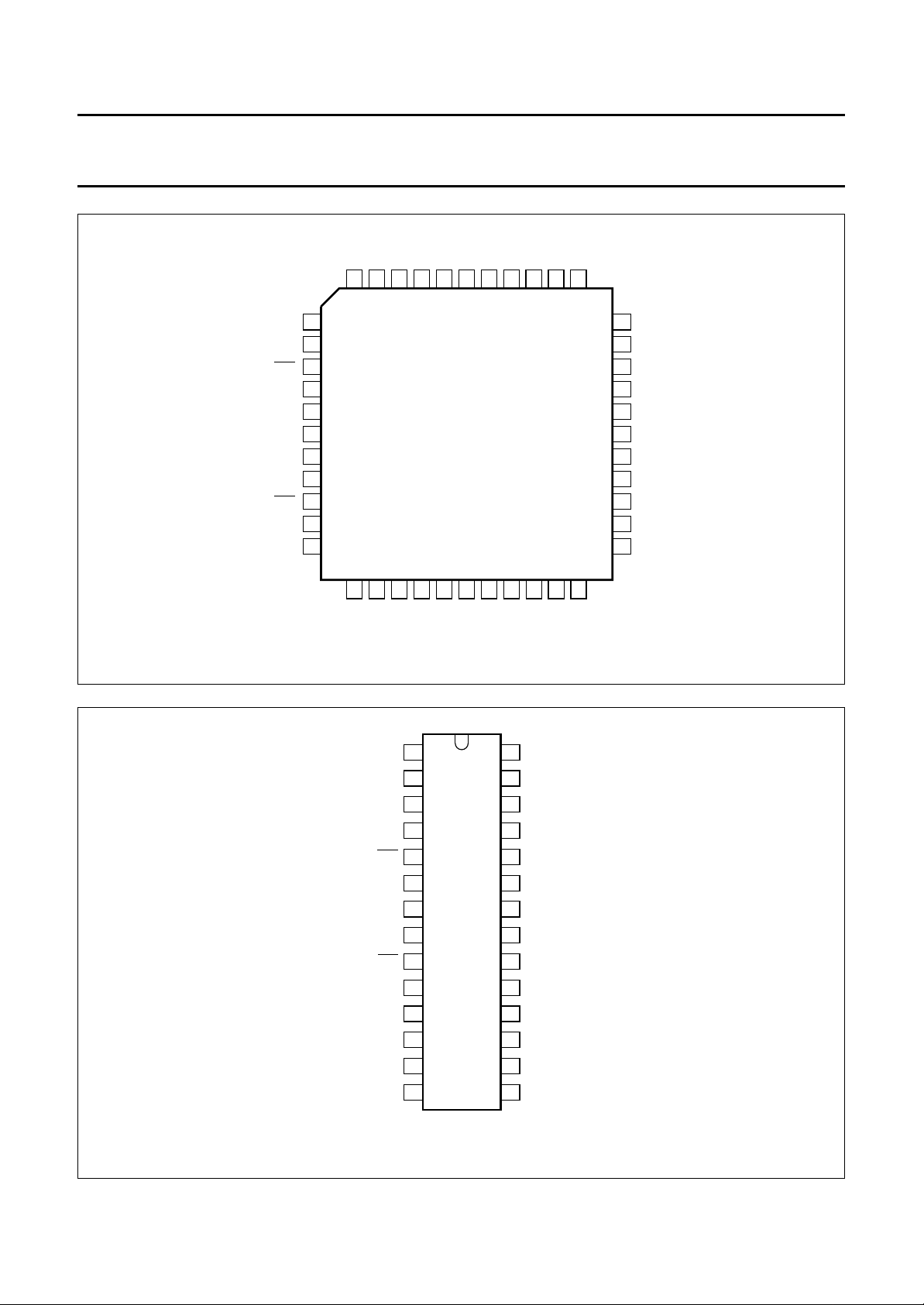
6 PINNING
(1)(2)
SYMBOL
RESET 1 4 I reset input; active HIGH
n.c. 2 −−not connected
RPE 3 5 O receiver PCM output enable (active LOW); direction from ADPCM
RPI 4 6 I receiver PCM input; direction from ADPCM interface to earpiece
n.c. 5 −−not connected
PO 6 7 O PCM data output
n.c. 7 −−not connected
TPI 8 8 I transmitter PCM input; direction from microphone to ADPCM interface
TPE 9 9 O transmitter PCM output enable (active LOW);
n.c. 10 −−not connected
SCL 11 10 I serial clock input; I
SDA 12 11 I serial data input; I
n.c. 13 −−not connected
A0 14 12 I address select input; I
TM+ 15 13 I transmitter audio positive input (microphone)
n.c. 16 −−not connected
TM− 17 14 I transmitter audio negative input (microphone)
n.c. 18 −−not connected
V
REF−
V
REF+
n.c. 21 −−not connected
VGA 22 17 O analog signal ground output
RE− 23 18 O receiver audio negative output (earpiece)
n.c. 24 −−not connected
RE+ 25 19 O receiver audio positive output (earpiece)
V
DD
n.c. 27 −−not connected
V
SS
n.c. 29 −−not connected
TEST 30 22 I test mode input; to be connected to V
BZ− 31 23 O ringer negative output
n.c. 32 −−not connected
BZ+ 33 24 O ringer positive output
CLK 34 25 I clock input
n.c. 35 −−not connected
PIN
TYPE DESCRIPTION
QFP44 SO28
interface to earpiece
direction from microphone to ADPCM interface
2
C-bus
2
C-bus
2
C-bus
19 15 O negative reference voltage output; internally generated, intended for
electret microphone supply
20 16 O positive reference voltage output; internally generated, intended for
electret microphone supply
26 20 P positive supply voltage (2.7 V to 5.5 V)
28 21 P negative supply voltage (0 V)
in normal application
SS
1997 Apr 03 5
Philips Semiconductors Product specification
ADPCM CODEC for digital cordless
PCD5032
telephones
(1)(2)
SYMBOL
PIN
QFP44 SO28
DCLK 36 26 I data clock input (ADPCM)
T AD 37 27 O transmitter ADPCM data output; direction from microphone to ADPCM
n.c. 38 −−not connected
TAS 39 28 I transmitter ADPCM sync input; direction from microphone to ADPCM
n.c. 40 −−not connected
RAS 41 1 I receiver ADPCM sync input; direction from ADPCM interface to
RAD 42 2 I receiver ADPCM data input; direction from ADPCM interface to
n.c. 43 −−not connected
RFM 44 3 I receiver fast mute input; direction from ADPCM interface to earpiece
Notes
1. QFP44 package:
Pins 1, 3, 4, 6, 8, 9, 11, 12, 14, 30, 34, 36, 37, 39, 41, 42 and 44 are digital pins.
Pins 15, 17, 23, 25, 31 and 33 are analog pins.
Pins 19, 20, 22, 26, and 28 are general pins.
2. SO28 package:
Pins 1, 2, 3, 4, 5, 6, 7, 8, 9, 10, 11, 12, 22, 25, 26, 27 and 28 are digital pins.
Pins 13, 14, 18, 19, 23 and 24 are analog pins.
Pins 15, 16, 17, 20 and 21 are general pins.
TYPE DESCRIPTION
interface
interface
earpiece
earpiece
1997 Apr 03 6
Philips Semiconductors Product specification
ADPCM CODEC for digital cordless
telephones
RFM
n.c.
44
12
SDA
43
13
n.c.
RAD
42
14
A0
TM+
handbook, full pagewidth
RESET
n.c
RPE
RPI
n.c.
PO
n.c.
TPI
TPE
n.c.
SCL
1
2
3
4
5
6
7
8
9
10
11
Fig.2 Pin configuration QFP44 (SOT205-1).
n.c.
RAS
41
40
PCD5032H
15
16
n.c.
TM–
PCD5032
n.c.
TAS
39
38
17
18
n.c.
REF–
V
n.c.
TAD
37
19
V
DCLK
36
20
REF+
35
21
n.c.
CLK
34
22
VGA
33
32
31
30
29
28
27
26
25
24
23
MEA787
BZ+
n.c.
BZ–
TEST
n.c.
V
SS
n.c.
V
DD
RE+
n.c.
RE–
handbook, halfpage
RAS
RAD
RFM
RESET
RPE
RPI
PO
TPI
TPE
SCL
SDA
A0
TM+
TM−
1
2
3
4
5
6
7
PCD5032T
8
9
10
11
12
13
MGK070
Fig.3 Pin configuration SO28 (SOT136-1).
TAS
28
TAD
27
DCLK
26
CLK
25
BZ+
24
23
BZ−
TEST
22
21
V
SS
V
20
DD
RE+
19
RE−
18
VGA
17
V
16
REF+
1514
V
REF−
1997 Apr 03 7
Philips Semiconductors Product specification
ADPCM CODEC for digital cordless
telephones
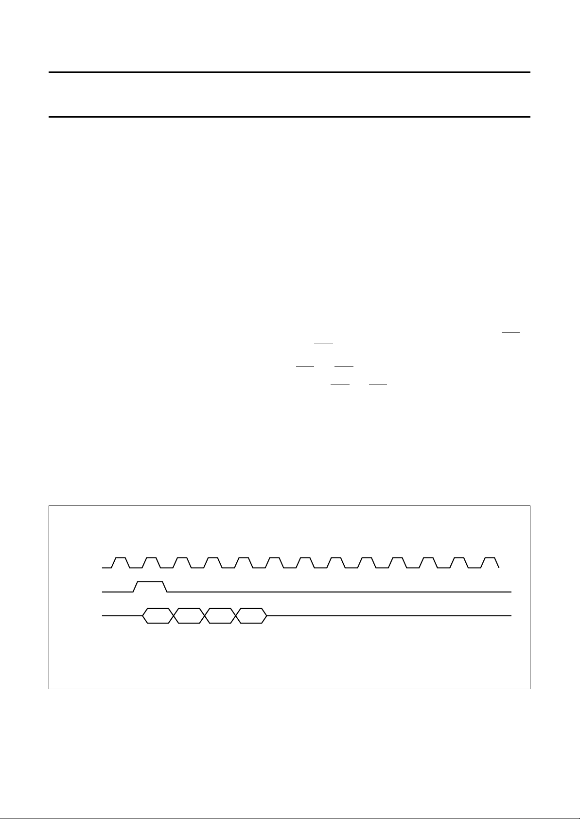
7 FUNCTIONAL DESCRIPTION
7.1 Digital interfaces
7.1.1 ADPCM
The ADPCM receive and transmit data pins, RAD and
TAD, carry 4-bit words of serial data. The received and
transmitted data are controlled separately by the
synchronization pins RAS and TAS.
On detection of a HIGH level on RAS (with a rising edge
on DCLK), the receiver will read 4 ADPCM bits on the next
4 HIGH-to-LOW transitions of DCLK. Likewise, on
reception of a HIGH level on TAS, the transmitter will
output 4 ADPCM bits on the next 4 LOW-to-HIGH
transitions of DCLK. Figure 4 is the ADPCM timing
diagram. During the time that the ADPCM data output
(TAD) is not activated, it will be in a high-impedance state,
enabling a bus structure to be used in a multi-line base
station. Input RAD has an internal pull-down resistor.
The minimum frequency on the DCLK input is1⁄54f
The maximum value equals the clock frequency, and any
value in between may be chosen. The RAS signal controls
the start of each conversion in a frame at an 8 kHz rate.
The master clock ‘CLK’ must be locked to the frequency of
‘RAS’, with a ratio f
7.1.2 PCM
To enable additional data processing in a base station
both transmit and receive linear PCM data paths are
accessible.
INTERFACE
CLK
INTERFACE
= 432 × f
RAS
.
CLK
.
PCD5032
For the receive direction the PCM data is output on pin PO
and read from pin RPI. For the transmit direction the PCM
data is output on pin PO and read from pin TPI. To enable
bus structures to be used in base stations the PCM output
PO is in high-impedance state when not active. Inputs TPI
and RPI have internal pull-down.
In a typical handset application, pin PO is directly
connected to RPI and TPI. If additional data processing is
required (echo cancellation in a base station, for example),
a data processing unit may be placed between PO and
RPI or between PO and TPI.
The data format is serial, 2’s complement, MSB first. PO
outputs 16 bits (14 data bits followed by 2 zeroes). TPI and
RPI read 14 data bits. The bit frequency is 3456 kHz
(CLK). Data output PO changes on the falling edge of CLK
(see Figs. 5 and 6).
For interfacing to digital signal processors, signals
and RPE (both active LOW) mark the position of the
transmit and receive PCM data on pin PO (see Fig.7).
TPE and RPE change on the rising edge of CLK.
Outputs RPE andTPE have low impedance only from half
a CLK cycle after the active state. The rest of the time they
are in high impedance state. Thus a wired-OR
configuration can be made when only one DSP serial input
port is used for reading both transmit and receive data.
An external pull-up is required.
TPE
handbook, full pagewidth
DCLK
RAS/TAS
RAD/TAD
01 02 03 04
MSB LSB
Fig.4 ADPCM timing.
1997 Apr 03 8
MGK073
 Loading...