

Philips PCD5013H-F1 Datasheet

DATA SH EET
Product specification
Supersedes data of 1999 Mar 15
File under Integrated Circuits, IC17
1999 Apr 12
INTEGRATED CIRCUITS
PCD5013
FLEX roaming decoder II

1999 Apr 12 2
Philips Semiconductors Product specification
FLEX roaming decoder II PCD5013
CONTENTS
1 FEATURES
2 APPLICATIONS
3 GENERAL DESCRIPTION
4 QUICK REFERENCE DATA
5 ORDERING INFORMATION
6 BLOCK DIAGRAM
7 PINNING
8 FUNCTIONAL DESCRIPTION
8.1 General
8.2 Clocking, reset and start-up
8.3 Serial Peripheral Interface (SPI)
8.4 Configuration and synchronisation
8.5 Receiver control interface
8.6 Configuration of the FLEX CAPCODE
8.7 Call data packets
8.8 Message reception
9 LIMITING VALUES
10 HANDLING
11 THERMAL CHARACTERISTICS
12 DC CHARACTERISTICS
13 AC CHARACTERISTICS
14 OSCILLATOR CHARACTERISTICS
15 TEST AND APPLICATION INFORMATION
15.1 FLEX protocol
15.2 Example applications
15.3 System block diagram
16 PACKAGE OUTLINE
17 SOLDERING
17.1 Introduction to soldering surface mount
packages
17.2 Reflow soldering
17.3 Wave soldering
17.4 Manual soldering
17.5 Suitability of surface mount IC packages for
wave and reflow soldering methods
18 DEFINITIONS
19 LIFE SUPPORT APPLICATIONS

1999 Apr 12 3
Philips Semiconductors Product specification
FLEX roaming decoder II PCD5013
1 FEATURES
• FLEX paging protocol decoder
• 16 programmable user address words
• 16 fixed temporary addresses
• 16 operator messaging addresses
• 1600, 3200 and 6400 bits/s decoding
• Any-phase or single-phase decoding
• Uses standard Serial Peripheral Interface (SPI) in slave
mode
• SSID and NID roaming support
• Backward compatible to the standard and roaming
FLEX decoder ICs
• Allows low current power-down mode operation of host
processor
• Highly programmable receiver control
• Real-time clock time base
• FLEX fragmentation and group messaging support
• Real-time clock over-the-air update support
• Compatible with synthesized receivers
• Low battery indication (external detector)
• Low cost LQFP32 plastic package
• Optional internal 4-level FSK demodulator and data
slicer
• Operates using a 76.8 or 160 kHz crystal
• Very low power consumption
• Operates at low supply voltage
• Full support for revision 1.9 of the FLEX protocol.
2 APPLICATIONS
• Numeric FLEX pagers
• Alphanumeric FLEX pagers
• Roaming FLEX pagers
• Remote metering
• Car security systems
• Personal digital assistants.
3 GENERAL DESCRIPTION
This data sheet describes the operation of the PCD5013
integrated paging decoder. It is fully compatible with other
FLEXchip ICs including the PCD5008.
The PCD5013, also referred to as the decoder, simplifies
implementation of a FLEX paging device, by being able
to interface with several off-the-shelf paging receivers and
host microcontrollers/processors. Its primary function is to
process information received and demodulated from a
FLEX radio paging channel, select messages addressed
to the paging device and communicate the message
information to the host.
The PCD5013 fully supports the FLEX protocol
(version G1.9) including all roaming aspects.
Motorola FLEXstack software, installed on the product
host processor, communicates with the PCD5013 and
interprets the codewords that are passed to the host.
The PCD5013 operates the paging receiver in an efficient
power consumption mode and enables the host to operate
in a low-power mode when monitoring a single channel for
message information.
4 QUICK REFERENCE DATA
5 ORDERING INFORMATION
SYMBOL PARAMETER CONDITIONS MIN. TYP. MAX. UNIT
V
DD
supply voltage 1.8 2.2 3.6 V
I
DD
supply current see Chapters 12 and 14 − 6.0 −µA
T
amb
operating ambient temperature −25 +25 +70 °C
f
EXTAL
external clock frequency internal demodulator not in use − 76.8 − kHz
internal demodulator in use − 160.0 − kHz
TYPE
NUMBER
PACKAGE
NAME DESCRIPTION VERSION
PCD5013H LQFP32 plastic low profile quad flat package; 32 leads; body 7 × 7 × 1.4 mm SOT358-1
1999 Apr 12 4
Philips Semiconductors Product specification
FLEX roaming decoder II PCD5013
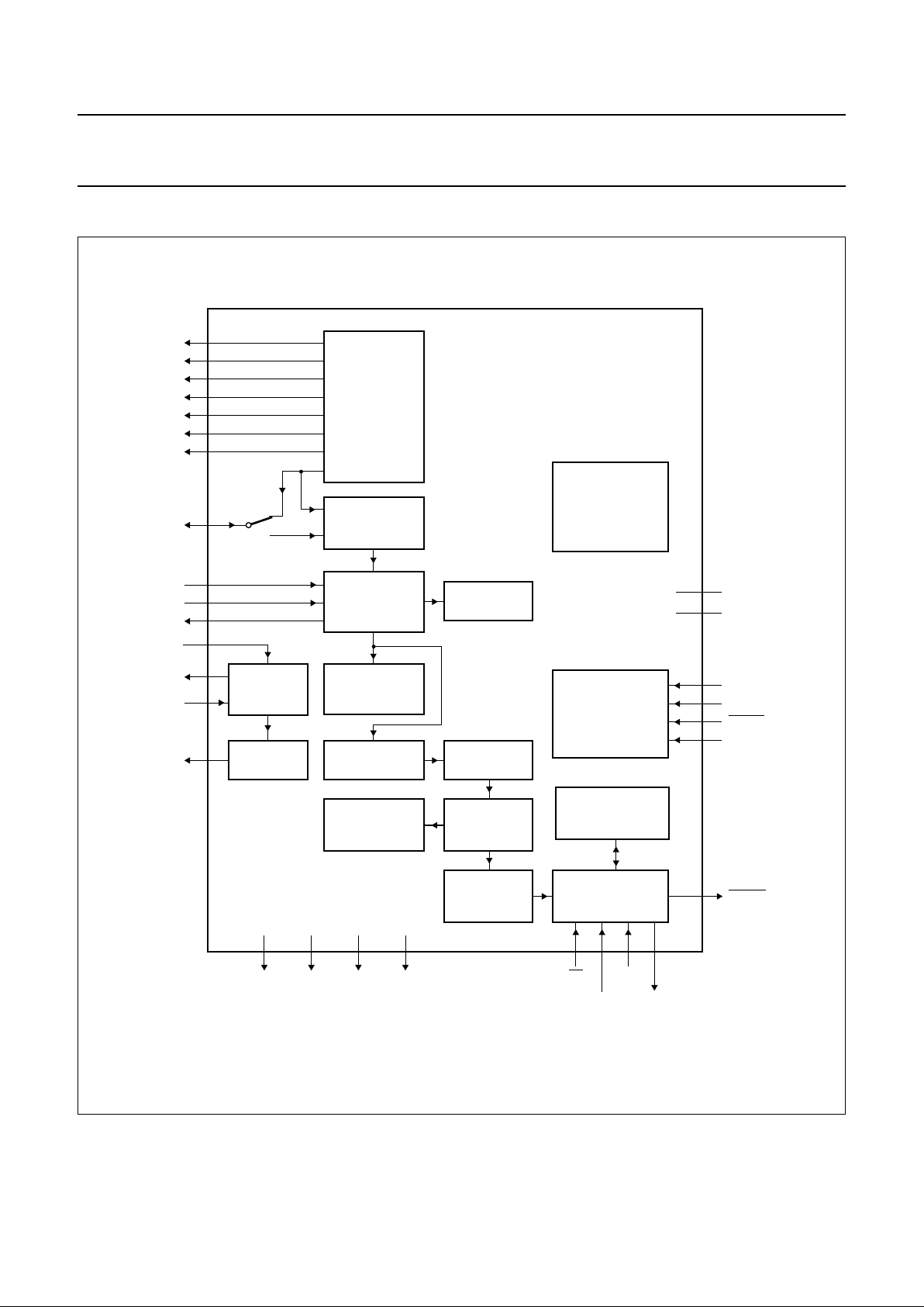
6 BLOCK DIAGRAM
Fig.1 Functional block diagram for PCD5013 pager decoder.
READY
MGR616
handbook, full pagewidth
22
S1
21
S2
20
S3
19
S4
18
S5
16
S6
15
S7
12
EXTS0
11
EXTS1
5
XTAL
2
OSCPD
6
EXTAL
32
CLKOUT
14
SYMCLK
23
S0
S0/IFIN
IFIN
27 28 30 31
26
RECEIVER
CONTROL
DEMODULATOR
&
DATA SLICER
SYNC
CORRELATOR
DE-
INTERLEAVER
76.8 kHz
OR 160 kHz
OSCILLATOR
CLOCK
GENERATOR
ADDRESS
COMPARATOR/
CORRELATOR
ERROR
CORRECTOR
NOISE
DETECTOR
SPI
BUFFER
SPI
INTERNAL
CONTROL
UNIT
EXTERNAL
CONTROL
UNIT
MISO
10
LOBAT
24
RESET
8
TEST3
4
TEST2
7, 29
V
SS1
, V
SS2
3, 13
V
DD1
, V
DD2
MOSI
SCK
SS
9
TOUT3
17
TOUT2
25
TOUT1
1
TOUT0
LOCAL
MESSAGE
FILTER
CONTROL/STATUS
REGISTERS
SYMBOL
SYNC
PCD5013

1999 Apr 12 5
Philips Semiconductors Product specification
FLEX roaming decoder II PCD5013
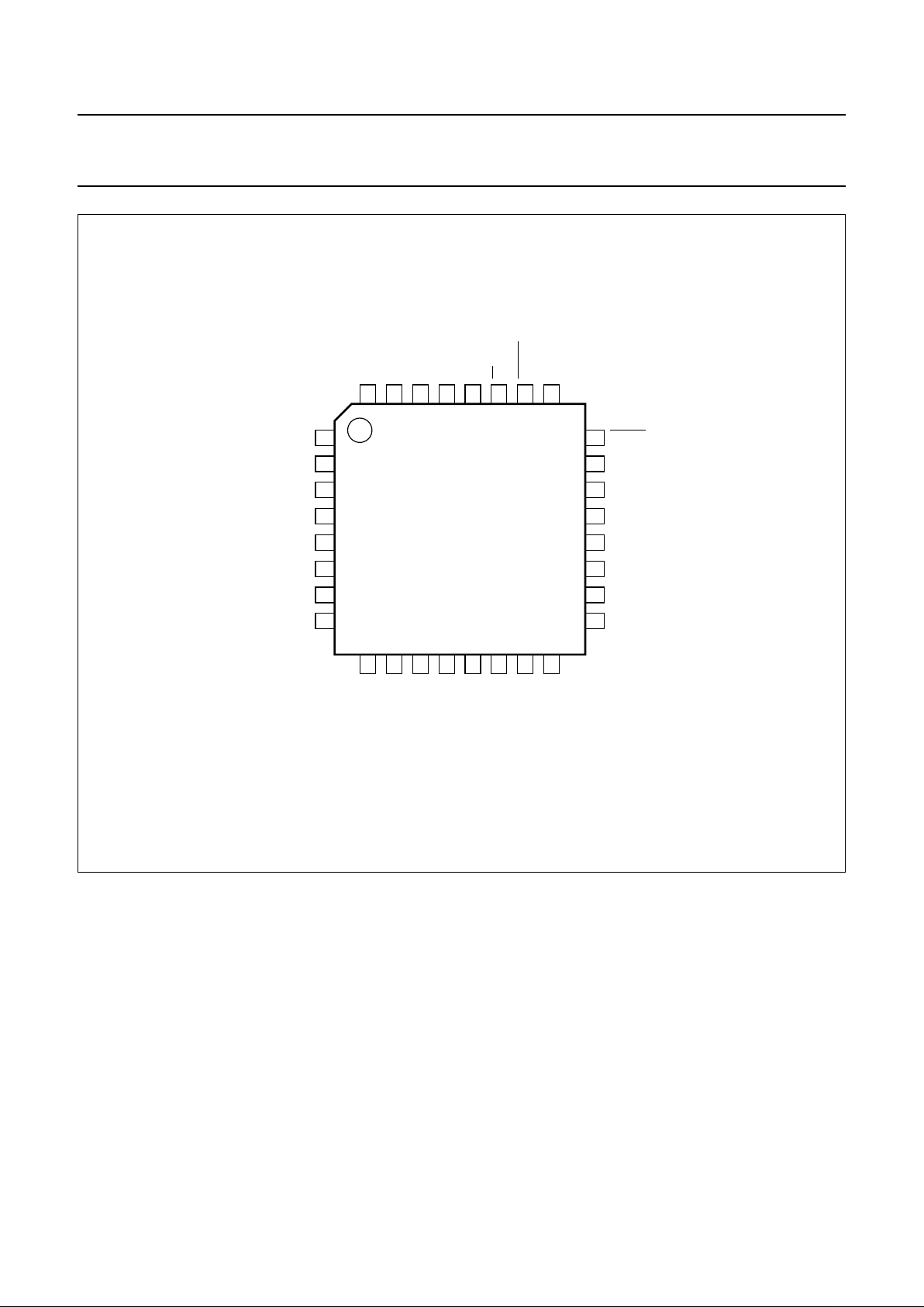
7 PINNING
Notes
1. These test outputs may be either left unconnected or connected to V
SS
in the application.
2. For a 160 kHz oscillator either a 38.4 or a 40 kHz output frequency can be selected. See Section 8.4.4.
SYMBOL PIN I/O DESCRIPTION
TOUT0 1 O 3-state test output; note 1
OSCPD 2 I internal oscillator power-down; connected to V
SS
when using the internal oscillator,
connected to VDD when using an external source
V
DD1
3 − supply voltage
TEST2 4 I manufacturing test mode input pin; has to be connected to V
SS
XTAL 5 O 76.8 or 160 kHz crystal oscillator output
EXTAL 6 I 76.8 or 160 kHz crystal oscillator input or external clock input
V
SS1
7 − ground supply
TEST3 8 I manufacturing test mode input pin; has to be connected to V
SS
TOUT3 9 O 3-state test output; note 1
LOBAT 10 I low battery voltage detect input
EXTS1 11 I most significant bit (MSB) of the symbol currently being decoded
EXTS0 12 I least significant bit (LSB) of the symbol currently being decoded
V
DD2
13 − supply voltage
SYMCLK 14 O recovered symbol clock output
S7 15 O receiver control output port, 3-state
S6 16 O receiver control output port, 3-state
TOUT2 17 O 3-state test output; note 1
S5 18 O receiver control output port, 3-state
S4 19 O receiver control output port, 3-state
S3 20 O receiver control output port, 3-state
S2 21 O receiver control output port, 3-state
S1 22 O receiver control output port, 3-state
S0/IFIN 23 I/O receiver control output port, 3-state when using external demodulator; limited
IF input 455 or 140 kHz when using internal demodulator
RESET 24 I active LOW reset input
TOUT1 25 O 3-state test output; note 1
READY 26 O output driven LOW when the PCD5013 is ready for an SPI packet
SS 27 I slave select input for SPI communications
SCK 28 I serial clock input for SPI communications
V
SS2
29 − ground supply
MOSI 30 I data input for SPI communications
MISO 31 O data output for SPI communications, 3-state
CLKOUT 32 O 38.4 kHz clock output (derived from 76.8 kHz oscillator); note 2
1999 Apr 12 6
Philips Semiconductors Product specification
FLEX roaming decoder II PCD5013
Fig.2 Pin configuration.
handbook, full pagewidth
PCD5013
MGR619
1
2
3
4
5
6
7
8
24
23
22
21
20
19
18
17
9
10
11
12
13
14
15
16
32
31
30
29
28
27
26
25
TOUT0
OSCPD
V
DD1
TEST2
XTAL
EXTAL
V
SS1
TEST3
TOUT3
LOBAT
EXTS1
EXTS0
SYMCLK
S7
S6
V
DD2
TOUT2
S5
S3
S1
S2
S0/IFIN
S4
RESET
TOUT1
SCK
V
SS2
MOSI
MISO
CLKOUT
READY
SS

1999 Apr 12 7
Philips Semiconductors Product specification
FLEX roaming decoder II PCD5013
8 FUNCTIONAL DESCRIPTION
8.1 General
The PCD5013 simplifies implementation of a FLEX
paging device by interfacing with off-the-shelf components
such as a paging receiver and a microcontroller or
microprocessor (called a host). The PCD5013 is fully
compatible with FLEXstack software which provides a
complete, platform independent, software driver for the
PCD5013.
The PCD5013 fully supports all aspects of the FLEX
protocol (version G1.9), and can operate in either
single-phase or any-phase mode. The PCD5013 supports
FLEX dynamic grouping, allowing up to 16 temporary
addresses to be enabled simultaneously. It is also capable
of retrieving real time information from a FLEX channel.
The PCD5013 connects to any receiver capable of
providing a 2-bit digital signal. The PCD5013 operates the
paging receiver in an efficient power consumption mode.
The PCD5013 has 8 receiver control lines used for
warming up, operating and shutting down a receiver in
stages.
The PCD5013 has the ability to detect a battery-low signal
from an external detector during the receiver control
sequences.
The PCD5013 carries out the following functions:
• Synchronises to a FLEX data stream
• Processes received, demodulated information
• Performs de-interleaving and error correction
• Selects calls addressed to the paging device using up to
16 programmable addresses
• Communicates the message information to the host.
The PCD5013 interfaces to a host through a serial
peripheral interface (SPI). The host can then interpret the
message information in an appropriate manner (numeric,
alphanumeric, binary, etc.). This function is provided by
the FLEXstack software.
When configured to use the internal demodulator, the
PCD5013 connects to a receiver capable of generating a
limited (i.e. 1-bit digitized) 455 or 140 kHz IF signal
(IF frequency automatically detected).
The PCD5013 enables the host to operate in a low-power
mode when monitoring a single channel for message
information. It has a 38.4 kHz clock output (40 kHz
available when using the internal demodulator) capable of
driving other devices, and has a 1-minute timer that offers
low-power support for a real-time clock function on the
host.The host can use receiver control lines which are not
required by the receiver as expansion ports to control other
peripheral devices.
8.2 Clocking, reset and start-up
8.2.1 O
SCILLATOR
The PCD5013 uses an inverting crystal oscillator.
The clock signal for the internal circuitry is derived via an
amplifier from the oscillator input pin EXTAL. Alternatively,
an external clock signal can be fed in at input pin EXTAL.
In this case the internal oscillator can be disabled by
pulling the OSCPD input pin HIGH. This reduces current
consumption and routes EXTAL directly to the internal
clock signal. When using a crystal, an external feedback
resistor and the load capacitances need to be connected
to pins EXTAL and XTAL (Fig.19). See Chapter 14 for the
recommended crystal parameters and the specification of
the oscillator transconductance to guarantee correct
start-up.
The PCD5013 oscillator can operate at either 76.8 kHz or
160 kHz by selecting the appropriate crystal. The choice of
frequency is determined by the setting of the IDE bit in the
configuration packet; see Section 8.4.4.
8.2.2 R
ESET AND START-UP CONDITIONS
The PCD5013 is reset by pulling the RESET input LOW.
After releasing the RESET by pulling it HIGH, the
PCD5013 counts 76800 clock cycles (independent of the
oscillator frequency) before pulling READY LOW to
indicate that the decoder is ready for configuration via
the SPI.
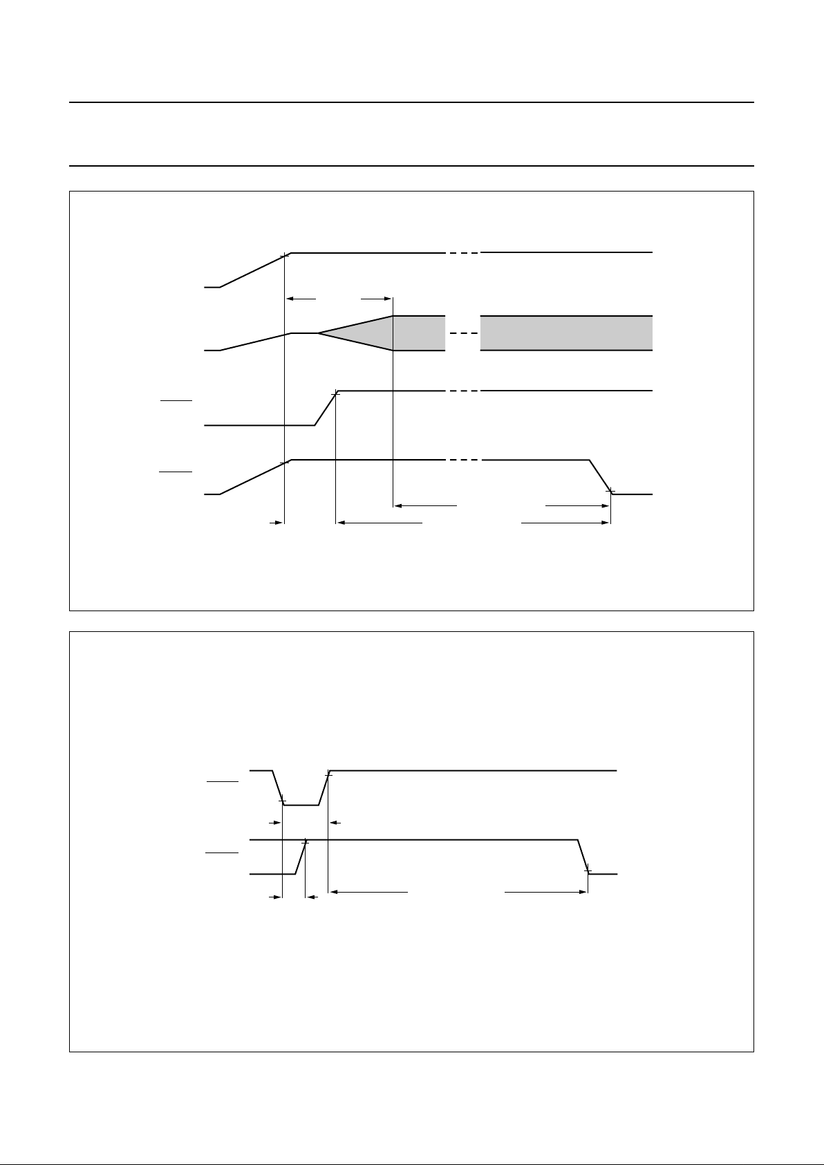
See Fig.3 and Chapter 13 for the PCD5013 timing
specifications when power is applied.
See Fig.4 and Chapter 13 for the PCD5013 timing
specifications when it is reset.
After switch-on, the PCD5013 operates in Asynchronous
mode, periodically sampling the channel for incoming
data. As soon as data is detected, the PCD5013 maintains
the receiver on to synchronize to the channel. Once the
pager is synchronized to the channel it enters
Synchronous mode, switching the receiver on only for the
programmed frames.
When the receiver is programmed for Roaming operation,
the PCD5013 sends information which allows the host to
calculate when to switch frequencies in a roaming
network.
1999 Apr 12 8
Philips Semiconductors Product specification
FLEX roaming decoder II PCD5013
Fig.3 Start-up timing.
handbook, full pagewidth
MBK031
t
h(rst)
t
WUL(osc-READY)
t
HL(RESET-READY)
t
strt(osc)
V
DD
oscillator
RESET
READY
Fig.4 Reset timing.
handbook, full pagewidth
MBK033
RESET
READY
t
LH(RESET-READY)
t
HL(RESET-READY)
t
W(rst)

1999 Apr 12 9
Philips Semiconductors Product specification
FLEX roaming decoder II PCD5013
8.3 Serial Peripheral Interface (SPI)
8.3.1 G
ENERAL
All data communication between the PCD5013 and the
host is done via the SPI using 32-bit data packets at data
rates up to 1 Mbits/s. SPI transfers are full-duplex and can
be initiated by either the host which acts as the SPI master
providing the data clock for packet transfer, or the
PCD5013 as an SPI slave.
The host can send packets to configure or control the
PCD5013 or a checksum packet to validate SPI
communication (Section 8.4.2). The PCD5013 buffers
data packets, relating to received data, into a 32 packet
transmit buffer. The PCD5013 can send either a status
packet, a part ID packet, or packets from the transmit
buffer. In the event of a buffer overflow, the PCD5013
stops decoding and clears the transmit buffer.
8.3.2 SPI
INTERCONNECT
Connection on the PCD5013 consists of a READY pin and
4 SPI pins (SS, SCK, MOSI and MISO):
READY: output signal; indicates that data is available
from the PCD5013
SS: SPI select; used as PCD5013 chip select
SCK: serial clock; output from the host used for clocking
data
MOSI: master output slave input; data output from the
host
MISO: master input slave output; data output from the
PCD5013.
8.3.3 SPI
TRANSFER INITIATED BY THE HOST
The following steps occur when the host initiates an SPI
packet transfer, see Fig.5 for event timings:
1. The host selects the PCD5013 by driving the
SS pin LOW.
2. The PCD5013 indicates that it is ready to start the
SPI transfer by driving the
READY pin LOW.
3. The host clocks each of the 32 bits of the SPI packet
by pulsing SCK. Both the host and the PCD5013
sample data on the rising edge of SCK. Packets are
sent MSB first.
4. The PCD5013 pulls the READY line HIGH, to indicate
that the transfer is complete.
5. The host waits until the READY line is pulled HIGH,
then de-selects the PCD5013 SPI by driving the
SS pin HIGH.
6. The first 5 steps are repeated for each additional
packet.
8.3.4 SPI
TRANSFER INITIATED BY THE DECODER
The following steps occur when the PCD5013 initiates an
SPI packet transfer, see Fig.6 for event timings:
1. The PCD5013 initiates the SPI transfer by driving the
READY pin LOW.
2. If the PCD5013 is not already selected, the host
selects the PCD5013 SPI by driving the SS pin LOW.
3. The host clocks each of the 32 bits of the SPI packet
by pulsing SCK. Both the host and the PCD5013
sample data on the rising edge of SCK. Packets are
sent MSB first.
4. The PCD5013 pulls the READY line HIGH, to indicate
that the transfer is complete.
5. The host may then either de-select the SPI interface of
the PCD5013 (Fig.7) by driving the SS pin HIGH or
maintain SS LOW to continue sending packets to the
PCD5013.

1999 Apr 12 10
Philips Semiconductors Product specification
FLEX roaming decoder II PCD5013
Fig.5 Typical multiple SPI transfers initiated by the host.
handbook, full pagewidth
MGK262
MISO
MOSI
SCK
Z
o(off)
(1) (5)
(4)
(2)
(3)
D31 D1 D0
D31 D1 D0
Z
o(off)
D31 D1 D0
D31 D1 D0
Z
o(off)
Z
o(off)
D31 D1 D0
D31 D1 D0
READY
SS
Numbers within parenthesis refer to sequence numbers, see Section 8.3.3.
Fig.6 Typical multiple SPI transfers initiated by the PCD5013.
handbook, full pagewidth
MGK263
MISO
MOSI
SCK
Z
o(off)
(2) (5)
(4)
(1)
(3)
D31 D1 D0
D31 D1 D0
Z
o(off)
Z
o(off)
Z
o(off)
D31 D1 D0
D31 D1 D0
D31 D1 D0
D31 D1 D0
READY
SS
Numbers within parenthesis refer to sequence numbers, see Section 8.3.4.
1999 Apr 12 11
Philips Semiconductors Product specification
FLEX roaming decoder II PCD5013
Fig.7 Multiple SPI transfers initiated by the PCD5013 with SS maintained LOW.
handbook, full pagewidth
MGK264
MISO
MOSI
SCK
Z
o(off)
D31 D1 D0
D31 D1 D0
D31 D1 D0
D31 D1 D0
D31 D1 D0
D31 D1 D0
READY
SS
1999 Apr 12 12
Philips Semiconductors Product specification
FLEX roaming decoder II PCD5013
8.3.5 SPI PACKET FORMAT
SPI data packets consist of an 8-bit ID (byte 3), followed
by 24 bits of information (byte 2 to byte 0). See Table 1,
note that bit 7 of byte 3 is the first bit on the bus.
8.3.6 SPI TIMING
See Fig.8 and Chapter 13 for the timing specifications of
the SPI.
Table 1 Packet bit assignments
BYTE BIT 7 BIT 6 BIT 5 BIT 4 BIT 3 BIT 2 BIT 1 BIT 0
3 D31 D30 D29 D28 D27 D26 D25 D24
2 D23 D22 D21 D20 D19 D18 D17 D16
1 D15 D14 D13 D12 D11 D10 D9 D8
0D7D6D5D4D3D2D1D0
Fig.8 SPI timing.
handbook, full pagewidth
MBK032
t
SCKL
t
SCKH
t
ACC(o)
Z
o(off)
t
DOV
t
h(i)(D)
t
su(i)(D)
T
cy(SCK)
t
LEAD1
SS
t
LEAD2
t
d(SS-READY)
t
READYH
t
r
t
f
t
LAG1
t
LAG2
t
SSH
READY
SCK
MISO D31 D0
D31 D0
MOSI
t
h(o)(D)
t
o(dis)

1999 Apr 12 13
Philips Semiconductors Product specification
FLEX roaming decoder II PCD5013
8.3.7 HOST-TO-DECODER PACKETS OVERVIEW
This section summarises the packets which can be sent from the host to the decoder.
Table 2 Host-to-decoder packet ID map2
PACKET
ID (HEX) TYPE SECTION
00 checksum 8.4.6
01 configuration 8.4.4
02 control 8.4.7
03 all frame mode 8.8.4
04 operator message address enable 8.6.9
05 roaming control 8.4.9
06 timing control 8.4.10
07 to 0E reserved (host should never send) −
0F receiver line control 8.5.7
10 receiver control configuration (off setting) 8.5.4
11 receiver control configuration (warm-up 1 setting) 8.5.5.3
12 receiver control configuration (warm-up 2 setting) 8.5.5.3
13 receiver control configuration (warm-up 3 setting) 8.5.5.3
14 receiver control configuration (warm-up 4 setting) 8.5.5.3
15 receiver control configuration (warm-up 5 setting) 8.5.5.3
16 receiver control configuration (3200 sps sync setting) 8.5.6.2
17 receiver control configuration (1600 sps sync setting) 8.5.6.2
18 receiver control configuration (3200 sps data setting) 8.5.6.2
19 receiver control configuration (1600 sps data setting) 8.5.6.2
1A receiver control configuration (shut-down 1 setting) 8.5.8.1
1B receiver control configuration (shut-down 2 setting) 8.5.8.1
1C to 1F special (ignored by decoder) −
20 frame assignment (frames 112 to 127) 8.6.7
21 frame assignment (frames 96 to 111) 8.6.7
22 frame assignment (frames 80 to 95) 8.6.7
23 frame assignment (frames 64 to 79) 8.6.7
24 frame assignment (frames 48 to 63) 8.6.7
25 frame assignment (frames 32 to 47) 8.6.7
26 frame assignment (frames 16 to 31) 8.6.7
27 frame assignment (frames 0 to 15) 8.6.7
28 to 77 reserved (host should never send) −
78 user address enable 8.6.6
79 to 7F reserved (host should never send) −
80 user address assignment (user address 0) 8.6.6
81 user address assignment (user address 1) 8.6.6
82 user address assignment (user address 2) 8.6.6

1999 Apr 12 14
Philips Semiconductors Product specification
FLEX roaming decoder II PCD5013
8.3.8 DECODER-TO-HOST PACKETS OVERVIEW
This section summarises the packets which can be sent from the PCD5013 to the host (Table 3).
Table 3 Decoder-to-host packet ID map
83 user address assignment (user address 3) 8.6.6
84 user address assignment (user address 4) 8.6.6
85 user address assignment (user address 5) 8.6.6
86 user address assignment (user address 6) 8.6.6
87 user address assignment (user address 7) 8.6.6
88 user address assignment (user address 8) 8.6.6
89 user address assignment (user address 9) 8.6.6
8A user address assignment (user address 10) 8.6.6
8B user address assignment (user address 11) 8.6.6
8C user address assignment (user address 12) 8.6.6
8D user address assignment (user address 13) 8.6.6
8E user address assignment (user address 14) 8.6.6
8F user address assignment (user address 15) 8.6.6
90 to FF reserved (host should never send) −
PACKET
ID (HEX) TYPE SECTION
00 block information word 8.7.9
01 address 8.7.2
02 to 57 vector or message (ID is word number in frame) 8.7.3 and 8.7.8
58 to 5F reserved −
60 roaming status 8.4.13
61 to 7D reserved −
7E receiver shutdown 8.4.12
7F status 8.4.11
80 to FE reserved −
FF part ID 8.4.5
PACKET
ID (HEX) TYPE SECTION

1999 Apr 12 15
Philips Semiconductors Product specification
FLEX roaming decoder II PCD5013
8.4 Configuration and synchronisation
8.4.1 G
ENERAL
After a reset, all configuration data has to be (re)loaded
into the PCD5013 by the host using the SPI. PCD5013
features which do not change during operation are
configured using the configuration packet (Section 8.4.4),
the receiver control packets (Section 8.5) and the address
configuration packets (Section 8.6). PCD5013 features
which can be changed during operation are configured
using the control packet. The checksum packet ensures
proper communication between the host and the
PCD5013.
8.4.2 SPI
SECURITY ALGORITHM
The PCD5013 provides a security algorithm to verify
correct SPI operation (Figs 9 and 10). The PCD5013
maintains a checksum register equal to the result of
XORing the 24 data bits of every packet it receives, except
the checksum packet 00H and special packets
1CH to 1FH. When the PCD5013 is reset, the internal
checksum register is initialized to the 24-bit part ID defined
in the part ID packet.
Immediately following a reset and whenever the host
sends a packet other than a checksum packet, the
SPI output of status and data (SPI transmit) is disabled.
The PCD5013 then initiates SPI transfers continuously,
sending the part ID packet (Section 8.4.5). Note that when
SPI transmit is disabled all decoding and timing functions
are unaffected. The SPI transmit can be enabled by
sending a checksum packet for which the checksum value
matches the checksum register.
Checksum packets sent when the SPI transmit is enabled,
are ignored by the PCD5013 irrespective of the value of
the checksum packet data bits. Thus when the PCD5013
initiates an SPI transfer and the host has no data to send,
the host should send the checksum packet so as not to
disable the SPI transmit. The data in the checksum packet
could be a null packet (32-bit stream of all zeros).
Sending a packet other than the checksum packet when
the SPI transmit is enabled causes the SPI transmit to be
disabled until a checksum packet is sent with the correct
value. Thus when the host re-configures the PCD5013
after a reset, the SPI transmit is disabled until the host
sends a checksum packet at the end of the configuration
data, with the checksum value equal to the result of
XORing together the data bits of each of the configuring
packets and the data bits of the part ID packet.
If the SPI transmit is enabled and a receiver shutdown
packet is pending, the receiver shutdown packet is sent. If
there is no receiver shutdown packet pending, but there is
a roaming status packet pending, the roaming status
packet is sent. If neither the receiver shutdown packet nor
the roaming status packet is pending and there is data in
the transmit buffer, the PCD5013 initiates an SPI transfer
sending a packet from its transmit buffer. The PCD5013
sends the status packet (which is not buffered) when the
host initiates an SPI transfer and the transmit buffer is
empty.
Fig.9 SPI transmit functional block diagram.
handbook, full pagewidth
MGR618
ROAMING STATUS REGISTER
STATUS REGISTER
SPI
SECURITY
ALGORITHM
MUX
SPI TRANSMIT REGISTER
MISO
32 × 32 DATA PACKET
FIFO TRANSMIT
BUFFER
32
RECEIVER SHUTDOWN REGISTER
32
PART ID REGISTER
32
32
32
32

1999 Apr 12 16
Philips Semiconductors Product specification
FLEX roaming decoder II PCD5013
Fig.10 SPI security algorithm.
handbook, full pagewidth
MGR617
reset
PCD5013 disables
SPI transmit
PCD5013 disables
SPI transmit
PCD5013 sets
checksum registers to
the XOR of the packet
data bits with the
checksum register bits
PCD5013 enables
SPI transmit
Y
Y
YN
N
N
PCD5013 initializes
checksum register
to part ID value
PCD5013 initiates
part ID packet
PCD5013 waits for
SPI packet from host
checksum packet?
PCD5013
SPI transmit
enabled?
packet data
matches checksum
register data?
1999 Apr 12 17
Philips Semiconductors Product specification
FLEX roaming decoder II PCD5013
8.4.3 CONFIGURATION SEQUENCE
A typical configuration and synchronisation sequence
would be as follows, see Fig.11 for event timings:
1. The PCD5013 is reset by the host.
2. After 76800 clock cycles the PCD5013 interrupts the
host to read the part ID by pulling the READY
line LOW.
3. The host pulls SS LOW at the start of each
SPI transfer and clocks out the part ID data.
4. The host configures the following aspects of PCD5013
operation:
a) General configuration (Section 8.4.4)
b) Receiver operation (Section 8.5)
c) FLEX CAPCODE configuration (Section 8.6).
The PCD5013 writes a part ID packet in response to
each incoming packet.
5. At the end of each packet the PCD5013 pulls the
READY line HIGH, and then LOW again to indicate
that packet processing is complete.
6. The host writes a control packet to enable FLEX
decoding in the PCD5013 (Section 8.4.7).
7. The host writes a checksum packet to enable SPI data
output by the PCD5013 (Section 8.4.2).
8. On recognising a SYNC word, the PCD5013
synchronises to the channel.
9. The PCD5013 initiates an SPI transfer writing the
status packet, indicating that it is now in synchronous
mode.
Fig.11 Typical configuration and synchronization sequence.
handbook, full pagewidth
MBK097
SPI
DECODER-TO-HOST
RESET
READY
SS
FLEX DATASTREAM
SPI
HOST-TO-DECODER
checksum packet
(7)
control packet
(6)
partid packet
(4)
configuration packets
(addresses, receiver etc.)
status packet
(9)
partid packet
(4)
(1)
(2)
(3)
(5) (5) (5)
(8)
SYNC
Numbers within parenthesis refer to sequence numbers, see Section 8.4.3.

1999 Apr 12 18
Philips Semiconductors Product specification
FLEX roaming decoder II PCD5013
8.4.4 CONFIGURATION PACKET (ID = 01H)
The configuration packet defines a number of different
configuration options for the PCD5013. The PCD5013
ignores this packet when decoding is enabled,
i.e. the ON bit in the control packet is set (Table 12).
DFC: disable fractional clock (Table 8). When this bit is set
and IDE is set, the CLKOUT signal generates a 40 kHz
signal (EXTAL divided-by-4). When this bit is cleared and
IDE is set, the CLKOUT signal generates a 38.4 kHz signal
(EXTAL fractionally divided by25⁄6). This bit has no effect
when IDE is cleared. Value after reset = 0.
IDE: internal demodulator enable (Table 8). When this bit
is set, the internal demodulator is enabled and the clock
frequency at EXTAL is expected to be 160 kHz. When this
bit is cleared, the internal demodulator is disabled and the
clock frequency at EXTAL is expected to be 76.8 kHz.
Value after reset = 0.
OFD: oscillator frequency difference (Tables 4 and 8).
These bits represent the maximum frequency difference
between the 76.8 kHz oscillator (accounting for ageing,
temperature variation, manufacturing tolerance etc.) and
the worst case transmitter bit rate (specified as ±25 parts
per million (ppm) in the FLEX specification).
For example, if the transmitter tolerance is ±25 ppm and
the 76.8 kHz oscillator tolerance is ±140 ppm, the
transmitter-oscillator frequency difference is ±165 ppm
and OFD should be cleared (300 ppm maximum). Value
after reset = 0. Note that configuring a smaller frequency
difference in this packet results in lower power
consumption due to higher receiver battery save ratios.
Table 4 Oscillator frequency difference
PCE: partial correlation enable (Table 8). When this bit is
set, partial correlation of addresses is enabled. When
partial correlation is enabled, the PCD5013 shuts down
the receiver before the end of the last FLEX block which
contains addresses if it can determine that none of the
addresses in that FLEX block matches any enabled
address in the PCD5013. When this bit is cleared, the
receiver is controlled as in the PCD5008. Value after
reset = 0.
OFD
1
OFD
0
FREQUENCY DIFFERENCE
(ppm)
00±300
01±150
10±75
11±0
SP: signal polarity (Tables 8, 5 and 6). These bits set the
polarity of EXTS1 and EXTS0 input signals. The polarity of
the EXTS1 and EXTS0 bits is determined by the receiver
design. Value after reset = 0.
Table 5 Input signal polarity
Table 6 FLEX 4 level FSK modulation (SP = 00)
SME: synchronous mode enable (Table 8). When this bit
is set, a status packet is sent automatically whenever the
synchronous mode update (SMU) bit in the status packet
is set. This happens whenever a change occurs in the
synchronous mode (SM) status bit, which indicates that
the decoder is synchronized to a FLEX data stream.
The host can use the SM bit in the status packet as an
in-range/out-of-range indication. Value after reset = 0.
COD: clock output disable (Table 8). When this bit is
cleared, a 38.4 or 40 kHz signal is output on the
CLKOUT pin (depending on the values of IDE and DFC).
When this bit is set, the CLKOUT pin is driven LOW. Value
after reset = 0.
• Setting and clearing this bit can cause pulses on the
CLKOUT pin that are less than one half the 38.4 kHz
period.
• When the clock output is enabled and not set for
intermittent operation (see ICO in this packet), the
CLKOUT pin always outputs the clock signal even when
the PCD5013 is in reset (as long as a clock signal is
available to the PCD5013 oscillator).
• When the PCD5013 is used in internal demodulator
mode (i.e. uses a 160 kHz oscillator), the CLKOUT pin
is 80 kHz from reset until the time the IDE bit is set.
SP
1
SP
0
SIGNAL POLARITY
EXTS1 EXTS0
0 0 normal normal
0 1 normal inverted
1 0 inverted normal
1 1 inverted inverted
EXTS1 EXTS0
DEVIATION
(Hz)
1 0 +4800
1 1 +1600
01 −1600
00 −4800

1999 Apr 12 19
Philips Semiconductors Product specification
FLEX roaming decoder II PCD5013
LBP: low battery polarity (Table 8). This bit defines the
polarity of the PCD5013’s LOBAT pin: When this bit is set,
a HIGH at input LOBAT represents a low battery condition.
The LB bit in the status packet is initialized to the inverse
(i.e. inactive) value of the LBP bit when the PCD5013 is
turned on (by setting the ON bit in the control packet).
When the PCD5013 is turned on, the first low battery
update in the status packet is sent to the host when a low
battery condition is detected on the LOBAT pin. Value
after reset = 0.
MOT: maximum off time (Table 8). When this bit is set, the
PCD5013 assumes that the service provider leaves up to
1 minute between transmitted frames. When this bit is
clear, the PCD5013 assumes that there can be up to
4 minutes between transmitted frames. This bit has no
effect if AST in the Timing Control Packet is non-zero.
Value after reset = 0.
MTE: minute timer enable (Table 8). When this bit is set,
a status packet is sent at one minute intervals with the
minute time-out (MT) bit in the status packet set. When
this bit is clear, the internal 1-minute timer stops counting.
See Section 8.4.8 for details of 1-minute timer operation.
Note that the minute timer is not accurate using a 160 kHz
oscillator until the IDE bit is set. Value after reset = 0.
ICO: intermittent clock out (Table 8). When this bit is clear
and COD is clear, a 38.4 or 40 kHz (depending on the
values of IDE and DFC) signal is output on the CLKOUT
pin. When this bit is set and COD is clear, the clock is only
output on the CLKOUT pin while the receiver is not in the
Off state. The clock is output for a few cycles before the
receiver transitions from the off state and for a few cycles
after the receiver transitions to the off state (this is to insure
that the receiver receives enough clocks to detect and
process the changes to and from the off state).
The CLKOUT pin is driven LOW when it is not driving a
clock.
Note that when the clock is automatically enabled and
disabled (i.e. when ICO is set), the CLKOUT signal
transitions are clean (i.e. no pulses less than half the clock
period) when it transitions between no clock and clocked
output. This bit has no effect when COD is set. Value after
reset = 0.
8.4.5 P
ART ID P ACKET (ID = FFH)
The part ID packet is output by the PCD5013 SPI
whenever the SPI transmit is disabled due to the
checksum feature. The value of the part ID packet for the
PCD5013 is FF000308H.
MDL: model (Table 9). The PCD5013 model value is 0.
CID: compatibility ID (Table 9). This value describes other
parts with the same model number, which are compatible
with this part.
Table 7 CID Compatibilities
REV: revision (Table 9). This identifies the manufacturing
version of the PCD5013. For the PCD5013 the value is 8.
8.4.6 C
HECKSUM PACKET (ID = 00H)
See Table 10 for checksum packet bit assignment.
CV: checksum value (24 bits), see Section 8.4.2.
BIT COMPATIBILITY
VALUE FOR
PCD5013
CID
0
Alphanumeric Decoder I 1 (true)
CID
1
Roaming Decoder I 1 (true)
CID
2
Numeric Decoder 0 (false)
Table 8 Configuration packet bit assignments
BYTE BIT 7 BIT 6 BIT 5 BIT 4 BIT 3 BIT 2 BIT 1 BIT 0
300000001
2 0 DFC 0 0 0 IDE OFD
1
OFD
0
100000PCESP
1SP0
0 SME MOT COD MTE LBP ICO 0 0

1999 Apr 12 20
Philips Semiconductors Product specification
FLEX roaming decoder II PCD5013
Table 9 Part ID packet bit assignments
Table 10 Checksum packet bit assignments
BYTE BIT 7 BIT 6 BIT 5 BIT 4 BIT 3 BIT 2 BIT 1 BIT 0
311111111
2 MDL
1
MDL
0
CID
13
CID
12
CID
11
CID
10
CID
9
CID
8
1 CID
7
CID
6
CID
5
CID
4
CID
3
CID
2
CID
1
CID
0
0 REV
7
REV
6
REV
5
REV
4
REV
3
REV
2
REV
1
REV
0
BYTE BIT 7 BIT 6 BIT 5 BIT 4 BIT 3 BIT 2 BIT 1 BIT 0
300000000
2CV23CV
22
CV
21
CV
20
CV
19
CV
18
CV
17
CV
16
1CV15CV
14
CV
13
CV
12
CV
11
CV
10
CV
9
CV
8
0CV
7CV6
CV
5
CV
4
CV
3
CV
2
CV
1
CV
0

1999 Apr 12 21
Philips Semiconductors Product specification
FLEX roaming decoder II PCD5013
8.4.7 CONTROL PACKET (ID = 02H)
The control packet defines a number of different control
bits for the PCD5013.
FF: force frame 0 to 7 (Table 12). When set, each of these
bits forces the PCD5013 to decode one of the FLEX
frames 0 to 7 irrespective of the system collapse value (for
details of collapse values see Section 8.6.2). For example,
if the system collapse causes the PCD5013 to decode
frames 0, 32, 64 and 96, setting FF2 causes the PCD5013
to also decode FLEX frame 2. This may be used to
acquire transmitted time information or channel attributes
(e.g. Local ID). Value after reset = 0.
SPM: single phase mode (Table 12). When this bit is set,
the PCD5013 decodes only one of the transmitted phases.
When this bit is clear, the PCD5013 decodes all
transmitted phases. This value is determined by the
CAPCODE (Section 8.6). A change to this bit while the
PCD5013 is on does not take effect until the next block 0
of a frame. Value after reset = 0.
PS: phase select (Tables 11 and 12). When the SPM bit is
set, these bits define which phase the PCD5013 shall
decode. This value is determined by the CAPCODE
(Section 8.6). A change to these bits, while the PCD5013
is on, does not take effect until the next block 0 of a frame.
Value after reset = 0.
Table 11 Phase selection (by PS bits)
PS
1
PS
0
DECODED PHASE (BASED ON
FLEX DATA RATE)
1600 bits/s 3200 bits/s 6400 bits/s
00AAA
01AAB
10 A C C
11 A C D
SBI: send block information words (BIW) 2 to 4
(Table 12). When this bit is set, BIWs with time and date
information and BIWs received in error are sent to the host,
(Section 8.7.9). Value after reset = 0.
MTC: minute timer clear (Table 12). Setting this bit causes
the 1-minute timer to restart from 0 (Section 8.4.8).
ON: turn on decoder (Table 12). When this bit is set, the
PCD5013 decodes FLEX signals. If this bit is cleared,
signal processing stops. However, to assure proper
operation, the PCD5013 requires that it be set into
asynchronous mode when turned off. To achieve that the
following sequence must be used:
1. Send control packet with ON bit clear (decoder off)
2. Send control packet with ON bit set (decoder on)
3. Send control packet with ON bit clear (decoder off).
Timing between these steps is specified below and is
measured from the positive edge of the last clock of one
packet to the positive edge of the last clock of the next
packet.
• The minimum time between steps 1 and 2 is the greater
of 2 ms or the programmed shut-down time.
The programmed shut-down time is the sum of all of the
times programmed in the used receiver shut-down
settings packets.
• There is no maximum time between steps 1 and 2.
• The minimum time between steps 2 and 3 is 2 ms.
• The maximum time between steps 2 and 3 is the
programmed warm-up time minus 2 ms.
The programmed warm-up time is the sum of all the
times programmed in the used receiver warm-up
settings packets.
EAE: end of addresses enable. When this bit is set, the EA
bit in the Status Packet is PCD5013 set immediately after
the PCD5013 decodes the last address word in the frame
if any of the enabled PCD5013 addresses was detected in
the frame. When this bit is cleared, the EA bit is never set.
Table 12 Control packet bit assignments
BYTE BIT 7 BIT 6 BIT 5 BIT 4 BIT 3 BIT 2 BIT 1 BIT 0
300000010
2FF
7FF6
FF
5
FF
4
FF
3
FF
2
FF
1
FF
0
1 0 SPM PS
1
PS
0
0000
0 0 SBI 0 MTC 0 0 EAE ON

1999 Apr 12 22
Philips Semiconductors Product specification
FLEX roaming decoder II PCD5013
8.4.8 OPERATING THE 1-MINUTE TIMER
The PCD5013 provides a 1-minute timer which allows the
host to implement a time-of-day function while maintaining
low-power operation. The 1-minute timer is enabled using
the MTE bit in the configuration packet (Section 8.4.4).
When the 1-minute timer is enabled, a status packet is
sent at 1-minute intervals with the MT bit set
(Section 8.4.11). When the MTE bit is clear, the internal
1-minute timer stops counting. When the host sends a
control packet with MTC bit set, the 1-minute timer restarts
from 0. This allows accurate setting of a time-of-day
function.
8.4.9 R
OAMING CONTROL PACKET (ID = 05H)
The roaming control packet controls the features of the
PCD5013 that allow implementation of a roaming pager.
IRS: ignore re-synchronization signal (Table 13). When
this bit is set, the PCD5013 does not go asynchronous
when detecting an Ar or Ar signal during searches for
A-words. It merely reports that the re-synchronization
signal was received by setting RSR to 1 in the Roaming
Status packet. This allows the host to decide what to do
when the paging device is synchronous to more than one
channel and only one channel is sending the
re-synchronization signal. It also prevents the PCD5013
from losing synchronization when it detects the
re-synchronization signal while the paging device is
checking an unknown channel. This bit is set and cleared
by the host. Value after reset = 0.
NBC: network bit check (Table 13). Setting this bit enables
reporting of the received network bit value (NBU and n) in
the Roaming Status Packet. Setting this bit also makes the
PCD5013 abandon a frame after the Frame Info word
without synchronizing to the frame if the frame information
word is uncorrectable or if the n bit in the frame information
word is not set. If the PCD5013 is in synchronous mode
when this occurs (probably due to synchronizing to a
second channel), it maintains synchronization to the
original channel.
If the PCD5013 is in asynchronous mode when this
occurs, it stays in asynchronous mode and end the A-word
search. This is done to avoid synchronizing to a
non-roaming channel when searching for roaming
channels. This bit is set and cleared by the host. Value
after reset = 0.
MCM: manual collapse mode (Table 13). When this bit is
set, the PCD5013 behaves as if the system collapse
was 7. The PCD5013 does not apply the received system
collapse to the AF bits. When this bit is set, the received
system collapse is reported to the host via SCU and RSC
in the Roaming Status Packet. This is so the host can
modify the AF bits based on the system collapse of the
channel. This bit is set and cleared by the host. Value after
reset = 0.
IS1: invert EXTS1 (Table 13). Setting this bit inverts the
expected polarity of the EXTS1 pin from the way it is
configured by SP 1 in the Configuration Packet (e.g. if both
IS1 and SP 1 are set, the polarity of the EXTS1 pin is
untouched). This bit is intended to be changed when a
change in a channel changes the polarity of the received
signal. This bit is set and cleared by the host. This bit has
the equivalent effect when using the internal demodulator.
Value after reset = 0.
SDF: stop decoding frame (Table 13). Setting this bit
causes the PCD5013 to stop decoding a frame without
losing frame synchronization. This bit is set by the host,
and cleared by the PCD5013 once it has been processed.
The packet with the SDF bit set must be sent after
receiving the status packet with EA bit set. It must be sent
within 40 ms of the end of block in which the PCD5013 set
the EA bit. Value after reset = 0.
RSP: receiver shutdown packet enable (Table 13). When
this bit is set, a Receiver Shutdown Packet is sent
whenever the receiver is shut down. The receiver
shutdown packet informs the host that the receiver
shutdown, and gives the time period before the PCD5013
automatically warms the receiver back up. Value after
reset = 0.
Table 13 Roaming Control Packet bit assignments
BYTE BIT 7 BIT 6 BIT 5 BIT 4 BIT 3 BIT 2 BIT 1 BIT 0
300000101
2 IRS NBC MCM IS1 SDF RSP SND CND
1 RND ABI SAS DAS AF
11
AF
10
AF
9
AF
8
000MFC
1
MFC
0
0 0 MCO
1
MCO
0

1999 Apr 12 23
Philips Semiconductors Product specification
FLEX roaming decoder II PCD5013
SND: start noise detect (Table 13). Setting this bit while
the PCD5013 is battery saving causes it to warm-up the
receiver, run a noise detect, and report the result of the
noise detect via NDR in the Roaming Status Packet.
This bit is set by the host, and cleared by the PCD5013
once it has been processed. If the time comes for the
PCD5013 to warm-up automatically or the SAS bit is set
while an SND is being processed, the noise detect is
abandoned and the abandoned noise detect result
(NDR = 01) is sent in the Roaming Status Packet. Value
after reset = 0.
CND: continuous noise detect (Table 13). Setting this bit
causes the PCD5013 to do continuous noise detects
during the decoded block data of a frame. The results of
the noise detect is only reported if noise is detected
(NDR = 11). Only one noise detected result (NDR = 11) is
sent per block. If the PCD5013 has not completed a noise
detect when it shuts down for the frame, that noise detect
is abandoned, but no abandon result (NDR = 01) is sent.
This bit is set and cleared by the host. Value after
reset = 0.
RND: report noise detects (Table 13). Setting this bit
causes the PCD5013 to report the results of the noise
detects it does under normal asynchronous operation
(when first turned on and when asynchronous).
The results of the noise detect is reported via NDR in the
Roaming Status Packet. This bit is set and cleared by the
host. Value after reset = 0.
ABI: all block information words (Table 13). When this bit
is set, the PCD5013 sends all received Block Information
words 2-4 to the host. Note: Setting the SBI bit in the
Control Packet only enables errored and real-time clock
related block info words. Value after reset = 0.
SAS: start A-word search (Table 13). Setting this bit while
in asynchronous battery save mode causes the PCD5013
to warm-up the receiver and run an A-word search.
If, during the A-word search, the PCD5013 finds sufficient
FLEX signal, it enters synchronous mode and start
decoding the frame. If the A-word search times-out without
finding sufficient FLEX signal, it enters a battery save
mode and continue doing periodic noise detects.
The time-out for the A-word searches is controlled by the
AST bits in the Timing Control Packet and the MOT bit in
the Configuration Packet. The A-word search takes priority
over noise detects. Therefore, if the PCD5013 is
performing an A-word search and the time comes to do
automatic noise detect, the noise detect is not performed.
This bit is set by the host, and cleared by the PCD5013
once it has been acted on. Value after reset = 0.
MFC: missed frame control (Tables 14 and 13). These bits
control the frames for which missing frame data (MS1,
MFI, MS2, MBI, and MAW) is reported in the Roaming
Status Packet. Value after reset = 0.
Table 14 Missed Frame Control (MFC bits)
MCO: maximum carry on (Table 13). The value of these
bits sets the maximum carry on that the PCD5013 follows.
For example, if the PCD5013 receives a carry on of 3 over
the air and MCO is set to 1, the PCD5013 only carries on
for one frame. Value after reset = 3.
DAS: disable A-word search (Table 13). When this bit is
set, an A-word search does not automatically occur after a
noise detect in asynchronous mode finds FLEX signal.
This includes automatic noise detects and noise detects
initiated by the host by setting SND. The PCD5013 shuts
down the receiver after the noise detect completes
regardless of the result. When this bit is cleared, A-word
searches occur after a noise detect finds signal in
asynchronous mode. Value after reset = 0.
MFC
1
MFC0MISSING FRAME DATA REPORTED
0 0 never
0 1 only during frames 0 through 3
1 0 only during frames 0 through 7
1 1 always
 Loading...