

Philips pcd5002a DATASHEETS

INTEGRATED CIRCUITS
DATA SH EET
PCD5002A
Enhanced Pager Decoder for
APOC1/POCSAG
Product specification
File under Integrated Circuits, IC17
1999 Jan 08

Philips Semiconductors Product specification
Enhanced Pager Decoder for
APOC1/POCSAG
CONTENTS
1 FEATURES
2 APPLICATIONS
3 GENERAL DESCRIPTION
4 ORDERING INFORMATION
5 LICENSE
6 BLOCK DIAGRAM
7 PINNING
8 FUNCTIONAL DESCRIPTION
8.1 Introduction
8.2 The POCSAG paging code
8.3 The APOC1 paging code
8.4 Error correction
8.5 Operating states
8.6 ON status
8.7 OFF status
8.8 Reset
8.9 Bit rates
8.10 Oscillator
8.11 Input data processing
8.12 Battery saving
8.13 POCSAG synchronization strategy
8.14 APOC1 synchronization strategy
8.15 Call termination
8.16 Enhanced call termination
8.17 Call data output format
8.18 Error type indication
8.19 Data transfer
8.20 Continuous data decoding
8.21 Receiver and oscillator control
8.22 Demodulator quick charge
8.23 External receiver control and monitoring
8.24 Battery condition input
8.25 Synthesizer control
8.26 Serial microcontroller interface
8.27 Decoder I2C-bus access
8.28 External interrupt
8.29 Interrupt masking
8.30 Status/control register
8.31 Pending interrupts
8.32 Out-of-range indication
8.33 Real-time clock
8.34 Periodic interrupt
8.35 Received call delay
8.36 Alert generation
8.37 Alert cadence register (03H; write)
8.38 Acoustic alert
8.39 Vibrator alert
8.40 LED alert
PCD5002A
8.41 Warbled alert
8.42 Direct alert control
8.43 Alert priority
8.44 Cancelling alerts
8.45 Automatic POCSAG alerts
8.46 SRAM access
8.47 RAM write address pointer (06H; read)
8.48 RAM read address pointer (08H; read/write)
8.49 RAM data output register (09H; read)
8.50 EEPROM access
8.51 EEPROM address pointer (07H; read/write)
8.52 EEPROM data I/O register (0AH; read/write)
8.53 EEPROM access limitations
8.54 EEPROM read operation
8.55 EEPROM write operation
8.56 Invalid write address
8.57 Incomplete programming sequence
8.58 Unused EEPROM locations
8.59 Special programmed function allocation
8.60 Synthesizer programming data
8.61 Identifier storage allocation
8.62 Voltage doubler
8.63 Level-shifted interface
8.64 Signal test mode
9 OPERATING INSTRUCTIONS
9.1 Reset conditions
9.2 Power-on reset circuit
9.3 Reset timing
9.4 Initial programming
10 LIMITING VALUES
11 DC CHARACTERISTICS
12 DC CHARACTERISTICS (WITH VOLTAGE
CONVERTER)
13 OSCILLATOR CHARACTERISTICS
14 AC CHARACTERISTICS
15 APPLICATION INFORMATION
16 PACKAGE OUTLINE
17 SOLDERING
17.1 Introduction to soldering surface mount
packages
17.2 Reflow soldering
17.3 Wave soldering
17.4 Manual soldering
17.5 Suitability of surface mount IC packages for
wave and reflow soldering methods
18 DEFINITIONS
19 LIFE SUPPORT APPLICATIONS
20 PURCHASE OF PHILIPS I2C COMPONENTS
1999 Jan 08 2

Philips Semiconductors Product specification
Enhanced Pager Decoder for
APOC1/POCSAG
1 FEATURES
• Wide operating supply voltage range: 1.5 to 6.0 V
• EEPROM programming requires only 2.0 V supply
• Low operating current: 50 µA typ. (ON), 25 µA typ.
(OFF)
• Temperature range −25 to +70 °C
•
“CCIR radio paging Code No. 1”
• Supports Advanced Pager Operator’s Code Phase 1
(APOC1) for extended battery economy
• 512, 1200 and 2400 bits/s data rates using 76.8 kHz
crystal
• Built-in data filter (16 times oversampling) and bit clock
recovery
• Advanced ACCESS
• 2-bit random and (optional) 4-bit burst error correction
• Up to 6 user addresses Receiver Identity Codes (RICs),
each with 4 functions/alert cadences
• Optional automatic call termination when bit error rate is
high
• Up to 6 user address frames, independently
programmable
• Standard POCSAG sync word, plus up to 4 user
programmable sync words
• Continuous data decoding upon reception of user
programmable sync word (optional)
• Received data inversion (optional)
• Call alert via beeper, vibrator or LED
• 2-level acoustic alert using single external transistor
• Alert control: automatic (POCSAG type), via cadence
register or alert input pin
• Separate power control of receiver and RF oscillator for
battery economy
• Dedicated pin for easy control of superheterodyne
receiver
• Synthesizer set-up and control interface (3-line serial)
• On-chip EEPROM for storage of user addresses (RICs),
pager configuration and synthesizer data
• On-chip SRAM buffer for message data
synchronization algorithm
(POCSAG) compatible
PCD5002A
2
• Slave I
message data, status/control and EEPROM
programming (data transfer at up to 100 kbits/s)
• Wake-up interrupt for microcontroller, programmable
polarity
• Direct and I2C-bus control of operating status (ON/OFF)
• Battery-low indication (external detector)
• Out-of-range condition indication
• Real-time clock reference output
• On-chip voltage doubler
• Interfaces directly to UAA2080 and UAA2082 paging
receivers.
2 APPLICATIONS
• Advanced display pagers (POCSAG and APOC1)
• Basic alert-only pagers
• Information services
• Personal organizers
• Telepoint
• Telemetry/data transmission.
3 GENERAL DESCRIPTION
The PCD5002A is a very low power pager decoder and
controller, capable of handling both standard POCSAG
and the advanced APOC1 code. Continuous data
decoding upon reception of a dedicated sync word is
available for news pager applications.
Data rates supported are 512, 1200 and 2400 bits/s using
a single 76.8 kHz crystal. On-chip EEPROM is
programmable using a minimum supply voltage of 2.0 V,
allowing ‘over-the-air’ programming. I
C-bus interface to microcontroller for transfer of
2
C-bus compatible.
4 ORDERING INFORMATION
TYPE NUMBER
NAME DESCRIPTION VERSION
PCD5002AH LQFP32 plastic low profile quad flat package; 32 leads; body 7 × 7 × 1.4 mm SOT358-1
1999 Jan 08 3
PACKAGE
Philips Semiconductors Product specification
Enhanced Pager Decoder for
PCD5002A
APOC1/POCSAG
5 LICENSE
Supply of this IC does neither convey nor express an implied license under any patent right to use this in any APOC
application.
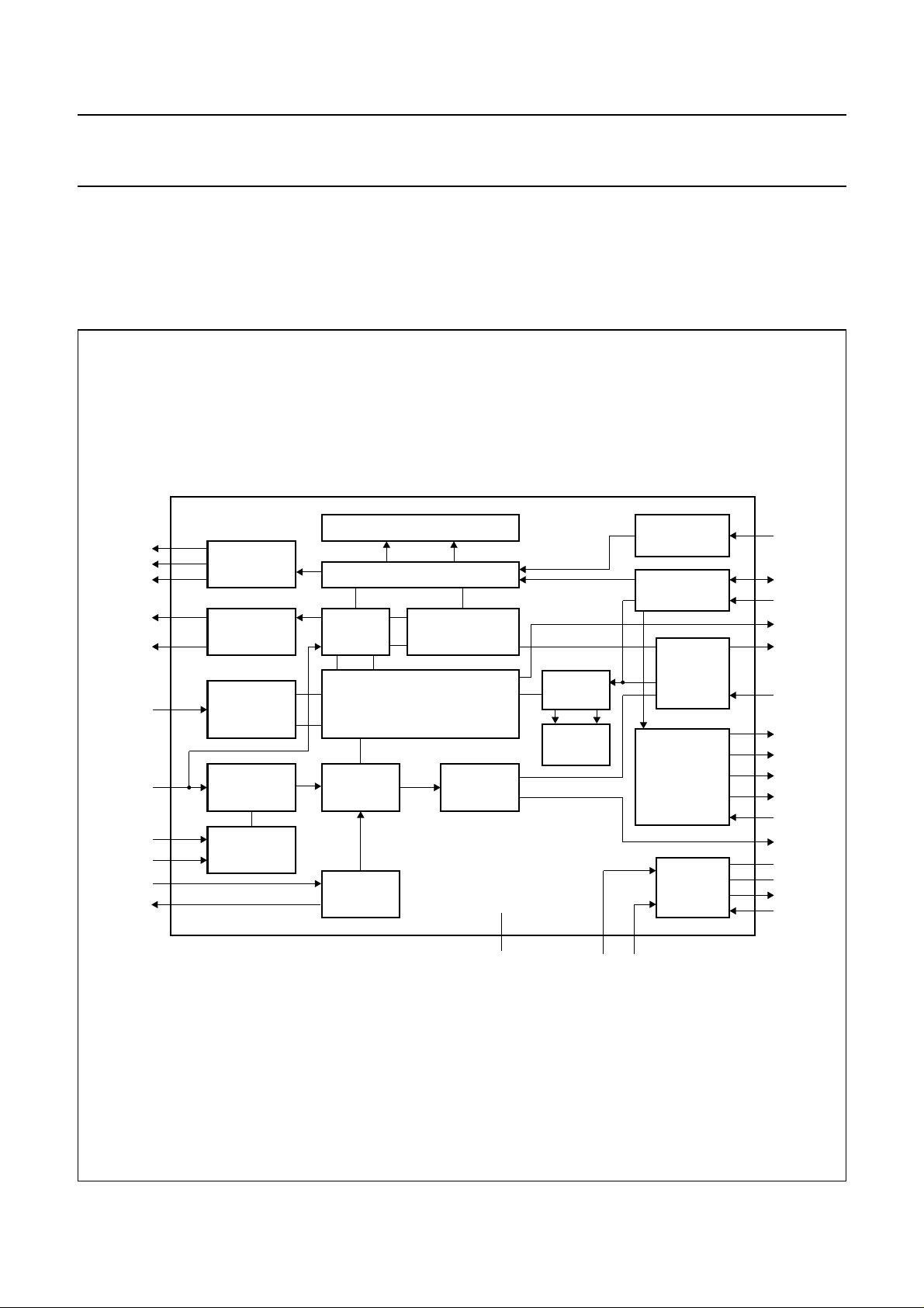
6 BLOCK DIAGRAM
handbook, full pagewidth
10
22
21
30
31
32
15
14
13
MGL563
7
RST
9
SDA
SCL
DQC
5
INT
BAT
VIB
LED
1
ATL
ATH
2
ALC
4
REF
CCN
CCP
V
PO
8
V
PR
ZSD
ZSC
ZLE
RXE
ROE
RDI
DON
TS1
TS2
XTAL1
XTAL2
26
27
28
24
25
23
3
16
20
18
17
SYNTHESIZER
CONTROL
RECEIVER
CONTROL
DATA FILTER
AND
CLOCK
RECOVERY
CLOCK
CONTROL
TEST
CONTROL
EEPROM CONTROL
DECODING
DATA
CONTROL
MAIN DECODER
MASTER
DIVIDER
OSCILLATOR
EEPROM
POCSAG
SYNCHRONIZATION
TIMER
REFERENCE
PCD5002A
n.c.
RAM
CONTROL
RAM
VDDV
RESET
SET-UP
2
I
C-BUS
CONTROL
REGISTERS
AND
INTERRUPT
CONTROL
ALERT
GENERATION
AND
CONTROL
VOLTAGE
DOUBLER
AND LEVEL
SHIFTER
12, 291119, 6
SS
Fig.1 Block diagram.
1999 Jan 08 4
Philips Semiconductors Product specification
Enhanced Pager Decoder for
APOC1/POCSAG
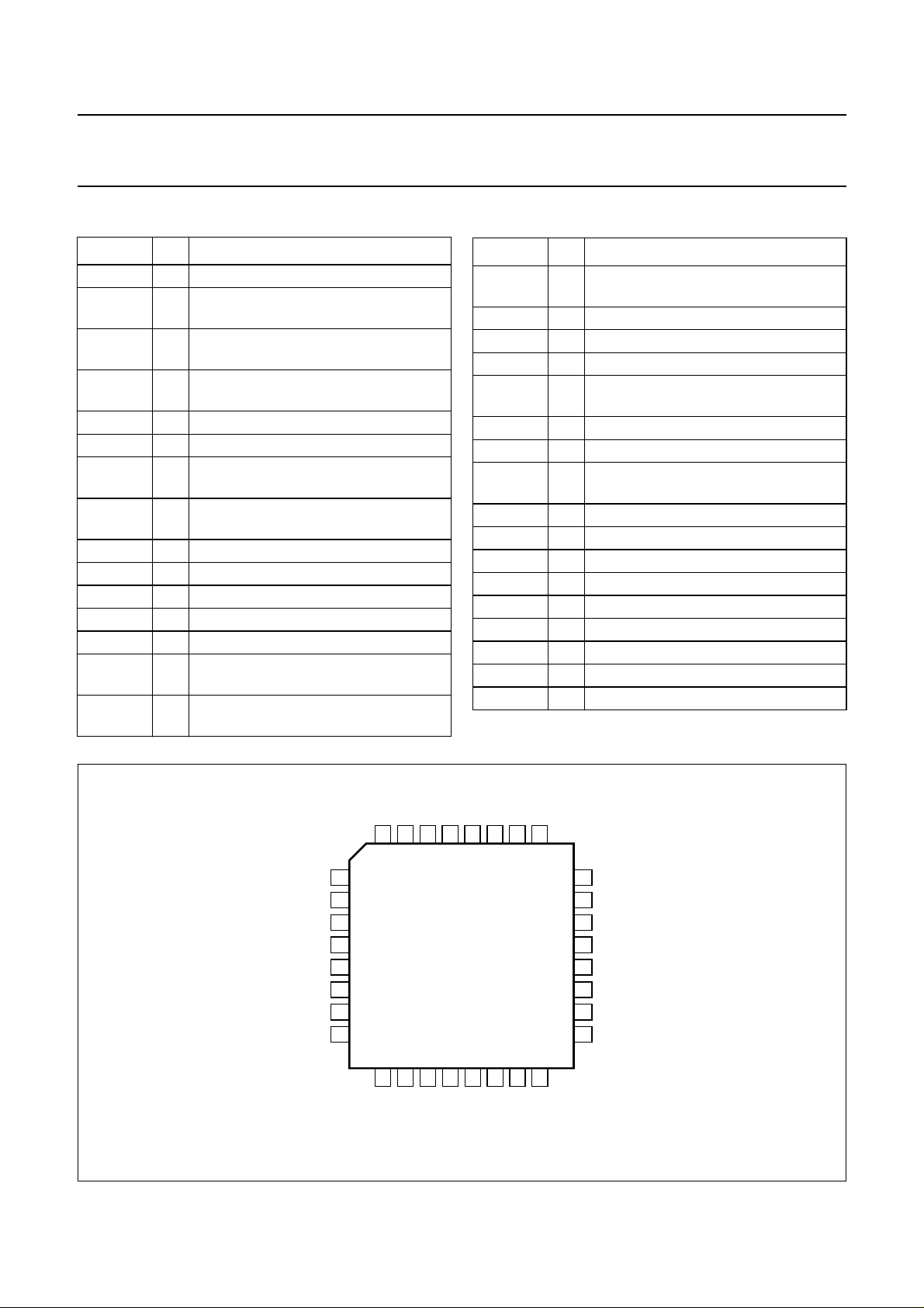
7 PINNING
SYMBOL PIN DESCRIPTION
ATL 1 alert LOW level output
ALC 2 alert control input (normally LOW by
internal pull-down)
DON 3 direct ON/OFF input (normally LOW by
internal pull-down)
REF 4 real-time clock frequency reference
output
INT 5 interrupt output
n.c. 6 not connected
RST 7 reset input (normally LOW by internal
pull-down)
V
PR
SDA 9 I
SCL 10 I
V
DD
V
SS
V
PO
CCP 14 voltage converter shunt capacitor
CCN 15 voltage converter shunt capacitor
8 external positive voltage reference
input
2
C-bus serial data input/output
2
C-bus serial clock input
11 main positive supply voltage
12 main negative supply voltage
13 voltage converter positive output
(positive side)
(negative side)
PCD5002A
SYMBOL PIN DESCRIPTION
TS1 16 test input1 (normally LOW by internal
pull-down)
XTAL2 17 decoder crystal oscillator output
XTAL1 18 decoder crystal oscillator input
n.c. 19 not connected
TS2 20 test input2 (normally LOW by internal
pull-down)
BAT 21 battery sense input
DQC 22 demodulator quick charge output
RDI 23 received data input (POCSAG or
APOC1)
RXE 24 receiver circuit enable output
ROE 25 receiver oscillator enable output
ZSD 26 synthesizer serial data output
ZSC 27 synthesizer serial clock output
ZLE 28 synthesizer latch enable output
V
SS
VIB 30 vibrator motor drive output
LED 31 LED drive output
ATH 32 alert HIGH level output
29 main negative supply voltage
handbook, full pagewidth
ATL
ALC
DON
REF
INT
n.c.
RST
V
PR
1
2
3
4
5
6
7
8
ATH
32
9
SDA
LED
VIB
31
30
PCD5002AH
10
11
DD
SCL
V
V
Fig.2 Pin configuration.
1999 Jan 08 5
29
12
V
SS
SS
ZLE
28
13
PO
V
ZSC
27
14
CCP
ZSD
26
15
CCN
ROE
25
16
TS1
24
23
22
21
20
19
18
17
MGL564
RXE
RDI
DQC
BAT
TS2
n.c.
XTAL1
XTAL2

Philips Semiconductors Product specification
Enhanced Pager Decoder for
APOC1/POCSAG
8 FUNCTIONAL DESCRIPTION
8.1 Introduction
The PCD5002A is a very low power decoder and pager
controller specifically designed for use in new generation
radio pagers. The architecture of the PCD5002A allows for
flexible application in a wide variety of radio pager designs.
The PCD5002A is fully compatible with
paging Code No. 1”
operating at data rates of 512, 1200 and 2400 bits/s using
a single oscillator crystal of 76.8 kHz.
The PCD5002A also supports the new Advanced Pager
Operator’s Code Phase 1 (APOC1). This compatible
extension to the POCSAG code improves battery
economy by introducing ‘cycles’ and batch numbering.
A cycle consists of 5 or 15 standard POCSAG batches.
Each pager will be allocated a batch number in addition to
its POCSAG address and it will only search for its address
during this batch.
In addition to the standard POCSAG sync word (used also
in APOC1) the PCD5002A is also capable of recognizing
up to 4 User Programmable Sync Words (UPSWs).
This permits the reception of both private services and
POCSAG or APOC1 transmissions via the same radio
channel. As an option reception of a UPSW may activate
Continuous Data Decoding (CDD).
Used together with the Philips UAA2080 or UAA2082
paging receiver, the PCD5002A offers a highly
sophisticated, miniature solution for the radio paging
market. Control of an RF synthesizer circuit is also
provided to ease alignment and channel selection.
On-chip EEPROM provides storage for user addresses
(Receiver Identity Codes or RICs) and Special
Programmed Functions (SPFs) and UPSWs, which
eliminates the need for external storage devices and
interconnection. For other non-volatile storage 20 bytes of
general purpose EEPROM are available. The low
EEPROM programming voltage makes the PCD5002A
well suited for ‘over-the-air’ programming/reprogramming.
On request from an external controlling device or
automatically (by SPF programming), the PCD5002A will
provide standard POCSAG alert cadences by driving a
standard acoustic ‘beeper’. Non-standard alert cadences
may be generated via a cadence register or a dedicated
control input.
The PCD5002A can also produce a HIGH level acoustic
alert as well as drive an LED indicator and a vibrator motor
via external bipolar transistors.
(also known as the POCSAG code)
“CCIR Radio
PCD5002A
The PCD5002A contains a low-power, high-efficiency
voltage converter (doubler) designed to provide a higher
voltage supply to LCD drivers or microcontrollers.
In addition, an independent level shifted interface is
provided allowing communication to a microcontroller
operating at a higher voltage than the PCD5002A.
Interface to such an external device is provided by an
2
I
C-bus which allows received call identity and message
data, data for the programming of the internal EEPROM,
alert control and pager status information to be transferred
between the devices. Pager status includes features
provided by the PCD5002A such as battery-low and
out-of-range indications. A dedicated interrupt line
minimizes the required microcontroller activity.
A selectable low frequency timing reference is provided for
use in real-time clock functions.
Data synchronization is achieved by the Philips patented
ACCESS algorithm ensuring that maximum advantage is
made of the POCSAG code structure particularly in fading
radio signal conditions. The algorithm allows for data
synchronization without preamble detection whilst
minimizing battery power consumption. The APOC1 code
uses an extended version of the ACCESS
synchronization algorithm.
Random (and optional) burst error correction techniques
are applied to the received data to optimize the call
success rate without increasing the falsing rate beyond
specified POCSAG levels.
8.2 The POCSAG paging code
A transmission using the
(POCSAG code) is constructed in accordance with the
following rules (see Fig.3).
The transmission is started by sending a preamble,
consisting of at least 576 continuously alternating bits
(10101010...). The preamble is followed by an arbitrary
number of batch blocks. Only complete batches are
transmitted.
Each batch comprises 17 code-words of 32 bits each.
The first code-word is a synchronization code-word with a
fixed pattern. The sync word is followed by 8 frames
(0 to 7) of 2 code-words each, containing message
information. A code-word in a frame can either be an
address, message or idle code-word.
Idle code-words also have a fixed pattern and are used to
fill empty frames or to separate messages.
“CCIR Radio paging Code No. 1”
1999 Jan 08 6
Philips Semiconductors Product specification
Enhanced Pager Decoder for
APOC1/POCSAG
Address code-words are identified by an MSB at logic 0
and are coded as shown in Fig.3. A user address or RIC
consists of 21 bits. Only the upper 18 bits are encoded in
the address code-word (bits 2 to 19). The lower 3 bits
designate the frame number (0 to 7) in which the address
is transmitted.
Four different call types (‘numeric’, ‘alphanumeric’ and two
‘alert only’ types) can be distinguished. The call type is
determined by two function bits in the address code-word
(bits 20 and 21), as shown in Table 1.
Alert-only calls consist only of a single address code-word.
Numeric and alphanumeric calls have message
code-words following the address. A message causes the
frame structure to be temporarily suspended. Message
code-words are sent until the message is completed, with
only the sync words being transmitted in their expected
positions.
Message code-words are identified by an MSB at logic 1
and are coded as shown in Fig.3. The message
information is stored in a 20-bit field (bits 2 to 21).
PCD5002A
This permits correction of a maximum of 2 random errors
or up to 3 errors in a burst of 4 bits (a 4-bit burst error) per
code-word.
8.3 The APOC1 paging code
The APOC1 paging code is fully POCSAG compatible and
involves the introduction of batch grouping and a Batch
Zero Identifier (BZI). This reserved address code-word
indicates the start of a ‘cycle’ of 5 or 15 batches long and
is transmitted immediately after a sync word.
Cycle transmission must be coherent i.e. a transmission
starting an integer number of cycle periods after the start
of the previous one.
Broadcast message data may be included in a
transmission. This information may occupy any number of
message code-words and immediately follows the batch
zero identifier of the first cycle after preamble.
The presence of data is indicated by the function bits in the
batch zero identifier: 1,1 indicates ‘no broadcast data’.
Any other combination indicates a broadcast message.
The standard data format is determined by the call type:
4 bits per digit for numeric messages and 7 bits per
(ASCII) character for alphanumeric messages.
Each code-word is protected against transmission errors
by 10 CRC check bits (bits 22 to 31) and an even-parity bit
(bit 32).
handbook, full pagewidth
PREAMBLE BATCH 1 BATCH 2 BATCH 3 LAST BATCH
10101 . . . 10101010
SYNC | CW CW | CW CW | . . . . . | CW CW
Address code-word
0 18-bit address 2 function bits 10 CRC bits P
The PCD5002A can be configured for POCSAG or
APOC1 operation via SPF programming. The batch zero
identifier is programmable and can be stored in any
identifier location in EEPROM.
The POCSAG standard only allows combinations of data
formats and function code bits as given in Table 1.
However, other (non-standard) combinations will be
decoded normally by the PCD5002A.
FRAME 0 FRAME 1 FRAME 7
Message code-word
1 20-bit message 10 CRC bits P
Fig.3 POCSAG code structure.
1999 Jan 08 7
MCD456

Philips Semiconductors Product specification
Enhanced Pager Decoder for
APOC1/POCSAG
Table 1 POCSAG recommended call types and function bits
BIT 20 (MSB) BIT 21 (LSB) CALL TYPE DATA FORMAT
0 0 numeric 4-bits per digit
0 1 alert only 1 −
1 0 alert only 2 −
1 1 alphanumeric 7-bits per ASCII character
8.4 Error correction
In the PCD5002A error correction methods have been
implemented as shown in Table 2.
Random error correction is default for both address and
message code-words. In addition, burst error correction
can be enabled by SPF programming. Up to 3 erroneous
bits in a 4-bit burst can be corrected.
The error type detected for each code-word is identified in
the message data output to the microcontroller, allowing
rejection of calls with too many errors.
Table 2 Error correction
ITEM CORRECTION
Preamble 4 random errors in 31 bits
Synchronization
code-word
Address code-word 2 random errors; plus 4-bit burst
Message code-word 2 random errors; plus 4-bit burst
8.5 Operating states
The PCD5002A has 2 operating states:
• ON status
• OFF status.
The operating state is determined by a direct control input
(DON) and bit D4 in the control register (see Table 3).
Table 3 Truth table for decoder operating status
DON
INPUT
CONTROL
BIT D4
0 0 OFF
01 ON
10 ON
11 ON
2 random errors in 32 bits
errors (optional)
errors (optional)
OPERATING STATUS
PCD5002A
8.6 ON status
In the ON status the decoder pulses the receiver and
oscillator enable outputs (RXE and ROE respectively)
according to the code structure and the synchronization
algorithm. Data received serially at the data input (RDI) is
processed for call reception.
The data protocol can be POCSAG or APOC1.
Continuous data decoding upon reception of a special
sync word is also supported. The data protocol is selected
by SPF programming.
Reception of a valid paging call is signalled to the
microcontroller by an interrupt signal. The received
address and message data can then be read via the
2
C-bus interface.
I
8.7 OFF status
In the OFF status the decoder will neither activate the
receiver or oscillator enable outputs, nor process any data
at the data input. The crystal oscillator remains active to
permit communication with the microcontroller.
In both operating states an accurate timing reference is
available via the REF output. Using SPF programming the
signal periodicity may be selected as;
32.768 kHz, 50 Hz, 2 Hz or
8.8 Reset
The decoder can be reset by applying a positive pulse on
input pin RST. For successful reset at power-on, a HIGH
level must be present on the RST pin while the device is
powering-up.
This can be applied by the microcontroller, or via a suitable
RC power-on reset circuit connected to the RST input.
Reset circuit details and conditions during and after a reset
are described in Chapter 9.
1
⁄60Hz.
1999 Jan 08 8

Philips Semiconductors Product specification
Enhanced Pager Decoder for
APOC1/POCSAG
8.9 Bit rates
The PCD5002A can be configured for data rates of 512,
1200 or 2400 bits/s by SPF programming. These data
rates are derived from a single 76.8 kHz oscillator
frequency.
8.10 Oscillator
The oscillator circuit is designed to operate at 76.8 kHz.
Typically, a tuning fork crystal will be used as a frequency
source. Alternatively, an external clock signal can be
applied to pin XTAL1 (amplitude = V
slightly higher oscillator current is consumed. A 2.2 MΩ
feedback resistor connected between XTAL1 and XTAL2
is required for proper operation.
To allow easy oscillator adjustment (e.g. by a variable
capacitor) a 32.768 kHz reference frequency can be
selected at output REF by SPF programming.
8.11 Input data processing
Data input is binary and fully asynchronous. Input bit rates
of 512, 1200 and 2400 bits/s are supported. As a
programmable option, the polarity of the received data can
be inverted before further processing.
The input data is noise filtered by a digital filter. Data is
sampled at 16 times the data rate and averaged by
majority decision.
The filtered data is used to synchronize an internal clock
generator by monitoring transitions. The recovered clock
phase can be adjusted in steps of
received bit.
The larger step size is used when bit synchronization has
not been achieved, the smaller when a valid data
sequence has been detected (e.g. preamble or sync
word).
8.12 Battery saving
Current consumption is reduced by switching off internal
decoder sections whenever the receiver is not enabled.
To further increase battery efficiency, reception and
decoding of an address code-word is stopped as soon as
the uncorrected address field differs by more than 3 bits
from the enabled RICs. If the next code-word must be
received again, the receiver is re-enabled thus observing
the programmed establishment times t
to VSS), but a
DD
1
⁄8or1⁄32bit period per
RXE
and t
ROE
.
PCD5002A
The current consumption of the complete pager can be
minimized by separately activating the RF oscillator circuit
(using output ROE) before activating the rest of the
receiver. This is possible using the UAA2082 receiver
which has external biasing for the oscillator circuit.
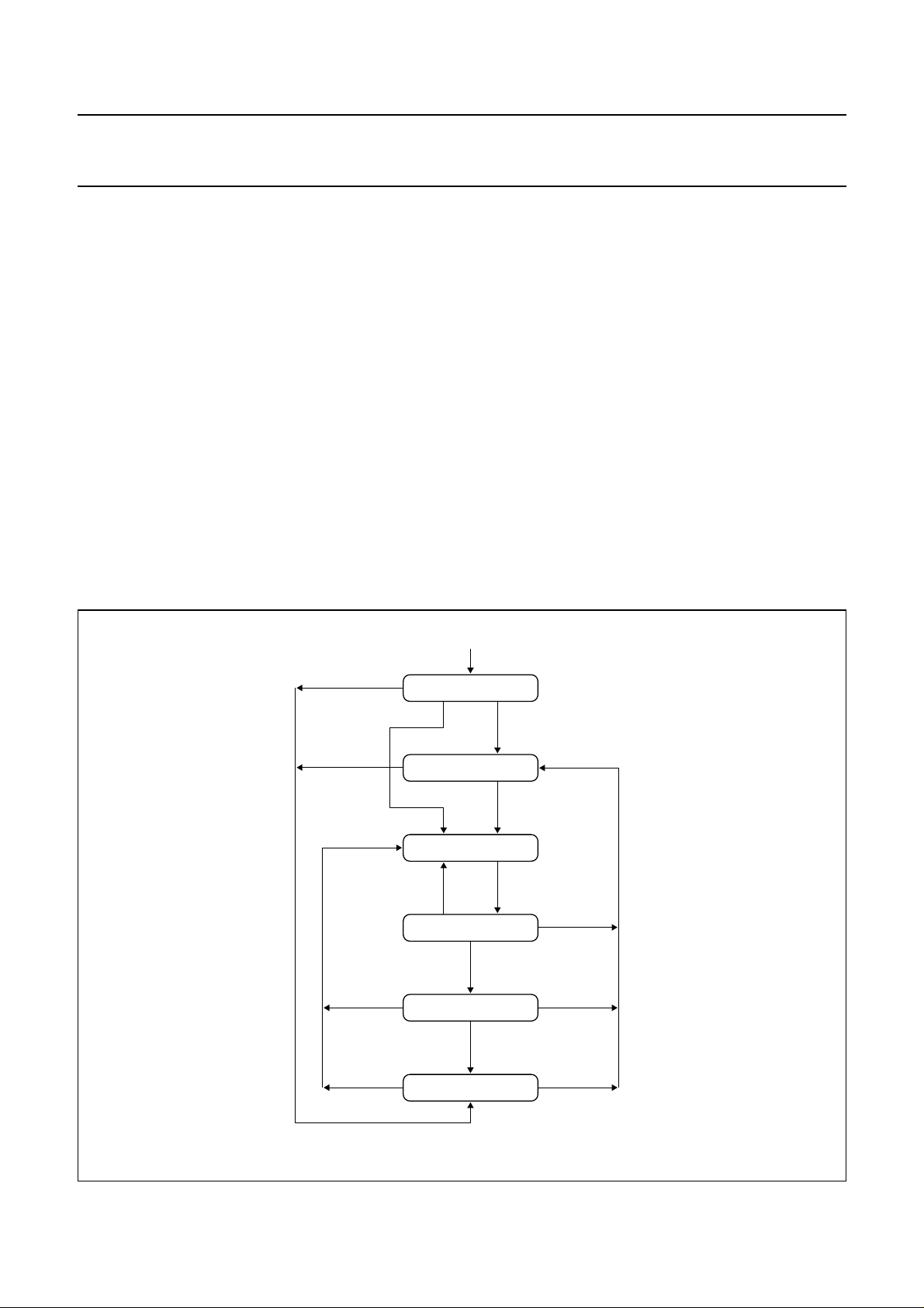
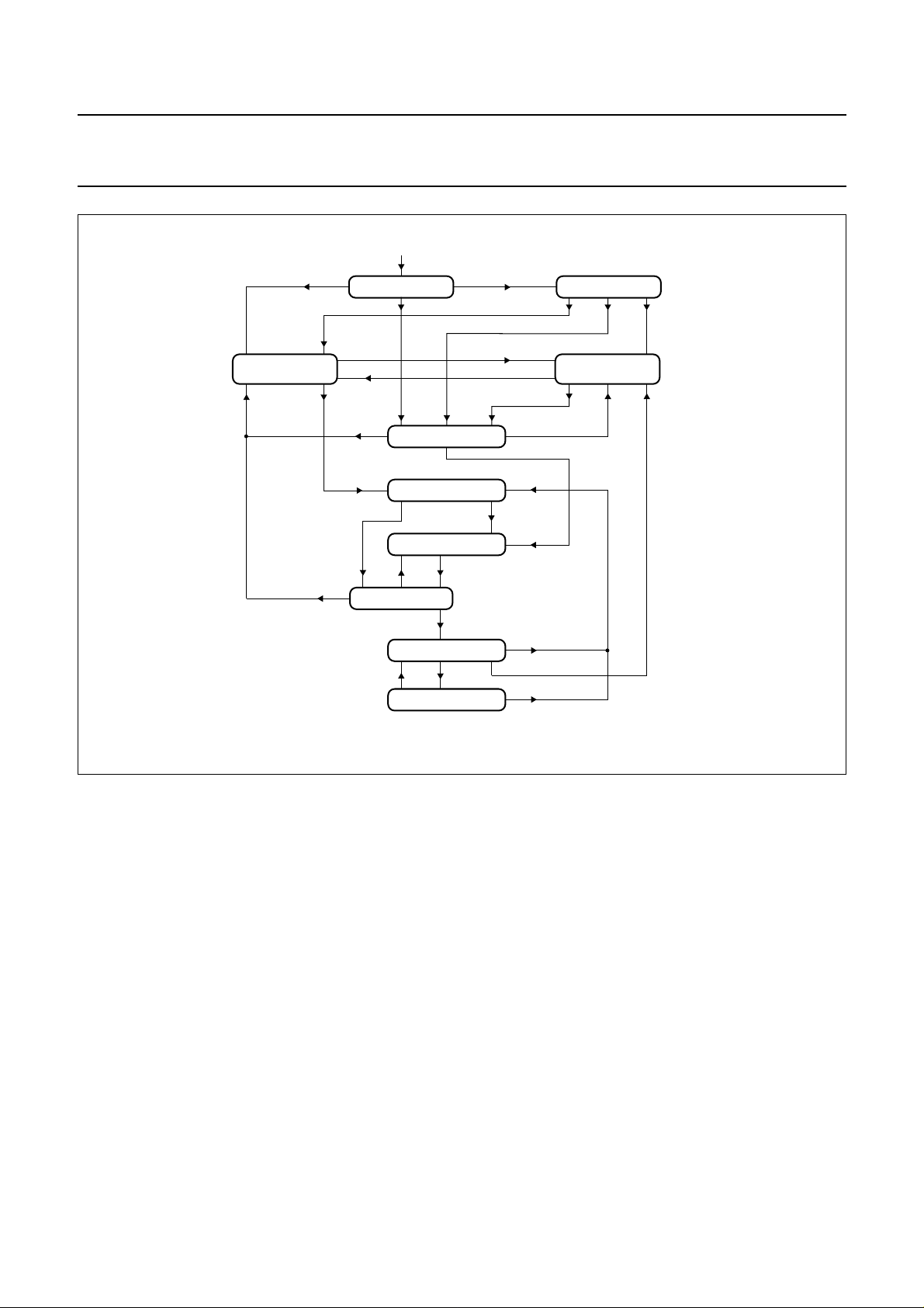
8.13 POCSAG synchronization strategy
In the ON status the PCD5002A synchronizes to the
POCSAG data stream by the Philips ACCESS
A flow diagram is shown in Fig.4. Where ‘sync word’ is
used, this implies both the standard POCSAG sync word
and any enabled User Programmable Sync Word
(UPSW).
Several modes of operation can be distinguished
depending on the synchronization state. Each mode uses
a different method to obtain or retain data synchronization.
The receiver and oscillator enable outputs (RXE and ROE
respectively) are switched accordingly, with the
appropriate establishment times (t
RXON
respectively).
Before comparing received data with preamble, an
enabled sync word or programmed user addresses, the
appropriate error correction is applied.
Initially, after switching to the ON status, the decoder is in
switch-on mode. Here the receiver will be enabled for a
period up to 3 batches, testing for preamble and the sync
word. Failure to detect preamble or the sync word will
cause the device to switch to the ‘carrier off’ mode.
When preamble is detected it will cause the device to
switch to the preamble receive mode, in which a sync
word is searched for. The receiver will remain enabled
while preamble is detected. When neither sync word nor
preamble is found within a 1 batch duration the ‘carrier off’
mode is entered.
Upon detection of a sync word the data receive mode is
entered. The receiver is activated only during enabled user
address frames and sync word periods. When an enabled
user address has been detected, the receiver will be kept
enabled for message code-word reception until the call
termination criteria are met.
During call reception data bytes are stored in an internal
SRAM buffer, capable of storing 2 batches of message
data.
Messages are transmitted contiguously, only interrupted
by sync words at the beginning of each batch.
and t
algorithm.
ROON
1999 Jan 08 9
Philips Semiconductors Product specification
Enhanced Pager Decoder for
APOC1/POCSAG
When a message extends beyond the end of a batch no
testing for sync takes place. Instead, a message data
transfer will be initiated by an interrupt to the external
controller. Data reception continues normally after a period
corresponding to the sync word duration.
If any message code-word is found to be uncorrectable,
the ‘data fail’ mode is entered and no data transfer will be
attempted at the next sync word position. Instead, a test for
sync word will be carried out.
In the data fail mode message reception continues
normally for 1 batch duration. When a sync word is
detected at the expected position the decoder returns to
the ‘data receive’ mode. If the sync word again fails to
appear, then batch synchronization is deemed lost. Call
reception is then terminated and the ‘fade recovery’ mode
is entered.
Thefade recovery mode is intended to scan for sync word
and preamble over an extended window (nominal
position ± 8 bits). This is performed for a period of up to
PCD5002A
15 batches, allowing recovery of synchronization from
long fades in the radio signal. Detection of preamble
causes switching to the ‘preamble receive’ mode, while
sync word detection causes switching to the ‘data receive’
mode. When neither is found within a period of 15 batches,
the radio signal is considered lost and the ‘carrier off’ mode
is entered.
The purpose of the carrier off mode is to detect a valid
radio transmission and synchronize to it quickly and
efficiently. Because transmissions may start at random,
the decoder enables the receiver for 1 code-word in every
18 code-words looking for preamble or sync word.
By using a buffer containing 32 bits (n bits from the current
scan, 32 − n from the previous scan) effectively every
batch bit position can be tested within a continuous
transmission of at least 18 batches. Detection of preamble
causes the device to switch to the ‘preamble receive’
mode, while sync word detection causes the device to
switch to the ‘data receive’ mode.
handbook, full pagewidth
no preamble or
sync word
(3 batches)
no preamble or
sync word
(1 batch)
sync word
OFF to ON status
switch-on
preamble receive
data receive
data fail
no preamble or
sync word
(1 batch)
fade recovery
no preamble or
sync word
(15 batches)
carrier off
preamble
sync word
no sync wordsync word
preamble
preamblesync word
preamblesync word
MLC247
Fig.4 ACCESS synchronization algorithm for POCSAG.
1999 Jan 08 10
Philips Semiconductors Product specification
Enhanced Pager Decoder for
APOC1/POCSAG
handbook, full pagewidth
preamble
preamble receive 1
sync word
preamble
no batch zero ID
preamble
no preamble
OFF to ON status
sync word
preamble
batch zero detect
batch zero ID
batch zero identify
cycle receive
sync
word
short fade recovery
transmitter off
(1 batch)
preamble receive 2
no preamble
or sync word
(3 batches)
preamble
no preamble (1 batch)
sync word
no sync word
batch
zero ID
no sync
word
no sync word
or preamble
preamble
sync word
TX off time out
sync word
carrier detectswitch on
sync word
long fade recovery
MGD269
PCD5002A
TX off
time out
Fig.5 APOC1 synchronization algorithm.
8.14 APOC1 synchronization strategy
The synchronization strategy in APOC1 is an extended
version of the ACCESS scheme and is illustrated in Fig.5.
The PCD5002A counts the number of batches in a
transmission, starting from the first batch received after
preamble. Counter overflow occurs due to the size of a
cycle, as determined by SPF programming.
Initially, after switching to the ON status, the decoder will
be in the switch-on mode. Here the receiver will be
enabled for up to 3 batches, testing for preamble and sync
word. Detection of preamble causes the device to switch
to the ‘preamble receive’ mode, while any enabled sync
word enters the ‘batch zero detect’ mode. Failure to detect
either will cause the device to switch to the ‘carrier detect’
mode.
In thepreamble receive 1 mode the PCD5002A searches
for a sync word, the receiver remaining enabled while
preamble is detected. As soon as an enabled sync word is
found the ‘batch zero identify’ mode is started.
If preamble is not found within one batch duration then the
‘long fade recovery’ mode is entered.
When in batch zero detect mode the PCD5002A
switches on every batch to maintain synchronization and
check for the batch zero identifier. Detection of the batch
zero identifier activates the ‘cycle receive’ mode. When
synchronization is lost the ‘long fade recovery’ mode is
entered. ‘preamble receive’ mode is entered when
preamble is detected.
In the batch zero identify mode the first code-word
immediately after the sync word of the first batch is
compared with the programmed batch zero identifier.
Failure to detect the batch zero identifier will cause the
device to enter the ‘short fade recovery’ mode.
When this comparison is successful the function bits
determine whether any broadcast message will follow.
Any function bit combination other than ‘1,1’ will cause the
PCD5002A to accept message code-words until
terminated by a valid address code-word.
1999 Jan 08 11

Philips Semiconductors Product specification
Enhanced Pager Decoder for
APOC1/POCSAG
After reception of any broadcast message data the
PCD5002A continues to operate in the ‘cycle receive’
mode.
In the cycle receive mode the PCD5002A enables call
reception in only one programmed batch per cycle. Sync
word detection takes place from 2 bits before to 2 bits after
the expected sync word position of this batch. If the sync
word is not detected then the position of the current sync
word will be maintained and the ‘short fade recovery’
mode will be entered.
When a valid sync word is found user address code-word
detection takes place, as in normal POCSAG code.
Any following message code-words are received normally.
If a message extends into a subsequent batch containing
a batch zero identifier, then the batch zero identifier is
detected normally and message reception will continue.
Data reception is suspended after the programmed batch
until the same batch position in the next cycle.
The exception being when a received call continues into
the next batch.
In the short fade recovery mode the programmed data
receive batch will continue to be checked for user address
code-words. In addition the first code-word after the
programmed batch is checked for sync word or preamble.
When a valid sync word is detected the ‘cycle receive’
mode is re-entered, while detection of preamble causes
the device to switch to the ‘preamble receive’ mode. When
neither is found then the ‘transmitter off’ mode is entered.
In the transmitter off mode a time-out is set to a
pre-programmed duration. This time-out corresponds to
the maximum time between subsequent transmissions
(preamble to preamble).
The PCD5002A then checks the first batch of every cycle
for sync word or preamble. The programmed data receive
batch is ignored (unless it is batch 0).
Table 4 Synchronization window tolerance as a function
of bit rate
TIME FROM LOSS
OF SIGNAL
(bits/s)
≤30 s 4 bits 4 bits 4 bits
≤60 s 4 bits 4 bits 8 bits
≤120 s 4 bits 8 bits 16 bits
≤240 s 8 bits 16 bits 32 bits
512
TOLERANCE
1200
(bits/s)
2400
(bits/s)
PCD5002A
Synchronization checking is performed over a window
ranging from ‘n’ bits before to ‘n’ bits after the expected
sync word position. The window tolerance ‘n’ depends on
the time since the ‘transmitter off’ mode was entered and
on the selected bit rate (see Table 4).
When a sync word is detected in this widened
synchronization window the PCD5002A enters the
‘batch zero identify’ mode. Time-out expiry before a sync
word has been detected causes the device to switch to the
‘long fade recovery’ mode.
Detection of preamble in the ‘transmitter off’ mode initiates
the preamble receive 2 mode. Operation in this mode is
identical to ‘preamble receive mode’. Failure to detect
preamble for one batch period will cause the device to
switch back to the ‘transmitter off’ mode. This prevents
inadvertent loss of cycle synchronization due to spurious
signals resembling preamble.
The carrier detect mode is identical to the ‘carrier off’
mode in standard POCSAG operation. Upon first entry the
transmitter off time-out is started. The receiver is enabled
to receive one code-word in every 18 code-words to check
for sync word and preamble. This check is performed on
the last available 32 bits for every received bit.
The ‘preamble receive’ mode is entered if preamble is
detected. If a valid sync word is found the
‘batch zero detect’ mode is entered. If neither has been
detected and the time-out expires, then the
‘long fade recovery’ mode is entered.
The long fade recovery mode is intended to quickly
regain synchronization in fading conditions (not caused by
the transmitter switching off between transmissions) or
when having been out of range, while maintaining
acceptable battery economy.
Initially, the receiver is switched off until one cycle duration
after the last enabling in the ‘transmitter off’ mode.
The receiver is then enabled for a 2 code-word period in
which each contiguous group of 32 bits is tested for any
decodable POCSAG code-word (including sync word)
and preamble. Single-bit error correction is applied.
If a code-word is detected, the receiver enable period is
extended by another code-word duration and the above
test is repeated. This process continues while valid
code-words are received.
1999 Jan 08 12

Philips Semiconductors Product specification
Enhanced Pager Decoder for
APOC1/POCSAG
Detection of preamble will cause the device to switch to the
‘preamble receive’ mode, while sync word detection will
cause the device to switch to the ‘batch zero detect’ mode.
When neither is detected during the 2 code-word window
or any following 32-bit group, the receiver will be disabled.
If valid code-words are detected but no sync word or
preamble is detected over a period of 18 code-words, the
receiver is also disabled.
Data sampling, as previously described, is repeated one
cycle duration after the moment the receiver was last
activated.
8.15 Call termination
Call reception is terminated:
• Upon reception of any address code-word (including idle
code-word but excluding the batch zero identifier in
APOC1 operation) requiring no more than single bit
error correction
• Upon reception of a correctable address code-word
(error type other than ‘111’; see Table 11) that matches
an enabled RIC
• When a forced call termination command is received
from an external controller.
• In ‘data fail’ mode, when a sync word is not detected at
the expected batch position.
The last method permits an external controller to stop call
reception, depending on the number and type of errors
which occurred in a call. After a forced call termination the
decoder will enter the ‘data fail’ mode.
The type of error correction as well as the call termination
conditions are indicated by status bits in the message data
output.
PCD5002A
8.16 Enhanced call termination
The PCD5002A provides an enhanced mode of call
termination which is enabled by setting SPF byte 3, bit D7.
When enabled, the following call termination conditions
applies, in addition to those listed in Section 8.15.
• Reception of two consecutive code-words (excluding
sync word), each of which are either uncorrectable or an
address code-word with more than one bit in error.
8.17 Call data output format
POCSAG call information is stored in the decoder SRAM
in blocks of 3 bytes per code-word. Each stored call
consists of a call header, followed by message data blocks
and a call terminator. In the event of concatenated
messages the call terminator is replaced with the call
header of the next message. An alert-only call only has a
call header and a call terminator.
The formats of a call header, a message data block and a
call terminator are shown in Tables 5, 7 and 9.
A Call Header contains information on the last sync word
received, the RIC which began call reception and the type
of error correction performed on the address code-word.
A Message Data block contains the data bits from a
message code-word plus the type of error correction
performed. No deformatting is performed on the data bits:
numeric data appear as 4-bit groups per digit,
alphanumeric data has a 7-bit ASCII representation.
The Call Terminator contains information on the last sync
word received, information on the way the call was
terminated (forced call termination command, loss of sync
word in ‘data fail’ mode) and the type of error correction
performed on the terminating code-word.
In the event of the terminating code-word matching an
enabled RIC, a concatenated call will be started with the
call header replacing the terminator of the previous call.
Following call termination, transfer of the data received
since the previous sync word period is initiated by an
interrupt to the external controller.
1999 Jan 08 13

Philips Semiconductors Product specification
Enhanced Pager Decoder for
PCD5002A
APOC1/POCSAG
Table 5 Call header format
BYTE NUMBER
1 0 S3 S2 S1 R3 R2 R1 DF
2 0 S3 S2 S1 R3 R2 R1 0
3 X X F0F1E3E2E1 0
Table 6 Call header bit identification
BITS (MSB TO LSB) IDENTIFICATION
S3 to S1 identifier number of sync word for current batch (7 = standard POCSAG)
R3 to R1 identifier number of user address (RIC)
DF data fail mode indication (1 = data fail mode); note 1
F0 and F1 function bits of received address code-word (bits 20 and 21)
E3 to E1 detected error type; see Table 11; E3 = 0 in a concatenated call header
Note
1. The DF bit in the call header is set:
a) When the sync word of the batch in which the (beginning of the) call was received, did not match the standard
POCSAG or a user-programmed sync word. The sync word identifier (bits S3 to S1) will then be made 0.
b) When any code-word of a previous call received in the same batch was uncorrectable.
BIT 7
(MSB)
BIT 6 BIT 5 BIT 4 BIT 3 BIT 2 BIT 1
BIT 0
(LSB)
Table 7 Message data format
BYTE NUMBER
1 M2M3M4M5M6M7M8M9
2 M10 M11 M12 M13 M14 M15 M16 M17
3 M18 M19 M20 M21 E3 E2 E1 M1
Table 8 Message data bit identification
BITS (MSB TO LSB) IDENTIFICATION
M2 to M21 message code-word data bits
E3 to E1 detected error type; see Table 11
M1 message code-word flag
Table 9 Call terminator format
BYTE NUMBER
1 FTS3S2S1 0 0 0 DF
2 FTS3S2S1 0 0 0 X
3 XXXXE3E2E10
BIT 7
(MSB)
BIT 7
(MSB)
BIT 6 BIT 5 BIT 4 BIT 3 BIT 2 BIT 1
BIT 6 BIT 5 BIT 4 BIT 3 BIT 2 BIT 1
BIT 0
(LSB)
BIT 0
(LSB)
1999 Jan 08 14

Philips Semiconductors Product specification
Enhanced Pager Decoder for
PCD5002A
APOC1/POCSAG
Table 10 Call terminator bit identification
BITS (MSB TO LSB) IDENTIFICATION
FT forced call termination (1 = yes)
S3 to S1 identifier number of last sync word
DF data fail mode indication (1 = data fail mode); note 1
E3 to E1 detected error type; see Table 11; E3 = 0 in a call terminator
Note
1. The DF bit in the call terminator is set:
a) When any call data code-word in the terminating batch was uncorrectable, while in ‘data receive’ mode.
b) When the sync word at the start of the terminating batch did not match the standard POCSAG or a
user-programmed sync word, while in ‘data fail’ mode.
Table 11 Error type identification (note 1)
E3 E2 E1
0 0 0 no errors; correct code-word 0
0 0 1 parity bit in error 1
0 1 0 single bit error 1 + parity
0 1 1 single bit error and parity error 1
1 0 0 not used −
1 0 1 4-bit burst error and parity error 3 (e.g. 1101)
1 1 0 2-bit random error 2
1 1 1 uncorrectable code-word 3 or more
ERROR TYPE
NUMBER OF ERRORS
Note
1. POCSAG code allows a maximum of three bit errors to be detected per code-word.
8.18 Error type indication
Table 11 shows how the different types of detected errors
are encoded in the call data output format.
8.19 Data transfer
Data transfer is initiated either during sync word periods or
as soon as the receiver is disabled after call termination.
If the SRAM buffer is full, data transfer is initiated
immediately during the next code-word.
When the PCD5002A is ready to transfer received call
data an external interrupt will be generated via output INT.
Any message data can be read by accessing the RAM
output register via the I
output starting from the position indicated by the RAM read
pointer.
Call termination can occur on reception of an address
code-word (or even a message code-word if in Enhanced
Call Termination Mode) or when a sync word is not
2
C-bus interface. Bytes will be
detected while in the ‘Data Fail’ mode (‘Short Fade
Recovery’ in APOC1).
8.20 Continuous data decoding
Apart from transmissions in the POCSAG or APOC1
format, the PCD5002A is also capable of decoding
continuous transmissions with the same code-word
structure. Any User-Programmable Sync Word (UPSW)
may be designated to enable continuous data decoding.
When a Continuous Data Decoding (CDD) sync word is
detected at any sync word position, the receiver remains
enabled from then on. Status bits D1 and D0 show the
CDD mode to be active.
All code-words are decoded and their data fields are
stored in SRAM. The usual error information is appended.
No distinction is made between address and message
code-words: code-word bit 0 is treated as a data bit and is
stored in bit M1 of the 3-byte output format.
1999 Jan 08 15
 Loading...