

Philips pcd3360 DATASHEETS

INTEGRATED CIRCUITS
DATA SH EET
PCD3360
Programmable multi-tone
telephone ringer
Product specification
Supersedes data of August 1985
File under Integrated Circuits, IC03
1997 Jan 15

Philips Semiconductors Product specification
Programmable multi-tone telephone ringer PCD3360
CONTENTS
1 FEATURES
2 GENERAL DESCRIPTION
3 QUICK REFERENCE DATA
4 ORDERING INFORMATION
6 PINNING INFORMATION
6.1 Pinning
6.2 Pin description
7 FUNCTIONAL DESCRIPTION
7.1 Supply pins (VDD and VSS)
7.2 Oscillator (OSC)
7.3 Selection pin input circuit)
7.4 Frequency discriminator circuit (FDE and FDI)
7.5 Selection of frequency discriminator limits
(FL and FH)
7.6 Selection of tone sequences (TS1 and TS2)
7.7 Selection of repetition rates (RR1 and RR2)
7.8 Drive mode selection (DM)
7.8.1 Loudspeaker mode
7.8.2 PXE mode
7.9 Setting of impedance, sound pressure level
and automatic swell (IS1 and IS2)
7.10 Optical output (OPT)
8 LIMITING VALUES
9 HANDLING
10 DC CHARACTERISTICS
11 AC CHARACTERISTICS
12 APPLICATION INFORMATION
13 PACKAGE OUTLINES
14 SOLDERING
14.1 Introduction
14.2 DIP
14.2.1 Soldering by dipping or by wave
14.2.2 Repairing soldered joints
14.3 SO
14.3.1 Reflow soldering
14.3.2 Wave soldering
14.3.3 Repairing soldered joints
16 LIFE SUPPORT APPLICATIONS
1997 Jan 15 2
Philips Semiconductors Product specification
Programmable multi-tone telephone ringer PCD3360
1 FEATURES
• Output signals for electro-dynamic transducer
(loudspeaker) or for piezo-electric transducer (PXE)
• 7 basic output frequencies (tones) and a pause
• 4 selectable tone sequences
• 4 selectable repetition rates
• 3 selectable impedance settings
2 GENERAL DESCRIPTION
The PCD3360 is a CMOS integrated circuit, designed to
replace the electro-mechanical bell in telephone sets.
It meets most postal requirements, with selectivity of
output tone sequences and input ringer frequencies.
Output signals for a loudspeaker or for a piezo-electric
(PXE) transducer are provided. No audio transformer is
required since the loudspeaker is driven in class D.
• 3-step automatic swell
• Delta-modulated output signal that approximates a
sinewave
• Input ringing frequency discriminator with selectable
upper and lower frequency limits
• Output for optical signal
• Customized tone sequences, impedance settings and
automatic swell levels are mask programmable.
3 QUICK REFERENCE DATA
SYMBOL PARAMETER CONDITIONS VALUE UNIT
f
TONE
n
int
available frequencies
(tones)
number of intervals per tone
553, 600, 667, 800, 1000, 1067,
1333
15 or 16
Hz
sequence
f
LL
lower limits of frequency
13.33 or 20 Hz
discriminator
f
UL
upper limits of frequency
30 or 60 Hz
discriminator
Z
set
t
d(on)
impedance settings with 50 Ω loudspeaker ≈7, ≈10.5 or ≈17.5 kΩ
switch-on delay ringer frequency = 25 Hz 60 (maximum) ms
4 ORDERING INFORMATION
TYPE
NUMBER
NAME DESCRIPTION VERSION
PACKAGE
PCD3360P DIP16 plastic dual in-line package; 16 leads (300 mil) SOT38-4
PCD3360T SO16 plastic small outline package; 16 leads; body width 7.5 mm SOT162-1
1997 Jan 15 3
Philips Semiconductors Product specification
Programmable multi-tone telephone ringer PCD3360
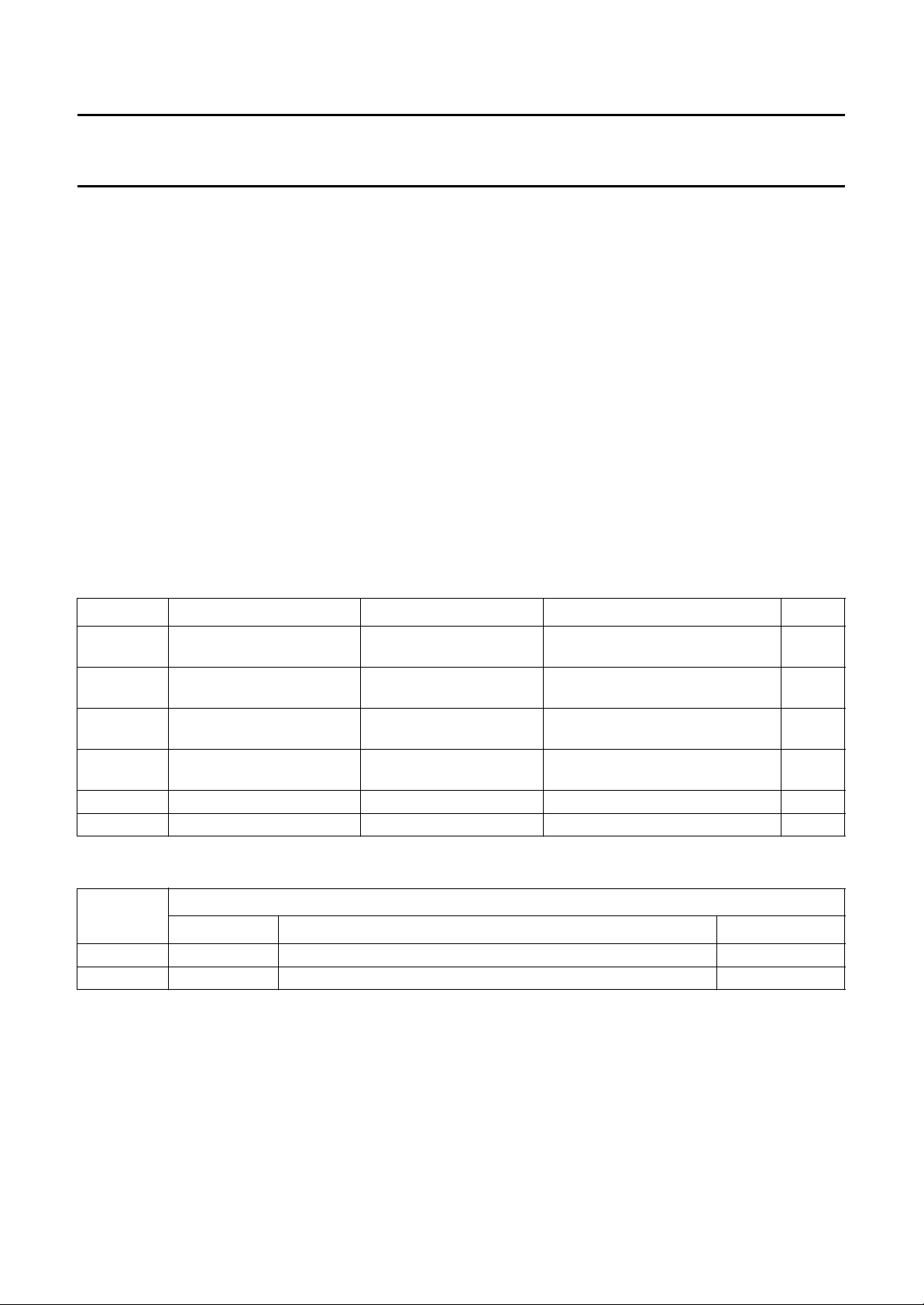
5 BLOCK DIAGRAM
handbook, full pagewidth
4
OSC
OSCILLATOR
(64 kHz)
PCD3360
6 PINNING INFORMATION
6.1 Pinning
f
= 32 kHz
clk
V
DD
V
SS
TONE GENERATION
TONE SEQUENCE GENERATION
TIMING
DUTY CYCLE
CONTROL
101159 14 15 16
IS1 IS2 RR1 RR2 TS1 TS2 DM FDI
3 2 13 12 8
(tone pattern)
(32 kHz pulses)
OUTPUT
CIRCUIT
ENABLE
CIRCUIT
FL FH
6
7
1
TONE
OPT
FDE
MGD710
Fig.1 Block diagram.
6.2 Pin description Table 1 Pin description, PCD3360
handbook, halfpage
FDE
RR2
RR1
OSC
V
DD
TONE
OPT
DM
1
2
3
4
PCD3360P
PCD3360T
5
6
7
8
MGD708
FH
16
FL
15
14
FDI
13
TS1
12
TS2
11
V
SS
10
IS1
9
IS2
Fig.2 Pin configuration.
1997 Jan 15 4
SYMBOL PIN TYPE DESCRIPTION
FDE 1 I frequency discriminator
enable
RR2, RR1 2, 3 I repetition rate selection
OSC 4 I oscillator
V
DD
5 P positive supply
TONE 6 O tone output
OPT 7 O optical signal output
DM 8 I drive mode selection
IS2, IS1 9, 10 I impedance setting and
automatic swell
V
SS
11 P ground
TS2, TS1 12, 13 I tone sequence selection
FDI 14 I frequency discriminator
input
FL, FH 15, 16 I lower and upper
frequency limit selection
Philips Semiconductors Product specification
Programmable multi-tone telephone ringer PCD3360
7 FUNCTIONAL DESCRIPTION (see Fig.1)
7.1 Supply pins (V
If the supply current (V
(V
), the oscillator and most other functions are switched
stb
and VSS)
DD
) drops below the standby voltage
DD
off and the supply current is reduced to the standby current
(I
). The automatic swell register retains its information
stb
until VDD drops further to a value VAS at which reset
occurs.
7.2 Oscillator (OSC)
The 64 kHz oscillator is operated via an external resistor
and capacitor connected to pin OSC (see Fig.8).
The oscillator signal is divided by two to provide the32 kHz
internal system clock.
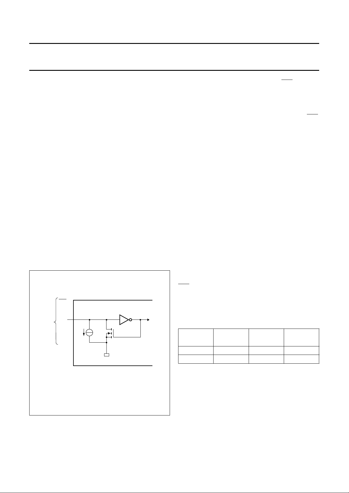
7.3 Selection pin input circuit (see Fig.3) Pins FDE, RR1, RR2, DM, IS1, IS2, TS1, TS2, FL and FH
are pulled down internally by a pull-down current I
when
IH
they are connected to VDD and by a pull-down resistance
RIL when they are connected to VSS. Thus when the pins
are open-circuit they are defined LOW. Therefore only a
single-contact switch is required to connect the pins to
VDD; yet the supply current is only marginally increased as
IIH is very small.
7.4 Frequency discriminator circuit (FDE and FDI)
The frequency discriminator circuit prevents the ringer
being activated unintentionally by dial pulses, speech or
other invalid signals.
The circuit is enabled or disabled by input FDE. WhenFDE
is LOW and VDD>V
, the circuit is enabled and FDI acts
stb
as the input for ringing frequency detection. When FDE is
HIGH, the circuit is disabled and FDI becomes the
enable/disable input for tone sequence generation.
When the circuit is enabled, it starts to produce output
ringing tones after one cycle of an appropriate input
frequency is detected at FDI. An input cycle is detected
when either 2 rising or 2 falling edges are received, and
this implies a delay of between 1 and 1.5 input cycles
before output ringing begins. The allowed input frequency
range is set by the states of pins FL and FH, as shown in
Table 2. Output ringing continues for as long as valid input
ringing frequency is detected.
FDI has a Schmitt-trigger action; the levels are set by an
external resistor R2 (see Fig.8) and an internal sink current
that is switched from 20µA (typ.) for FDI = LOW to <0.1 µA
for FDI = HIGH. Excess current entering FDI via R2 is
absorbed by internal diodes clamped to V
and VSS.
DD
7.5 Selection of frequency discriminator limits (FL and FH)
FDE
RR1
RR2
pins
DM
IS1
IS2
TS1
TS2
FL
FH
I
IH
(1)
PCD3360
V
SS
selection
(1) Transistor resistance is RIL when switched on.
Fig.3 Input circuit of selection pins.
MGD709
With the frequency discriminator enabled (V
DD>Vstb
and
FDE = LOW) the lower and upper limits of the input
frequency are set by the inputs FL and FH as shown by
Table 2.
Table 2 Selection of lower and upper frequency
discriminator limits (f
FL INPUT
STATE
LOWER
LIMIT
= 64 kHz)
OSC
FH INPUT
STATE
UPPER
LIMIT
LOW 20 Hz LOW 60 Hz
HIGH 13.3 Hz HIGH 30 Hz
1997 Jan 15 5
Philips Semiconductors Product specification
Programmable multi-tone telephone ringer PCD3360
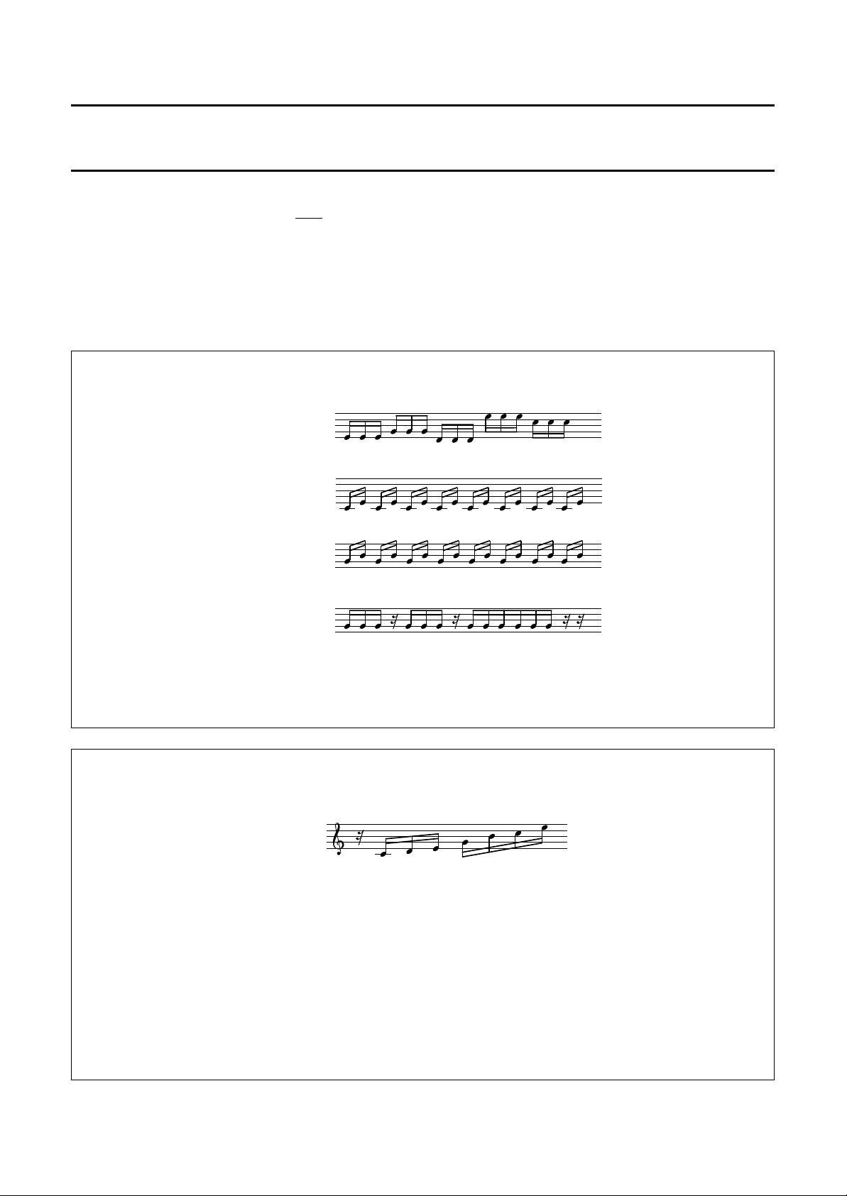
7.6 Selection of tone sequences (TS1 and TS2)
TS1 and TS2 are effective when both FDE and FDI are HIGH, and VDD>V
. TS1 and TS2 normally select one of the
stb
four standard tone sequences shown in Fig.4. Different tone sequences of 15 or 16 consecutive tones and pauses can
be mask programmed to order. The seven tones (plus pause) available are shown in Fig.5, together with the
corresponding ROM codes.
The tone sequences are repeated continuously provided the enable conditions at inputs FDE and FDI are valid and
VDD>V
handbook, full pagewidth
. The first sequence and subsequent repetitions always begin with the first note in the sequence.
stb
pin state
TS1TS2
LL
tone code
HL
tone code
LH
tone code
HH
tone sequence output at pin TONE
3
33
131 131313 31313 31
454 454545 54545 54
222444 777666
handbook, full pagewidth
tone code
444 404044 4444400
MGD715
Fig.4 Tone sequences mask-programmed in the PCD3360.
tone key − cdegbce
frequency (Hz) 5330
frequency ratio 8 9 10 12 15 16 20::::::
tone code 1 2 3 4 5 6 7
0
600 667 800 1000 1067 1333
MGD714
Fig.5 Available tones (including pause) and their corresponding ROM codes.
1997 Jan 15 6
 Loading...