


查询PCA3351C供应商
INTEGRATED CIRCUITS
DATA SH EET
PCA3351C; 52C; 53C;
PCD3351A; 52A; 53A
8-bit microcontrollers with DTMF
generator and 128 bytes EEPROM
Product specification
Supersedes data of 1996 Dec 18
File under Integrated Circuits, IC03
1999 Oct 28

Philips Semiconductors Product specification
8-bit microcontrollers with DTMF generator
and 128 bytes EEPROM
CONTENTS
1 FEATURES
2 GENERAL DESCRIPTION
3 ORDERING INFORMATION
4 BLOCK DIAGRAM
5 PINNING INFORMATION
5.1 Pinning
5.2 Pin description
6 FREQUENCY GENERATOR
6.1 Frequency generator derivative registers
6.2 Melody output (P1.7/MDY)
6.3 Frequency registers
6.4 DTMF frequencies
6.5 Modem frequencies
6.6 Musical scale frequencies
7 EEPROM AND TIMER 2 ORGANIZATION
7.1 EEPROM registers
7.2 EEPROM latches
7.3 EEPROM flags
7.4 EEPROM macros
7.5 EEPROM access
7.6 Timer 2
8 DERIVATIVE INTERRUPTS
9 TIMING
10 RESET
11 IDLE MODE
12 STOP MODE
13 INSTRUCTION SET RESTRICTIONS
14 OVERVIEW OF PORT AND
15 SUMMARY OF DERIVATIVE REGISTERS
16 HANDLING
17 LIMITING VALUES
18 DC CHARACTERISTICS
19 AC CHARACTERISTICS
20 PACKAGE OUTLINES
21 SOLDERING
21.1 Reflow soldering
21.2 Wave soldering
21.3 DIP
21.4 Repairing soldered joints
22 DEFINITIONS
23 LIFE SUPPORT APPLICATIONS
PCA3351C; 52C; 53C;
PCD3351A; 52A; 53A
POWER-ON-RESET CONFIGURATIONS
1999 Oct 28 2

Philips Semiconductors Product specification
8-bit microcontrollers with DTMF generator
and 128 bytes EEPROM
1 FEATURES
• 8-bit CPU, ROM, RAM, EEPROM and I/O; all in one
(28-lead or 32-lead) package
• ROM:
– 2 kbytes (PCA3351C and PCD3351A)
– 4 kbytes (PCA3352C and PCD3352A)
– 6 kbytes (PCA3353C and PCD3353A)
• RAM:
– 64 bytes (PCA3351C and PCD3351A)
– 128 bytes (PCA3352C, PCD3352A, PCA3353C and
PCD3353A)
• 128 bytes Electrically Erasable Programmable
Read-Only Memory (EEPROM)
• Over 100 instructions (based on MAB8048) all of
1 or 2 cycles
• 20 quasi-bidirectional I/O port lines
• 8-bit programmable Timer/event counter 1
• 8-bit reloadable Timer 2
• Three single-level vectored interrupts:
– external
– 8-bit programmable Timer/event counter 1
– derivative; triggered by reloadable Timer 2
• Twotestinputs,oneofwhichalsoservesastheexternal
interrupt input
• DTMF, modem, musical tone generator
• Reference for supply and temperature-independent
tone output
• Filtering for low output distortion (CEPT compatible)
• Melody output for ringer application
• Power-on-reset
• Stop and Idle modes
• Supply voltage: 1.8 to 6 V (DTMF tone output and
EEPROM erase/write from 2.5 V)
• Clock frequency: 1 to 16 MHz (3.58 MHz for DTMF
suggested)
• Operating ambient temperature: −25 to +70 °C or
0to50°C
• Manufactured in silicon gate CMOS process.
PCA3351C; 52C; 53C;
PCD3351A; 52A; 53A
2 GENERAL DESCRIPTION
This data sheet details the specific properties of the
devices referred to. The shared properties of the
PCD33xxA family of microcontrollers are described in the
“PCD33xxA family”
conjunction with this publication.
• ‘PCA3351C; 52C; 53C’ denotes the types PCA3351C,
PCA3352C and PCA3353C. Unless specified, these
types will hereafter be referred to collectively as
‘PCA335xC’.
• ‘PCD3351A; 52A; 53A’ denotes the types PCD3351A,
PCD3352A, PCD3353A. Unless specified, these types
will hereafter be referred to collectively as ‘PCD335xA’.
The PCA335xC and PCD335xA are microcontrollers
designed primarily for telephony applications. They
include an on-chip generator for dual tone multifrequency
(DTMF), modem and musical tones. In addition to dialling,
generated frequencies can be made available as square
waves for melody generation, providing ringer operation.
The PCA335xC and PCD335xA also incorporate
128 bytes of EEPROM, permitting data storage without
battery backup. The EEPROM can be used for storing
telephone numbers, particularly for implementing redial
functions.
The PCA335xC and PCD335xA can be emulated with the
OTP microcontrollers PCD3755A and PCD3755E.
See Chapter 14, Table 25.
The instruction set is similar to that of the MAB8048 and is
a sub-set of that listed in the
sheet.
The differences between PCA335xC and PCD335xA are
shown in Table 1.
Table 1 Differences: PCA335xC and PCD335xA
TYPE V
PCA335xC fixed at 2.0 V ±0.3 V 0 to 50 °C
PCD335xA (1.2 to 3.6 V) ±0.5 V
Note
1. See Chapter 14, Table 26.
data sheet, which should be read in
“PCD33xxA family”
POR
(1)
data
AMBIENT
TEMP. RANGE
−25 to +70 °C
1999 Oct 28 3

Philips Semiconductors Product specification
8-bit microcontrollers with DTMF generator
and 128 bytes EEPROM
3 ORDERING INFORMATION
TYPE
NUMBER
PCA335xCP DIP28 plastic dual in-line package; 28 leads (600 mil) SOT117-1
PCD335xAP
PCA335xCT SO28 plastic small outline package; 28 leads; body width 7.5 mm SOT136-1
PCD335xAT
PCA335xCH LQFP32 plastic low profile quad flat package; 32 leads; body 7 × 7 × 1.4 mm SOT358-1
PCD335xAH
Note
1. The types:
a) PCA335xC denotes: PCA3351C, PCA3352C or PCA3353C.
b) PCD335xA denotes: PCD3351A, PCD3352A or PCD3353A.
(1)
NAME DESCRIPTION VERSION
PACKAGE
PCA3351C; 52C; 53C;
PCD3351A; 52A; 53A
1999 Oct 28 4
Philips Semiconductors Product specification
8-bit microcontrollers with DTMF generator
and 128 bytes EEPROM
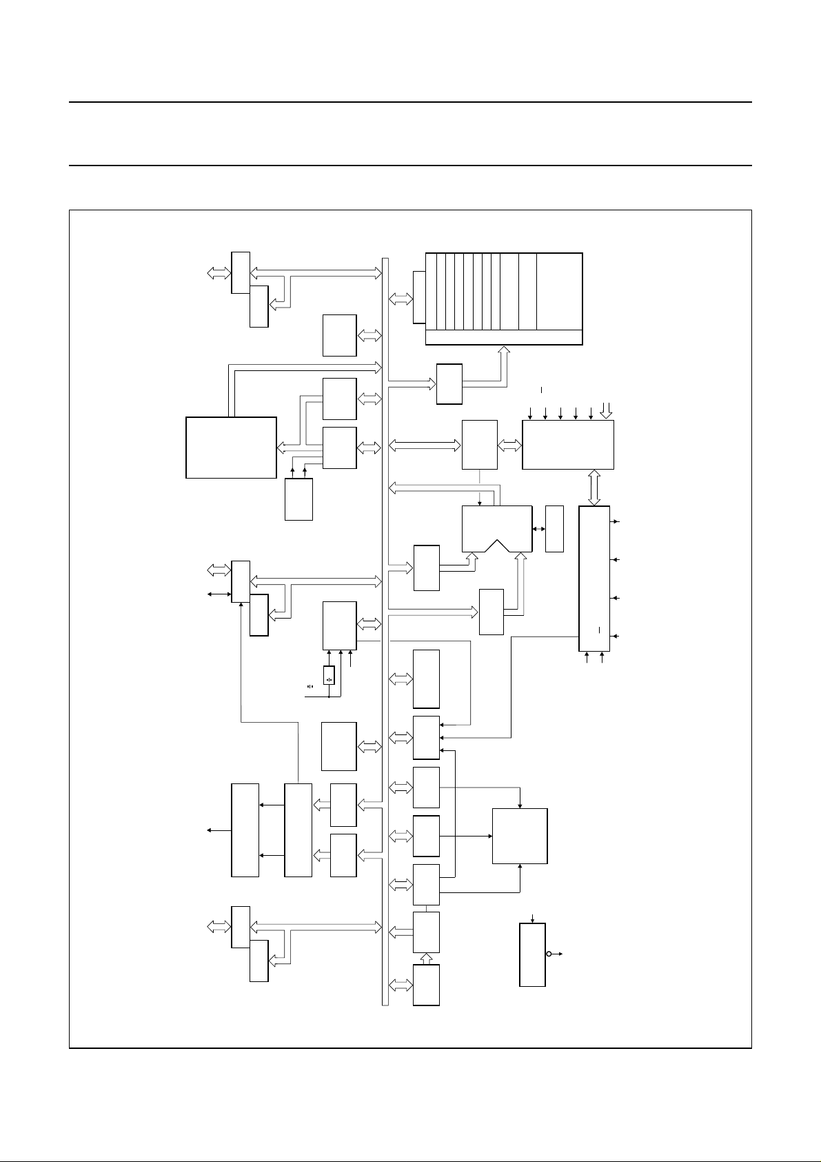
4 BLOCK DIAGRAM
8
PORT 0
P0.0 to P0.7
2 kbytes
RESIDENT ROM
P1.7/MDY P1.0 to P1.6
BUFFER
6 kbytes
4 kbytes
(PCD3353C; 53A)
(PCD3352C; 52A)
(PCD3351C; 51A)
PORT 1
BUFFER
PORT 0
FLIP-FLOP
PORT 1
FLIP-FLOP
DECODE
INTERNAL
BANK
MEMORY
FLIP-FLOPS
FREQ.
CLOCK
30
WORD
STATUS
PROGRAM
LOWER
COUNTER
PROGRAM
5888 8
HIGHER
COUNTER
PROGRAM
PCD3351A
PCD3352A
PCD3353A
PCA3351C
PCA3352C
PCA3353C
8
8
EVENT
TIMER/
COUNTER
32
T1
8
8
88
88
8
REGISTER 0
REGISTER 1
REGISTER 2
MULTIPLEXER
RAM
ADDRESS
REGISTER 1
TEMPORARY
ACCUMULATOR
REGISTER 3
REGISTER 4
REGISTER 5
REGISTER
REGISTER
INSTRUCTION
ARITHMETIC
timer interrupt
REGISTER 6
REGISTER 7
8 LEVEL STACK
DECOD
AND
DECODER
REGISTER 2
TEMPORARY
external interrupt
PCA3351C; 52C; 53C;
PCD3351A; 52A; 53A
MLA537
64 bytes
DATA STORE
REGISTER BANK
OPTIONAL SECOND
(VARIABLE LENGTH)
E
FLAG
T1
CE/T0
TIMER
CONDITIONAL
ADJUST
DECIMAL
LOGIC UNIT
BRANCH
128 bytes
(PCD3351C; 51A)
RESIDENT RAM ARRAY
TEST
ACC BIT
ACC
CARRY
LOGIC
XTAL2XTAL1RESET
CONTROL AND TIMING
CE/T0
IDLE
STOP
(PCD3352C; 52A; 53C; 53A)
OSCILLATOR
INTERRUPT INITIALIZE
handbook, full pagewidth
Fig.1 Block diagram.
This text is here in white to force landscape pages to be rotated correctly when browsing through the pdf in the Acrobat reader.This text is here in
_white to force landscape pages to be rotated correctly when browsing through the pdf in the Acrobat reader.This text is here inThis text is here in
white to force landscape pages to be rotated correctly when browsing through the pdf in the Acrobat reader. white to force landscape pages to be ...
1999 Oct 28 5
TONE
4 7
P2.0 to P2.3
FILTER
PORT 2
BUFFER
PORT 2
FLIP-FLOP
SINE WAVE
GENERATOR
MELODY
CONTROL
REGISTER
LGF
REGISTER
HGF
REGISTER
8
8
8
8
8
8
LOGIC
INTERRUPT
DATA
EEPROM
TRANSFER
EEPROM
ADDRESS
REGISTER
EEPROM
CONTROL
REGISTER
TIMER 2
REGISTER
TIMER 2
RELOAD
REGISTER
interrupt
derivative
EEPROM
POR
V
POWER-ON-RESET
RESET
8
8
8
4
Philips Semiconductors Product specification
8-bit microcontrollers with DTMF generator
and 128 bytes EEPROM
5 PINNING INFORMATION
5.1 Pinning
handbook, halfpage
(1) PCA335xC denotes:
PCA3351C, PCA3352C or
PCA3353C.
PCD335xA denotes:
PCD3351A, PCD3352A or
PCD3353A.
P0.1
P0.2
P0.3
P0.4
P0.5
P0.6
P0.7
T1
XTAL1
XTAL2
RESET
CE/T0
P1.0
P1.1
1
2
3
4
5
6
PCA335xC
7
PCD335xA
8
9
10
11
12
13
(1)
MLA538
28
27
26
25
24
23
22
21
20
19
18
17
16
1514
P0.0
P2.3
P2.2
P2.1
V
DD
TONE
V
SS
P2.0
P1.7/MDY
P1.6
P1.5
P1.4
P1.3
P1.2
PCA3351C; 52C; 53C;
PCD3351A; 52A; 53A
handbook, full pagewidth
(1) PCA335xCH denotes:
PCA3351CH, PCA3352CH or
PCA3353CH.
PCD335xAH denotes:
PCD3351AH, PCD3352AH or
PCD3353AH.
Fig.2 Pin configuration for DIP28 (SOT117-1) and SO28 (SOT136-1).
P2.2
P2.3
P0.0
n.c.
P0.1
P0.2
P0.3
P0.4
31
n.c.
P0.5
P0.6
P0.7
T1
XTAL1
XTAL2
RESET
32
1
2
3
4
5
6
7
8
9
CE/T0
30
PCA335xCH
PCD335xAH
11
10
P1.0
P1.1
29
(1)
12
P1.2
28
13
n.c.
27
14
P1.3
26
15
P1.4
25
16
P1.5
24
23
22
21
20
19
18
17
MGB795
P2.1
V
DD
TONE
V
SS
P2.0
P1.7/MDY
P1.6
n.c.
Fig.3 Pin configuration for LQFP32 (SOT358-1).
1999 Oct 28 6
Philips Semiconductors Product specification
8-bit microcontrollers with DTMF generator
and 128 bytes EEPROM
5.2 Pin description
Table 2 SOT117-1 and SOT136-1 packages (for information on parallel I/O ports, see Chapter 14)
SYMBOL PIN TYPE DESCRIPTION
P0.1 to P0.7 1 to 7 I/O 7 bits of Port 0: 8-bit quasi-bidirectional I/O port
T1 8 I Test 1 or count input of 8-bit Timer/event counter 1
XTAL1 9 I crystal oscillator or external clock input
XTAL2 10 O crystal oscillator output
RESET 11 I reset input
CE/
T0 12 I Chip Enable or Test 0
P1.0 to P1.6 13 to 19 I/O 7 bits of Port 1: 8-bit quasi-bidirectional I/O port
P1.7/MDY 20 I/O 1 bit of Port 1: 8-bit quasi-bidirectional I/O port; or melody output
P2.0 21 I/O 1 bit of Port 2: 4-bit quasi-bidirectional I/O port
V
SS
TONE 23 O DTMF output
V
DD
P2.1 to P2.3 25 to 27 I/O 3 bits of Port 2: 4-bit quasi-bidirectional I/O port
P0.0 28 I/O 1 bit of Port 0: 8-bit quasi-bidirectional I/O port
22 P ground
24 P positive supply voltage
PCA3351C; 52C; 53C;
PCD3351A; 52A; 53A
Table 3 SOT358-1 package (for information on parallel I/O ports, see Chapter 14)
SYMBOL PIN TYPE DESCRIPTION
n.c. 1 − not connected
P0.5 to P0.7 2 to 4 I/O 3 bits of Port 0: 8-bit quasi-bidirectional I/O port
T1 5 I Test 1 or count input of 8-bit Timer/event counter 1
XTAL1 6 I crystal oscillator or external clock input
XTAL2 7 O crystal oscillator output
RESET 8 I reset input
CE/
T0 9 I Chip Enable or Test 0
P1.0 to P1.2 10 to 12 I/O 3 bits of Port 1: 8-bit quasi-bidirectional I/O port
n.c. 13 − not connected
P1.3 to P1.5 14 to 16 I/O 3 bits of Port 1: 8-bit quasi-bidirectional I/O port
n.c. 17 − not connected
P1.6 18 I/O 1 bit of Port 1: 8-bit quasi-bidirectional I/O port
P1.7/MDY 19 I/O 1 bit of Port 1: 8-bit quasi-bidirectional I/O port; or melody output
P2.0 20 I/O 1 bit of Port 2: 4-bit quasi-bidirectional I/O port
V
SS
TONE 22 O DTMF output
V
DD
P2.1 to P2.3 24 to 26 I/O 3 bits of Port 2: 4-bit quasi-bidirectional I/O port
P0.0 27 I/O 1 bit of Port 0: 8-bit quasi-bidirectional I/O port
n.c. 28 − not connected
P0.1 to P0.4 29 to 32 I/O 4 bits of Port 0: 8-bit quasi-bidirectional I/O port
21 P ground
23 P positive supply voltage
1999 Oct 28 7

Philips Semiconductors Product specification
8-bit microcontrollers with DTMF generator
and 128 bytes EEPROM
6 FREQUENCY GENERATOR
A versatile frequency generator section is provided (see
Fig.4). For normal operation, use a 3.58 MHz quartz
crystal or PXE resonator. The frequency generator
includes precision circuitry for dual tone multifrequency
(DTMF) signals, which is typically used for tone dialling
telephone sets.
Theirfrequenciesareprovidedinpurely sinusoidal form on
the TONE output or as square waves on the port line
P1.7/MDY.
6.1 Frequency generator derivative registers
6.1.1 HIGH AND LOW GROUP FREQUENCY REGISTERS
Table 4 gives the addresses, symbols and access types of the High Group Frequency (HGF) and Low Group Frequency
(LGF) registers.
Table 4 Hexadecimal addresses, symbols, access types and bit symbols of the frequency registers
REGISTER
ADDRESS
11H HGF W H7H6H5H4H3H2H1H0
12H LGF W L7L6L5L4L3L2L1L0
REGISTER
SYMBOL
ACCESS
TYPE
7 6 5 4 3 2 1 0
The TONE output can alternatively issue twelve modem
frequencies for data rates between 300 and 1200 bits/s.
In addition to DTMF and modem frequencies, two octaves
of musical scale in steps of semitones are available.
When no tones are generated the TONE output is in
3-state mode.
BIT SYMBOLS
PCA3351C; 52C; 53C;
PCD3351A; 52A; 53A
6.1.2 MELODY CONTROL REGISTER (MDYCON)
Table 5 Melody Control Register, MDYCON (address 13H; access type R/W)
7 6 5 4 3 2 1 0
0000000EMO
Table 6 Description of MDYCON bits
BIT SYMBOL DESCRIPTION
7to1 − These bits are set to a logic 0.
0 EMO Enable Melody Output. If bit EMO = 0, then P1.7/MDY is a standard port line.
If bit EMO = 1, then P1.7/MDY is the melody output. EMO = 1 does not inhibit the port
instructions for P1.7/MDY. Therefore the state of both port line and flip-flop may be read
in and the port flip-flop may be written by port instructions. However, the port flip-flop of
P1.7/MDY must remain set to avoid conflicts between melody and port outputs.
When the HGF contents are zero while EMO = 1, P1.7/MDY is in the HIGH state.
1999 Oct 28 8
Philips Semiconductors Product specification
8-bit microcontrollers with DTMF generator
and 128 bytes EEPROM
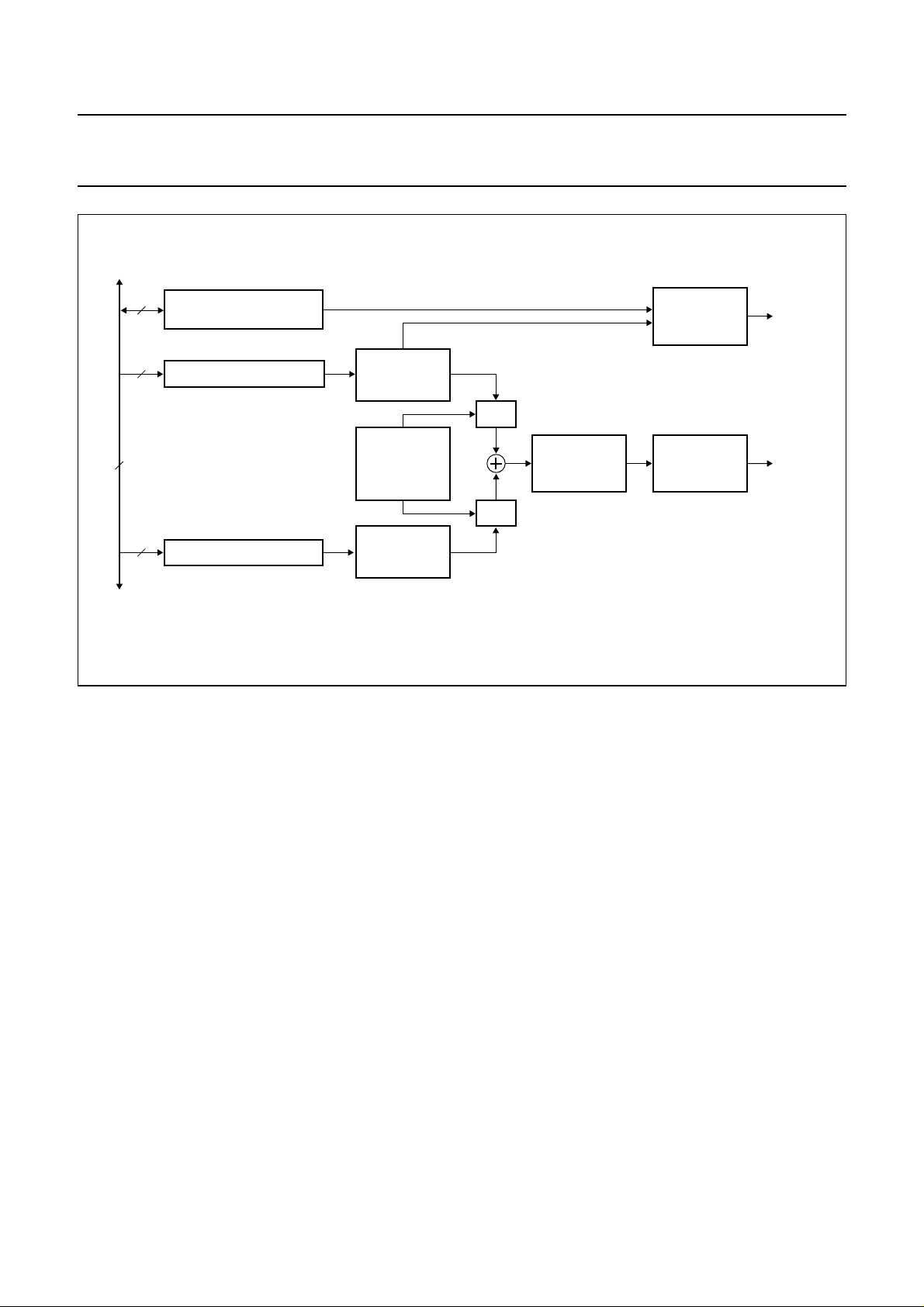
handbook, full pagewidth
8
8
8
INTERNAL BUS
8
MELODY CONTROL
REGISTER
HGF REGISTER
LGF REGISTER
DIGITAL
SINE WAVE
SYNTHESIZER
SWITCHED
CAPACITOR
BANDGAP
VOLTAGE
REFERENCE
DIGITAL
SINE WAVE
SYNTHESIZER
square wave
DAC
DAC
SWITCHED
CAPACITOR
LOW-PASS
FILTER
PCA3351C; 52C; 53C;
PCD3351A; 52A; 53A
PORT/MELODY
OUTPUT LOGIC
RC LOW-PASS
FILTER
MLC416
P1.7/
MDY
TONE
Fig.4 Block diagram of the frequency generator and melody output (P1.7/MDY) section.
1999 Oct 28 9

Philips Semiconductors Product specification
8-bit microcontrollers with DTMF generator
and 128 bytes EEPROM
6.2 Melody output (P1.7/MDY)
The melody output (P1.7/MDY) is very useful for
generating musical notes when a purely sinusoidal signal
is not required, such as for ringer applications.
The square wave (duty cycle =12⁄23 or 52%) will include
the attenuated harmonics of the base frequency, which is
defined by the contents of the HGF register (Table 4).
However, even higher frequency notes may be produced
since the low-pass filtering on the TONE output is not
applied to the P1.7/MDY output. This results in the
minimum decimal value x in the HGF register (see
equation in Section 6.3) being 2 for the P1.7/MDY output,
rather than 60 for the TONE output. A sinusoidal TONE
output is produced at the same time as the melody square
wave, but due to the filtering, the higher frequency sine
waves with x < 60 will not appear at the TONE output.
Since the melody output is shared with P1.7, the port
flip-flop of P1.7 has to be set HIGH before using the
melodyoutput.Thistoavoidconflictsbetween melody and
port outputs. The melody output drive depends on the
configuration of port P1.7/MDY, see Chapter 14, Table 26.
6.3 Frequency registers
PCA3351C; 52C; 53C;
PCD3351A; 52A; 53A
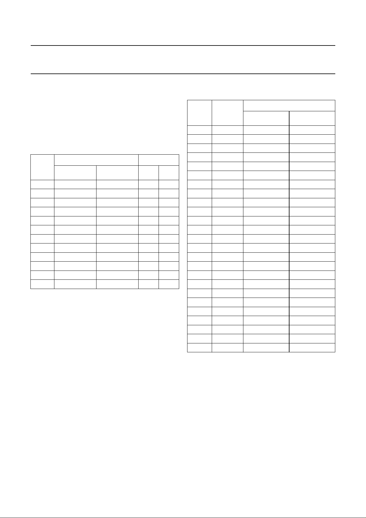
6.4 DTMF frequencies
Assuming an oscillator frequency f
DTMF standard frequencies can be implemented as
shown in Table 7.
The relationships between telephone keyboard symbols,
DTMFfrequencypairsandthefrequencyregistercontents
are given in Table 8.
Table 7 DTMF standard frequencies and their
implementation; value = LGF, HGF contents
VALUE
(HEX)
DD 697 697.90 0.13 0.90
C8 770 770.46 0.06 0.46
B5 852 850.45 −0.18 −1.55
A3 941 943.23 0.24 2.23
7F 1209 1206.45 −0.21 −2.55
72 1336 1341.66 0.42 5.66
67 1477 1482.21 0.35 5.21
5D 1633 1638.24 0.32 5.24
FREQUENCY (Hz) DEVIATION
STANDARD GENERATED (%) (Hz)
= 3.58 MHz, the
xtal
The two frequency registers HGF and LGF define two
frequencies. From these, the digital sine synthesizers
together with the Digital-to-Analog Converters (DACs)
construct two sine waves. Their amplitudes are precisely
scaled according to the bandgap voltage reference. This
ensures tone output levels independent of supply voltage
and temperature.
The amplitude of the Low Group Frequency sine wave is
attenuated by 2 dB compared to the amplitude of the High
Group Frequency sine wave.
The two sine waves are summed and then filtered by an
on-chip switched capacitor and RC low-pass filters. These
guarantee that all DTMF tones generated fulfil the CEPT
recommendations with respect to amplitude, frequency
deviation, total harmonic distortion and suppression of
unwanted frequency components.
The value 00H in a frequency register stops the
corresponding digital sine synthesizer. If both frequency
registers contain 00H, the whole frequency generator is
shut off, resulting in lower power consumption.
Thefrequencyofthesine wave generated from eitherHGF
or LGF is a function of the decimal value ‘x’ held in the
register. The variables are related by the equation:
f
xtal
f
=
----------------------------23 x 2+()[]
; where 60 ≤ x ≤ 255 for TONE output.
Table 8 Dialling symbols, corresponding DTMF
frequency pairs and frequency register contents
TELEPHONE
KEYBOARD
SYMBOLS
0 (941, 1336) A3 72
1 (697, 1209) DD 7F
2 (697, 1336) DD 72
3 (697, 1477) DD 67
4 (770, 1209) C8 7F
5 (770, 1336) C8 72
6 (770, 1477) C8 67
7 (852, 1209) B5 7F
8 (852, 1336) B5 72
9 (852, 1477) B5 67
A (697, 1633) DD 5D
B (770, 1633) C8 5D
C (852, 1633) B5 5D
D (941, 1633) A3 5D
• (941, 1209) A3 7F
# (941, 1477) A3 67
DTMF FREQ.
PAIRS
(Hz)
LGF
VALUE
(HEX)
HGF
VALUE
(HEX)
1999 Oct 28 10
Philips Semiconductors Product specification
8-bit microcontrollers with DTMF generator
and 128 bytes EEPROM
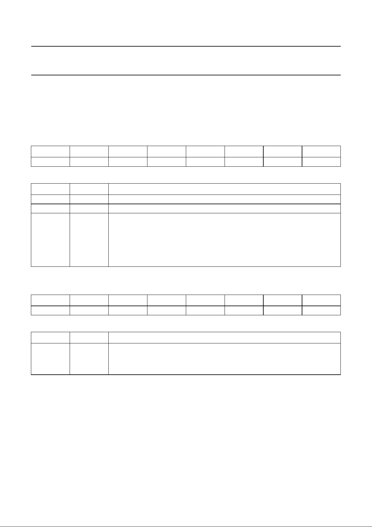
6.5 Modem frequencies
Again assuming an oscillator frequency f
the standard modem frequencies can be implemented as
in Table 9. It is suggested to define the frequency by the
HGF register while the LGF register contains 00H,
disabling Low Group Frequency generation.
Table 9 Standard modem frequencies and their
implementation
HGF
FREQUENCY (Hz) DEVIATION
VALUE
(HEX)
9D 980
82 1180
8F 1070
79 1270
80 1200
45 2200
76 1300
48 2100
5C 1650
52 1850
4B 2025
44 2225
MODEM GENERATED (%) (Hz)
(1)
(1)
(2)
(2)
(3)
(3)
(4)
(4)
(1)
(1)
(2)
(2)
978.82 −0.12 −1.18
1179.03 −0.08 −0.97
1073.33 0.31 3.33
1265.30 −0.37 −4.70
1197.17 −0.24 −2.83
2192.01 −0.36 −7.99
1296.94 −0.24 −3.06
2103.14 0.15 3.14
1655.66 0.34 5.66
1852.77 0.15 2.77
2021.20 −0.19 −3.80
2223.32 −0.08 −1.68
Notes
1. Standard is V.21.
2. Standard is Bell 103.
3. Standard is Bell 202.
4. Standard is V.23.
6.6 Musical scale frequencies
= 3.58 MHz,
xtal
PCA3351C; 52C; 53C;
PCD3351A; 52A; 53A
Table 10 Musical scale frequencies and their
implementation
HGF
NOTE
VALUE
(HEX)
D#5 F8 622.3 622.5
E5 EA 659.3 659.5
F5 DD 698.5 697.9
F#5 D0 740.0 741.1
G5 C5 784.0 782.1
G#5 B9 830.6 832.3
A5 AF 880.0 879.3
A#5 A5 923.3 931.9
B5 9C 987.8 985.0
C6 93 1046.5 1044.5
C#6 8A 1108.7 1111.7
D6 82 1174.7 1179.0
D#6 7B 1244.5 1245.1
E6 74 1318.5 1318.9
F6 6D 1396.9 1402.1
F#6 67 1480.0 1482.2
G6 61 1568.0 1572.0
G#6 5C 1661.2 1655.7
A6 56 1760.0 1768.5
A#6 51 1864.7 1875.1
B6 4D 1975.5 1970.0
C7 48 2093.0 2103.3
C#7 44 2217.5 2223.3
D7 40 2349.3 2358.1
D#7 3D 2489.0 2470.4
FREQUENCY (Hz)
STANDARD
(1)
GENERATED
Finally, two octaves of musical scale in steps of semitones
can be realized, again assuming an oscillator frequency
f
= 3.58 MHz (Table 10). It is suggested to define the
xtal
frequency by the HGF register while the LGF contains
00H, disabling Low Group Frequency generation
1999 Oct 28 11
Note
1. Standard scale based on A4 @ 440 Hz.

Philips Semiconductors Product specification
8-bit microcontrollers with DTMF generator
and 128 bytes EEPROM
7 EEPROM AND TIMER 2 ORGANIZATION
The PCD335xA and PCA335xC have 128 bytes of
Electrically Erasable Programmable Read-Only Memory
(EEPROM). Such non-volatile storage provides data
retention without the need for battery backup. In telecom
applications, the EEPROM is used for storing redial
numbersand for short dialling of frequently used numbers.
More generally, EEPROM may be used for customizing
microcontrollers, such as to include a PIN code or a
country code, to define trimming parameters, to select
application features from the range stored in ROM.
The most significant difference between a RAM and an
EEPROM is that a bit in EEPROM, once written to a
logic 1, cannot be cleared by a subsequent write
operation. Successive write accesses actually perform a
logical OR with the previously stored information.
Therefore, to clear a bit, the whole byte must be erased
and re-written with the particular bit cleared. Thus, an
erase-and-write operation is the EEPROM equivalent of a
RAM write operation
PCA3351C; 52C; 53C;
PCD3351A; 52A; 53A
Whereas read access times to an EEPROM are
comparable to RAM access times, write and erase access
times are much slower at 5 ms each. To make these
operations more efficient, several provisions are available
in the PCD335xA and PCA335xC.
First, the EEPROM array is structured into 32 four-byte
pages (see Fig.5) permitting access to 4 bytes in parallel
(write page, erase/write page and erase page). It is also
possible to erase and write individual bytes. Finally, the
EEPROM address register provides auto-incrementing,
allowing very efficient read and write accesses to
sequential bytes.
To simplify the erase and write timing, the derivative 8-bit
down-counter (Timer 2) with reload register is provided.
In addition to EEPROM timing, Timer 2 can be used for
general real-time tasks, such as for measuring signal
duration and for defining pulse widths.
1999 Oct 28 12

Philips Semiconductors Product specification
8-bit microcontrollers with DTMF generator
and 128 bytes EEPROM
handbook, full pagewidth
8
EEPROM ADDRESS REGISTER
2
2 : 4 DECODER
EEPROM LATCH 0
8
F0
F1EEPROM LATCH 1
F2EEPROM LATCH 2
F3EEPROM LATCH 3
PCA3351C; 52C; 53C;
PCD3351A; 52A; 53A
5
5 : 32 DECODER
128-byte EEPROM ARRAY
(32 4-byte PAGES)
8
INTERNAL
BUS
8
8
8
8
8
EEPROM TEST REGISTER
EEPROM CONTROL REGISTER
TIMER 2 RELOAD REGISTER
8
TIMER 2 REGISTER (T2)
1
f
xtal
480
MGB824
T2F set on
underflow
Fig.5 Block diagram of the EEPROM and Timer 2.
1999 Oct 28 13

Philips Semiconductors Product specification
8-bit microcontrollers with DTMF generator
and 128 bytes EEPROM
7.1 EEPROM registers
7.1.1 EEPROM CONTROL REGISTER (EPCR)
The behaviour of the EEPROM and Timer 2 section is defined by the EEPROM Control Register. See Tables 11, 12 and
13.
Table 11 EEPROM Control Register, EPCR (address 04H, access type R/W)
76543210
STT2 ET2I T2F EWP MC3 MC2 MC1 0
Table 12 Description of the EPCR bits
BIT SYMBOL DESCRIPTION
7 STT2 Start T2. If STT2 = 0, then Timer 2 is stopped; T2 value held. If STT2 = 1, then T2
decrements from reload value.
6 ET2I Enable T2 interrupt. If ET2I = 0, then T2F event cannot request interrupt. If ET2I = 1,
then T2F event can request interrupt.
5 T2F Timer 2 flag. Set when T2 underflows (or by program); reset by program.
4 EWP Erase or write in progress (EWP). Set by program (EWP starts EEPROM erase and/or
write and Timer 2). Reset at the end of EEPROM erase and/or write.
3 MC3 Mode control 3 to 1. These three bits in conjunction with bit EWP select the mode as
2 MC2
1 MC1
0 − This bit is set to a logic 0.
shown in Table 13.
PCA3351C; 52C; 53C;
PCD3351A; 52A; 53A
Table 13 Mode selection; X = don’t care
EWP MC3 MC2 MC1 DESCRIPTION
0000read byte
0010increment mode
1 0 1 X write page
1100erase/write page
1111erase page
X 0 0 1 not allowed
X101
X110
1999 Oct 28 14
Philips Semiconductors Product specification
8-bit microcontrollers with DTMF generator
and 128 bytes EEPROM
7.1.2 EEPROM ADDRESS REGISTER (ADDR)
The EEPROM Address Register determines the EEPROM location to which an EEPROM access is directed.
As a whole, ADDR auto-increments after read and write cycles to EEPROM, but remains fixed after erase cycles. This
behaviour generates the correct ADDR contents for sequential read accesses and for sequential write or erase/write
accesses with intermediate page setup. Overflow of the 8-bit counter wraps around to zero.
Table 14 EEPROM Address Register, ADDR (address 01H, access type R/W)
76543210
0 AD6 AD5 AD4 AD3 AD2 AD1 AD0
Table 15 Description of ADDR bits
BIT SYMBOL DESCRIPTION
7 − This bit is set to a logic 0.
6 to 2 AD6 to AD2 AD2 to AD6 select one of 32 pages.
1 to 0 AD1 to AD0 AD1 and AD0 are irrelevant during erase and write cycles. For read accesses, AD0 and
AD1 indicate the byte location within an EEPROM page. During page setup, finally, AD0
and AD1 select EEPROM Latch 0 to 3 whereas AD2 to AD6 are irrelevant. If increment
mode (Table 13) is active during page setup, the subcounter consisting of AD0 and AD1
increments after every write to an EEPROM latch, thus enhancing access to sequential
EEPROM latches. Incrementing stops when EEPROM Latch 3 is reached, i.e. when
AD0 and AD1 are both a logic 1.
PCA3351C; 52C; 53C;
PCD3351A; 52A; 53A
7.1.3 EEPROM DATA REGISTER (DATR)
Table 16 EEPROM Data Register, DATR (address 03H; access type R/W)
76543210
D7 D6 D5 D4 D3 D2 D1 D0
Table 17 Description of DATR bits
BIT SYMBOL DESCRIPTION
7 to 0 D7 to D0 The EEPROM Data Register (DATR) is only a conceptual entity. A read operation from
DATR, reads out the EEPROM byte addressed by ADDR. On the other hand, a write
operation to DATR, loads data into the EEPROM latch (see Fig.5) defined by bits AD0
and AD1 of ADDR.
7.1.4 EEPROM TEST REGISTER (TST)
The EEPROM Test register is used for testing purposes during device manufacture. It must not be accessed by the
device user.
1999 Oct 28 15

Philips Semiconductors Product specification
8-bit microcontrollers with DTMF generator
and 128 bytes EEPROM
7.2 EEPROM latches
The four EEPROM latches (EEPROM Latch 0 to 3; Fig.5)
cannotberead by user software. Due to their construction,
thelatchescanonlybepreset,but not cleared. Successive
write operations through DATR to the EEPROM latches
actually perform a logical OR with the previously stored
data in EEPROM. The EEPROM latches are reset at the
conclusion of any EEPROM cycle.
7.3 EEPROM flags
The four EEPROM flags (F0 to F3; Fig.5) cannot be
directly accessed by user software. An EEPROM flag is
set as a side-effect when the corresponding EEPROM
latch is written through DATR. The EEPROM flags are
reset at the conclusion of any EEPROM cycle.
7.4 EEPROM macros
The instruction sequence used in an EEPROM access
should be treated as an indivisible entity. Erroneous
programs result if ADDR, DATR, RELR or EPCR are
inadvertently changed during an EEPROM cycle or its
setup. Special care should be taken if the program may
asynchronouslydivert due to an interrupt. A new accessto
theEEPROMmayonlybeinitiatedwhennowrite,eraseor
erase/write cycles are in progress. This can be verified by
reading bit EWP (register EPCR).
For write, erase and erase/write cycles, it is assumed that
theTimer 2 Reload Register (RELR) has been loaded with
the appropriate value for a 5 ms delay, which depends on
f
(seeTable 24).Theendofawrite,eraseorerase/write
xtal
cycle will be signalled by a cleared EWP and by a Timer 2
interrupt provided that ET2I = 1 and that the derivative
interrupt is enabled.
7.5 EEPROM access
One read, one write, one erase/write and one erase
access are defined by bits EWP and MC1 to MC3 in the
EPCR register; see Table 11.
Read byte retrieves the EEPROM byte addressed by
ADDR when DATR is read. Read cycles are
instantaneous.
Write and erase cycles take 5 ms, however. Erase/write is
a combination of an erase and a subsequent write cycle,
consequently taking 10 ms.
PCA3351C; 52C; 53C;
PCD3351A; 52A; 53A
However, write and erase cycles need not affect all bytes
of the page. The EEPROM flags F0 to F3 (see Fig.5)
determine which bytes within the EEPROM page are
affected by the erase and/or write cycles. A byte whose
corresponding EEPROM flag is zero remains unchanged.
With erase page, a byte is erased if its corresponding
EEPROM flag is set. With write page, data in EEPROM
Latch 0 to 3 (Fig.5) are ORed to the individual page bytes
if and only if the corresponding EEPROM flags are set.
In an erase/write cycle, F0 to F3 select which page bytes
are erased and ORed with the corresponding EEPROM
latches.
ORing, in this event, means that the EEPROM latches are
copied to the selected page bytes.
The described page-wise organization of erase and write
cycles allows up to four bytes to be individually erased or
written within 5 ms. This advantage necessitates a
preparation step, called page setup, before the actual
erase and/or write cycle can be executed.
Page setup controls EEPROM latches and EEPROM
flags. This will be described in the Sections 7.5.1 to 7.5.5.
7.5.1 PAGE SETUP
Page setup is a preparation step required before write
page, erase page and erase/write page cycles.
As previously described, these page operations include
single-bytewrite,eraseanderase/writeasaspecialevent.
EEPROM flags F0 to F3 determine which page bytes will
be affected by the mentioned page operations. EEPROM
Latch 0 to 3 must be preset through DATR to specify the
write cycle data to EEPROM and to setthe EEPROM flags
as a side-effect. Obviously, the actual preset value of the
EEPROM latches is irrelevant for erase page. Preset of
one, two, three or all four EEPROM latches and the
corresponding EEPROM flags can be performed by
repeatedly defining ADDR and writing to DATR (see
Table 18).
If more than one EEPROM latch must be preset, the
subcounter consisting of AD0 and AD1 can be induced to
auto-increment after every write to DATR, thus stepping
through all EEPROM latches. For this purpose, increment
mode (Table 13) must be selected. Auto-incrementing
stops at EEPROM Latch 3. It is not mandatory to start at
EEPROM Latch 0 as in shown in Table 19.
As their names imply, write page, erase page and
erase/write page are applied to a whole EEPROM page.
Therefore, bits AD0 and AD1 of register ADDR (see
Table 14), defining the byte location within an EEPROM
page, are irrelevant during write and erase cycles.
1999 Oct 28 16
Note that AD2 to AD6 are irrelevant during page setup.
They will usually specify the intended EEPROM page,
anticipating the subsequent page cycle.

Philips Semiconductors Product specification
8-bit microcontrollers with DTMF generator
and 128 bytes EEPROM
From now on, it will be assumed that AD2 to AD6 will
contain the intended EEPROM page address after page
setup.
Table 18 Page setup; preset
INSTRUCTION RESULT
MOVA, #addr address of EEPROM latch
MOVADDR, A send address to ADDR
MOVA, #data load write, erase/write or erase data
MOV DATR, A send data to addressed EEPROM
latch
Table 19 Page setup; auto-incrementing
INSTRUCTION RESULT
MOVA, #MC2 increment mode control word
MOV EPCR, A select increment mode
MOVA, #baddr EEPROM Latch 0 address
(AD0 = AD1 = 0)
MOVADDR, A send EEPROM Latch 0 address to
ADDR
MOVA, R0 load 1stbyte from Register 0
MOV DATR, A send 1
MOVA, R1 load 2
MOV DATR, A send 2
MOVA, R2 load 3
MOV DATR, A send 3
MOVA, R3 load 4
MOV DATR, A send 4
st
byte to EEPROM Latch 0
nd
byte from Register 1
nd
byte to EEPROM Latch 1
rd
byte from Register 2
rd
byte to EEPROM Latch 2
th
byte from Register 3
th
byte to EEPROM Latch 3
PCA3351C; 52C; 53C;
PCD3351A; 52A; 53A
latches, the corresponding bytes in the page should
previously have been erased.
The EEPROM latches are preset as described in
Section 7.5.1. The actual transfer to the EEPROM is then
performed as shown in Table 21.
The last instruction also starts Timer 2. The data in the
EEPROM latches are ORed with that in the corresponding
page bytes within 5 ms. A single-byte write is simply a
special case of ‘write page’.
ADDR auto-increments after the write cycle. If AD0 and
AD1 addressed EEPROM Latch 3 prior to the write cycle,
ADDR will point to the next EEPROM page (by bits AD2
to AD6) and to EEPROM Latch 0 (by bits AD0 and AD1).
This allows efficient coding of multi-page write operations.
Table 21 Write page
INSTRUCTION RESULT
MOVA, #EWP + MC2 ‘write page’ control word
MOV EPCR, A start ‘write page’ cycle
7.5.4 ERASE/WRITE PAGE
The EEPROM latches are preset as described in
Section 7.5.1. The page bytes corresponding to the
asserted flags (among F0 to F3) are erased and re-written
with the contents of the respective EEPROM latches.
The last instruction also starts Timer 2. Erasure takes
5 ms upon which Timer Register T2 reloads for another
5 ms cycle for writing. The top cycles together take 10 ms.
A single-byte erase/write is simply a special case of
‘erase/write page’.
7.5.2 READ BYTE
SinceADDRauto-incrementsaftera read cycle regardless
of the page boundary, successive bytes can efficiently be
read by repeating the last instruction.
Table 20 Read byte
INSTRUCTION RESULT
MOVA, #RDADDR load read address
MOVADDR, A send address to ADDR
MOVA, DATR read EEPROM data
7.5.3 W
The write cycle performs a logical OR between the data in
the EEPROM latches and that in the addressed EEPROM
page. To actually copy the data from the EEPROM
1999 Oct 28 17
RITE PAGE
ADDR auto-increments after the write cycle. If AD0 and
AD1 addressed EEPROM Latch 3 prior to the write cycle,
ADDR will point to the next EEPROM page (by AD2 to
AD6) and to EEPROM Latch 0 (by AD0 and AD1). This
allows efficient coding of multi-page erase/write
operations.
Table 22 Erase/write page
INSTRUCTION RESULT
MOVA, #EWP + MC3 ‘erase/write page’ control word
MOV EPCR, A start ‘erase/write page’ cycle
Philips Semiconductors Product specification
8-bit microcontrollers with DTMF generator
and 128 bytes EEPROM
7.5.5 ERASE PAGE
The EEPROM flags are set as described in Section 7.5.1.
The corresponding page bytes are erased.
The last instruction also starts Timer 2. Erasure takes
5 ms.Asingle-byteeraseissimplyaspecialcaseof‘erase
page’.
Note that ADDR does not auto-increment after an erase
cycle.
Table 23 Erase page
INSTRUCTION RESULT
MOVA, #EWP + MC3 + MC2 + MC1 ‘erase page’
control word
MOV EPCR, A start ‘erase
page’ cycle
7.6 Timer 2
Timer 2 is a 8-bit down-counter decremented at a rate of
1
⁄
× f
480
a general purpose timer. Conflicts between the two
applications should be carefully avoided.
7.6.1 T
When used for EEPROM timing, Timer 2 serves to
generate the 5 ms intervals needed for erasing or writing
the EEPROM. At the decrement rate of
reload value for a 5 ms interval is a function of f
Table 24 summarizes the required reload values for a
number of oscillator frequencies.
. It may be used either for EEPROM timing or as
xtal
IMER 2 FOR EEPROM TIMING
1
⁄
× f
xtal
xtal
, the
480
.
PCA3351C; 52C; 53C;
PCD3351A; 52A; 53A
The second underflow of an erase/write cycle and the first
underflow of write page and erase page conclude the
corresponding EEPROM cycle. Timer 2 is stopped, T2F is
set whereas EWP and MC1 to MC3 are cleared.
Table 24 Reload values as a function of f
f
xtal
(MHz)
RELOAD VALUE
(HEX)
10A
214
3.58 25
63E
10 68
16 A6
Note
1. The reload value is (5 × 10−3×1⁄
f
in MHz.
xtal
7.6.2 TIMER 2 AS A GENERAL PURPOSE TIMER
When used for purposes other than EEPROM timing,
Timer 2 is started by setting STT2. The Timer Register T2
(see Table 27) is loaded with the reload value from RELR.
T2 decrements to zero. On underflow, T2 is reloaded from
RELR, T2F is set and T2 continues to decrement.
Timer 2 can be stopped at any time by clearing STT2.
The value of T2 is then held and can be read out. After
setting STT2 again, Timer 2 decrements from the reload
value. Alternatively, it is possible to read T2 ‘on the fly’ i.e.
while Timer 2 is operating.
480
× f
xtal
(1)
xtal
) − 1;
Timer 2 is started by setting bit EWP in the EPCR.
TheTimerRegister T2isloadedwiththereloadvaluefrom
RELR. T2 decrements to zero.
Foran erase/write cycle, underflow of T2 indicates theend
of the erase operation. Therefore, Timer Register T2 is
reloaded from RELR for another 5 ms interval during
which the flagged EEPROM latches are copied to the
corresponding bytes in the page addressed by ADDR.
1999 Oct 28 18

Philips Semiconductors Product specification
8-bit microcontrollers with DTMF generator
and 128 bytes EEPROM
8 DERIVATIVE INTERRUPTS
One derivative interrupt event is defined. It is controlled by
bits T2F and ET2I in the EPCR (see Tables 11 and 12).
Thederivativeinterrupt event occurs when T2F is set. This
request is honoured under the following circumstances:
• No interrupt routine proceeds
• No external interrupt request is pending
• The derivative interrupt is enabled
• ET2I is set.
The derivative interrupt routine must include instructions
that will remove the cause of the derivative interrupt by
explicitly clearing T2F. If the derivative interrupt is not
used, T2F may directly be tested by the program.
Obviously, T2F can also be asserted under program
control, e.g. to generate a software interrupt.
9 TIMING
Although the PCD335xA and PCA335xC operate over a
clock frequency range from 1 to 16 MHz, f
will usually be chosen to take full advantage of the
frequency generator section.
10 RESET
In addition to the conditions given in the
Family”
the reset state.
data sheet, all derivative registers are cleared in
= 3.58 MHz
xtal
“PCD33XXA
PCA3351C; 52C; 53C;
PCD3351A; 52A; 53A
After exit from Stop mode by a HIGH level on CE/T0,
Timer 2 proceeds from the held state.
13 INSTRUCTION SET RESTRICTIONS
• For PCD3351A and PCA3351C only:
– ROM space being restricted to 2 kbytes, the
‘SEL MB1/2/3’ instructions would define non-existing
program memory banks and should therefore be
avoided.
– RAM space being restricted to 64 bytes, care should
be taken to avoid accesses to non-existing RAM
locations.
• For PCD3352A and PCA3352C only:
– ROM space being restricted to 4 kbytes, the
‘SEL MB2/3’ instructions would define non-existing
program memory banks and should therefore be
avoided.
• For PCD3353A and PCA3353Conly:
– ROM space being restricted to 6 kbytes, the
‘SEL MB3’ instructions would define non-existing
program memory banks and should therefore be
avoided.
• For the PCD3352A, PCD3353A, PCA3352C and
PCA3353C, RAM space is restricted to 128 bytes, thus
care should be taken to avoid accesses to non-existing
RAM locations.
11 IDLE MODE
In Idle mode, the frequency generator, the EEPROM and
the Timer 2 sections remain operative. Therefore, the
IDLE instruction may be executed while an erase and/or
write access to EEPROM is in progress.
12 STOP MODE
Since the oscillator is switched off, the frequency
generator, the EEPROM and the Timer 2 sections receive
no clock. It is suggested to clear both the HGF and the
LGF registers before entering Stop mode. This will cut off
the biasing of the internal amplifiers, considerably
reducing current requirements.
The Stop mode must not be entered while an erase
and/or write access to EEPROM is in progress. The STOP
instruction may only be executed when EWP in EPCR is
zero. The Timer 2 section is frozen during Stop mode.
1999 Oct 28 19
Philips Semiconductors Product specification
8-bit microcontrollers with DTMF generator
PCA3351C; 52C; 53C;
and 128 bytes EEPROM
14 OVERVIEW OF PORT AND POWER-ON-RESET
CONFIGURATIONS
• The PCA335xC microcontrollers support one port and
Power-on-reset configuration which is compatible with
the OTP PCD3755E.
• The PCD335xA microcontrollers support two port and
Power-on-reset configurations which can be chosen:
one is compatible with the OTP PCD3755A, the other is
compatible with the OTP PCD3755E.
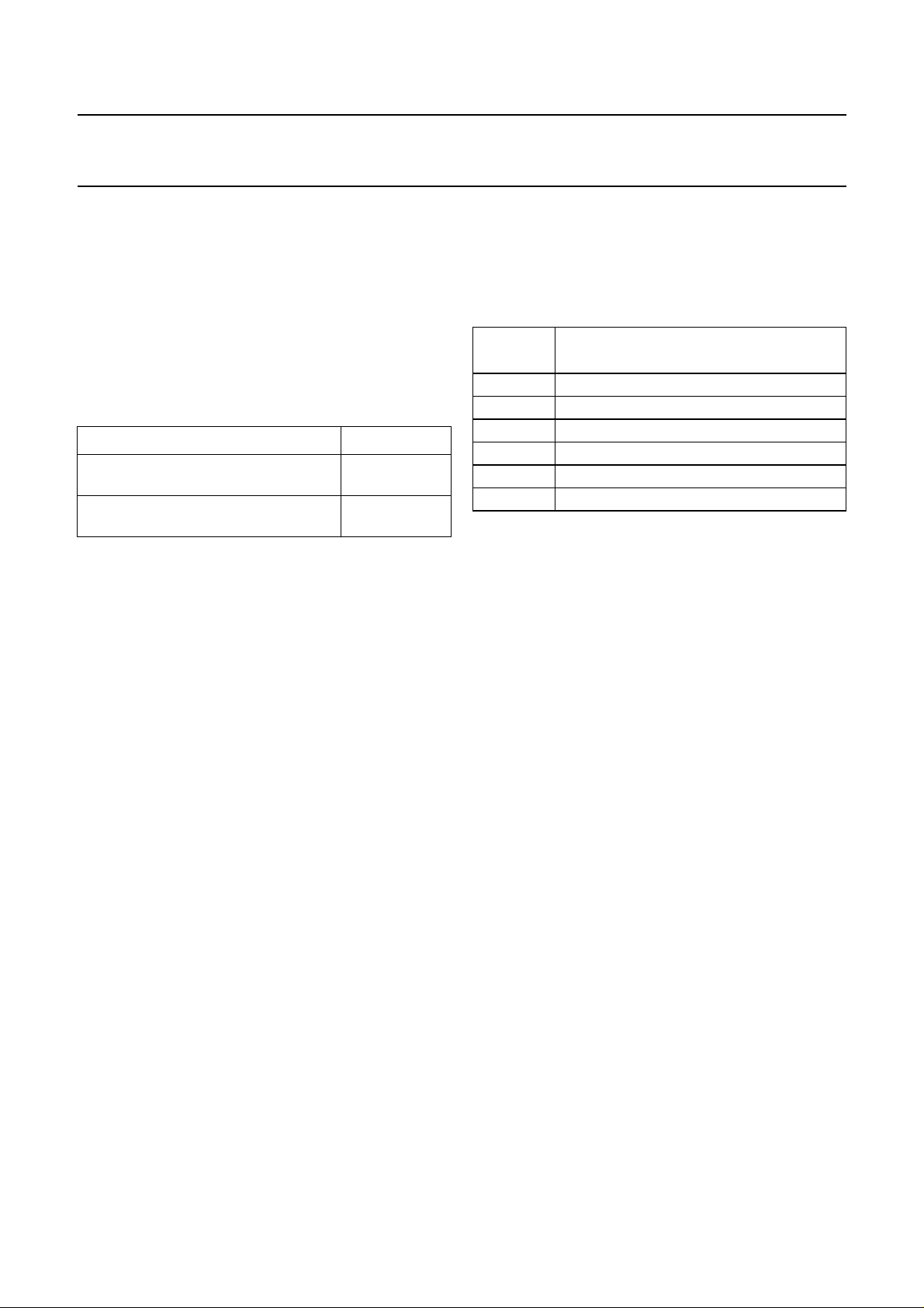
Table 26 Port and Power-on-Reset configurations
See note 1 and 2.
COVERED
BY OTP
PCD3755A 1S 1S 1S 1S 1S 1S 1S 1S 1S 1S 1S 1S 1S 1S 1R 1R
PCD3755E 1S 1S 1S 1S 1S 1S 1S 1S 2S 2S 2S 2S 2S 2S 1S 1S
012345670123456 7 0123
PORT 0 PORT 1 PORT 2
Table 25 Available mask configurations
TYPE
PCD3755A PCD3755E
PCA3351C − X
PCA3352C − X
PCA3353C − X
PCD3351A X X
PCD3352A X X
PCD3353A X X
PCD3351A; 52A; 53A
CONFIGURATION
V
POR
(3)
2S 2S 2S 2S 1.3 V
(3)
2S 1R 1R 1R 2.0 V
Notes
1. Port output drive: 1 = standard I/O; 2 = open-drain I/O, see
2. Port state after reset: S = Set (HIGH) and R = Reset (LOW).
3. The melody output drive type is push-pull.
“PCD33xxA Family”
data sheet.
1999 Oct 28 20
Philips Semiconductors Product specification
8-bit microcontrollers with DTMF generator
and 128 bytes EEPROM
15 SUMMARY OF DERIVATIVE REGISTERS
Table 27 Register map
ADDR.
(HEX)
00 not used
01 EEPROM Address Register
(ADDR)
02 not used
03 EEPROM Data Register
(DATR)
04 EEPROM Control Register
(EPCR)
05 Timer 2 Reload Register
(RELR)
06 Timer 2 Register
(T2)
07 Test Register
(TST)
08 to 10 not used
11 High Group Frequency Register
(HGF)
12 Low Group Frequency Register
(LGF)
13 Melody Control Register
(MDYCON)
14 to FF not used
REGISTER 7 6 5 43210R/W
0 AD6 AD5 AD4 AD3 AD2 AD1 AD0 R/W
D7 D6 D5 D4 D3 D2 D1 D0 R/W
STT2 ET21 TF2 EWP MC3 MC2 MC1 0 R/W
R7 R6 R5 R4 R3 R2 R1 R0 R/W
T2.7 T2.6 T2.5 T2.4 T2.3 T2.2 T2.1 T2.0 R
only for test purposes; not to be accessed by the device user
H7 H6 H5 H4 H3 H2 H1 H0 W
L7 L6 L5 L4 L3 L2 L1 L0 W
0000000EMOR/W
PCA3351C; 52C; 53C;
PCD3351A; 52A; 53A
16 HANDLING
Inputs and outputs are protected against electrostatic discharge in normal handling. However, it is good practice to take
normal precautions appropriate to handling MOS devices (see
“Data Handbook IC14, Section: Handling MOS devices”
17 LIMITING VALUES
In accordance with the Absolute Maximum Rating System (IEC 134).
SYMBOL PARAMETER MIN. MAX. UNIT
V
DD
V
I
I
I
I
O
P
tot
P
O
I
SS
T
stg
T
j
supply voltage −0.8 +7.0 V
all input voltages −0.5 VDD+ 0.5 V
DC input current −10 +10 mA
DC output current −10 +10 mA
total power dissipation − 125 mW
power dissipation per output − 30 mW
ground supply current −50 +50 mA
storage temperature −65 +150 °C
operating junction temperature − 90 °C
1999 Oct 28 21
).

Philips Semiconductors Product specification
8-bit microcontrollers with DTMF generator
and 128 bytes EEPROM
PCA3351C; 52C; 53C;
PCD3351A; 52A; 53A
18 DC CHARACTERISTICS
VDD= 1.8 to 6 V; VSS=0V;T
VSS; f
= 3.58 MHz; unless otherwise specified.
xtal
= 0 to +50 °C (PCA335xC) or −25 to +70 °C (PCD335xA); all voltages with respect to
amb
SYMBOL PARAMETER CONDITIONS MIN. TYP. MAX. UNIT
Supply
V
DD
supply voltage see Fig.6
operating note 1 1.8 − 6V
RAM data retention in Stop
1.0 − 6V
mode
I
DD
I
DD(idle)
I
DD(stp)
operating supply current see Figs 7 and 8; note 2
V
= 3 V; value HGFor LGF ≠ 0 − 0.8 1.6 mA
DD
V
=3V − 0.35 0.7 mA
DD
V
V
DD
DD
= 5 V; f
= 5 V; f
= 10 MHz − 1.5 4.0 mA
xtal
= 16 MHz − 2.4 6.0 mA
xtal
supply current (Idle mode) see Figs 9 and 10; note 2
V
= 3 V; value HGF or LGF ≠ 0 − 0.7 1.4 mA
DD
V
=3V − 0.25 0.5 mA
DD
V
V
DD
DD
= 5 V; f
= 5 V; f
= 10 MHz − 1.1 3.4 mA
xtal
= 16 MHz − 1.7 5.0 mA
xtal
supply current (Stop mode) see Fig.11; note 3
V
DD
V
DD
= 1.8 V; T
= 1.8 V; T
=25°C; − 1.0 5.5 µA
amb
=70°C; −−10 µA
amb
Inputs
V
IL
V
IH
I
LI
LOW level input voltage 0 − 0.3VDDV
HIGH level input voltage 0.7VDD− V
input leakage current VSS≤ VI≤ V
DD
−1 − 1 µA
DD
V
Port outputs
I
OL
I
OH
I
OH1
LOW level port sink current VDD= 3 V; VO= 0.4 V; see Fig.12 0.7 3.5 − mA
HIGH level pull-up output
source current
HIGH level push-pull output
VDD=3V; VO= 2.7 V; see Fig.13 −10 −30 −µA
V
=3V; VO= 0 V; see Fig.13 −−140 −300 µA
DD
VDD= 3 V; VO= 2.6 V; see Fig.14 −0.7 −3.5 − mA
source current
Tone output (see Fig.15)
V
HG(RMS)
V
LG(RMS)
f∆ f⁄
V
DC
output impedance − 100 500 Ω
Z
o
G
v
THD total harmonic distortion T
HGF voltage (RMS value) 158 181 205 mV
LGF voltage (RMS value) 125 142 160 mV
frequency deviation −0.6 − 0.6 %
DC voltage level − 0.5VDD− V
pre-emphasis of group 1.5 2.0 2.5 dB
=25°C; note 5 − 25 − dB
amb
1999 Oct 28 22

Philips Semiconductors Product specification
8-bit microcontrollers with DTMF generator
and 128 bytes EEPROM
PCA3351C; 52C; 53C;
PCD3351A; 52A; 53A
SYMBOL PARAMETER CONDITIONS MIN. TYP. MAX. UNIT
EEPROM (notes 1 and 6)
CY
t/w
endurance (erase/write
note 7 10
5
−−
cycles)
t
ret
data retention time 10 −−years
Power-on-reset (see Fig.16)
V
POR
Power-on-reset level
PCD335xA configuration as PCD3755A 0.8 1.3 1.8 V
PCD335xA configuration as PCD3755E 1.5 2.0 2.5 V
PCA335xC configuration as PCD3755E 1.7
(8)
2.0 2.3 V
Oscillator (see Fig.17)
g
m
R
F
transconductance VDD= 5 V 0.2 0.4 1.0 mS
feedback resistor 0.3 1.0 3.0 MΩ
Notes
1. TONE output, EEPROM erase and write require VDD≥ 2.5 V.
2. VIL=VSS; VIH=VDD; open-drain outputs connected to VSS; all other outputs open; value HGF = LGF = 0, unless
otherwise specified.
a) Maximum values: external clock at XTAL1 and XTAL2 open-circuit.
b) Typical values: T
=25°C; crystal connected between XTAL1 and XTAL2.
amb
3. VIL=VSS; VIH=VDD; RESET, T1 and CE/T0 at VSS; crystal connected between XTAL1 and XTAL2; pins T1 and
CE/T0 at VSS.
4. Values are specified for DTMF frequencies only (CEPT).
5. Related to the Low Group Frequency (LGF) component (CEPT).
6. After final testing the value of each EEPROM bit is a logic 1, but this cannot be guaranteed after board assembly.
7. Verified on sampling basis.
8. Each device is tested on the condition: V
DD(min)<VPOR
; to ensure a correct start-up, even for slow rising supply
voltages.
1999 Oct 28 23
Philips Semiconductors Product specification
8-bit microcontrollers with DTMF generator
and 128 bytes EEPROM
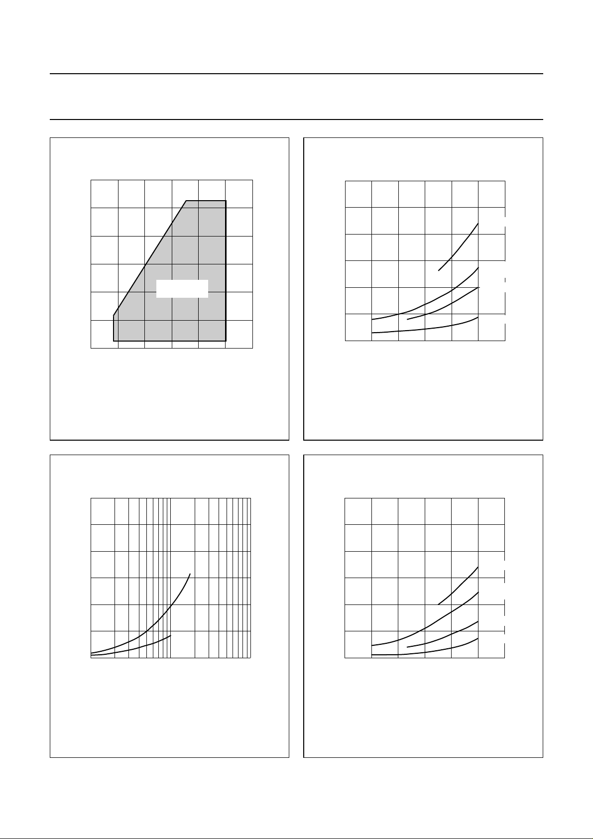
18
handbook, halfpage
f
xtal
(MHz)
15
12
9
6
3
0
135 7
guaranteed
operating range
MLA493
VDD (V)
I
DD
(mA)
6
4
2
0
1
handbook, halfpage
PCA3351C; 52C; 53C;
PCD3351A; 52A; 53A
MGB827
16 MHz
3.58 MHz
HGF or LGF ≠ 0
10 MHz
3.58 MHz
35
V
DD
(V)
7
Fig.6 Maximum clock frequency (f
function of supply voltage (VDD).
I
DD
(mA)
6
4
5 V
2
3 V
0
1
10 10
handbook, halfpage
f
xtal
xtal
(MHz)
) as a
MGB828
Measured with crystal between XTAL1 and XTAL2.
Fig.7 Typical operating supply current (IDD) as a
function of supply voltage (VDD).
MGB829
16 MHz
3.58 MHz
HGF or LGF ≠ 0
10 MHz
3.58 MHz
(V)
7
V
DD
I
DD(idle)
(mA)
6
4
2
0
1
35
handbook, halfpage
2
Measured with function generator on XTAL1.
Fig.8 Typical operating supply current (IDD) as a
function of clock frequency (f
xtal
).
1999 Oct 28 24
Measured with crystal between XTAL1 and XTAL2.
Fig.9 Typical supply current in Idle mode (I
as a function of supply voltage (VDD).
DD(idle)
)

Philips Semiconductors Product specification
8-bit microcontrollers with DTMF generator
and 128 bytes EEPROM
(MHz)
MGB830
2
handbook, halfpage
6
I
DD(idle)
(mA)
4
2
0
1
Measured with function generator on XTAL1.
10 10
3 V
5 V
f
xtal
I
DD(stp)
(µA)
6
5
4
3
2
1
0
1
handbook, halfpage
PCA3351C; 52C; 53C;
PCD3351A; 52A; 53A
MGB826
35
V
DD
(V)
7
Fig.10 Typical supply current in Idle mode
(I
(f
12
handbook, halfpage
I
OL
(mA)
8
4
0
1
)as a function of clock frequency
DD(idle)
).
xtal
35
V
DD
MGB831
(V)
Fig.11 Typical supply current in Stop mode
(I
) as a function of supply voltage
DD(stp)
(VDD).
VO = 0 V
VO = 0.9V
VDD (V)
MGB832
DD
7
−300
handbook, halfpage
I
OH
(µA)
−200
−100
7
0
1
3
5
VO= 0.4 V.
Fig.12 Typical LOW level output sink current (IOL)
as a function of supply voltage (VDD).
1999 Oct 28 25
Fig.13 Typical HIGH level pull-up output source
current (IOH) as a function of supply voltage
(VDD).

Philips Semiconductors Product specification
8-bit microcontrollers with DTMF generator
and 128 bytes EEPROM
−12
handbook, halfpage
I
OH1
(mA)
−8
−4
0
1
VO=VDD− 0.4 V.
35
Fig.14 Typical HIGH level push-pull output source
current(I
)asafunction of supplyvoltage
OH1
(VDD).
MGB833
(V)
7
V
DD
PCA3351C; 52C; 53C;
handbook, halfpage
DEVICE TYPE NUMBER
(1) Device type number:
PCA3351C, PCA3352C, PCA3353C,
PCD3351A, PCD3352A or PCD3353A.
V
DD
(1)
V
SS
Fig.15 TONE output test circuit.
PCD3351A; 52A; 53A
TONE
1 µF
50 pF
10 kΩ
MGB835
T
amb
MGD495
(°C)
POR
125
) as
amb
).
handbook, halfpage
6
V
DD
(V)
4
V
= 2.0 V
V
POR
POR
= 1.3 V
25 75
70
2
0
−25
Fig.16 Typical Power-on-reset level (V
function of ambient temperature (T
1999 Oct 28 26
10
handbook, halfpage
g
m
(mS)
1
1
10
135
MGB834
V
(V)
DD
Fig.17 Typical transconductance (gm)asafunction
of supply voltage (VDD).
7

Philips Semiconductors Product specification
8-bit microcontrollers with DTMF generator
and 128 bytes EEPROM
19 AC CHARACTERISTICS
VDD= 1.8 to 6 V; VSS=0V;T
VSS; unless otherwise specified.
SYMBOL PARAMETER CONDITIONS MIN. TYP. MAX. UNIT
t
t
f
r
f
xtal
rise time all outputs VDD=5V; T
fall time all outputs − 30 − ns
clock frequency see Fig.6 1 − 16 MHz
= 0 to +50 °C (PCA335xC) or −25 to +70 °C (PCD335xA); all voltages with respect to
amb
=25°C; CL=50pF − 30 − ns
amb
PCA3351C; 52C; 53C;
PCD3351A; 52A; 53A
1999 Oct 28 27
Philips Semiconductors Product specification
8-bit microcontrollers with DTMF generator
and 128 bytes EEPROM
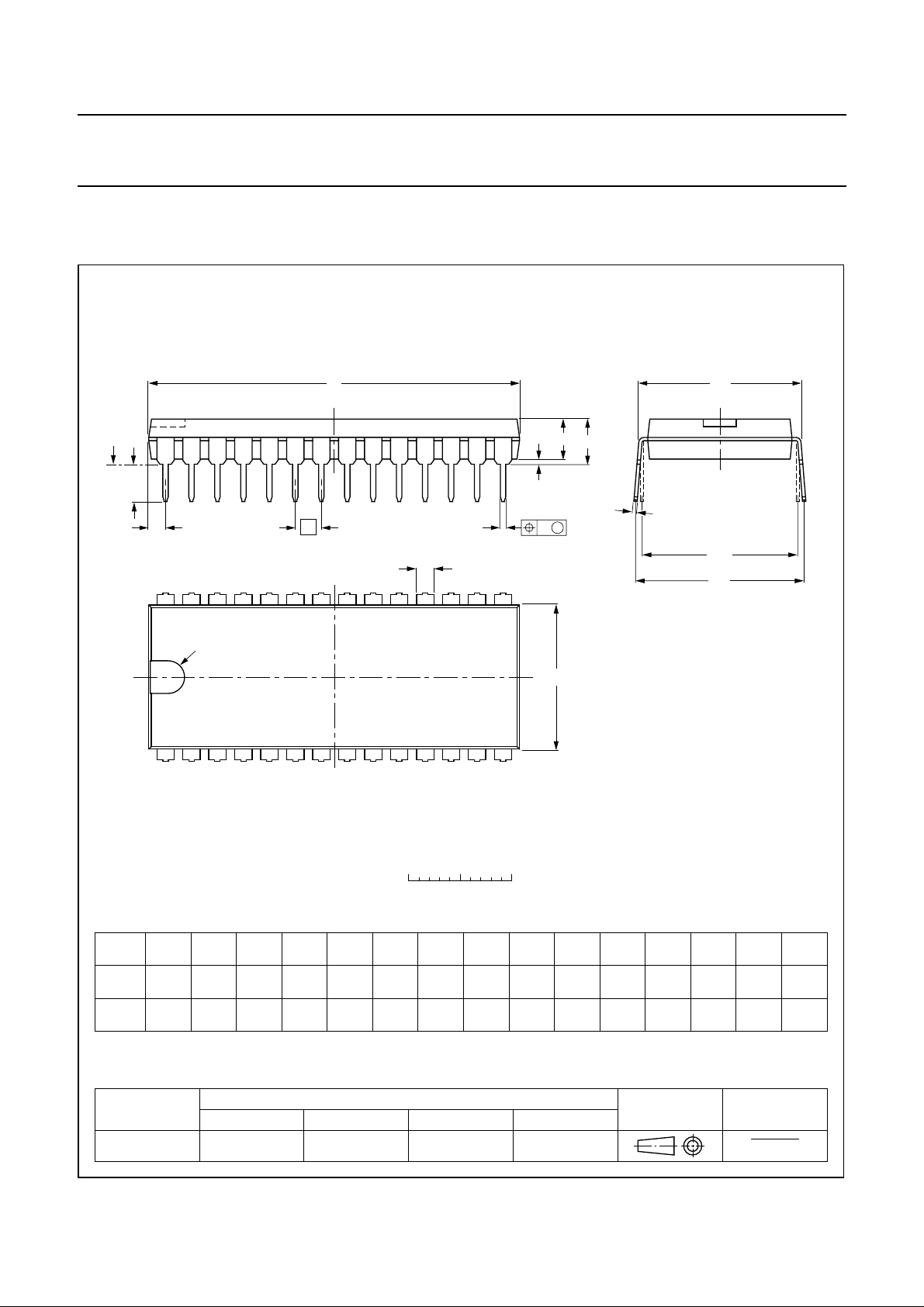
20 PACKAGE OUTLINES
handbook, full pagewidth
DIP28: plastic dual in-line package; 28 leads (600 mil)
D
seating plane
L
Z
28
e
b
PCA3351C; 52C; 53C;
PCD3351A; 52A; 53A
SOT117-1
M
E
A
2
A
A
1
w M
b
1
15
c
(e )
1
M
H
pin 1 index
1
0 5 10 mm
scale
DIMENSIONS (inch dimensions are derived from the original mm dimensions)
A
A
A
UNIT
inches
Note
1. Plastic or metal protrusions of 0.25 mm maximum per side are not included.
max.
mm
1 2
min.
max.
b
1.7
1.3
0.066
0.051
b
0.53
0.38
0.020
0.014
cD E weM
1
0.32
0.23
0.013
0.009
(1) (1)
36.0
35.0
1.41
1.34
14.1
13.7
0.56
0.54
E
14
(1)
L
3.9
3.4
M
15.80
15.24
0.62
0.60
H
E
17.15
15.90
0.68
0.63
0.252.54 15.24
0.010.10 0.60
e
1
0.15
0.13
Z
max.
1.75.1 0.51 4.0
0.0670.20 0.020 0.16
OUTLINE
VERSION
SOT117-1
IEC JEDEC EIAJ
051G05 MO-015AH
REFERENCES
1999 Oct 28 28
EUROPEAN
PROJECTION
ISSUE DATE
92-11-17
95-01-14

Philips Semiconductors Product specification
8-bit microcontrollers with DTMF generator
and 128 bytes EEPROM
SO28: plastic small outline package; 28 leads; body width 7.5 mm
D
c
y
Z
28
15
PCA3351C; 52C; 53C;
PCD3351A; 52A; 53A
SOT136-1
E
H
E
A
X
v M
A
pin 1 index
1
e
0 5 10 mm
DIMENSIONS (inch dimensions are derived from the original mm dimensions)
mm
A
max.
2.65
0.10
A
1
0.30
0.10
0.012
0.004
A2A3b
2.45
0.25
2.25
0.096
0.01
0.089
p
0.49
0.36
0.019
0.014
0.32
0.23
0.013
0.009
UNIT
inches
Note
1. Plastic or metal protrusions of 0.15 mm maximum per side are not included.
(1)E(1) (1)
cD
18.1
7.6
17.7
7.4
0.71
0.30
0.69
0.29
14
w M
b
p
scale
eHELLpQ
1.27
0.050
10.65
10.00
0.419
0.394
1.4
0.055
Q
A
2
0.043
0.016
A
1.1
0.4
L
p
L
0.25 0.1
0.01
(A )
1
detail X
1.1
0.25
1.0
0.043
0.01
0.039
A
3
θ
ywv θ
Z
0.9
0.4
0.035
0.004
0.016
o
8
o
0
OUTLINE
VERSION
SOT136-1
IEC JEDEC EIAJ
075E06 MS-013AE
REFERENCES
1999 Oct 28 29
EUROPEAN
PROJECTION
ISSUE DATE
95-01-24
97-05-22

Philips Semiconductors Product specification
8-bit microcontrollers with DTMF generator
and 128 bytes EEPROM
LQFP32: plastic low profile quad flat package; 32 leads; body 7 x 7 x 1.4 mm
c
y
X
24 17
25
16
Z
E
A
PCA3351C; 52C; 53C;
PCD3351A; 52A; 53A
SOT358-1
e
w M
b
p
e
1.45
1.35
pin 1 index
b
p
D
H
D
0.25
w M
cE
0.18
0.12
D
7.1
6.9
p
0.4
0.3
9
8
Z
D
B
0 2.5 5 mm
(1)
(1) (1)(1)
7.1
6.9
v M
v M
scale
eH
H
9.15
0.8
8.85
32
1
DIMENSIONS (mm are the original dimensions)
mm
A
A1A2A3b
max.
0.20
1.60
0.05
UNIT
Note
1. Plastic or metal protrusions of 0.25 mm maximum per side are not included.
D
E
A
B
9.15
8.85
H
E
LL
E
A
0.75
0.45
A
p
2
A
1
detail X
Z
D
0.25 0.11.0 0.2
0.9
0.5
(A )
L
p
L
Zywv θ
E
0.9
0.5
3
θ
o
7
o
0
OUTLINE
VERSION
SOT358 -1
IEC JEDEC EIAJ
REFERENCES
1999 Oct 28 30
EUROPEAN
PROJECTION
ISSUE DATE
95-12-19
97-08-04

Philips Semiconductors Product specification
8-bit microcontrollers with DTMF generator
and 128 bytes EEPROM
21 SOLDERING
21.1 Introduction
Thistextgivesaverybriefinsighttoacomplex technology.
A more in-depth account of soldering ICs can be found in
our
“Data Handbook IC26; Integrated Circuit Packages”
(document order number 9398 652 90011).
There is no soldering method that is ideal for all IC
packages. Wave soldering is often preferred when
through-holeandsurfacemount components are mixedon
one printed-circuit board. However, wave soldering is not
always suitable for surface mount ICs, or for printed-circuit
boards with high population densities. In these situations
reflow soldering is often used.
21.2 Through-hole mount packages
21.2.1 SOLDERING BY DIPPING OR BY SOLDER WAVE
The maximum permissible temperature of the solder is
260 °C; solder at this temperature must not be in contact
with the joints for more than 5 seconds. The total contact
time of successive solder waves must not exceed
5 seconds.
The device may be mounted up to the seating plane, but
the temperature of the plastic body must not exceed the
specified maximum storage temperature (T
printed-circuit board has been pre-heated, forced cooling
may be necessary immediately after soldering to keep the
temperature within the permissible limit.
21.2.2 MANUAL SOLDERING
Apply the soldering iron (24 V or less) to the lead(s) of the
package, either below the seating plane or not more than
2 mm above it. If the temperature of the soldering iron bit
is less than 300 °C it may remain in contact for up to
10 seconds. If the bit temperature is between
300 and 400 °C, contact may be up to 5 seconds.
21.3 Surface mount packages
21.3.1 REFLOW SOLDERING
Reflow soldering requires solder paste (a suspension of
fine solder particles, flux and binding agent) to be applied
totheprinted-circuitboardbyscreen printing, stencilling or
pressure-syringe dispensing before package placement.
Several methods exist for reflowing; for example,
infrared/convection heating in a conveyor type oven.
Throughput times (preheating, soldering and cooling) vary
between 100 and 200 seconds depending on heating
method.
stg(max)
). If the
PCA3351C; 52C; 53C;
PCD3351A; 52A; 53A
Typical reflow peak temperatures range from
215 to 250 °C. The top-surface temperature of the
packages should preferable be kept below 230 °C.
21.3.2 WAVE SOLDERING
Conventional single wave soldering is not recommended
forsurfacemountdevices(SMDs)orprinted-circuitboards
with a high component density, as solder bridging and
non-wetting can present major problems.
To overcome these problems the double-wave soldering
method was specifically developed.
If wave soldering is used the following conditions must be
observed for optimal results:
• Use a double-wave soldering method comprising a
turbulent wave with high upward pressure followed by a
smooth laminar wave.
• For packages with leads on two sides and a pitch (e):
– larger than or equal to 1.27 mm, the footprint
longitudinal axis is preferred to be parallel to the
transport direction of the printed-circuit board;
– smaller than 1.27 mm, the footprint longitudinal axis
must be parallel to the transport direction of the
printed-circuit board.
The footprint must incorporate solder thieves at the
downstream end.
• Forpackageswithleadsonfoursides, the footprint must
be placed at a 45° angle to the transport direction of the
printed-circuit board. The footprint must incorporate
solder thieves downstream and at the side corners.
During placement and before soldering, the package must
be fixed with a droplet of adhesive. The adhesive can be
applied by screen printing, pin transfer or syringe
dispensing. The package can be soldered after the
adhesive is cured.
Typical dwell time is 4 seconds at 250 °C.
A mildly-activated flux will eliminate the need for removal
of corrosive residues in most applications.
21.3.3 MANUAL SOLDERING
Fix the component by first soldering two
diagonally-opposite end leads. Use a low voltage (24 V or
less) soldering iron applied to the flat part of the lead.
Contact time must be limited to 10 seconds at up to
300 °C.
When using a dedicated tool, all other leads can be
soldered in one operation within 2 to 5 seconds between
270 and 320 °C.
1999 Oct 28 31

Philips Semiconductors Product specification
8-bit microcontrollers with DTMF generator
and 128 bytes EEPROM
21.4 Suitability of IC packages for wave, reflow and dipping soldering methods
MOUNTING PACKAGE
Through-hole mount DBS, DIP, HDIP, SDIP, SIL suitable
Surface mount BGA, LFBGA, SQFP, TFBGA not suitable suitable −
HBCC, HLQFP, HSQFP, HSOP, HTQFP,
HTSSOP, SMS
(4)
PLCC
LQFP, QFP, TQFP not recommended
SSOP, TSSOP, VSO not recommended
Notes
1. All surface mount (SMD) packages are moisture sensitive. Depending upon the moisture content, the maximum
temperature (with respect to time) and body size of the package, there is a risk that internal or external package
cracks may occur due to vaporization of the moisture in them (the so called popcorn effect). For details, refer to the
Drypack information in the
2. For SDIP packages, the longitudinal axis must be parallel to the transport direction of the printed-circuit board.
3. These packages are not suitable for wave soldering as a solder joint between the printed-circuit board and heatsink
(at bottom version) can not be achieved, and as solder may stick to the heatsink (on top version).
4. If wave soldering is considered, then the package must be placed at a 45° angle to the solder wave direction.
The package footprint must incorporate solder thieves downstream and at the side corners.
5. Wave soldering is only suitable for LQFP, QFP and TQFP packages with a pitch (e) equal to or larger than 0.8 mm;
it is definitely not suitable for packages with a pitch (e) equal to or smaller than 0.65 mm.
6. Wave soldering is only suitable for SSOP and TSSOP packages with a pitch (e) equal to or larger than 0.65 mm; it is
definitely not suitable for packages with a pitch (e) equal to or smaller than 0.5 mm.
, SO, SOJ suitable suitable −
“Data Handbook IC26; Integrated Circuit Packages; Section: Packing Methods”
not suitable
PCA3351C; 52C; 53C;
PCD3351A; 52A; 53A
SOLDERING METHOD
WAVE REFLOW
(2)
(3)
− suitable
suitable −
(4)(5)
suitable −
(6)
suitable −
(1)
DIPPING
.
22 DEFINITIONS
Data sheet status
Objective specification This data sheet contains target or goal specifications for product development.
Preliminary specification This data sheet contains preliminary data; supplementary data may be published later.
Product specification This data sheet contains final product specifications.
Limiting values
Limiting values given are in accordance with the Absolute Maximum Rating System (IEC 134). Stress above one or
more of the limiting values may cause permanent damage to the device. These are stress ratings only and operation
of the device at these or at any other conditions above those given in the Characteristics sections of the specification
is not implied. Exposure to limiting values for extended periods may affect device reliability.
Application information
Where application information is given, it is advisory and does not form part of the specification.
23 LIFE SUPPORT APPLICATIONS
These products are not designed for use in life support appliances, devices, or systems where malfunction of these
products can reasonably be expected to result in personal injury. Philips customers using or selling these products for
use in such applications do so at their own risk and agree to fully indemnify Philips for any damages resulting from such
improper use or sale.
1999 Oct 28 32

Philips Semiconductors Product specification
8-bit microcontrollers with DTMF generator
and 128 bytes EEPROM
NOTES
PCA3351C; 52C; 53C;
PCD3351A; 52A; 53A
1999 Oct 28 33

Philips Semiconductors Product specification
8-bit microcontrollers with DTMF generator
and 128 bytes EEPROM
NOTES
PCA3351C; 52C; 53C;
PCD3351A; 52A; 53A
1999 Oct 28 34

Philips Semiconductors Product specification
8-bit microcontrollers with DTMF generator
and 128 bytes EEPROM
NOTES
PCA3351C; 52C; 53C;
PCD3351A; 52A; 53A
1999 Oct 28 35

Philips Semiconductors – a w orldwide compan y
Argentina: see South America
Australia: 3 Figtree Drive, HOMEBUSH, NSW 2140,
Tel. +61 2 9704 8141, Fax. +61 2 9704 8139
Austria: Computerstr. 6, A-1101 WIEN, P.O. Box 213,
Tel. +43 1 60 101 1248, Fax. +43 1 60 101 1210
Belarus: Hotel Minsk Business Center, Bld. 3, r. 1211, Volodarski Str. 6,
220050 MINSK, Tel. +375 172 20 0733, Fax. +375 172 20 0773
Belgium: see The Netherlands
Brazil: see South America
Bulgaria: Philips Bulgaria Ltd., Energoproject, 15th floor,
51 James Bourchier Blvd., 1407 SOFIA,
Tel. +359 2 68 9211, Fax. +359 2 68 9102
Canada: PHILIPS SEMICONDUCTORS/COMPONENTS,
Tel. +1 800 234 7381, Fax. +1 800 943 0087
China/Hong Kong: 501 Hong Kong Industrial Technology Centre,
72 Tat Chee Avenue, Kowloon Tong, HONG KONG,
Tel. +852 2319 7888, Fax. +852 2319 7700
Colombia: see South America
Czech Republic: see Austria
Denmark: Sydhavnsgade 23, 1780 COPENHAGEN V,
Tel. +45 33 29 3333, Fax. +45 33 29 3905
Finland: Sinikalliontie 3, FIN-02630 ESPOO,
Tel. +358 9 615 800, Fax. +358 9 6158 0920
France: 51 Rue Carnot, BP317, 92156 SURESNES Cedex,
Tel. +33 1 4099 6161, Fax. +33 1 4099 6427
Germany: Hammerbrookstraße 69, D-20097 HAMBURG,
Tel. +49 40 2353 60, Fax. +49 40 2353 6300
Hungary: see Austria
India: Philips INDIA Ltd, Band Box Building, 2nd floor,
254-D, Dr. Annie Besant Road, Worli, MUMBAI 400 025,
Tel. +91 22 493 8541, Fax. +91 22 493 0966
Indonesia: PT Philips DevelopmentCorporation, SemiconductorsDivision,
Gedung Philips, Jl. Buncit Raya Kav.99-100, JAKARTA 12510,
Tel. +62 21 794 0040 ext. 2501, Fax. +62 21 794 0080
Ireland: Newstead, Clonskeagh, DUBLIN 14,
Tel. +353 1 7640 000, Fax. +353 1 7640 200
Israel: RAPAC Electronics, 7 Kehilat Saloniki St, PO Box 18053,
TEL AVIV 61180, Tel. +972 3 645 0444, Fax. +972 3 649 1007
Italy: PHILIPS SEMICONDUCTORS,Via Casati, 23 - 20052 MONZA (MI),
Tel. +39 039 203 6838, Fax +39 039 203 6800
Japan: Philips Bldg 13-37, Kohnan 2-chome, Minato-ku,
TOKYO 108-8507, Tel. +81 3 3740 5130, Fax. +81 3 3740 5057
Korea: Philips House, 260-199 Itaewon-dong, Yongsan-ku, SEOUL,
Tel. +82 2 709 1412, Fax. +82 2 709 1415
Malaysia: No. 76 Jalan Universiti, 46200 PETALING JAYA, SELANGOR,
Tel. +60 3 750 5214, Fax. +60 3 757 4880
Mexico: 5900 Gateway East, Suite 200, EL PASO, TEXAS 79905,
Tel. +9-5 800 234 7381, Fax +9-5 800 943 0087
Middle East: see Italy
Netherlands: Postbus 90050, 5600 PB EINDHOVEN, Bldg. VB,
Tel. +31 40 27 82785, Fax. +31 40 27 88399
New Zealand: 2 Wagener Place, C.P.O. Box 1041, AUCKLAND,
Tel. +64 9 849 4160, Fax. +64 9 849 7811
Norway: Box 1, Manglerud 0612, OSLO,
Tel. +47 22 74 8000, Fax. +47 22 74 8341
Pakistan: see Singapore
Philippines: Philips Semiconductors Philippines Inc.,
106 Valero St. Salcedo Village, P.O. Box 2108 MCC, MAKATI,
Metro MANILA, Tel. +63 2 816 6380, Fax. +63 2 817 3474
Poland: Al.Jerozolimskie 195 B, 02-222 WARSAW,
Tel. +48 22 5710 000, Fax. +48 22 5710 001
Portugal: see Spain
Romania: see Italy
Russia: Philips Russia, Ul. Usatcheva 35A, 119048 MOSCOW,
Tel. +7 095 755 6918, Fax. +7 095 755 6919
Singapore: Lorong 1, Toa Payoh, SINGAPORE 319762,
Tel. +65 350 2538, Fax. +65 251 6500
Slovakia: see Austria
Slovenia: see Italy
South Africa: S.A. PHILIPS Pty Ltd., 195-215 Main Road Martindale,
2092 JOHANNESBURG, P.O. Box 58088 Newville 2114,
Tel. +27 11 471 5401, Fax. +27 11 471 5398
South America: Al. Vicente Pinzon, 173, 6th floor,
04547-130 SÃO PAULO, SP, Brazil,
Tel. +55 11 821 2333, Fax. +55 11 821 2382
Spain: Balmes 22, 08007 BARCELONA,
Tel. +34 93 301 6312, Fax. +34 93 301 4107
Sweden: Kottbygatan 7, Akalla, S-16485 STOCKHOLM,
Tel. +46 8 5985 2000, Fax. +46 8 5985 2745
Switzerland: Allmendstrasse 140, CH-8027 ZÜRICH,
Tel. +41 1 488 2741 Fax. +41 1 488 3263
Taiwan: Philips Semiconductors, 6F, No. 96, Chien Kuo N. Rd., Sec. 1,
TAIPEI, Taiwan Tel. +886 2 2134 2886, Fax. +886 2 2134 2874
Thailand: PHILIPS ELECTRONICS (THAILAND) Ltd.,
209/2 Sanpavuth-Bangna Road Prakanong, BANGKOK 10260,
Tel. +66 2 745 4090, Fax. +66 2 398 0793
Turkey: Yukari Dudullu, Org. San. Blg., 2.Cad. Nr. 28 81260 Umraniye,
ISTANBUL, Tel. +90 216 522 1500, Fax. +90 216 522 1813
Ukraine: PHILIPS UKRAINE, 4 Patrice Lumumba str., Building B, Floor 7,
252042 KIEV, Tel. +380 44 264 2776, Fax. +380 44 268 0461
United Kingdom: Philips Semiconductors Ltd., 276 Bath Road, Hayes,
MIDDLESEX UB3 5BX, Tel. +44 208 730 5000, Fax. +44 208 754 8421
United States: 811 East Arques Avenue, SUNNYVALE, CA 94088-3409,
Tel. +1 800 234 7381, Fax. +1 800 943 0087
Uruguay: see South America
Vietnam: see Singapore
Yugoslavia: PHILIPS, Trg N. Pasica 5/v, 11000 BEOGRAD,
Tel. +381 11 62 5344, Fax.+381 11 63 5777
For all other countries apply to: Philips Semiconductors,
International Marketing & Sales Communications, Building BE-p, P.O. Box 218,
5600 MD EINDHOVEN, The Netherlands, Fax. +31 40 27 24825
© Philips Electronics N.V. SCA
All rights are reserved. Reproduction in whole or in part is prohibited without the prior written consent of the copyright owner.
The information presented in this document does not form part of any quotation or contract, is believed to be accurate and reliable and may be changed
without notice. No liability will be accepted by the publisher for any consequence of its use. Publication thereof does not convey nor imply any license
under patent- or other industrial or intellectual property rights.
1999
Internet: http://www.semiconductors.philips.com
68
Printed in The Netherlands 465002/07/pp36 Date of release: 1999 Oct 28 Document order number: 9397 750 06528
 Loading...