

Page 1

查询PCA2000供应商
INTEGRATED CIRCUITS
DATA SH EET
PCA2000; PCA2001
32 kHz watch circuit with
programmable adaptive motor
pulse
Product specification
Supersedes data of 2003 Feb 04
2003 Dec 17
Page 2

Philips Semiconductors Product specification
32 kHz watch circuit with programmable
adaptive motor pulse
FEATURES
• Amplitude-regulated 32 kHz quartz crystal oscillator,
with excellent frequency stability and high immunity to
leakage currents
• Electrically programmable time calibration with 1 ppm
resolution stored in One Time Programmable (OTP)
memory
• The quartz crystal is the only external component
connected
• Very low power consumption, typical 90 nA
• One second output pulses for bipolar stepping motor
• Minimum power consumption for the entire watch, due
to self adaptation of the motor drive according to the
required torque
• Reliable step detection circuit
• Motor pulse width, pulse modulation, and pulse
adaptation rangeprogrammable in a wide range, stored
in OTP memory
• Stopfunction for accuratetimesetting and power saving
during shelf life
• End Of Life (EOL) indication for silver oxide or lithium
battery (only the PCA2000 has the EOL feature)
• Test mode for accelerated testing of the mechanical
parts and the IC.
PCA2000; PCA2001
GENERAL DESCRIPTION
The PCA2000; PCA2001 are CMOS integrated circuitsfor
battery operated wrist watches with a 32 kHz quartz
crystal as timing element and a bipolar 1 Hz stepping
motor. The quartz crystal oscillator and the frequency
divider are optimized for minimum power consumption.
A timing accuracy of 1 ppm is achieved with a
programmable, digital frequency adjustment.
To obtain the minimum overall power consumption for the
watch, an automatic motor pulse adaptation function is
provided. The circuit supplies only the minimum drive
current,which is necessarytoensure a correctmotor step.
Changing the drive current of the motor is achieved by
chopping the motor pulse with a variable duty cycle. The
pulsewidth and the range of the variable duty cycle can be
programmedtosuit different types of motor. Theautomatic
pulse adaptation scheme is based on a safe dynamic
detection of successful motor steps.
Apad RESET is provided(used for stoppingthe motor) for
accurate time setting and for accelerated testing of the
watch.
The PCA2000 has a battery EOL warning function. If the
battery voltage drops below the EOL threshold voltage
(which can be programmed for silver oxide or lithium
batteries), the motor steps change from one pulse per
second to a burst of four pulses every 4 seconds.
APPLICATIONS
• Driver circuits for bipolar stepping motors
• High immunity motor drive circuits.
ORDERING INFORMATION
TYPE NUMBER
NAME DESCRIPTION VERSION
PCA2000U/AA − bare die; chip in tray −
PCA2001U/AA − bare die; chip in tray −
PCA2000U/10AA − bare die; chip on film frame carrier −
PCA2001U/10AA − bare die; chip on film frame carrier −
The PCA2001 uses the same circuit as the PCA2000, but
without the EOL function.
PACKAGE
2003 Dec 17 2
Page 3

Philips Semiconductors Product specification
32 kHz watch circuit with programmable
adaptive motor pulse
BLOCK DIAGRAM
DD
SS
3
4
5
1
2
OSCILLATOR
VOLTAGE DETECTOR,
OTP-CONTROLLER
÷4
TIMING ADJUSTMENT,
EOL
PCA2000 only
PCA2000
PCA2001
OSCIN
OSCOUT
V
V
TEST
8 kHz
INHIBITION
OTP-MEMORY
32 Hz
DIVIDER RESET
MOTOR CONTROL WITH
ADAPTIVE PULSE MODULATION
DETECTION
STEP
PCA2000; PCA2001
8
RESET
reset
1 Hz
PINNING
SYMBOL PAD DESCRIPTION
V
SS
1 ground
TEST 2 test output
OSCIN 3 oscillator input
OSCOUT 4 oscillator output
V
DD
5 supply voltage
MOT1 6 motor 1 output
MOT2 7 motor 2 output
RESET 8 reset input
67
Fig.1 Block diagram.
handbook, halfpage
OSCOUT
V
SS
TEST
OSCIN
mgw567
MOT2MOT1
1
2
8
7
PCA2000
PCA2001
3
4
6
5
MGU554
Fig.2 Pad configuration.
RESET
MOT2
MOT1
V
DD
2003 Dec 17 3
Page 4

Philips Semiconductors Product specification
32 kHz watch circuit with programmable
adaptive motor pulse
FUNCTIONAL DESCRIPTION
Motor pulse
The motor output supplies pulses of different driving
stages, depending on the torque required to turn on the
motor. The number of different stages can be selected
between three and six. With the exception of the highest
driving stage, each motor pulse (tp in Figs 3 and 6) is
followed by a detection phase during which the motor
movement is monitored, in order to check whether the
motor has turned correctly or not.
If a missing step is detected, a correction sequence is
generated (see Fig.3) and the driving stage is switched to
the next level. The correction sequence consists of two
pulses: first a short pulse in the opposite direction
(0.98 ms, modulated withthe maximumduty cycle) to give
the motor a defined position, followed by a motor pulse of
the strongest driving level. Every 4 minutes, the driving
level is lowered again by one stage.
The motor pulse has a constant pulse width. The driving
level is regulated by chopping the driving pulse with a
variable duty cycle. The driving level starts from the
programmedminimumvalue and increases by6.25%after
each failed motor step. The strongest driving stage, which
is not followed by a detection phase, is programmed
separately.
PCA2000; PCA2001
Therefore, it is possible to program a larger energy gap
between the pulses with step detection and the strongest,
not monitored, pulse. This might be necessary to ensure a
reliable and stable operation under adverse conditions
(magnetic fields, vibrations). If the watch works in the
highest driving stage, the driving level jumps after the
4-minute period directly to the lowest stage, and not just
one stage lower.
To optimize the performance for different motors, the
following parameters can be programmed:
• Pulse width: 0.98 to 7.8 ms in steps of 0.98 ms
• Duty cycle of lowest driving level: 37.5% to 56.25% in
steps of 6.25%
• Number of driving levels (including the highest driving
level): 3 to 6
• Duty cycle of the highest driving level: 75% or 100%
• Enlargement pulse forthe highestdriving level: on or off.
The enlargement pulse has a duty cycle of 25% and a
pulse width which is twice the programmed motor pulse
width. The repetition period for the chopping pattern is
0.98 ms. Figure 4 shows an example of a 3.9 ms pulse.
handbook, full pagewidth
1.96 ms
t
p
detection phase
31.25 ms
0.98 ms
31.25 ms
Fig.3 Correction sequence after failed motor step.
2003 Dec 17 4
t
p
2t
p
MGW350
Page 5
Philips Semiconductors Product specification
32 kHz watch circuit with programmable
adaptive motor pulse
handbook, full pagewidth
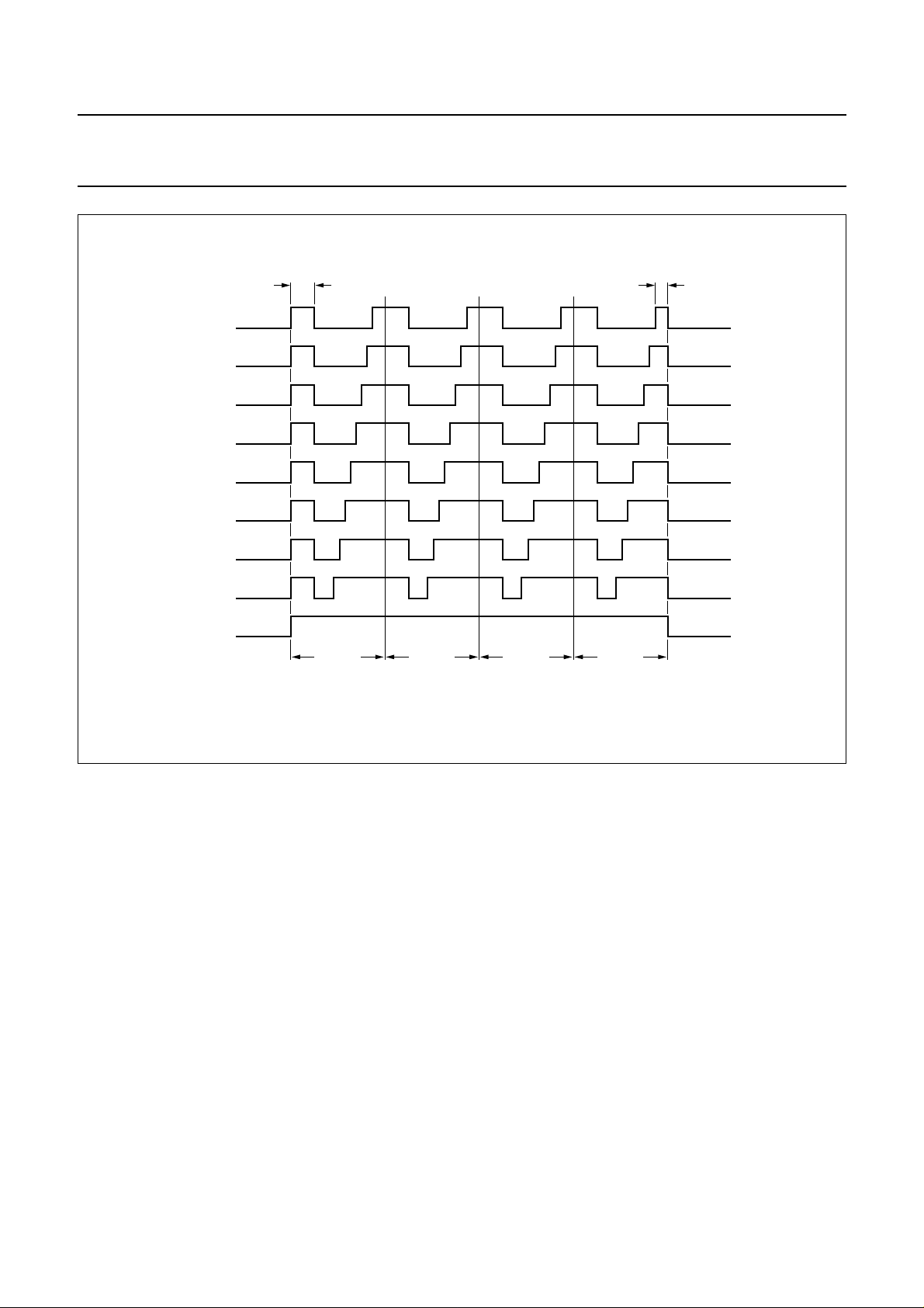
DUTY CYCLE
37.5%
43.75%
50%
56.25%
62.5%
68.75%
75%
81.25%
0.244 ms 0.122 ms
PCA2000; PCA2001
100%
Fig.4 Possible modulations for a 3.9 ms motor pulse.
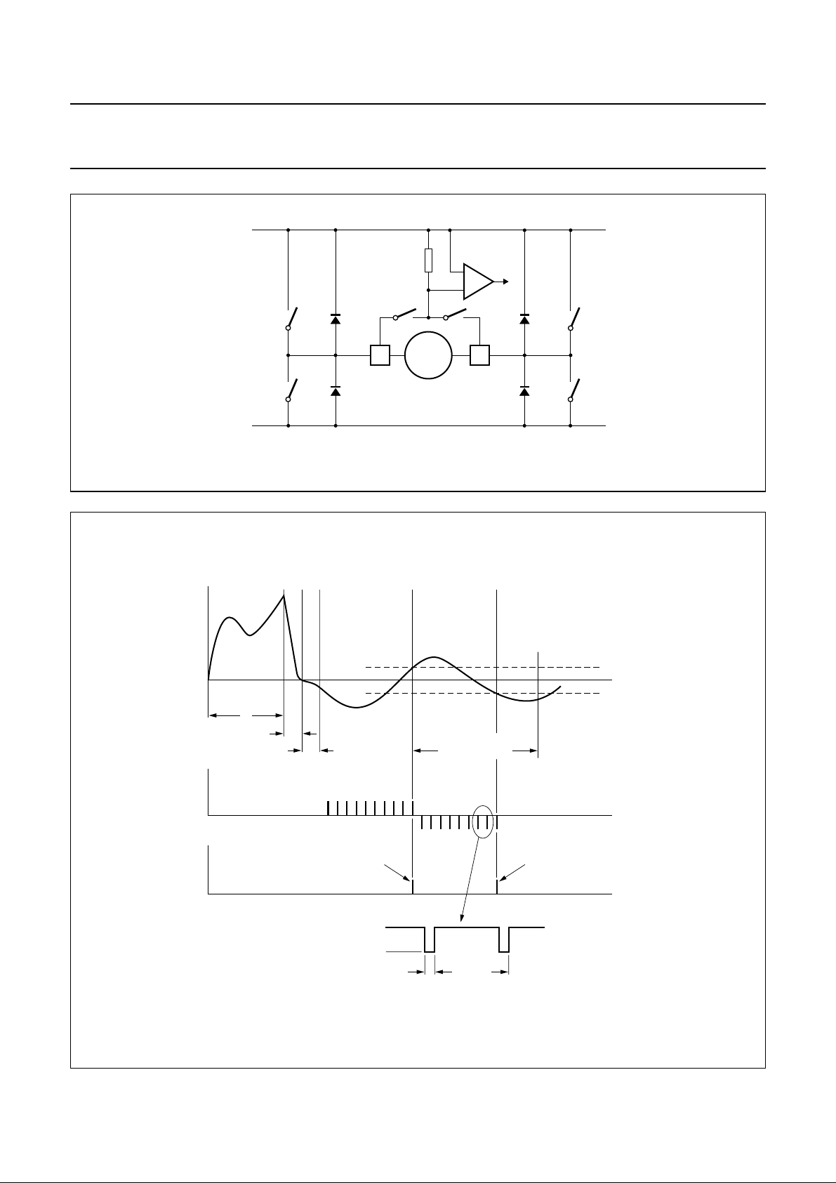
Step detection
Figure 5 shows a simplified diagram of the motor driving
and step detection circuit, and Fig.6 shows the step
detection sequence and corresponding sampling current.
Betweenthe motor driving pulses,theswitches P1 and P2
are closed, which means the motor is short-circuited. For
a pulse in one direction, P1 and N2 are open, and
P2 and N1 are closed with the appropriate duty cycle; for
a pulse inthe opposite direction, P2 and N1 are open, and
P1 and N2 closed.
Thestep detection phaseisinitiated after themotor driving
pulse (see Fig.3). P1 and P2 are first closed for 0.98 ms
and then all four drive switches (P1, N1, P2 and N2) are
opened for 0.98 ms.
As a result, the energy stored in the motor inductance is
reduced as fast as possible.
0.98 ms0.98 ms0.98 ms 0.98 ms
MGW351
The induced current caused by the residual motor
movement is thensampled in phase 3(closing P3 and P2)
and in phase 4 (closing P1 and P4). For step detection in
the opposite direction P1 and P4 are closed during
phase 3 and P2 and P3 during phase 4 (see Fig.6).
The condition fora successful motorstep is a positive step
detection pulse (current in the same direction as in the
driving phase) followed by a negative detection pulse
withinagiven time limit. This timelimitcanbeprogrammed
between 3.9 and 10.7 ms (in steps of 0.98 ms) in order to
ensure a safe and correct step detection under all
conditions (for instance magnetic fields). The step
detection phase stops after the last 31.25 ms, after the
start of the motor driving pulse.
2003 Dec 17 5
Page 6
Philips Semiconductors Product specification
32 kHz watch circuit with programmable
adaptive motor pulse
V
handbook, full pagewidth
DD
P1
MOT1
N1
V
SS
Fig.5 Simplified diagram of motor driving and step detection circuit.
R
D
MOTOR
PCA2000; PCA2001
D1
P4P3
MOT2
P2
N2
MGW352
handbook, full pagewidth
I
MOT
sampling
voltage
sampling
voltage
t
p
0.98 ms
(motor shorted)
sampling results
phase 1
phase 2
positive detection
motor shorted
phase 3
td = 0.98 ms
sampling
sampling
61 µs
phase 4
programmable time limit
OTP C4 to C6
negative detection
0.49 ms
positive detection level
t
negative detection level
t
t
MGW569
Fig.6 Step detection sequence and corresponding sampling voltage.
2003 Dec 17 6
Page 7

Philips Semiconductors Product specification
1
1
32 kHz watch circuit with programmable
adaptive motor pulse
Time calibration
Thequartz crystal oscillatorhas an integratedcapacitance
of 5.2 pF, which is lower than the specified capacitance
(CL) of 8.2 pF for the quartz crystal. Therefore, the
oscillator frequency is typically 60 ppm higher than
32.768 kHz.Thispositivefrequency offset is compensated
by removing the appropriate number of 8192 Hz pulses in
the divider chain (maximum 127 pulses), every
1 or 2 minutes. The time correction is given in Table 1.
After measuring the effective oscillator frequency, the
numberof correction pulses must becalculatedand stored
together with the calibration period in the OTP memory
(see Section “Programming the memory cells”).
The oscillator frequency canbe measured at pad RESET,
where a square wave signal with the frequency of
f
×
------------ 1024
This frequency shows a jitter every minute or every two
minutes,dependingontheprogrammedcalibrationperiod,
which originates from the time calibration.
Detailson how to measuretheoscillator frequency and the
programmed inhibit time are given in Section
“Measurement of oscillator frequency and inhibit time”.
is provided.
osc
PCA2000; PCA2001
Reset
At pin RESET an output signal with a frequency of
f
×
------------ -
1024
Connecting pad RESET to VDDstops the motor drive and
opens all four (P1, N1, P2 and N2) driver switches (see
Fig.5). Connecting pad RESET to VSS activates the test
mode. In this mode the motor output frequency is 32 Hz,
which can be used to test the mechanical function of the
watch.
After releasing the pad RESET, the motor starts exactly
one second later with the smallest duty cycle and with the
opposite polarity to the last pulse before stopping.
The debounce time for the RESET function is between
31 and 62 ms.
Programming possibilities
The programming data is stored in OTP cells (EPROM
cells). At delivery,all memory cellsare in state 0. The cells
can be programmed to the state 1, but then there is no
more set back to state 0.
The programming data is organized in an array of three
8-bit words: word A contains the time calibration, and
words B and C contain the setting for the monitor pulses
(see Table 2).
= 32 Hz is provided.
osc
Table 1 Time calibration
CALIBRATION PERIOD
1 minute 2.03 0.176 258 22.3
2 minutes 1.017 0.088 129 11.15
Table 2 Words and bits
WORD
12345678
A number of 8192 Hz pulses to be removed calibration
B lowest stage: duty cycle number of driving stages highest stage:
C pulse width maximum time delaybetweenpositive
CORRECTION PER STEP (n = 1) CORRECTION PER STEP (n = 127)
ppm seconds per day ppm seconds per day
BIT
period
factory test bit
duty cycle and
stretching
and negative detection pulses
EOL
voltage
factorytest
bit
2003 Dec 17 7
Page 8

Philips Semiconductors Product specification
32 kHz watch circuit with programmable
adaptive motor pulse
Table 3 Description of word A bits
BIT VALUE DESCRIPTION
Inhibit time
1to7 − Adjust the number of the 8192 Hz
pulses to be removed. Bit 1 is the
MSB and bit 7 is the LSB.
Calibration period
8 0 1 minute
1 2 minutes
Table 4 Description of word B bits
BIT VALUE DESCRIPTION
Duty cycle lowest driving stage
1 to 2 00 37.5%
01 43.75%
10 50%
11 56.25%
Number of driving stages
3 to 4 00 3
01 4
10 5
11 6; note 1
Duty cycle highest driving stage
5 0 75%; note 2
1 100%
Stretching pulse
6 0 pulse is not stretched
1 pulse of 2t
is added
Factory test bits
7to8 −
and duty cycle of 25%
pr
PCA2000; PCA2001
Table 5 Description of word C bits
BIT VALUE DESCRIPTION
Pulse width tpr(ms)
1 to 3 000 0.98
001 1.95
010 2.90
011 3.90
100 4.90
101 5.90
110 6.80
111 7.80
Time delay t
4 to 6 000 3.91
EOL voltage of the battery
7 0 1.38 V (silver-oxide)
Factory test bit
8 −
Note
1. Between positive and negative detection pulses.
(ms); note 1
max
001 4.88
010 5.86
011 6.84
100 7.81
101 8.79
110 9.77
111 10.74
1 2.5 V (lithium)
Notes
1. Including the highest driving stage, which one has no
motor step detection.
2. If the maximum duty cycle of 75% is selected, not all
programming combinations are possible since the
second highest level must be smaller than the highest
driving level.
2003 Dec 17 8
Page 9

Philips Semiconductors Product specification
32 kHz watch circuit with programmable
adaptive motor pulse
Programming procedure
For a watchit isessential that the timing calibration can be
made after the watch is fully assembled. In this situation,
the supply pads are often the only terminals which are still
accessible.
Writing to the OTP cells and performing the related
functional checks is achieved in the PCA2000; PCA2001
by modulating the supply voltage. The necessary control
circuit consists basically of a voltage level detector, an
instruction counter which determines the function to be
performed, and an 8-bit shift register which allows writing
to the OTP cells of an 8-bit word in one step and acts as a
data pointer for checking the OTP content.
There are five different instruction states (states 3 and 5
are handled as state 4):
• State 1: measurement of the quartz crystal oscillator
frequency (divided by 1024)
• State 2: measurement of the inhibit time
• State 3: write/check word A
• State 4: write/check word B
• State 5: write/check word C.
Each instruction state is switched on with a pulse to
VP(6.7 V). After this large pulse, an initial waiting time of
t0(20 ms) is required. The programming instructions are
then entered by modulating the supply voltage with small
pulses (amplitude V
t
=30µs). The first small pulse defines the start time,
mod
the following pulses perform three different functions,
depending on the delay from the preceding pulse
(see Figs 7, 8, 11, and 12):
• t1= 0.7 ms: increments the instruction counter
• t2= 1.7 ms: clocks the shift register with data = logic 0
• t3= 2.7 ms: clocks the shift register with data = logic 1.
The programming procedure requires a stable oscillator.
This means that a waiting time, determined by the start-up
time of the oscillator is necessary after power-up of the
circuit.
= 0.35 V and pulse width
P(mod)
PCA2000; PCA2001
Programming the memory cells
Applying the two-stage programming pulse (see Fig.7)
transfers the stored data in the shift register to the OTP
cells.
Perform the following to program a memory word:
1. Starting with a V
thenset the instructioncounterto the wordyouwant to
write (td = t1).
2. Enter the data you want to store in the shift register
(td=t2or t3). Enter the LSB first (bit 8) and the MSB
last (bit 1).
3. Applythetwo-stageprogrammingpulse(V
V
) stores the word. The delay between the last
store
data bit and the pre-store pulse (V
The example shown in Fig.7 performs the following
functions:
• Start
• Setting instruction counter to state 4 (word B)
• Entering data word 110101 into the shift register
(sequence: first bit 6 and last bit 1)
• Writing to the OTP cells for word B.
General start up sequence
You must follow the sequence belowto ensure the correct
operation at start up:
1. Apply the supply voltage to the circuit.
2. Wait for at least 2 seconds.
3. Connect the pad RESET to VDDfor a minimum of 62
ms (this activates the stop mode).
4. Disconnect the pad RESET from VDD(this resets the
circuit to normal operating mode).
After this sequence the memory contents are read
immediately and the programmed options are set. This
sequence also resets all major circuit blocks and ensures
that they function correctly.
pulse wait for the time period t
P(start)
pre-store
pre-store
then
) is td=t4.
0
After the V
pulse, the instruction counter is in state 1
P(start)
and the data shift register is cleared.
The instruction state ends with a second pulse to V
or with a pulse to V
store
.
P(stop)
In any case, the instruction states are terminated
automatically 2 seconds after the last V
DD(mod)
pulse.
2003 Dec 17 9
Page 10

Philips Semiconductors Product specification
32 kHz watch circuit with programmable
adaptive motor pulse
handbook, full pagewidth
V
DD(mod)
V
P(start)
V
P(mod)
t
p(start)
t1t1t1t
t
0
V
DD
V
SS
t
3
2
PCA2000; PCA2001
t
pre-store
V
store
V
pre-store
t
t
3
t
2
t3t
3
4
t
store
MGW356
Fig.7 Supply voltage modulation for programming.
Checking memory content
The stored data of the OTP array can be checked bit wise
by measuring the supply current. The array word is
selected by the instruction state and the bit is addressed
by the shift register.
To read a word, the word is first selected (pulse
distance t1), and a logic 1 is written into the first cell of the
shiftregister (pulse distance t3). This logic 1 is then shifted
through the entire shift register (pulse distance t2), so that
it points with each clock pulse to the next bit.
If the addressed OTP cell contains a logic 1, a 30 kΩ
resistor is connected between VDD and VSS, which
increases the supply current accordingly.
Figure 8 shows the supply voltage modulation for reading
word B,with the correspondingsupply current variationfor
word B = 110101 (sequence: first MSB and last LSB).
2003 Dec 17 10
Page 11

Philips Semiconductors Product specification
32 kHz watch circuit with programmable
adaptive motor pulse
V
(1) ∆I
DD
=
V
DD
--------------- 30 kΩ
DD(mod)
V
P(start)
V
P(mod)
V
DD
V
SS
I
DD
t
p(start)
t
t1t
0
t
t
1
3
1
(1)
t
t2t2t2t
2
V
P(stop)
PCA2000; PCA2001
t
p(stop)
2
mgw357
Fig.8 Supply voltage modulation and corresponding supply current variation for reading word B.
Frequency tuning of assembled watch
Figure 9 shows the test set-up for frequency tuning the assembled watch.
handbook, full pagewidth
32 kHz
FREQUENCY
COUNTER
PROGRAMMABLE
DC POWER SUPPLY
PC INTERFACE
PCA200x
M
motor
battery
PC
Fig.9 Frequency tuning at assembled watch.
2003 Dec 17 11
MGW568
Page 12

Philips Semiconductors Product specification
32 kHz watch circuit with programmable
adaptive motor pulse
Measurement of oscillator frequency and inhibit time
The output of the two measuring states can either be
monitored directly atpad RESET or asa modulation of the
supply voltage (a modulating resistor of 30 kΩ is
connected between VDD and VSS when the signal at
pad RESET is at HIGH-level).
You must follow the supply voltage modulation (see
Fig.10)) in order to guarantee the correct start up of the
circuit during production and testing.
t
V
V
DD(nom)
DD
t
(start)
V
SS
V
> 500 ms
Fig.10 Supply voltageat start up during production
and testing.
p(stop)
P(stop)
001aaa055
PCA2000; PCA2001
Customer testing
Connecting pad RESET to VSSactivates the test mode. In
thistestmode, the motor output frequencyis8 Hz;theduty
cycle reduction and battery check occurs every second,
instead of every 4 minutes. If the supply voltage drops
below the EOL threshold voltage, the motor output
frequency is 32 Hz with the highest driving level.
EOL of battery
The supply voltage is checked every 4 minutes. If it drops
below the EOL reference (1.38 V for silver-oxide, 2.5 V for
lithium batteries), the motor steps change from one pulse
per second to a burst of four pulses every 4 seconds. The
step detection is switched off, and the motor is driven with
the highest pulse level.
Only the PCA2000 has an EOL function.
V
P(start)
V
DD
t
p(start)
t
t
0
1
V
P(stop)
t
p(stop)
handbook, halfpage
Measuring states:
• State 1: quartz crystal oscillator frequency divided by
1024; state 1 starts with a pulse to VP and ends with a
second pulse to V
P
• State 2: inhibit time (see Figs 11 and 12); a signal with
periodicity of 31.25 + n × 0.122 ms appears at
pad RESET and as current modulation at pad VDD.
handbook, halfpage
V
V
DD
SS
31.25 ms + inhibition time
MGW355
Fig.11 Output waveform at pad RESET for
instruction state 2.
V
V
DD(nom)
V
SS
P(mod)
MGU719
Fig.12 Supply voltage modulation for starting and
stopping of instruction state 2.
2003 Dec 17 12
Page 13

Philips Semiconductors Product specification
32 kHz watch circuit with programmable
PCA2000; PCA2001
adaptive motor pulse
LIMITING VALUES
In accordance with the Absolute Maximum Rating System (IEC 60134).
SYMBOL PARAMETER CONDITIONS MIN. MAX. UNIT
V
DD
V
i
T
amb
T
stg
t
o(sc)
Notes
1. For writing to the OTP cells, the supply voltage VDD can be raised to a maximum of 12 V for a period of 1 second.
2. Connecting the battery with reversed polarity does not destroy the circuit, but in this condition a large current flows,
which rapidly discharges the battery.
HANDLING
Inputs and outputs are protected against electrostatic discharges in normal handling. However to be totally safe, it is
advised to undertake handling precautions appropriate to handling MOS devices. Advice can be found in
“Data handbook IC16: General; handling MOS devices”
supply voltage VSS= 0 V; notes 1 and 2 −1.8 +7.0 V
all input voltages VSS− 0.5 VDD+ 0.5 V
ambient temperature −10 +60 °C
storage temperature −30 +100 °C
output short-circuit duration indefinite s
.
CHARACTERISTICS
VDD= 1.55 V;VSS=0V;f
= 32.768 kHz; T
osc
=25°C; quartz crystal: RS=40kΩ,C1= 2 to 3 fF, CL= 8.2 pF; unless
amb
otherwise specified.
SYMBOL PARAMETER CONDITIONS MIN. TYP. MAX. UNIT
Supply
V
∆V
I
DD
DD
DD
supply voltage normal operating mode;
T
= −10 to +60 °C
amb
supply voltage variation ∆V/∆t=1V/µs −−0.25 V
supply current between motor pulses − 90 120 nA
1.10 1.55 3.60 V
between motor pulses at VDD= 3.5 V − 120 180 nA
T
= −10 to +60 °C −−200 nA
amb
stop mode; pad RESET connected to VDD− 100 135 nA
Motor output
V
sat
Z
sc
saturation voltage RM=2kΩ; T
= −10 to +60 °C; note 1 − 150 200 mV
amb
short-circuit impedance between motor pulses; I
<1mA − 200 300 Ω
motor
Oscillator
V
g
t
start
m
osc
starting voltage 1.1 −−V
transconductance V
≤ 50 mV (p-p) 5 10 −µS
OSCIN
start-up time − 0.3 0.9 s
∆f/f frequency stability ∆VDD= 100 mV − 0.05 0.20 ppm
C
int
R
par
integrated load capacitance 4.3 5.2 6.3 pF
parasitic resistance allowed resistance between adjacent pads 20 −−MΩ
2003 Dec 17 13
Page 14

Philips Semiconductors Product specification
32 kHz watch circuit with programmable
PCA2000; PCA2001
adaptive motor pulse
SYMBOL PARAMETER CONDITIONS MIN. TYP. MAX. UNIT
Voltage level detector
V
th(EOL)
TC
EOL
Pad RESET
f
o
∆V
o
tr,t
f
I
i(AV)
Notes
1. Σ (P + N).
2. RLand CL are a load resistor and load capacitor, externally connected to pad RESET.
Table 6 Specifications for OTP programming (see Figs 7, 8 and 12).
SYMBOL PARAMETER
V
DD
V
P(start)
V
P(stop)
V
P(mod)
V
pre-store
V
store
I
store
t
p(start)
t
p(stop)
t
mod
t
pre-store
t
store
t
0
t
1
t
2
t
3
t
4
SR slew rate for modulation of the supply voltage 0.5 − 5.0 V/µs
R
read
EOL threshold voltage silver-oxide battery 1.30 1.38 1.46 V
lithium battery 2.35 2.50 2.65 V
temperature coefficient −−0.07 − %/°C
output frequency − 32 − Hz
output voltage swing RL=1MΩ; CL= 10 pF; note 2 1.4 −−V
rise and fall time RL=1MΩ; CL= 10 pF; note 2 − 1 −µs
average input current pad RESET connected to VDD or V
(1)
SS
− 10 20 nA
MIN. TYP. MAX. UNIT
supply voltage during programming procedure 1.5 − 3.0 V
supply voltage for starting programming procedure 6.6 − 6.8 V
supply voltage for stopping programming procedure 6.2 − 6.4 V
supply voltage modulation for entering instructions 320 350 380 mV
supply voltage for pre-store pulse 6.2 − 6.4 V
supply voltage for writing to the OTP cells 9.9 10.0 10.1 V
supply current for writing to the OTP cells −−10 mA
pulse width of start pulse 8 10 12 ms
pulse width of stop pulse 0.05 − 0.5 ms
modulation pulse width 25 30 40 µs
pulse width of pre-store pulse 0.05 − 0.5 ms
pulse width for writing to the OTP cells 95 100 110 ms
waiting time after start pulse 20 − 30 ms
pulse distance for incrementing the state counter 0.6 0.7 0.8 ms
pulse distance for clocking the data register with data = logic 0 1.6 1.7 1.8 ms
pulse distance for clocking the data register with data = logic 1 2.6 2.7 2.8 ms
waiting time for writing to OTP cells 0.1 0.2 0.3 ms
supply current modulation read-out resistor 18 30 45 kΩ
Note
1. Program each word once only.
2003 Dec 17 14
Page 15

Philips Semiconductors Product specification
32 kHz watch circuit with programmable
adaptive motor pulse
BONDING PAD LOCATIONS
SYMBOL PAD
COORDINATES
xy
(3)
V
SS
TEST
(2)
1 −480 +330
2 −480 +160
OSCIN 3 −480 −160
OSCOUT 4 −480 −330
V
DD
5 +480 −330
MOT1 6 +480 −160
MOT2 7 +480 +160
RESET 8 +480 +330
Notes
1. All coordinates are referenced, in µm, to the centre of
the die (see Fig.13).
2. Pad TESTisusedfor factory tests; in normal operation
it should be left open-circuit, and it has an internal
pull-down resistance to VSS.
3. The substrate (rear side of the chip) is connected to
VSS. Therefore the die pad must be either floating or
connected to VSS.
(1)
PCA2000; PCA2001
Table 7 Mechanical chip data; note 1
PARAMETER VALUE
Bonding pad:
metal 96 × 96 µm
opening 86 × 86 µm
Thickness:
chip for bonding 200 ±25 µm
chip for golden bumps 270 ±25 µm
Bumps:
height 25 ±5 µm
Note
1. The substrate of the chip is connected to VSS.
handbook, halfpage
0.90 mm
OSCOUT
1.20 mm
V
1
SS
TEST
OSCIN
2
3
4
y
x
0
0
MGW353
Fig.13 Bonding pad locations.
8
7
PC2000
PC2001
6
5
RESET
MOT2
MOT1
V
DD
2003 Dec 17 15
Page 16

Philips Semiconductors Product specification
32 kHz watch circuit with programmable
adaptive motor pulse
TRAY INFORMATION
handbook, full pagewidth
x
y
F
G
H
1,1 x,12,1
3,1
1,2
2,2
1,3
1,y
A
PCA2000; PCA2001
A
C
D
B
x,y
E
A
M
Fig.14 Tray details.
Table 8 Tray dimensions
DIMENSION DESCRIPTION VALUE
A pocket pitch; x direction 2.15 mm
B pocket pitch; y direction 2.43 mm
C pocket width; x direction 1.01 mm
D pocket width; y direction 1.39 mm
E tray width; x direction 50.67 mm
F tray width; y direction 50.67 mm
G distance from cut corner to
4.86 mm
pocket (1, 1) centre
H distance from cut corner to
4.66 mm
pocket (1, 1) centre
J tray thickness 3.94mm
M pocket depth 0.61 mm
x number of pockets in
20
x direction
y number of pockets in
18
y direction
SECTION A-A
handbook, halfpage
The orientation of the IC in a pocket is indicated by the
position of the IC type name on the surface of the die, with
respect to the cut corner on the upper left of the tray.
J
MGU653
PCA2000
PCA2001
MGU652
Fig.15 Tray alignment.
2003 Dec 17 16
Page 17

Philips Semiconductors Product specification
32 kHz watch circuit with programmable
PCA2000; PCA2001
adaptive motor pulse
DATA SHEET STATUS
LEVEL
I Objective data Development This data sheet contains data from the objective specification for product
II Preliminary data Qualification This data sheet contains data from the preliminary specification.
III Product data Production This data sheet contains data from the product specification. Philips
Notes
1. Please consult the most recently issued data sheet before initiating or completing a design.
2. The product status of the device(s) described in this data sheet may have changed since this data sheet was
3. For data sheets describing multiple type numbers, the highest-levelproduct statusdetermines thedata sheetstatus.
DATA SHEET
STATUS
published. The latest information is available on the Internet at URL http://www.semiconductors.philips.com.
(1)
PRODUCT
STATUS
(2)(3)
development. Philips Semiconductors reserves the right to change the
specification in any manner without notice.
Supplementary data will be published at a later date. Philips
Semiconductors reserves the right to change the specification without
notice, in order to improve the design and supply the best possible
product.
Semiconductors reserves the right to make changes at any time in order
to improve the design, manufacturing and supply. Relevant changes will
be communicated via a Customer Product/Process Change Notification
(CPCN).
DEFINITION
DEFINITIONS
Short-form specification The data in a short-form
specification is extracted from a full data sheet with the
same type number and title. For detailed information see
the relevant data sheet or data handbook.
Limiting values definition Limiting values given are in
accordance with the Absolute Maximum Rating System
(IEC 60134). Stress above one or more of the limiting
values may cause permanent damage to the device.
These are stress ratings only and operation of the device
atthese or at anyotherconditions above those giveninthe
Characteristics sections of the specification is not implied.
Exposure to limiting values for extended periods may
affect device reliability.
Application information Applications that are
described herein for any of these products are for
illustrative purposes only. Philips Semiconductors make
norepresentationor warranty that such applications willbe
suitable for the specified use without further testing or
modification.
DISCLAIMERS
Life support applications These products are not
designed for use in life support appliances, devices, or
systems where malfunction of these products can
reasonably be expectedto result inpersonal injury. Philips
Semiconductorscustomersusingor selling these products
for use in such applications do so at their own risk and
agree to fully indemnify Philips Semiconductors for any
damages resulting from such application.
Right to make changes Philips Semiconductors
reserves the right to make changes in the products including circuits, standard cells, and/or software described or contained herein in order to improve design
and/or performance. Whenthe productis in full production
(status ‘Production’), relevant changes will be
communicated via a Customer Product/Process Change
Notification (CPCN). Philips Semiconductors assumes no
responsibility or liability for the use of any of these
products, conveys no licence or title under any patent,
copyright, or mask work right to these products, and
makes no representations or warranties that these
products are free from patent, copyright, or mask work
right infringement, unless otherwise specified.
2003 Dec 17 17
Page 18

Philips Semiconductors Product specification
32 kHz watch circuit with programmable
PCA2000; PCA2001
adaptive motor pulse
Bare die All die are tested and are guaranteed to comply with all data sheet limits up to the point of wafer sawing for
a period of ninety (90) days from the date of Philips' delivery. If there are data sheet limits not guaranteed, these will be
separately indicated in the data sheet. There are no post packing tests performed on individual die or wafer. Philips
Semiconductors has no control of third party procedures in the sawing, handling, packing or assembly of the die.
Accordingly, Philips Semiconductors assumes no liability for device functionality or performance of the die or systems
after third party sawing, handling, packingor assembly ofthe die. Itis the responsibility of the customer to testand qualify
their application in which the die is used.
2003 Dec 17 18
Page 19

Philips Semiconductors – a w orldwide compan y
Contact information
For additional information please visit http://www.semiconductors.philips.com. Fax: +31 40 27 24825
For sales offices addresses send e-mail to: sales.addresses@www.semiconductors.philips.com.
© Koninklijke Philips Electronics N.V. 2003
All rights are reserved. Reproduction in whole or in part is prohibited without the prior written consent of the copyright owner.
The information presented in this document does not form part of any quotation or contract, is believed to be accurate and reliable and may be changed
without notice. No liability will be accepted by the publisher for any consequence of its use. Publication thereof does not convey nor imply any license
under patent- or other industrial or intellectual property rights.
Printed in The Netherlands R15/03/pp19 Date of release: 2003 Dec 17 Document order number: 9397 750 11757
SCA75
 Loading...