


查询PCA1601供应商
INTEGRATED CIRCUITS
DATA SH EET
PCA16xx series
32 kHz watch circuits with
EEPROM
Product specification
Supersedes data of 1997 Apr 21
File under Integrated Circuits, IC16
1997 Dec 12

Philips Semiconductors Product specification
32 kHz watch circuits with EEPROM PCA16xx series
FEATURES
• 32 kHz oscillator, amplitude regulated with excellent
frequency stability
• High immunity of the oscillator to leakage currents
• Time calibration electrically programmable and
reprogrammable (via EEPROM)
• A quartz crystal is the only external component required
• Very low current consumption; typically 170 nA
• Detector for silver-oxide or lithium battery voltage levels
• Indication for battery end-of-life
ORDERING INFORMATION
TYPE
NUMBER
PCA1601U/10 − chip on foil −
PCA1602T PMFP8 plastic micro flat package; 8 leads (straight) SOT144-1
PCA1603U/7 − chip with bumps on tape −
PCA1604U − chip in tray −
PCA1604U/10 − chip on foil −
PCA1605U/7 − chip with bumps on tape −
PCA1606U/10 − chip on foil −
PCA1607U − chip in tray −
PCA1608U − chip in tray −
PCA1611U − chip in tray −
PCA1621U/7 − chip with bumps on tape −
PCA1621U/10 − chip on foil −
PCA1622U − chip in tray −
PCA1623U/7 − chip with bumps on tape −
PCA1624U − chip in tray −
PCA1625U/7 − chip with bumps on tape −
PCA1626U − chip in tray −
PCA1627U/7 − chip with bumps on tape −
PCA1628U − chip in tray −
PCA1629U/7 − chip with bumps on tape −
NAME DESCRIPTION VERSION
• Stop function for accurate timing
• Power-on reset for fast testing
• Various test modes for testing the mechanical parts of
the watch and the IC.
GENERAL DESCRIPTION
The PCA16xx series devices are CMOS integrated circuits
specially suited for battery-operated,
quartz-crystal-controlled wrist-watches, with bipolar
stepping motors.
PACKAGE
(1)
Note
1. Figure 1 and Chapter “Package outline” show details of standard package, available for specified devices and for
large orders only.
Chapter “Chip dimensions and bonding pad locations” shows exact pad locations for other delivery formats.
1997 Dec 12 2
Philips Semiconductors Product specification
32 kHz watch circuits with EEPROM PCA16xx series
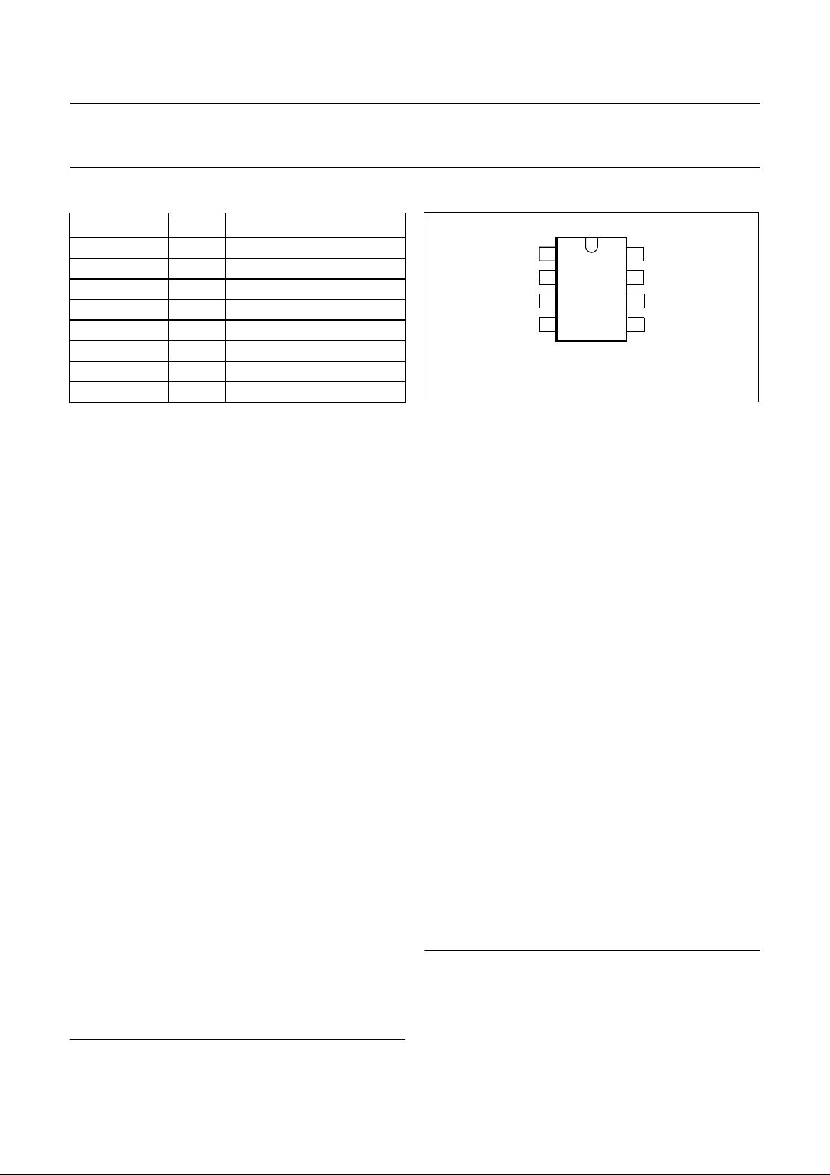
PINNING
SYMBOL PIN DESCRIPTION
V
SS
TEST 2 test output
OSC IN 3 oscillator input
OSC OUT 4 oscillator output
V
DD
M1 6 motor 1 output
M2 7 motor 2 output
RESET 8 reset input
1 ground (0 V)
5 positive supply voltage
V
SS
TEST
OSC IN
OSC OUT
1
2
PCA16xxT
3
4
MSA973
8
7
6
5
RESET
M2
M1
V
DD
Fig.1 Pin configuration, PCA16xxT, (PMFP8).
FUNCTIONAL DESCRIPTION AND TESTING
Motor pulse
The motor pulse width (t
) and the cycle times (tT) are
P
given in Chapter “Available types”.
Voltage level detector
The supply voltage is compared with the internal voltage
reference V
LIT
and V
every minute. The first voltage
EOL
level detection is carried out 30 ms after a RESET.
Lithium mode
If a lithium voltage is detected (V
DD
≥ V
), the circuit will
LIT
operate in the lithium mode. The motor pulse will be
produced with a 75% duty factor.
Silver-oxide mode
If the voltage level detected is between V
LIT
and V
EOL
, the
circuit will operate in silver-oxide mode.
Battery end-of-life
If the battery end-of-life is detected (VDD≤ V
(1)
EOL
), the
motor pulse will be produced without chopping. To indicate
this condition, bursts of 4 pulses are produced every 4 s.
Power-on reset
For correct operation of the Power-on reset the rise time of
V
from 0 V to 2.1 V should be less than 0.1 ms.
DD
All resettable flip-flops are reset. Additionally the polarity of
the first motor pulse is positive: VM1− VM2≥ 0V.
Customer testing
An output frequency of 32 Hz is provided at RESET (pin 8)
to be used for exact frequency measurement. Every
minute a jitter occurs as a result of time calibration, which
occurs 90 to 150 ms after disconnecting the RESET from
VDD.
Connecting the RESET to VDD stops the motor pulses
leaving them in a HIGH impedance 3-state condition and a
32 Hz signal without jitter is produced at the TEST pin.
A debounce circuit protects accidental stoppages due to
mechanical shock to the watch (t
= 14.7 to 123.2 ms).
DEB
Connecting RESET to VSS activates Tests 1 and 2 and
disables the time calibration.
Test 1, VDD>V
. Normal function takes place except
EOL
the voltage detection cycle (tV) is 125 ms and the cycle
time tT1 is 31.25 ms. At pin TEST a minute signal is
available at 8192 times its normal frequency.
(2)
Test 2
, VDD<V
. The voltage detection cycle (tV) is
EOL
31.25 ms and the motor pulse period (tT2) = 31.25 ms.
Test and reset mode are terminated by disconnecting the
RESET pin.
Test 3, VDD> 5.1 V. Motor pulses with a time period of
tT3= 31.25 ms and n × 122 µs are produced to check the
contents of the EEPROM. At pin TEST the motor pulse
period signal (tT) is available at 1024 times its normal
frequency. The circuit returns to normal operation when
VDD< 2.5 V between two motor pulses.
(2) Only applicable for types with the battery end-of-life detector.
(1) Only available for types with a 1 s motor pulse.
1997 Dec 12 3
Philips Semiconductors Product specification
32 kHz watch circuits with EEPROM PCA16xx series
Time calibration
Taking a normal quartz crystal with frequency 32768kHz,
frequency deviation (∆f/f) of ±15 × 10−6 and CL= 8.2 pF;
the oscillator frequency is offset (by using non-symmetrical
internal oscillator input and output capacitances of 10 pF
and 15 pF) such that the frequency deviation is
positive-only. This positive deviation can then be
compensated for to maintain time-keeping accuracy.
Once the positive frequency deviation is measured, a
corresponding number ‘n’ (see Table 1) is programmed
into the device’s EEPROM. This causes n pulses of
frequency 8192 Hz to be inhibited every minute of
operation, which achieves the required calibration.
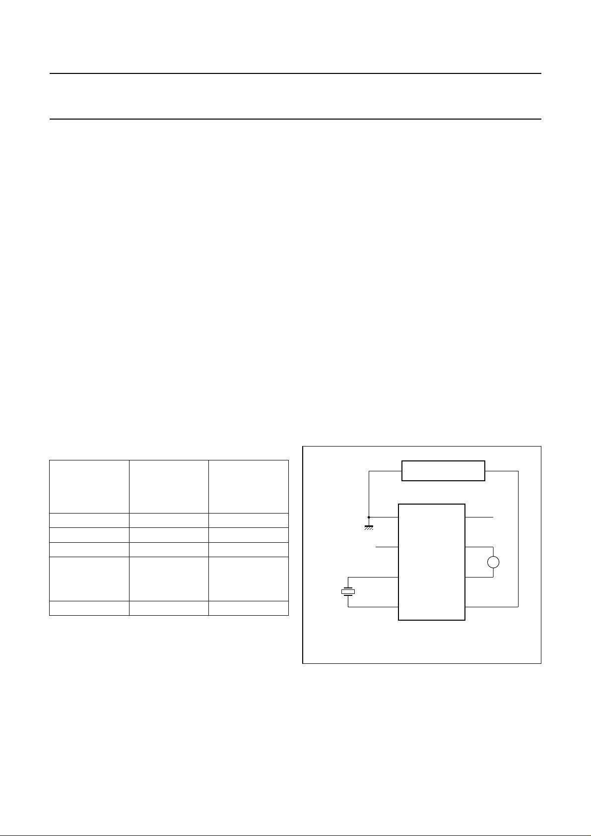
The programming circuit is shown in Fig.2. The required
number n is programmed into EEPROM by varying V
DD
according to the steps shown in Fig.3, which are
explained below:
1. The positive quartz frequency deviation (∆f/f) is
measured, and the corresponding values of n are
found according to Table 1.
2. VDD is increased to 5.1 V allowing the contents of the
EEPROM to be checked from the motor pulse period
tT3 at nominal frequency.
3. V
is decreased to 2.5 V during a motor pulse to
DD
initialize a storing sequence.
4. The first VDD pulse to 5.1 V erases the contents of
EEPROM.
5. When the EEPROM is erased a logic 1 is at the TEST
pin.
6. VDD is increased to 5.1 V to read the data by pulsing
VDD n times to 4.5 V. After the n edge, VDD is
decreased to 2.5 V.
7. VDD is increased to 5.1 V to store n bits in the
EEPROM.
8. VDD is decreased to 2.5 V to terminate the storing
sequence and to return to operating mode.
9. VDD is increased to 5.1 V to check writing from the
motor pulse period tT3.
10. VDD is decreased to the operation voltage between
two motor pulses to return to operating mode.
(Decreasing VDD during the motor pulse would restart
the programming mode).
The time calibration can be reprogrammed up to 100
times.
Table 1 Quartz crystal frequency deviation, n and t
FREQUENCY
DEVIATION
∆f/f
−6
(× 10
)
(1)
0
NUMBER OF
PULSES
(n)
0 31.250
t
T3
(ms)
+2.03 1 31.372
+4.06 2 31.494
...
...
...
+127.89 63 38.936
Notes
1. Increments of 2.03 × 10⁻⁶/step.
2. Increments of 122 µs/step.
(2)
T3
SIGNAL GENERATOR
32 kHz
V
SS
TEST
OSC IN
OSC OUT
1
2
PCA16xx
SERIES
3
4
8
7
6
5
RESET
M2
M1
V
DD
M
MSA975
Fig.2 Circuit for programming the time calibration.
1997 Dec 12 4
Philips Semiconductors Product specification
32 kHz watch circuits with EEPROM PCA16xx series
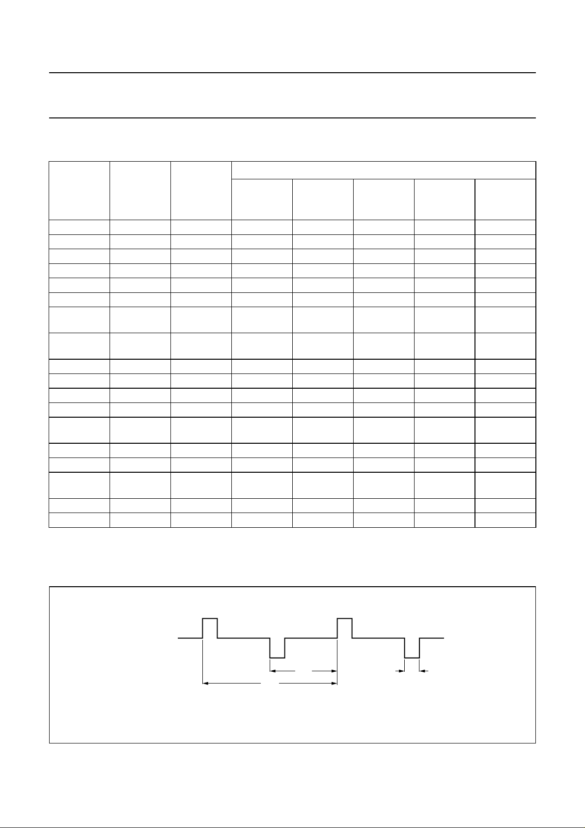
MSA948
T3
t
CHECKING
STORINGDATA INPUTERASURECONTENT CHECKING
123 n
DDP
∆ V
9 10
edge
t = 1 µs
min.
0.1 ms
S
t = 5 ms
for programming.
DD
Fig.3 V
E
t = 5 ms
3 4 5 6 7 8 9 10
4.5
5.1
DD
I
V (V)
1997 Dec 12 5
DD
2.5
(1) (1) (1) (1)
1 2
1.5
SS
0 (V )
(1) Rise and fall time should be greater than 400 µs/V for immediately correct checking.
Philips Semiconductors Product specification
32 kHz watch circuits with EEPROM PCA16xx series
AVAILABLE TYPES
Refer to Fig.4 and to Chapters “Ordering information” and “Functional description and testing”.
SPECIFICATIONS
(1)
PERIOD
t
T
(s)
PULSE
WIDTH t
(ms)
P
DRIVE
(%)
EEPROM
BATTERY
DETECTION
SHORT
TYPE
NUMBER
DELIVERY
FORMAT
1601 U/10 1 7.8 100 yes no
1602 T 1 7.8 75 yes no
1603 U/7 20 7.8 100 yes no
1604 U/10 5 7.8 75 yes no
1605 U/7 5 4.8 75 yes no
1606 U/10 10 6.8 100 yes no
1607 U 5 5.8 100
yes no 1.5 V and
75
1608 U 5 7.8 100
yes no 1.5 V and
75
161 1 U 1 6.8 75 yes no
1621 U/7 20 4.8 100 yes no
1622 U 1 4.8 100 yes yes
1623 U 20 4.8 75 yes no
1624 U 12 3.9 75
yes no 1.5 V and
56
1625 U/7 5 5.8 75 yes no
1626 U 20 5.8 100 yes no
1627 U/7 20 5.8 100
yes no 1.5 V and
75
1628 U 20 5.8 75 yes no
1629 U/7 5 6.8 75 yes no
EOL
REMARKS
2.1 V Lithium
2.1 V Lithium
2.1 V Lithium
2.1 V Lithium
Note
1. U = Chip in trays; U/7 = chip with bumps on tape; U/10 = chip on foil.
T = SOT144-1.
V
M1 - M2
t
T
2t
T
Fig.4 Motor output waveform (normal operation).
1997 Dec 12 6
MSA977
t
P
Philips Semiconductors Product specification
32 kHz watch circuits with EEPROM PCA16xx series
LIMITING VALUES
In accordance with the Absolute Maximum Rating System (IEC134).
SYMBOL PARAMETER CONDITIONS MIN. MAX. UNIT
V
DD
V
I
T
amb
T
stg
Note
1. Connecting the battery with reversed polarity does not destroy the circuit, but in this condition a large current flows,
which will rapidly discharge the battery.
HANDLING
Inputs and outputs are protected against electrostatic discharges in normal handling. However, to be totally safe, it is
advisable to take handling precautions appropriate to handling MOS devices. Advice can be found in
“Data Handbook IC16, General, Handling MOS Devices”
supply voltage VSS= 0 V; note 1 −1.8 +6 V
all input voltages V
SS
V
DD
V
output short-circuit duration indefinite
operating ambient temperature −10 +60 °C
storage temperature −30 +100 °C
.
CHARACTERISTICS
= 1.55 V; VSS=0V; f
V
DD
C
= 1 to 3 pF; unless otherwise specified.
0
= 32.768 kHz; T
osc
=25°C; crystal: RS=20kΩ; C1= 2 to 3 fF; CL= 8 to 10 pF;
amb
Immunity against parasitic impedance = 20 MΩ from one pin to an adjacent pin.
SYMBOL PARAMETER CONDITIONS MIN. TYP. MAX. UNIT
Supply
V
∆V
V
∆V
I
DD1
I
DD2
DD
DD
DDP
DDP
supply voltage T
supply voltage variation transient; VDD= 1.2 to 2.5 V −−0.25 V
supply voltage pulse programming 5.0 5.1 5.2 V
supply voltage pulse variation programming 0.55 0.6 0.65 V
supply current between motor pulses − 170 260 nA
supply current between motor pulses;
= −10 to +60 °C 1.2 1.5 2.5 V
amb
− 190 300 nA
VDD= 2.1 V
I
DD3
I
DD4
supply current stop mode; pin 8 connected to
V
DD
supply current stop mode; pin 8 connected to
− 180 280 nA
− 220 360 nA
VDD; VDD= 2.1 V
I
DD5
supply current VDD= 2.1 V;
T
= −10 to +60 °C
amb
−−600 nA
1997 Dec 12 7

Philips Semiconductors Product specification
32 kHz watch circuits with EEPROM PCA16xx series
SYMBOL PARAMETER CONDITIONS MIN. TYP. MAX. UNIT
Motor output
V
sat
R
sc
t
T
t
P
saturation voltage Σ (P + N) RL=2kΩ; T
short-circuit resistance Σ (P + N) I
transistor
<1mA − 200 300 Ω
cycle time note 1
pulse width note 2
Oscillator
V
OSC ST
g
m
t
osc
∆f/f frequency stability ∆V
C
i
C
o
starting voltage 1.2 −−V
transconductance V
≤ 50 mV 6 15 −µS
i(p-p)
start-up time − 1 − s
= 100 mV − 0.05 ×
DD
input capacitance 8 10 12 pF
output capacitance 12 15 18 pF
Voltage level detector
V
V
∆V
TC
t
V
LIT
EOL
VLD
VLD
threshold voltage lithium mode 1.65 1.80 1.95 V
threshold voltage battery end-of-life 1.27 1.38 1.46 V
hysteresis of threshold − 10 − mV
temperature coefficient −−1−mV/K
voltage detection cycle − 60 − s
Reset input
f
o
∆V
o
t
edge
I
im
I
i(av)
output frequency − 32 − Hz
output voltage swing R = 1 MΩ; C=10pF 1.4 −−V
edge time R = 1 MΩ; C=10pF − 1 −µs
peak input current note 3 − 320 − nA
average input current − 10 − nA
Test mode
cycle time for motor pulses in:
t
T1
t
T2
t
T3
t
DEB
test 1 − 125 − ms
test 2 − 31.25 − ms
test 3 see Chapter “Available types”
debounce time RESET = V
Battery end-of-life
t
EOL
t
E1
t
E2
end-of-life sequence − 4 − s
motor pulse width see “Available types” − t
time between pulses − 31.25 − ms
Notes
1. Cycle time can be changed to one of the following values: 1, 5, 10, 12 or 20 s (see Chapter “Available types”).
2. Pulse width can be varied from 2 ms to 15.7 ms in steps of 1 ms (see Chapter “Available types”).
3. Duty factor is 1 : 32 and RESET = VDDor VSS.
= −10 to +60 °C − 150 200 mV
amb
0.3 ×
−6
DD
10
14.7 − 123.2 ms
P
10
− ms
−6
1997 Dec 12 8

Philips Semiconductors Product specification
32 kHz watch circuits with EEPROM PCA16xx series
CHIP DIMENSIONS AND BONDING PAD LOCATIONS
1.44 mm
Chip area: 2.91 mm2.
Bonding pad dimensions: 110 µm× 110 µm.
Chip thickness: 200 ±25 µm, with bumps: 270 ±25 µm.
Fig.5 Bonding pad locations, PCA16xxU series, 8 terminals.
y
PCA16xxU
SERIES
0
0
V
DD
M1 M2 RESET
2.02 mm
V
SSTESTOSC INOSC OUT
x
MSA976
Table 2 Bonding pad locations (dimensions in µm)
All x/y coordinates are referenced to the centre of pad (V
), see Fig.5.
DD
PAD x y
V
SS
1290 1100
TEST 940 1100
OSC IN 481 1100
OSC OUT −102 1100
V
DD
00
M1 578 0
M2 930 0
RESET 1290 0
chip corner (max. value) −497.5 −170
1997 Dec 12 9

Philips Semiconductors Product specification
32 kHz watch circuits with EEPROM PCA16xx series
APPLICATION INFORMATION
1.55 V
V
SS
1
TEST
2
(1)
OSC IN
OSC OUT
(1) Quartz crystal case should be connected to VDD. Stray capacitance and leakage resistance from RESET, M1 or M2 to OSC IN should be less than
0.5 pF or larger than 20 MΩ.
PCA16xx
SERIES
3
4
8
7
6
5
RESET
M2
M1
V
DD
M
MSA974
Fig.6 Typical application circuit diagram.
1997 Dec 12 10
Philips Semiconductors Product specification
32 kHz watch circuits with EEPROM PCA16xx series
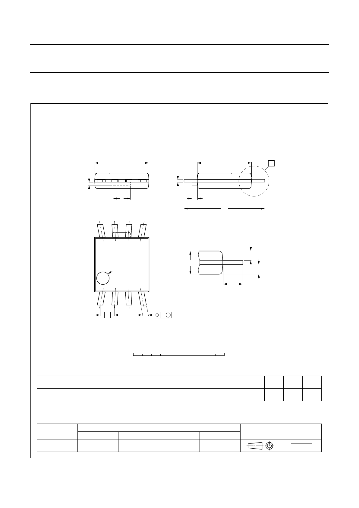
PACKAGE OUTLINE
PMFP8: plastic micro flat package; 8 leads (straight)
D
m
t n
58
pin 1 index
SOT144-1
E
c
H
E
Q
2
A
2
X
Q
1
41
e
0 2.5 5 mm
DIMENSIONS (mm are the original dimensions)
E
(1)(1)
3.1
2.9
0.90
0.70
OUTLINE
VERSION
SOT144-1
A
b
2
0.40
0.25
0.19
0.12
IEC JEDEC EIAJ
D
3.1
2.9
UNIT ce
mm
Note
1. Plastic or metal protrusions of 0.15 mm maximum per side are not included.
w M
b
0.80
REFERENCES
scale
H
4.6
4.4
L
E
0.75
m
max.
0.26
L
detail X
n
max.
0.3
Q
1
0.40
0.30
EUROPEAN
PROJECTION
0.40
0.30
Q
2
0.95
ISSUE DATE
0.1
94-01-25
95-01-24
wt
1997 Dec 12 11

Philips Semiconductors Product specification
32 kHz watch circuits with EEPROM PCA16xx series
SOLDERING
Introduction
There is no soldering method that is ideal for all IC
packages. Wave soldering is often preferred when
through-hole and surface mounted components are mixed
on one printed-circuit board. However, wave soldering is
not always suitable for surface mounted ICs, or for
printed-circuits with high population densities. In these
situations reflow soldering is often used.
This text gives a very brief insight to a complex technology.
A more in-depth account of soldering ICs can be found in
our
“IC Package Databook”
Reflow soldering
Reflow soldering techniques are suitable for all SO
packages.
Reflow soldering requires solder paste (a suspension of
fine solder particles, flux and binding agent) to be applied
to the printed-circuit board by screen printing, stencilling or
pressure-syringe dispensing before package placement.
Several techniques exist for reflowing; for example,
thermal conduction by heated belt. Dwell times vary
between 50 and 300 seconds depending on heating
method. Typical reflow temperatures range from
215 to 250 °C.
Preheating is necessary to dry the paste and evaporate
the binding agent. Preheating duration: 45 minutes at
45 °C.
(order code 9398 652 90011).
Wave soldering
Wave soldering techniques can be used for all SO
packages if the following conditions are observed:
• A double-wave (a turbulent wave with high upward
pressure followed by a smooth laminar wave) soldering
technique should be used.
• The longitudinal axis of the package footprint must be
parallel to the solder flow.
• The package footprint must incorporate solder thieves at
the downstream end.
During placement and before soldering, the package must
be fixed with a droplet of adhesive. The adhesive can be
applied by screen printing, pin transfer or syringe
dispensing. The package can be soldered after the
adhesive is cured.
Maximum permissible solder temperature is 260 °C, and
maximum duration of package immersion in solder is
10 seconds, if cooled to less than 150 °C within
6 seconds. Typical dwell time is 4 seconds at 250 °C.
A mildly-activated flux will eliminate the need for removal
of corrosive residues in most applications.
Repairing soldered joints
Fix the component by first soldering two diagonallyopposite end leads. Use only a low voltage soldering iron
(less than 24 V) applied to the flat part of the lead. Contact
time must be limited to 10 seconds at up to 300 °C. When
using a dedicated tool, all other leads can be soldered in
one operation within 2 to 5 seconds between
270 and 320 °C.
1997 Dec 12 12

Philips Semiconductors Product specification
32 kHz watch circuits with EEPROM PCA16xx series
DEFINITIONS
Data sheet status
Objective specification This data sheet contains target or goal specifications for product development.
Preliminary specification This data sheet contains preliminary data; supplementary data may be published later.
Product specification This data sheet contains final product specifications.
Limiting values
Limiting values given are in accordance with the Absolute Maximum Rating System (IEC 134). Stress above one or
more of the limiting values may cause permanent damage to the device. These are stress ratings only and operation
of the device at these or at any other conditions above those given in the Characteristics sections of the specification
is not implied. Exposure to limiting values for extended periods may affect device reliability.
Application information
Where application information is given, it is advisory and does not form part of the specification.
LIFE SUPPORT APPLICATIONS
These products are not designed for use in life support appliances, devices, or systems where malfunction of these
products can reasonably be expected to result in personal injury. Philips customers using or selling these products for
use in such applications do so at their own risk and agree to fully indemnify Philips for any damages resulting from such
improper use or sale.
1997 Dec 12 13

Philips Semiconductors Product specification
32 kHz watch circuits with EEPROM PCA16xx series
NOTES
1997 Dec 12 14

Philips Semiconductors Product specification
32 kHz watch circuits with EEPROM PCA16xx series
NOTES
1997 Dec 12 15

Philips Semiconductors – a worldwide company
Argentina: see South America
Australia: 34 Waterloo Road, NORTH RYDE, NSW 2113,
Tel. +61 2 9805 4455, Fax. +61 2 9805 4466
Austria: Computerstr. 6, A-1101 WIEN, P.O. Box 213,
Tel. +43 1 60 101, Fax. +43 1 60 101 1210
Belarus: Hotel Minsk Business Center, Bld. 3, r. 1211, Volodarski Str. 6,
220050 MINSK, Tel. +375 172 200 733, Fax. +375 172 200 773
Belgium: see The Netherlands
Brazil: see South America
Bulgaria: Philips Bulgaria Ltd., Energoproject, 15th floor,
51 James Bourchier Blvd., 1407 SOFIA,
Tel. +359 2 689 211, Fax. +359 2 689 102
Canada: PHILIPS SEMICONDUCTORS/COMPONENTS,
Tel. +1 800 234 7381
China/Hong Kong: 501 Hong Kong Industrial Technology Centre,
72 Tat Chee Avenue, Kowloon Tong, HONG KONG,
Tel. +852 2319 7888, Fax. +852 2319 7700
Colombia: see South America
Czech Republic: see Austria
Denmark: Prags Boulevard 80, PB 1919, DK-2300 COPENHAGEN S,
Tel. +45 32 88 2636, Fax. +45 31 57 0044
Finland: Sinikalliontie 3, FIN-02630 ESPOO,
Tel. +358 9 615800, Fax. +358 9 61580920
France: 4 Rue du Port-aux-Vins, BP317, 92156 SURESNES Cedex,
Tel. +33 1 40 99 6161, Fax. +33 1 40 99 6427
Germany: Hammerbrookstraße 69, D-20097 HAMBURG,
Tel. +49 40 23 53 60, Fax. +49 40 23 536 300
Greece: No. 15, 25th March Street, GR 17778 TAVROS/ATHENS,
Tel. +30 1 4894 339/239, Fax. +30 1 4814 240
Hungary: see Austria
India: Philips INDIA Ltd, Shivsagar Estate, A Block, Dr. Annie Besant Rd.
Worli, MUMBAI 400 018, Tel. +91 22 4938 541, Fax. +91 22 4938 722
Indonesia: see Singapore
Ireland: Newstead, Clonskeagh, DUBLIN 14,
Tel. +353 1 7640 000, Fax. +353 1 7640 200
Israel: RAPAC Electronics, 7 Kehilat Saloniki St, PO Box 18053,
TEL AVIV 61180, Tel. +972 3 645 0444, Fax. +972 3 649 1007
Italy: PHILIPS SEMICONDUCTORS, Piazza IV Novembre 3,
20124 MILANO, Tel. +39 2 6752 2531, Fax. +39 2 6752 2557
Japan: Philips Bldg 13-37, Kohnan 2-chome, Minato-ku, TOKYO 108,
Tel. +81 3 3740 5130, Fax. +81 3 3740 5077
Korea: Philips House, 260-199 Itaewon-dong, Yongsan-ku, SEOUL,
Tel. +82 2 709 1412, Fax. +82 2 709 1415
Malaysia: No. 76 Jalan Universiti, 46200 PETALING JAYA, SELANGOR,
Tel. +60 3 750 5214, Fax. +60 3 757 4880
Mexico: 5900 Gateway East, Suite 200, EL PASO, TEXAS 79905,
Tel. +9-5 800 234 7381
Middle East: see Italy
Netherlands: Postbus 90050, 5600 PB EINDHOVEN, Bldg. VB,
Tel. +31 40 27 82785, Fax. +31 40 27 88399
New Zealand: 2 Wagener Place, C.P.O. Box 1041, AUCKLAND,
Tel. +64 9 849 4160, Fax. +64 9 849 7811
Norway: Box 1, Manglerud 0612, OSLO,
Tel. +47 22 74 8000, Fax. +47 22 74 8341
Philippines: Philips Semiconductors Philippines Inc.,
106 Valero St. Salcedo Village, P.O. Box 2108 MCC, MAKATI,
Metro MANILA, Tel. +63 2 816 6380, Fax. +63 2 817 3474
Poland: Ul. Lukiska 10, PL 04-123 WARSZAWA,
Tel. +48 22 612 2831, Fax. +48 22 612 2327
Portugal: see Spain
Romania: see Italy
Russia: Philips Russia, Ul. Usatcheva 35A, 119048 MOSCOW,
Tel. +7 095 755 6918, Fax. +7 095 755 6919
Singapore: Lorong 1, Toa Payoh, SINGAPORE 1231,
Tel. +65 350 2538, Fax. +65 251 6500
Slovakia: see Austria
Slovenia: see Italy
South Africa: S.A. PHILIPS Pty Ltd., 195-215 Main Road Martindale,
2092 JOHANNESBURG, P.O. Box 7430 Johannesburg 2000,
Tel. +27 11 470 5911, Fax. +27 11 470 5494
South America: Rua do Rocio 220, 5th floor, Suite 51,
04552-903 São Paulo, SÃO PAULO - SP, Brazil,
Tel. +55 11 821 2333, Fax. +55 11 829 1849
Spain: Balmes 22, 08007 BARCELONA,
Tel. +34 3 301 6312, Fax. +34 3 301 4107
Sweden: Kottbygatan 7, Akalla, S-16485 STOCKHOLM,
Tel. +46 8 632 2000, Fax. +46 8 632 2745
Switzerland: Allmendstrasse 140, CH-8027 ZÜRICH,
Tel. +41 1 488 2686, Fax. +41 1 481 7730
Taiwan: Philips Semiconductors, 6F, No. 96, Chien Kuo N. Rd., Sec. 1,
TAIPEI, Taiwan Tel. +886 2 2134 2865, Fax. +886 2 2134 2874
Thailand: PHILIPS ELECTRONICS (THAILAND) Ltd.,
209/2 Sanpavuth-Bangna Road Prakanong, BANGKOK 10260,
Tel. +66 2 745 4090, Fax. +66 2 398 0793
Turkey: Talatpasa Cad. No. 5, 80640 GÜLTEPE/ISTANBUL,
Tel. +90 212 279 2770, Fax. +90 212 282 6707
Ukraine: PHILIPS UKRAINE, 4 Patrice Lumumba str., Building B, Floor 7,
252042 KIEV, Tel. +380 44 264 2776, Fax. +380 44 268 0461
United Kingdom: Philips Semiconductors Ltd., 276 Bath Road, Hayes,
MIDDLESEX UB3 5BX, Tel. +44 181 730 5000, Fax. +44 181 754 8421
United States: 811 East Arques Avenue, SUNNYVALE, CA 94088-3409,
Tel. +1 800 234 7381
Uruguay: see South America
Vietnam: see Singapore
Yugoslavia: PHILIPS, Trg N. Pasica 5/v, 11000 BEOGRAD,
Tel. +381 11 625 344, Fax.+381 11 635 777
For all other countries apply to: Philips Semiconductors, Marketing & Sales Communications,
Building BE-p, P.O. Box 218, 5600 MD EINDHOVEN, The Netherlands, Fax. +31 40 27 24825
© Philips Electronics N.V. 1997 SCA54
All rights are reserved. Reproduction in whole or in part is prohibited without the prior written consent of the copyright owner.
The information presented in this document does not form part of any quotation or contract, is believed to be accurate and reliable and may be changed
without notice. No liability will be accepted by the publisher for any consequence of its use. Publication thereof does not convey nor imply any license
under patent- or other industrial or intellectual property rights.
Internet: http://www.semiconductors.philips.com
Printed in The Netherlands 417087/1200/03/pp16 Date of release: 1997 Dec 12 Document order number: 9397 750 03142
 Loading...