

Philips PBYR235CT, PBYR245CT Datasheet
Philips Semiconductors Product specification
Rectifier diodes PBYR245CT series
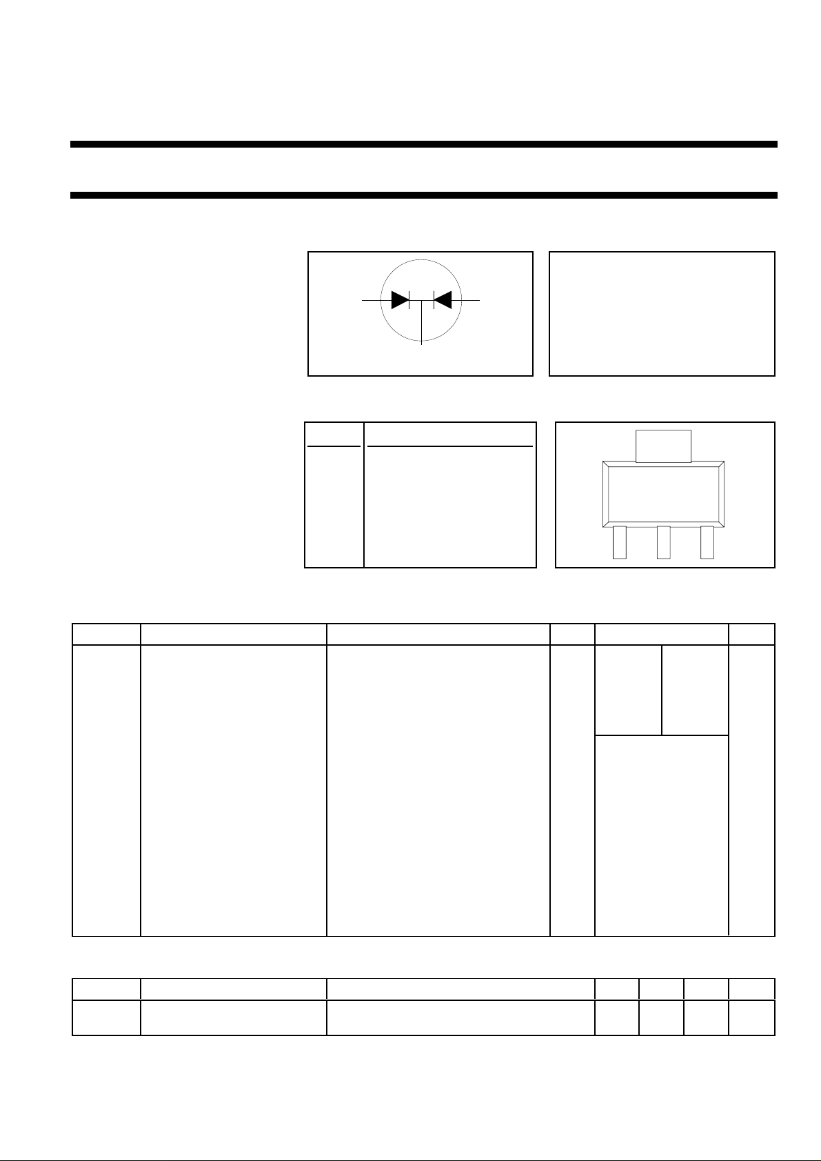
Schottky barrier
FEATURES SYMBOL QUICK REFERENCE DATA
• Low forward volt drop
• Fast switching V
• Reverse surge capability
• High thermal cycling performance I
a1
13
a2
• low profile surface mounting
k
package V
2
GENERAL DESCRIPTION PINNING SOT223
= 40 V/ 45 V
R
= 2 A
O(AV)
≤ 0.45V
F
Dual, common cathode schottky PIN DESCRIPTION
rectifier diodes in a plastic
4
envelope. Intended for use as 1 anode 1
output rectifiersin low voltage, high
frequency switched mode power 2 cathode
supplies.
3 anode 2
ThePBYR245CTseriesissupplied
in the surface mounting SOT223 tab cathode
package.
1
23
LIMITING VALUES
Limiting values in accordance with the Absolute Maximum System (IEC 134)
SYMBOL PARAMETER CONDITIONS MIN. MAX. UNIT
V
V
V
I
O(AV)
I
FRM
I
FSM
I
RRM
T
T
RRM
RWM
R
j
stg
Peak repetitive reverse - 40 45 V
voltage
Working peak reverse - 40 45 V
voltage
Continuous reverse voltage Tsp ≤ 74 ˚C - 40 45 V
Average rectified output square wave; δ = 0.5; Tsp ≤ 119 ˚C - 2 A
current (both diodes
conducting)
Repetitive peak forward square wave; δ = 0.5; Tsp ≤ 119 ˚C - 2 A
current per diode
Non-repetitive peak forward t = 10 ms - 6 A
current per diode t = 8.3 ms - 6.6 A
sinusoidal; Tj = 125 ˚C prior to
surge; with reapplied V
Peak repetitive reverse pulse width and repetition rate - 1 A
surge current per diode limited by T
Operating junction - 150 ˚C
j max
temperature
Storage temperature - 40 150 ˚C
PBYR2 40CT 45CT
RRM(max)
THERMAL RESISTANCES
SYMBOL PARAMETER CONDITIONS MIN. TYP. MAX. UNIT
R
th j-a
July 1998 1 Rev 1.400
Thermal resistance junction pcb mounted, minimum footprint - 156 - K/W
to ambient pcb mounted, pad area as in fig:1 - 70 - K/W
Philips Semiconductors Product specification
Rectifier diodes PBYR245CT series
Schottky barrier
ELECTRICAL CHARACTERISTICS
Tj = 25 ˚C unless otherwise specified
SYMBOL PARAMETER CONDITIONS MIN. TYP. MAX. UNIT
V
F
I
R
C
d
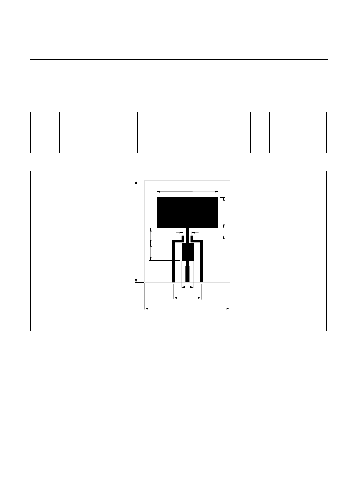
PRINTED CIRCUIT BOARD
Forward voltage IF = 1 A; Tj = 125˚C - 0.41 0.45 V
IF = 2 A - 0.58 0.7 V
Reverse current VR = V
Junction capacitance VR = 5 V; f = 1 MHz, Tj = 25˚C to 125˚C - 60 - pF
VR = V
RWM
; Tj = 100˚C - 1.5 10 mA
RWM
- 0.03 0.2 mA
Dimensions in mm.
36
18
60
4.6
9
10
7
50
15
4.5
Fig.1. PCB for thermal resistance and power rating for SOT223.
PCB: FR4 epoxy glass (1.6 mm thick), copper laminate (35 µm thick).
July 1998 2 Rev 1.400
 Loading...