


INTEGRATED CIRCUITS
USER’S MANUAL
P87C51MB2/P87C51MC2
80C51 8-bit microcontroller family with extended me mory
64KB/96KB OTP with 2KB/3KB RAM
Preliminary 2002 June 28
Version 0.95
Philips
Semiconductors

Philips Semiconductors P87C51Mx2 User Manual
P87C51Mx2Extended Address Range Micr ocontroller
1 INTRODUCTION ............................................................................................................................1
1.1 The 51MX CPU CORE ..........................................................................................................1
1.2 P87C51Mx2 microcontrollers.................................................................................................1
1.3 P87C51Mx2 Logic Symbol....................................................................................................3
1.4 P87C51Mx2 Block Diagram ..................................................................................................4
2 Memory Organization......................................................................................................................5
2.1 Programmer’s Models and Memory Maps.............................................................................5
2.2 Data Memory (DATA, IDATA, and EDATA).......................................................................6
2.2.1 Registers R0 - R7.....................................................................................................6
2.2.2 Bit Addressable RAM..............................................................................................7
2.2.3 Extended Data Memory (EDATA)..........................................................................7
2.2.4 Stack.........................................................................................................................7
2.2.5 General Purpose RAM...........................................................................................10
2.3 Special Function Registers (SFRs).......................................................................................11
2.4 External Data Memory (XDATA)........................................................................................12
2.5 High Data Memory (HDATA) .............................................................................................12
2.6 Program Memory (CODE) ...................................................................................................14
2.7 Universal Pointers.................................................................................................................15
3 51MX Instructions..........................................................................................................................20
3.1 Instruction Set Summary ......................................................................................................22
3.2 51MX Operation Code Charts..............................................................................................23
4 External Bus....................................................................................................................................28
4.1 Multiplexed External Bus.....................................................................................................28
5 Interrupt Processing.......................................................................................................................30
6 P87C51Mx2 Ports, Power Control and Peripherals....................................................................34
6.1 Special Function Registers....................................................................................................34
6.2 P87C51Mx2 Ports.................................................................................................................37
6.2.1 Ports 0, 1, 2, 3 ........................................................................................................37
6.2.2 Port 4......................................................................................................................37
6.3 P87C51Mx2 Low Power Modes...........................................................................................38
6.3.1 Stop Clock Mode ...................................................................................................38
6.3.2 Idle Mode...............................................................................................................38
6.3.3 Power-Down Mode................................................................................................38
6.3.4 Power-On Flag.......................................................................................................40
6.3.5 Design Consideration.............................................................................................40
6.3.6 ONCE™ Mode ......................................................................................................40
6.3.7 Low Power Eprom Operation (LPEP)..................................................................40
6.4 Timers/Counters 0 and 1.......................................................................................................40
6.4.1 Mode 0...................................................................................................................41
6.4.2 Mode 1...................................................................................................................41
1 Preliminary 2002 June 28

Philips Semiconductors P87C51Mx2 User Manual
P87C51Mx2Extended Address Range Micr ocontroller
6.4.3 Mode 2...................................................................................................................41
6.4.4 Mode 3...................................................................................................................42
6.5 Timer 2..................................................................................................................................44
6.5.1 Capture Mode ........................................................................................................44
6.5.2 Auto-Reload Mode (Up or Down Counter)...........................................................44
6.5.3 Programmable Clock-Out......................................................................................45
6.5.4 Baud Rate Generator Mode For UART 0 (Serial Port 0) ......................................47
6.5.5 Summary Of Baud Rate Equations........................................................................48
6.5.6 Timer/Counter 2 Set-up .........................................................................................48
6.6 UARTs..................................................................................................................................51
6.6.1 Mode 0...................................................................................................................51
6.6.2 Mode 1...................................................................................................................51
6.6.3 Mode 2...................................................................................................................51
6.6.4 Mode 3...................................................................................................................51
6.6.5 SFR and Extended SFR Spaces .............................................................................51
6.6.6 Baud Rate Generator and Selection.......................................................................52
6.6.7 Framing Error ........................................................................................................55
6.6.8 Status Register .......................................................................................................56
6.6.9 More About UART Mode 1...................................................................................57
6.6.10 More About UART Modes 2 and 3 .......................................................................58
6.6.11 Double Buffering...................................................................................................60
6.6.12 Multiprocessor Communications...........................................................................62
6.6.13 Automatic Address Recognition............................................................................62
6.7 Watchdog Timer ...................................................................................................................63
6.7.1 Watchdog Function................................................................................................63
6.7.2 Feed Sequence .......................................................................................................63
6.7.3 WDT Control.........................................................................................................66
6.7.4 WatchDog Reset Width .........................................................................................66
6.7.5 Reading from the WDCON SFR ...........................................................................66
6.7.6 Software Reset Via WatchDog Timer Feed Sequence ..........................................66
6.8 Additional Features...............................................................................................................67
6.8.1 Expanded Data RAM Addressing..........................................................................67
6.8.2 Dual Data Pointers.................................................................................................68
6.9 Programmable Counter Array (PCA) ...................................................................................68
6.9.1 PCA Capture Mode................................................................................................72
6.9.2 16-bit Software Timer Mode .................................................................................73
6.9.3 High Speed Output Mode ......................................................................................73
6.9.4 Pulse Width Modulator Mode................................................................................73
6.9.5 PCA Watchdog Timer ...........................................................................................73
2 Preliminary 2002 June 28

Philips Semiconductors P87C51Mx2 User Manual
P87C51Mx2Extended Address Range Micr ocontroller
1 INTRODUCTION
1.1 THE 51MX CPU CORE
Philips Semiconductor’s 51MX (Memory eXtension) core is based on an accelerated 80C51 architecture that executes
instructions at twice the rate of standard 80C51 devices. The linear, unsegmented address space of the 51MX core has been
expanded from the original 64 kilobytes (KB) limit to support up to 8 megabytes (MB) of program memory and 8 MB of data
memory. It retains full prog ram code compat ibility to enable design engin eers to re use 80C51 develo pment too ls, elim inating the
need to move to a new, unfamiliar architecture. The 51MX core retains 80C51 bus compatibility to allow for the continued use of
80C51-interfaced peripherals and Application-Specific Integrated Circuits (ASICs). However, by entering the Extended
Addressing Mode in order to access either data or code beyond 64 KB, the bus interface changes.
The 51MX core is completely backward compatible with the 80C51: code written for the 80C51 may be run on 51MX-based
derivatives with no changes.
Summary of differences between the classic 80C51 architecture and the 51MX core:
• Program Counter: The Program Counter is extended to 23 bits.
• Extended Data Pointer: A 23-bit Extended Data Poi nter cal le d th e EPTR h as b ee n ad ded in order to allow simp le a dju stment
to existing assembly language programs that must be expanded to address more than 64 KB of data memory.
• Stack: Two independent alte rnate Stack mo des are adde d. The first causes addresses pu shed onto the Stac k by interrupts to
be expanded to 23 bits. The second allows Stack extension into a larger memory space.
• Instruction set: A small number of instructions have extended addressing modes to allow full use of extended code and data
addressing.
• Addressing Modes: A new addre ssing mo de, Univers al Pointe r mode, is adde d that al lows acc essi ng all of the data and cod e
areas except for SFRs using a single instruction. This mode produces major improvements in size and performance of
compiled programs.
• Six clock cycles per machine cycle.
The 51MX core is described in more details in the 51MX Architecture Reference.
1.2 P87C51MX2 MICROCONTROLLERS
The P87C51Mx2 represe nts the first micr ocontroller based on the 51MX core. The P87 C51MC2 featur es 96 KB of OTP program
memory and 3 KB of data SRAM, while the P87C51MB2 has 64 KB of OTP and 2 KB of RAM. In addition, both devices are
equipped with a Programm ab le Counter Array, a watchdog timer that c an be co nfi gure d to d iffe rent time ranges, as well as two
enhanced UARTs.
The P87C51Mx2 provide s greater functionality , increased performa nce, and overall lowe r system cost. By offering an embedded
memory solution combined with the enhancements to manage the memory extension, the P87C51Mx2 eliminates the need for
software workarounds. The increased pro gram me mory enable s design eng ineers to develo p more compl ex progra ms in a highlevel language like C, for example, without struggling to contain the program within the traditional 64 KB of program memory.
These enhancements also greatly improve C language efficiency for code sizes below 64 KB.
KEY FEATURES
• 23-bit program memory space and 23-bit data memory space
• 96 KB or 64 KB of on-chip OTP
• 3 KB or 2 KB of on-chip RAM
• Up to 24 MHz CPU clock with 6 cloc k cycles per machine cycle
1 Preliminary 2002 June 28

Philips Semiconductors P87C51Mx2 User Manual
P87C51Mx2Extended Address Range Micr ocontroller
• Programmable Counter Array (PCA)
• Two full-duplex enhanced UARTs
KEY BENEFITS
• Increases program/data address range to 8 MB each
• Enhances performance and efficiency for C programs
• Fully 80C 51-compatible microcontroller
• Provides seamless and compelling upgrade path from classic 80C51
• Preserves 80C51 code base, investment/knowledge, and peripherals & ASICs
• Supported by 80C51 development and programming tools
• The P87C51Mx2 makes it possible to develop applications at a lower cost and with a reduced time-to-market
COMPLETE FEATURES
•Fully static
• Up to 24 MHz CPU clock with 6 cloc k cycles per machine cycle
• 96 KB or 64 KB of on-chip OTP
• 3 KB or 2 KB of on-chip RAM
• 23-bit program memory space and 23-bit data memory space
• Four interrupt priority levels
• 32 I/O lines (4 ports)
• Three Timers: Timer0, Timer1 and Timer2
• Two full-duplex enhanced UARTs with baud rate generator
• Framing error detection
• Automatic address recognition
• Power control modes
• Clock can be stopped and resumed
• Idle mode
• Power down mode
• Second D PTR registe r
• Asynchronous port reset
• Programmable Counter Array (PCA) (compatible with 8xC51Rx+) with five Capture/Compare modules
• Low EMI (inhibit ALE)
• Watchdog timer with programmable prescaler for different time ranges (compatible with 8xC66x with added prescaler)
80C51 COMPATIBILITY FEATURES OF THE 51MX CORE
• 100% binary compatibility with the classic 80C51 so that existing code is completely reusable
• Linear program and data address range expanded to support up to 8 MB each
• Program counter and data pointers expanded to 23 bits
• Stack pointer extended to 16 bits
2 Preliminary 2002 June 28
Philips Semiconductors P87C51Mx2 User Manual
P87C51Mx2Extended Address Range Micr ocontroller
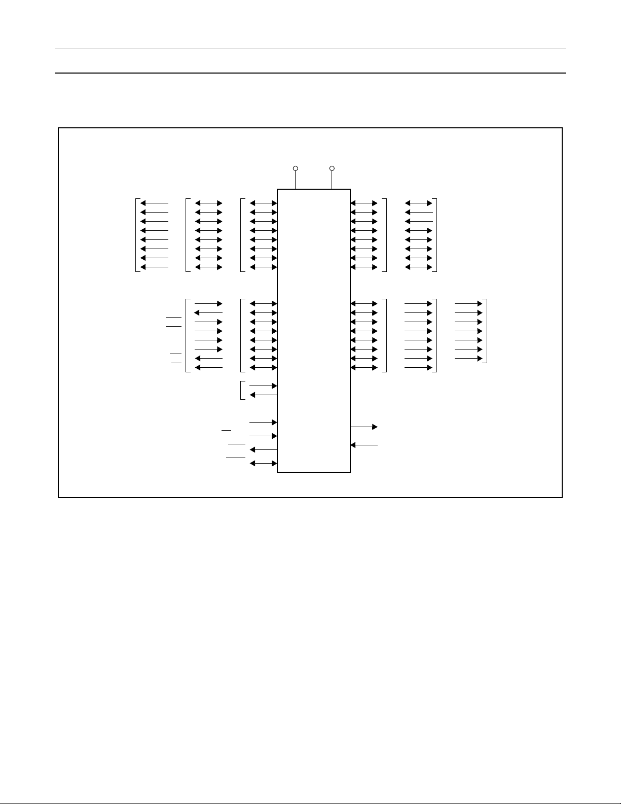
1.3 P87C51MX2 LOGIC SYMBOL
V
DD
Data Bus
PORT0
Address Bus 0-7
RXD0
TXD0
INT0
INT1
T0
T1
WR
RD
PORT3
RXD1
TXD1
RST
/Vpp
EA
PSEN
ALE/PROG
P87C51Mx2
V
SS
T2
T2EX
ECI
CEX0
PORT1
CEX1
CEX2
CEX3
CEX4
PORT2
Address Bus 8-15
XTAL2
XTAL1
Address Bus 16-22
Figure 1: P87C51Mx2 Logic Symbol
3 Preliminary 2002 June 28
Philips Semiconductors P87C51Mx2 User Manual
P87C51Mx2Extended Address Range Micr ocontroller
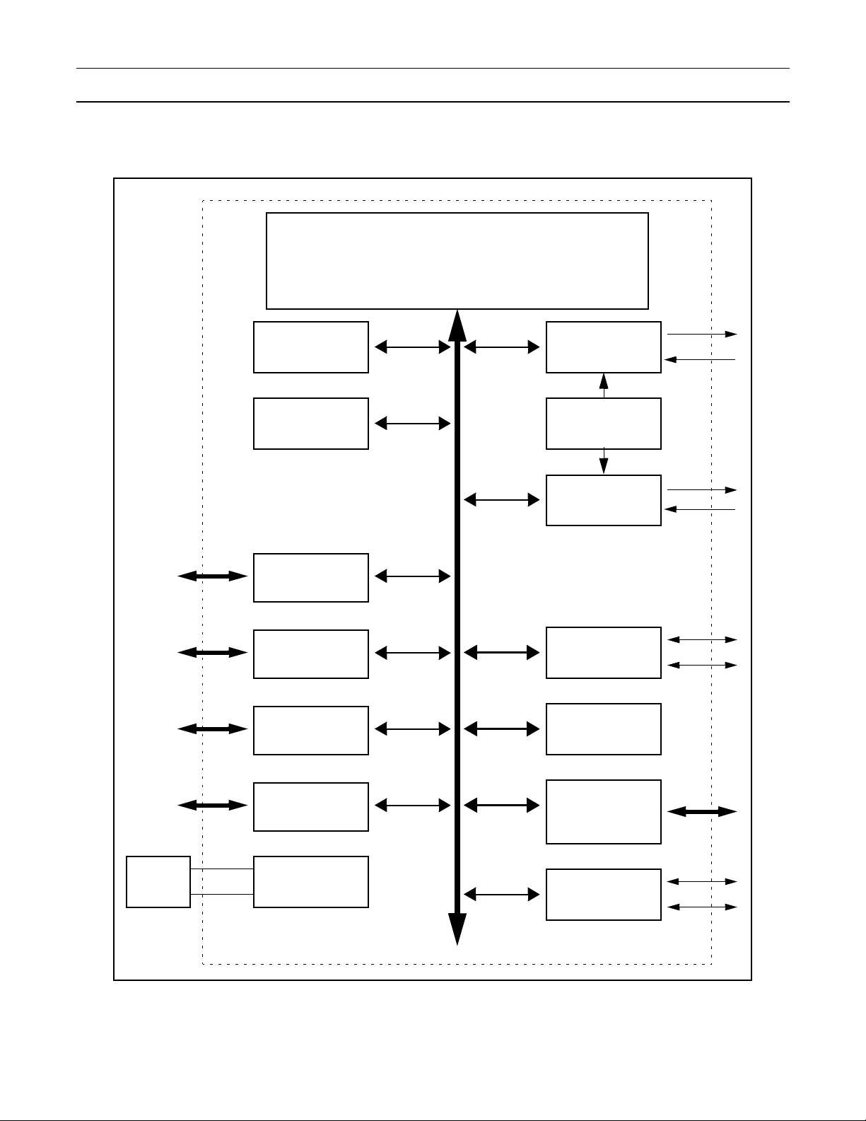
1.4 P87C51MX2 BLOCK DIAGRAM
High Performance
80C51 CPU
(51MX Core)
96KB / 64KB
Code OTP
3KB / 2KB
Data RAM
Port 3
Port 2
Port 1
UART 0
Internal Bus
Baud Rate
Generator
UART 1
Timer0
Timer1
Watchdog Timer
Crystal or
Resonator
Port 0
Oscillator
Figure 2: P87C51Mx2 Block Diagram
4 Preliminary 2002 June 28
PCA
(Programmable
Counter Array)
Timer2
Philips Semiconductors P87C51Mx2 User Manual
P87C51Mx2Extended Address Range Micr ocontroller
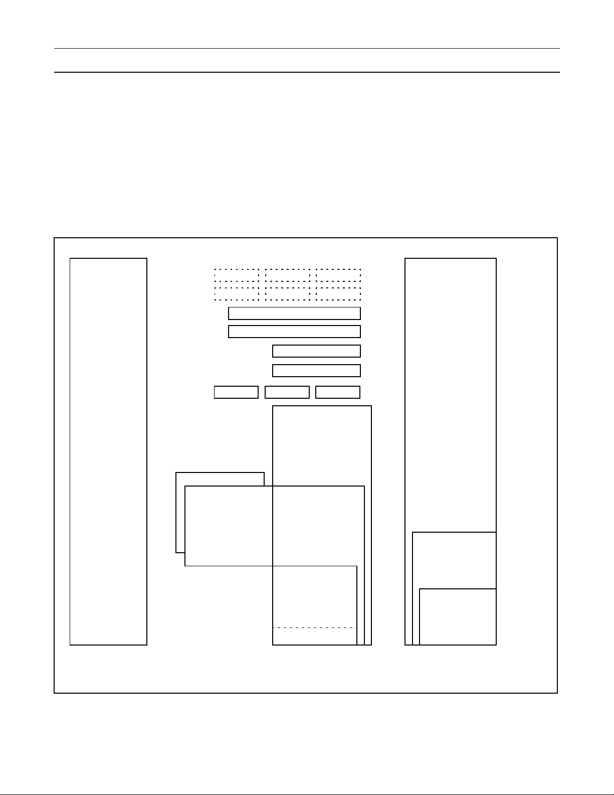
2 MEMORY ORGANIZATION
2.1 PROGRAMMER’S MODELS AND MEMORY MAPS
The P87C51Mx2 retain s all of the 80C 51 memory s paces. Additiona l memory sp ace has been a dded transpare ntly as part of the
means for allowing extended addressing. The basic memory spaces include code memory (which may be on-chip, off-chip, or
both); external data memory ; Special Function Reg isters; and inter nal data memory, whic h includes on-chip RAM, registers, and
stack. Provision is made for internal data memory to be extended, allowing a larger processor stack.
The P87C51Mx2 programmer’s model and memory map is shown in Figure 3.
CODE
On-Chip and/or
Off-Chip
Code Memory
8 MB Code
Memory Space
7F:FFFFh
00:0000h
Two 24-bit Universal Pointers
23-bit Extended Data Pointer
Extended SFRs
Special Function
Registers
(directly addressable)
R5R6R7
R1R2R3
23-bit Program Counter
Two 16-bit DPTRs
16-bit Stack Pointer
EDATA
(includes DATA & IDATA)
Extended Data
Memory
(stack and indirect
addressing)
IDATA
(includes DATA)
256 Byte On-Chip
Data Memory
(stack and indirect
addressing)
DATA
128 Byte On-Chip
Data Memory
(stack, direct and indirect
addressing)
Four Register Banks
R0 - R7
Data Memory Space
(DATA, IDATA, EDATA)
HDATA
(includes XDATA)
7E:FFFFh
ABPSW
4FFh
Off-Chip
Data Memory
100h
FFh
00:07FFh
80h
7Fh
XDATA
1792 Bytes On-Chip
Data Memory
(P87C51MC2)
XDATA
00:06FFh
00:0300h
00:02FFh
768 Bytes On-Chip
Data Memory
00h
(P87C51MB2)
00:0000h
8 MB - 64 KB External
Data Memory Space
(XDATA, HDATA)
Figure 3: P87C51MB2/C2 Programmer’s Model and Memory Map
5 Preliminary 2002 June 28

Philips Semiconductors P87C51Mx2 User Manual
P87C51Mx2Extended Address Range Micr ocontroller
Detailed descriptions of each of the various 51MX memory spaces may be found in the following summary.
DATA 128 bytes of internal data memory space (00h...7Fh) accessed via direct or indirect addressing, using instructions
other than MOVX and MOVC. All or part of the Stack may be in this area.
IDATA Indirect Data. 256 bytes of internal data memory space (00h...FFh) accessed via indirect addressing using
instructions other than MOVX and MOVC. All or part of the Stack may be in this area. This area includes the DATA
area and the 128 bytes immediately above it.
EDATA Extended Data. This is a superset of DATA and IDATA areas. Both P87C51MB2 and P87C51MC2 have 1280 bytes
of SRAM in EDATA memory. The added area may be accessed only as Stack and via indirect addressing using
Universal Pointers. The Stack may reside in the extended area if enabled to do so.
SFR Special Function Registers. Selected CPU registers and peripheral control and status registers, accessible only via
direct addressing (addresses in range 80h...FFh). This includes the new 51MX extended SFRs.
XDATA "External" Data. Duplicates the classic 80C51 64 KB memory space addressed via the MOVX instruction using the
DPTR, R0, or R1. On-chip XDATA can be disabled under program control. Also, XDATA may be placed in external
devices. P87C51MB2 has 768 bytes of on-chip XDATA memory space and P87C51MC2 has 1792 bytes of on-chip
XDATA memory space.
HDATA "High" Data. This is a superset of XDATA and may include up to 8,323,072 bytes (8 MB - 64 KB) of memory space
addressed via the MOVX instruction u s ing the EPTR, DPTR, R0, or R1. Non XDATA portion of HDATA is placed in
external devices.
CODE Up to 8 MB of Code memory, accessed as part of program execution and via the MOVC instruction.
All of these spaces except the SFR space may also be accessed through use of Universal Pointer addressing with the EMOV
instruction. This feature is detailed in a subsequent section.
2.2 DATA MEMORY (DATA, IDATA, AND EDATA)
The standard 80C51 internal data memory consists of 256 bytes of DATA/IDATA RAM, and is always entirely on-chip. In this
space are the data reg isters R 0 through R7, the de fault s tack, a bit address able RA M area, an d genera l purpos e data RAM. On
the top of the DATA/IDATA memory space is a 1 KB block of RAM that can be accessed as stack or via indirect addressing.
Alltogether this forms E DAT A RA M o f 12 80 b yte s. The different portions of the data m em ory are ac ces sed i n di fferent manners
as described in the following sections.
2.2.1 REGISTERS R0 - R7
General purpose registers R0 thro ug h R7 a ll ow q ui ck , e ffi cie nt ac ce ss to a small number of internal data m emory loc ati ons . For
example, the instruction:
MOV A,R0
uses one byte of code and executes in one machine cycle. Using direct addressing to accomplish the same result as in:
MOV A,10h
requires two bytes of code me mory and execut es in two machine cyc les. Indirect addres sing further require s setup of the pointer
register, etc.
These registers are “bank ed”. The re are fou r grou ps of reg isters, an y one of whic h may b e sele cted to re presen t R0 throug h R7
at any particular time. Th is feature m ay be used to mi nimize th e time required fo r context s witching du ring an interru pt service or
a subroutine, or to provide more register space for complicated algorithms.
The registers are no different from other internal data memory locations except that they can be addressed in "shorthand"
notation as "R0", "R1", etc. Instructions addressing the internal data memory by other means, such as direct or indirect
addressing, are quite capable of accessing the same physical locations as the registers in any of the four banks.
6 Preliminary 2002 June 28

Philips Semiconductors P87C51Mx2 User Manual
P87C51Mx2Extended Address Range Micr ocontroller
2.2.2 BIT ADDRESSABLE RAM
Internal data memory locations 20 hex through 2F hex may be accessed as both bytes and bits. This allows a convenient and
efficient way to manipulate individual flag bits without using much memory space. The bottom bit of the byte at address 20h is
bit number 00h, the next bit in the same byt e is bi t num ber 01 h, etc . The fin al bi t, bit 7 of the byte at addre ss 2Fh, is bit number
7Fh (127 decimal). Bit numbers above this refer to bits in Special Function Registers.
This code:
SETB 20h.1
CPL 20h.2
JNB 20h.2, LABEL1
sets bit 1 at address 20 hex, complements bit 2 in the same byte, then branches if the second bit is not equal to 1. In an actual
program, these bits would normally be given names and referred to by those names in the bit manipulation instructions.
2.2.3 EXTENDED DATA ME MORY (EDATA)
The 51MX architecture allows for extension of the internal data memory space beyond the traditional 256 byte limit of classic
80C51s. This space can be used as an extended or alternative processor stack space, or can be used as general purpose
storage under program control. Other than Stack Pointer based access to this space, which is automatic if Extended Stack
Memory Mode is enabled (see the following Stack section), this memory is addressed only using the new Universal Pointer
feature. Universal Pointers are described in a later section.
Both P87C51MB2 and P87C51MC2 have 1280 bytes of SRAM in EDATA memory.
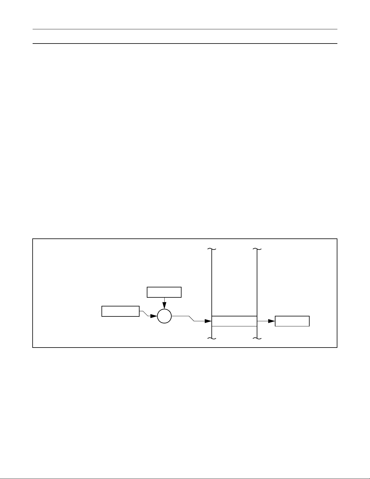
2.2.4 STACK
The processor stack pr ovide s a mean s to sto re interru pt and s ubrouti ne return a ddress es, as well as te mporar y data. Th e stac k
grows upwards, fro m lower addresse s towards higher addresses. The current Stack Poin ter always points to the last ite m pushed
on the stack, unless the stack is empty. Prior to a push operation, the Stack Pointer is incremented, then data is written to
memory. When the stack is popped, the reverse procedure is used. First, data is read from memory, then the Stack Pointer is
decremented.
The default configurat ion of the 51 MX stack is iden tical to the cl assic 80C5 1 stack imp lementati on. When inte rrupt or subrouti ne
addresses are pushed onto the stack, onl y the lower 16 bi ts of the Progra m Coun ter are stored. Thi s defaul t 80C51 mode stack
operation is shown in Figure 4.
7 Preliminary 2002 June 28
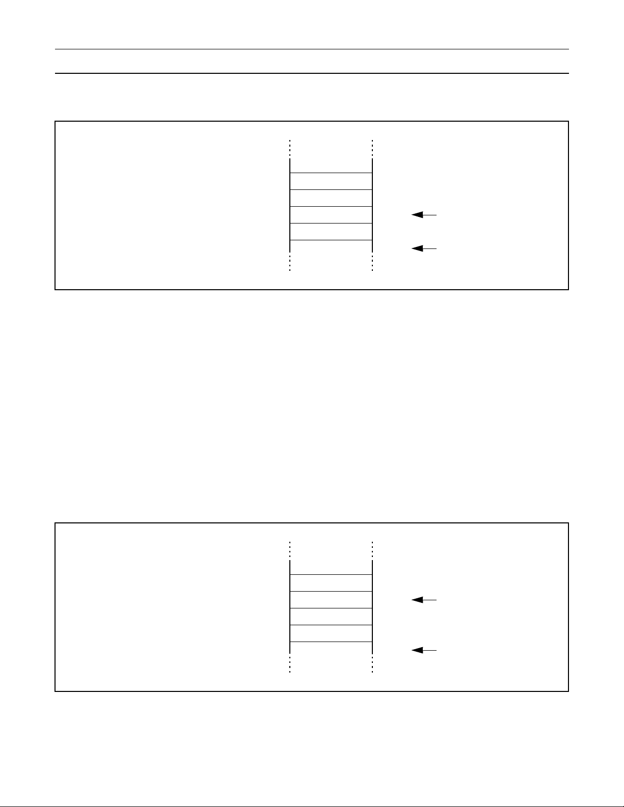
Philips Semiconductors P87C51Mx2 User Manual
P87C51Mx2Extended Address Range Micr ocontroller
0083h
0082h
Final SP Value (afte r ACALL,
LCALL or Interrupt)
Initial SP Value (before
ACALL, LCALL, or interrupt)
This figure applies to th e ACALL and
LCALL instructions in all modes. In
80C51 stack mo d e, i t al so applies to
interrupt processing.
Figure 4: Return Address Storage on the Stack (80C51 Mode)
PCH (PC.15-8)
PCL (PC.7-0)
0081h
0080h
007Fh
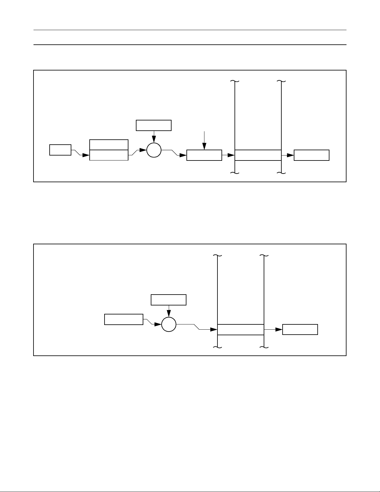
There are two configuratio n op tions fo r the stac k. For purp oses of backwa rd comp atibil ity with the class ic 80C5 1, both al ternate
modes are disabled by a c hip re set. Th e first option , Exten ded Int errupt Fra me Mo de, ca uses interru pts to p ush the e ntire 2 3-bi t
Program Counter onto the stack (as three bytes), and the RETI instruction to pop all 23-bits as a return address, as shown in
Figure 5. The upper bit of the stack byte containing the most significant byte of the Program Counter is forced to a "1" to be
consistent with Universal Pointer addressing.
Storing the full 23-bit Program Counter value is a requirement for systems that include more than 64 KB of program, since an
interrupt could occur at any point in the program. The Extended Interrupt Frame Mode changes the operation of interrupts and
the RETI instruct ion on ly, whi le oth er cal ls and returns are n ot affe cted. Sp ecial exte nded c all a nd retur n inst ruction s all ow large
programs to trave rse the entire code sp ac e w i th ful l 2 3-bi t return addresses. T he Ext end ed Interrupt Frame Mod e i s ena bl ed by
setting the EIFM bit in the MXCON register.
This figure applies to interrupt
services in Extended Interrupt Frame
Mode, as well as the ECALL
instruction in all modes.
The upper bit of the byte containing
PCE is forced to a "1" in order to be
consistent with Universal Pointers.
PCE (PC.22-16)
PCH (PC.15-8)
PCL (PC.7-0)
0083h
0082h
0081h
0080h
007Fh
Final SP Value (after
ECALL or interrupt)
Initial SP Value (before
ECALL or interrupt)
Figure 5: Extended Return Address Storage on the Stack
8 Preliminary 2002 June 28

Philips Semiconductors P87C51Mx2 User Manual
P87C51Mx2Extended Address Range Micr ocontroller
The second stack option, Extended Stack Memory Mode, allows for stack extension beyond the 256 byte limit of the classic
80C51 family. Stack extension is accomplished by increasing the Stack Pointer to 16 bits in size and allowing it to address the
entire EDATA memory rather than just the standard 256 byte internal data memory. Stack extension has no effect on the data
that is stored on the stack, it will continue to be stored as shown on in figures 4 and 5. The Extended Stack Memory Mode is
enabled by setting the ESMM bit in the MXCON register.
If the Stack Point er i s not in itia li zed b y s of tw are, the s tac k w ill be gi n a t on-chip RAM address 8, just as for the 80 C51. Als o note
that in Extended Stack Memory Mode, both MB2 and MC2 parts have 1KB of RAM on the top of DATA/IDATA space available
for the stack.
The stack mode bits ESMM and EIFM are shown in Figure 6. Note that the stack mode bits are intended to be set once during
program initialization and not altered after that point. Changing stack modes dynamically may cause stack synchronization
problems.
MXCON
Not bit addressable
Reset Value: 00h
BIT SYMBOL FUNCTION
MXCON.7 - 3 - Reserved. Programs should not write a 1 to these bits.
MXCON.2 EAM Enabl es Extended Add ressing Mod e, in connecti on with a non-volat ile user config uration
MXCON.1 ESMM Enables the Extende d Stack Me mory M ode. W hen ESMM = 0, the Stack Pointer i s 8 bit s
MXCON.0 EIFM Enables the Extended Interrupt Frame Mode. When EIFM = 0, an interrupt service will
Address: FFh (51MX Extended SFR Space)
76543210
- - - - - EAM ESMM EIFM
bit. The logical OR of the SFR bit and the non-volatile conf iguration bit deter mines whether
code and data addressing beyond 64 KB is allowed. The same logical OR value will be
read from this bit by software. When 0, all addressing (on-chip and off-chip) is limited to
64 KB each of code and data. When 1, 51MX addressing capabilities are extended
beyond boundary of 64 KB to 8 MB each of code and data, and upper address bits are
multiplexed on Port 2 for external code and/or data accesses. Refer to the External Bus
section for additional details.
EAM must be set to EAM=1 if at least one of the next two statements is true:
- there is executable code or constants in CODE space are above 64 KB
- address of data byte that has to be accessed in HDA TA is above 64 KB
in width and the sta ck is located in the IDATA m emory space. W hen ESMM = 1, th e Stack
Pointer is increased to 16-bits in width and the stack may be located anywhere in the
EDATA space. ESMM is independent of EAM and EIFM bits.
cause only the lower 16 bits of the PC to be pushed onto the stack, and an RETI
instruction will restore only the lower 16 bits of the PC. When EIFM = 1, an interrupt
service will cause all 23 bits of the PC to be pushed onto the stack, while an RETI
instruction will restore all 23 bits of the PC. EIFM must
allows execution beyond the first 64 KB of code memory.
be set to one if the application
Figure 6: MX Configuration Register (MXCON)
9 Preliminary 2002 June 28

Philips Semiconductors P87C51Mx2 User Manual
P87C51Mx2Extended Address Range Micr ocontroller
2.2.5 GENERAL P URPOSE RAM
Portions of the intern al data mem ory tha t are not used i n a parti cular a pplic ation a s registers , stac k, or bit addr essable locations
may be considered general purpose RAM and used in any desired manner.
The lower 128 bytes of the internal data memory (DATA) may be accessed using either direct or indirect addressing. Direct
addressing incorporates the entire address within the instruction. For example, the instruction:
MOV 31h,#10
will store the value 10 (decimal) in location 31 hex. Direct addresses above 128 will access the Special Function Registers rather
than the internal data memory.
Indirect addressing takes an address from either R0 or R1 of the current register bank and uses it to identify a location in the
internal data memory. The ent ire 256 byt e internal d ata memo ry space (I DATA) may be a ccessed us ing indire ct addres sing. For
example, the instruction seq uen ce :
MOV R0,#90h
MOV A,@R0
will cause the conte nts of locatio n 90 hex to be loa ded into the accum ulator. It is typ ical with the classic 80C51 to c ause the stack
to be located in the upper area, leaving more general purpose RAM in the lower area that may be accessed using both direct
and indirect add ressing. With t he 51MX, the stack may b e extended a nd moved c ompletely ou t of the low er 256 byte s of memory.
8 Bytes
7F
77
6F
67
5F
57
4F
47
3F
37
bit 7F …
2F
27
1F
17
0F
07
Figure 7: Internal Data Memory, Lower 128 Bytes
bank 3
bank 2
bank 1
bank 0
… bit 0
78
70
68
60
58
50
48
40
38
30
28
20
18
10
08
00
Undedicated
Area
Bit Addressable
Segment
Register
Banks
10 Preliminary 2002 June 28
Philips Semiconductors P87C51Mx2 User Manual
P87C51Mx2Extended Address Range Micr ocontroller
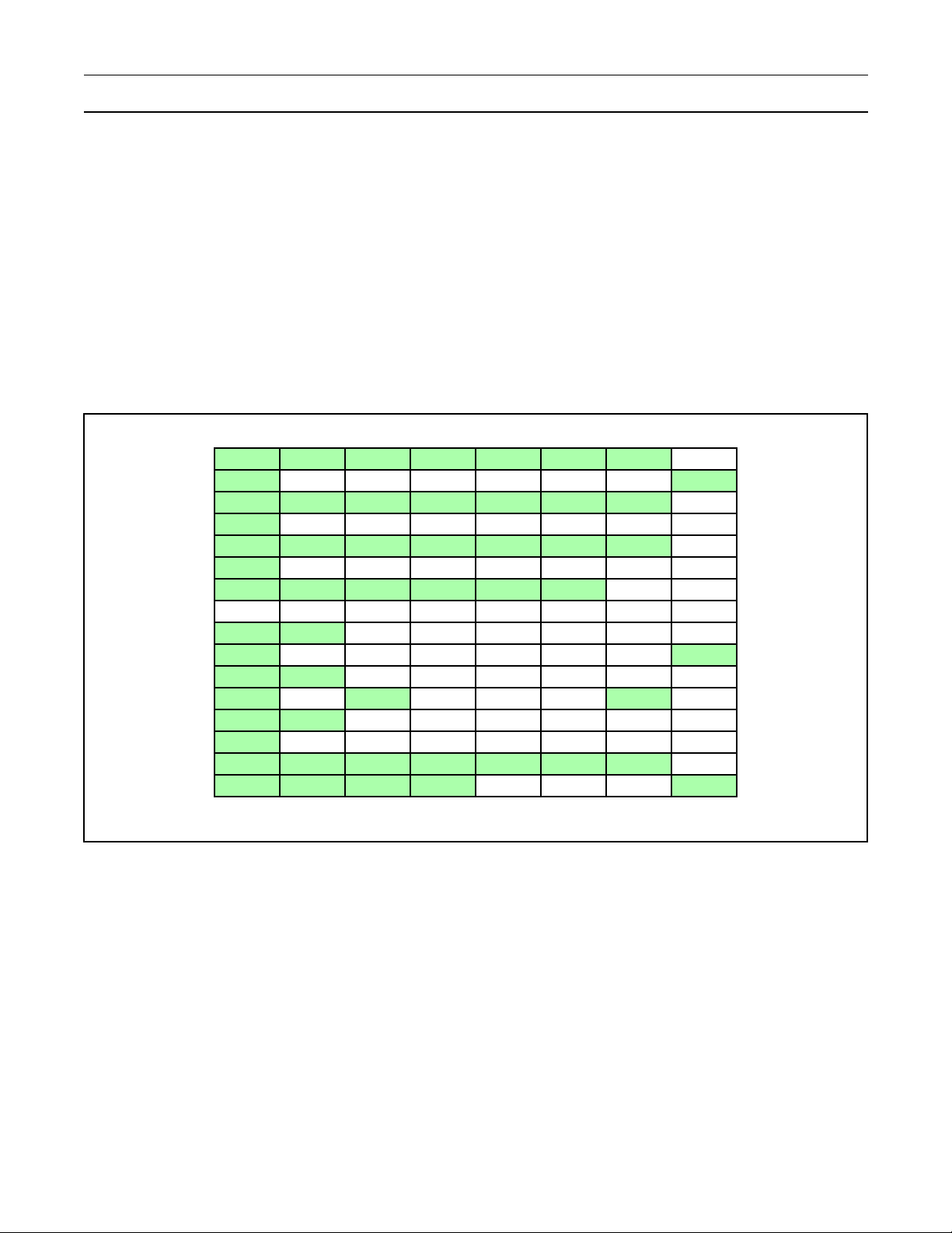
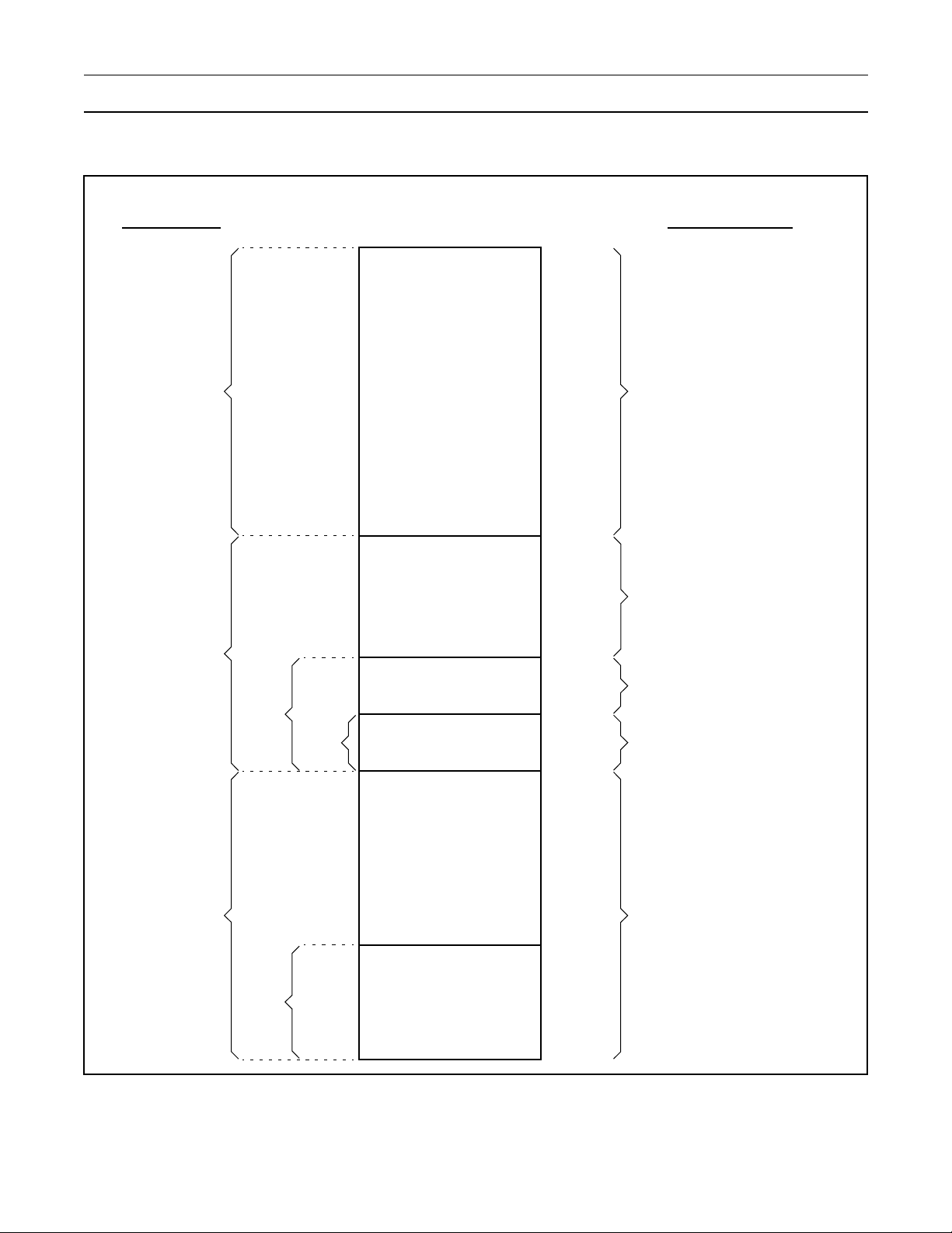
2.3 SPECIAL FUNCTION REGISTERS (SFRS)
Special Function Registers (SFRs) provide a means for the processor to access internal control registers, peripheral devices,
and I/O ports. An SFR address is always contained entirely within an instruction.
The standard SFR sp ace is 1 28 bytes in size . SFRs are i mplemen ted in each 51MX dev ice as n eeded in order to pro vide con trol
for peripherals or access to CPU features and func tions. Undefined SFR s are considered "res erved" and should not b e accessed
by user prog rams.
Sixteen addresses in the SFR space are both byte- and bit-addressable. The bit-addressable SFRs are those whose address
ends in 0h or 8h (i.e. 80h, 88h, ..., F8h). Bit addressing allows direct control and testing of bits in those SFRs.
All 51MX devices also have ad ditional 128 by tes of extended SFRs as discussed in the "51MX Architectu re Reference". Figure s
8 and 9 show the SFR and the Extended SFR maps for P87C51MB2/C2 parts.
0 / 8 1 / 9 2 / A 3 / B 4 / C 5 / D 6 / E 7 / F
F8
F0
E8
E0
D8
D0
C8
C0 C7
B8
B0
A8
A0
98
90
88
80
Bit Addressable SFRs
IP1 CH CCAP0H CCAP1H CCAP2H CCAP3H CCAP4H FF
B IP1H F7
IEN1 CL CCAP0L CCAP1L CCAP2L CCAP3L CCAP4L EF
ACC E7
CCON CMOD CCAPM0 CCAPM1 CCAPM2 CCAPM3 CCAPM4 DF
PSW D7
T2CON T2MOD R2CAPL R2CAPH TL2 TH2 CF
IP0 S0ADEN BF
P3 IP0H B7
IEN0 S0A DDR AF
P2 AUXR1 WDRST A7
S0CON S0BUF 9F
P1 97
TCON TMOD TL0 TL1 TH0 TH1 AUXR 8F
P0 SP DPL DPH PCON 87
↑
Figure 8: Standard SFR Map for the P87C51Mx2
Figure 9 shows the extended SFR map for the P87C51Mx2.
11 Preliminary 2002 June 28
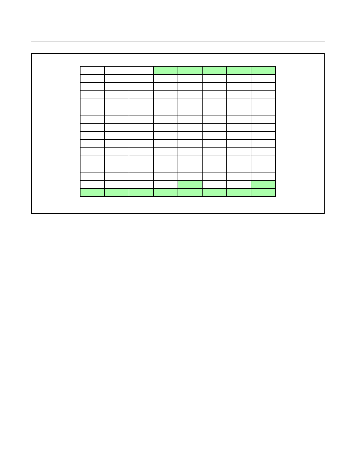
Philips Semiconductors P87C51Mx2 User Manual
P87C51Mx2Extended Address Range Micr ocontroller
0 / 8 1 / 9 2 / A 3 / B 4 / C 5 / D 6 / E 7 / F
F8
F0 F7
E8 EF
E0 E7
D8 DF
D0 D7
C8 CF
C0 C7
B8 BF
B0 B7
A8 AF
A0 A7
98 9F
90 97
88
80
S1CON S1BUF S1ADDR S1ADEN S1STAT BRGCON BRGR0 BRGR1 87
Bit Addressable SFRs
↑
SPE EPL EPM EPH MXCON FF
S0STAT WDCON 8F
Figure 9: Extended SFRs Map for the P87C51Mx2
2.4 EXTERNAL DATA MEMORY (XDATA)
The XDATA space on the 51MX is the same as the 64 KB external data memory space on the classic 80C51.
On-chip XDATA memory can be disabled under program control via the EXTRAM bit in the AUXR register. Accesses above
implemented on-chip XDATA w i ll b e rou ted to th e ex ter nal bus . If o n-c hip XDATA m em ory is dis ab led , al l XDATA a cc es ses wil l
be routed to the external bus. P87C51MB2 has 768 bytes of on-chip XDATA, while P87C51MC2 has 1792 bytes of on-chip
XDATA memory.
2.5 HIGH DATA MEMORY (HDATA)
The 51MX architecture supports up to an 8 MB data memory space, using 23-bit addressing. The entire 8 megabyte space
except for the 64 KB EDATA space is called HDATA. The XDATA space comprises the lower 64 KB of HDATA.
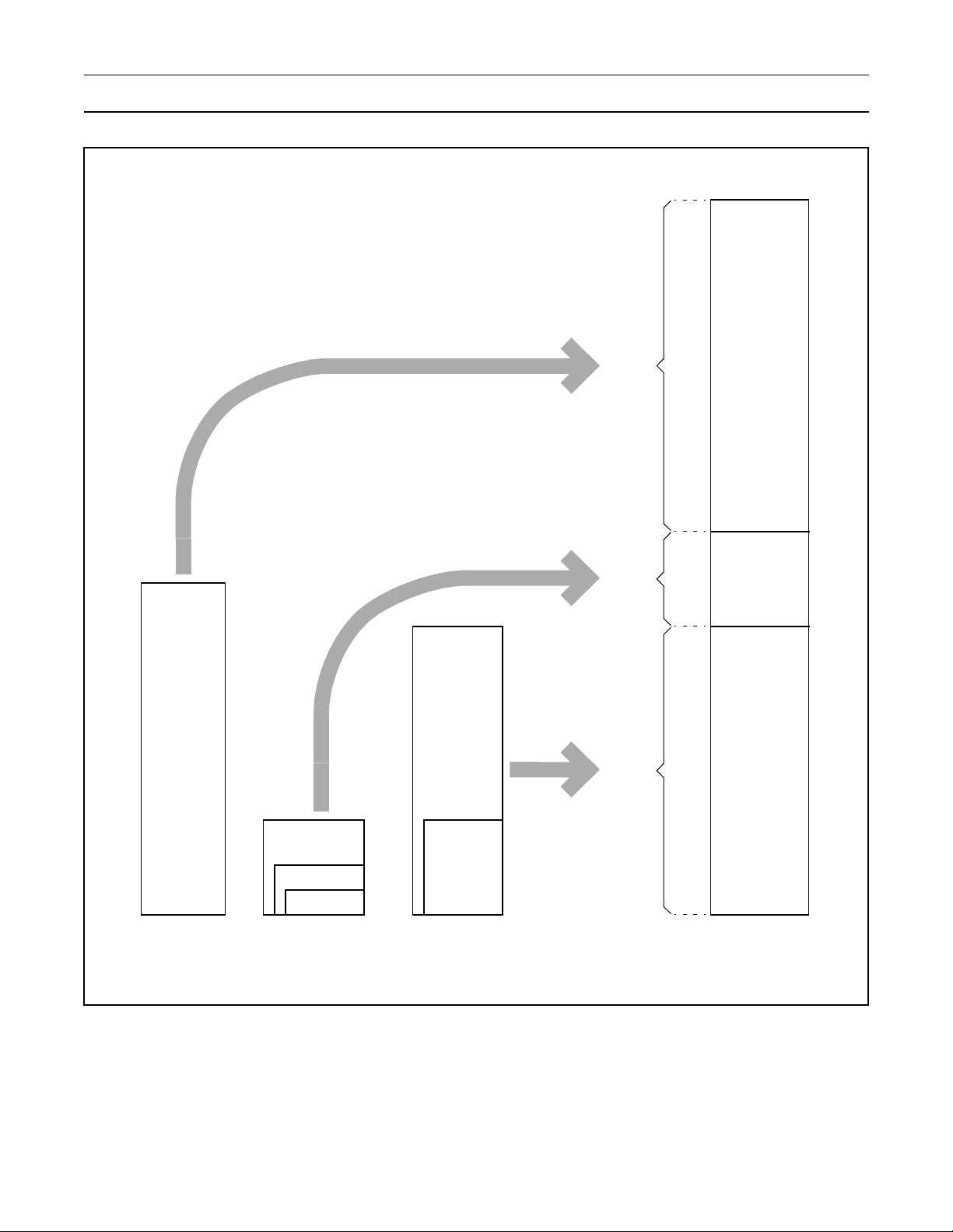
Data Pointers
The 51MX adds an addition al 23-bit Extended Data Pointer (EPTR) in order to allow a simple metho d of extending existing 80C51
programs to use mo re than 64 KB of data mem ory. If we wa nt to access a sin gle d ata by te from HDATA RAM locate d abo ve the
first 64 KB, EAM bit in MXCON sfr must be set to EAM=1.
All 80C51 instructions that use the DPTR have an 51MX variant that uses the EPTR. The 23-bit EPTR is comprised of (in order)
EPH, EPM, and EPL. Figures 10 and 11 show examples of indirect accesses to data memory using the DPTR and the EPTR
respectively. Since th e EPTR i s a 23 -bit va lue , th e 8 th b it o f EPH is not used. If read, it will ret urn a 1, like other unimplemented
bits in SFRs. Use of the EPTR allows access to the entire HDATA space, including XDATA.
12 Preliminary 2002 June 28

Philips Semiconductors P87C51Mx2 User Manual
P87C51Mx2Extended Address Range Micr ocontroller
At any point in time, one specific Data Pointer is active and is used by instructions that reference the DPTR. The active DPTR
may be changed by altering th e Data Pointer Select (DPS) bit. The DPS bit occupies the bo ttom bit of the AUXR 1 re gis ter. The
DPS bit applies only to the two DPTRs, not to the EPTR.
In the indirect addressing mode, the currently active DPTR or the EPTR provides a data memory address for accessing the
XDATA and HDATA space res pe ctive ly . Whe n th e D PTR i s used for a ddre ss in g, o nly the XDATA s pac e i s a vaila ble . Whe n th e
EPTR is used for addressing , the entire HD ATA spac e (which inc ludes the XDATA sp ace) may be ac cess ed. If the EPTR value
exceeds 7E:FFFF (the limit of HDATA), data accesses using EPTR will yield undefined results. The reason for limiting HDATA
addresses is to keep the add ressing uniform for EPTR addressing and Un iversal Pointer addres sing (which is expl ained in a later
section of this document).
Example Instruction:
MOVX @DPTR,A
Figure 10: External Data Memory Access using Indirect Addressing with DPTR
Example Instruction:
MOVX A,@EPTR
DPS
0
Data Pointers
0 = A17Ch
1 = 2962h
(00:A17Ch)
External Data
Memory
Location
00:A17Ch:
33h
External Data
Memory
Accumulator
33h
EPTR
0 = 01:1034h
Figure 11: External Data Memory Access using Indirect Addressing with EPTR
Location
01:1034h:
3Bh
Accumulator
13 Preliminary 2002 June 28
3Bh
Philips Semiconductors P87C51Mx2 User Manual
P87C51Mx2Extended Address Range Micr ocontroller
2.6 PROGRAM MEMORY (CODE)
The 80C51, and th us the 51M X, ar e "Harv ard" a rchite ctures , mea ning t hat the cod e and data space s are separ ated. I f th ere is a
single byte of executable code above 64 KB, EAM bit in MXCON sfr must be set to EAM=1. Also, if there is constant in CODE
space above 64 KB boundary that is read by the application, EAM must be set to EAM=1, too.
The 51MX expands t he 80C5 1 Program C ounter t o 23 bits , providi ng a con tiguous, unsegme nted line ar code spa ce that m ay be
as large as 8 MB. On-chip space begi ns at cod e address 0 and exten ds to the limit of the on-chip code me mory. Above th at, code
will be fetched from off-chip. The 51MX architecture allows for an external bus which supports:
• Mixed mode (some code and/or data memory off-chip).
• Single-chip operation (no external bus connection).
• ROMless operation (no use of on-chip code memory).
In some cases, c ode memory m ay be address ed as data. Exte nded instruct ion address m odes provide access to th e entire code
space of 8 MB thro ugh th e use o f inde xed i ndirect add ressing. The c urrentl y act ive DP TR, th e EP TR, a U niversa l P ointer, or the
Program Counter may be used as the base address. Examples of the various code memory addressing modes are shown in
figures 12 through 14.
Following a reset, t he 51MX begin s code execut ion like a c lassic 80C51 , at address 00:0000h. Similarly, the in terrupt vectors are
placed just above the res et addre ss, start ing at add ress 00:0 003h. I t is im portan t to not e that f irst in struct ion (located at a ddress
0) should not be an EJMP instruction. EJMP is a 5 byte instruction and would overlap any instructions intended for the external
interrupt 0 vector address.
Example Instruction:
MOVC A,@A+PC
Figure 12: Code Memory Access using Indexed Indirect Addressing with the Program Counter
PC
3E:97FFh
Accumulator
D3h
(3E:98D2h)
+
Code
Memory
Location
3E:98D2h:
70h
Accumulator
70h
14 Preliminary 2002 June 28
Philips Semiconductors P87C51Mx2 User Manual
P87C51Mx2Extended Address Range Micr ocontroller
Example Instruction:
MOVC A,@A+DPTR
executed at address 01:59B3
DPS
1
Example Instruction:
MOVC A,@A+EPTR
Data Pointers
0 = C340h
1 = FF0Ch
Figure 13: Code Memory Access using Indexe d Indir ect Addr es sing with DPTR
Accumulator
A2h
(FFAEh)
+
Upper 7 bits of
Program Counter
(01h)
01:FFAEh
01:FFAEh:
Code
Memory
Code
Memory
Location
C1h
Accumulator
C1h
Accumulator
CDh
EPTR
12:B109h
(12:B1D6h)
+
Figure 14: Code Memory Access using Indexed Indirect Addressing with EPTR
Location
12:B1D6h:
55h
Accumulator
55h
2.7 UNIVERSAL POINTERS
A new addressing mode called Universal Pointer mode has been added to the 51MX, specifically for the purpose of greatly
enhancing C langua ge code density and performance. This addressing mo de allows access to any of the on-chip or off-chip code
and data spaces usi ng one i nstruc tion, w ithou t the ne ed to kn ow in advan ce whic h of the differe nt spac es the data w ill re side in.
This includes the DATA, IDATA, EDATA, XDATA, HDATA, and CODE spaces. The SFR space is the only space that may not
be accessed using the Universal Pointer mode.
15 Preliminary 2002 June 28

Philips Semiconductors P87C51Mx2 User Manual
P87C51Mx2Extended Address Range Micr ocontroller
The Universal Pointer addressing mode uses a new set of pointer registers for two reasons. The first is that 24-bit pointers are
needed in order to allow address ing both the 8 MB code space and the 8 MB data spac e. The other reason is that it is much more
efficient to manipulate multi-byte pointer values in registers than it is in SFRs. C compilers typically already perform pointer
manipulation in registers, then move the result to a Data Pointer for use.
Two Universal Pointers are supported: PR0 and PR1. The pointer PR0 is composed of registers R1, R2, and R3 of the current
register bank, while PR1 is composed of registers R5, R6, and R7 of the current register bank, as shown in Figure 15.
PR0
MSB LSB
R3 R2 R1
Figure 15: Universal Pointer Registers
In order to access all of the various memory spaces in a single unified manner, they must all be mapped into a new "view" that
allows 16 MB of total memory space. This new view is called the Universal Memory Map.
The XDATA space is placed at th e bottom of this ne w addres s map. Th e HDATA sp ace co ntinue s abov e XDATA. The sta ndard
internal data memory space s (DATA and IDATA) are above HD ATA, followed by the remainder of the EDATA sp ace. Finally, the
code memory occupies the top of the map.
Thus, the most significant bit of the Universal Pointer determines whether code or data memory is accessed. By placing the
XDATA space at the bottom of the Universal Memory Map, Universal Pointer addresses 00:0000 through 00:FFFF can
correspond to the classic 80C5 1 ex tern al da ta m em ory spa ce . Thi s al lows for full backward compatibili ty fo r co de th at do es not
need more than 64 KB o f exte rnal da ta spac e. The Univers al Me mory M ap is shown i n Figu re 16, w hile the sta ndard v iew of th e
memory spaces and how they relate to Universal Pointer values are shown in Figure 17.
The Universal Pointers are used only by a new 51MX instruction called EMOV. The EMOV instruction allows moving data via
one of the Univers al Poin ters i nto or out of t he ac cumul ator. In eithe r case , a di splac ement of 0, 1, 2, o r 3 may als o be spec ified,
which is added to th e pointer pr ior to its use. T he displace ment allows C c ompiler acc ess of variables of up to 4 b ytes in size (e. g.
Long Integers) without the need to alter the pointer value. An example of Universal Pointer usage is shown in Figure 18. Note
that it is not possible to store a value to the CODE area of the Universal Memory Map.
MSB LSB
R7 R6 R5
PR1
Another new instruction is added to allow incrementing one of the Universal Pointers by a value from 1 to 4. This allows the
pointer to be advanced past the last data element accessed, to the next data element.
16 Preliminary 2002 June 28
Philips Semiconductors P87C51Mx2 User Manual
P87C51Mx2Extended Address Range Micr ocontroller
Memory Space Addressing Modes
FF:FFFFh
CODE
EDATA
IDATA
DATA
Up to 8 MB
on-Chip and/or off-Chip
program memory
Up to 64 KB - 256 bytes
on-chip and/or off-chip da ta
accessed as Stack and via
Universal Pointer only
Upper 128 bytes
on-chip indirectly address ed
RAM
Lower 128 bytes
on-chip directly & indirectly
addressed RAM
80:0000h
7F:FFFFh
7F:0100h
7F:00FFh
7F:0080h
7F:007Fh
7F:0000h
7E:FFFFh
PC, PC relative addressing
DPTR (lower 64 KB of Code )
EPTR
Universal Pointers: PR0, PR1
Stack (SPE / SP)
Universal Pointers: PR0, PR1
R0, R1
Stack (SPE / SP)
Universal Pointers: PR0, PR1
Direct add ressing
R0, R1 indirect
Stack (SPE / SP)
Universal Pointers: PR0, PR1
HDATA
XDATA
Up to 8 MB - 128 KB
data accessed via MOVX
(generally off-chip data)
01:0000h
00:FFFFh
Up to 64 KB
on-chip and/or off-chip
data accessed via MOVX
00:0000h
Figure 16: Universal Memory Map
17 Preliminary 2002 June 28
R0, R1 (lower 256 bytes
on-chip, lower 64 KB
off-chip via use of P2)
DPTR (XDATA access only)
EPTR (HDATA access)
Universal Pointers: PR0, PR1
Philips Semiconductors P87C51Mx2 User Manual
P87C51Mx2Extended Address Range Micr ocontroller
16MB
CODE
CODE
EDATA
IDATA
DATA
8MB
DATA,
IDATA,
EDATA
HDATA
HDATA,
XDATA
XDATA
0
24-bit Addressing using PR1 and PR2Standard Memory Map
Figure 17: Mapping of other Addressing Modes to Universal Pointer Addressing
18 Preliminary 2002 June 28

Philips Semiconductors P87C51Mx2 User Manual
P87C51Mx2Extended Address Range Micr ocontroller
Example Instruction:
EMOV @PR0+1,A
1
PR0
12:C340h
(12:C341h)
+
Figure 18: Memory Access using Universal Pointer Addressing
Universal Pointers a re desi gned prim arily to fa cilitate a ddressing in Extend ed Addressing Mode, wi th the EAM bi t in MXCON s et
to one. However, Universal Pointers may still be used when EAM = 0. In this case, Universal Pointer addressi ng can access only
the bottom 64 KB of the Code sp ace, th e 64 KB XD ATA space, a nd the 64 KB EDATA sp ace. The U niver sal Poi nter value s that
point to these areas do not change. When EAM = 0, Universal Pointer accesses outside of these areas are not accessible and
will return a value of FF hex.
Universal
Memory Map
Location
12:C341h:
39h
Accumulator
39h
19 Preliminary 2002 June 28

Philips Semiconductors P87C51Mx2 User Manual
P87C51Mx2Extended Address Range Micr ocontroller
3 51MX INSTRUCTIONS
The 51MX instruction set is a a true binary-level superset of the classic 80C51, designed to be fully compatible with previously
written 80C51 code. The changes to the instruction set are all related to the expanded address space. Some details of existing
instructions have been altered , and some instru ction s have had an extended mode added. In the la tter case, the alternate mo de
of the instruction is activated by preceding the instruction with a special one-byte prefix code, A5h.
An important goal i n t he i mp lem en tat ion of the 51MX was to ke ep the same timing relation sh ip o f ex is ti ng 8 0C 51 in structions to
existing devices. Any 80C51 instruction executed on the 51MX will take the same number of machine cycles to execute.
80C51 Instruction Effect of Extended Addressing
All relative branches
Includes SJMP and all cond itional branches . These instruct ions may cross a 64 KB bound ary if they
are located within branch range of the boundary.
ACALL addr11
AJMP addr11
JMP @A+DPTR
MOVC A,@A+DPTR
MOVC A,@A+PC
MOVX @DPTR,A The active DPTR points to an address in the 64 KB XDATA memory.
MOVX A,@DPTR The active DPTR points to an address in the 64 KB XDATA memory.
RET
RETI
LCALL addr16
This instruction wil l cross a 64 KB bo undary if it is loc ated such tha t the next inst ruction in seq uence
is across the boundary.
This instruction wil l cross a 64 KB bo undary if it is loc ated such tha t the next inst ruction in seq uence
is across the boundary.
The lower 16-bits of the Program Counter are replaced with the value formed by the sum of the
Accumulator and the active DPTR. This instruction will cro ss a 64 KB b oundary if it is loc ate d suc h
that the next instruction in sequence is across the boundary.
The address formed by replacing the lower 16-bits of the Program Counter with the value formed
by the sum of the Ac cumulato r and the active D PTR is us ed to ac cess c ode memo ry. The PC v alue
used is that of the instruction following MOVC.
The sum of the Accumula tor and the 23 -bit Progr am Counter fo rms the 23-b it address us ed to read
the code memory. The PC value used is that of the instruction following MOVC.
Replaces the lower 16 bits of the Program Counter with a 16-bit address from the Stack. This
instruction will cross a 64 KB boundary if it is located such that the next instruction in sequence is
across the boundary.
When the extended interrupt frame mode is not ena ble d, th is ins tru cti on r eplaces the lower 16 bits
of the Program Counter with a 16-bit address from the Stack. This will cause a 64 KB boundary to
be crossed if the instruction is located such that the next instruction in sequence is across the
boundary. If the extended interrupt frame mode is enabled, a 23-bit address is loaded into the PC
from the stack.
Replaces the lower 16 bi ts of the Program Counter with th e 16-bit address. This instruction will cross
a 64 KB boundary if it is located such that the next instruction in sequence is across the boundary.
LJMP addr16
Replaces the lower 16 bi ts of the Program Counter with th e 16-bit address. This instruction will cross
a 64 KB boundary if it is located such that the next instruction in sequence is across the boundary.
Table 1: Instructions Affected by Extended Address Space
20 Preliminary 2002 June 28

Philips Semiconductors P87C51Mx2 User Manual
P87C51Mx2Extended Address Range Micr ocontroller
80C51 Instruction
LCALL addr16
LJMP addr16
JMP @A+DPTR
MOVC A,@A+DPTR
MOVX @DPTR,A
MOVX A,@DPTR
INC DPTR
MOV DPTR,#data16
RET
ORL A,Rn
ANL A,Rn
XRL A,Rn
51MX Effect
Without Prefix
Load a 16-bit address into the
Program Counter.
Load a 16-bit address into the
Program Counter.
The lower 16-bits of the
Program Counter are replac ed
with the sum of the
Accumulator and the active
DPTR.
Code memory is accessed
using the address form ed by
replacing the lower 16-bits of
the Program Counter with the
sum of the Accumulator and
the active DPTR.
The active DPTR points to an
address in the 64 KB XDATA
memory.
The active DPTR points to an
address in the 64 KB XDATA
memory.
Increment the active Data
Pointer.
Load a 16-bit value into the
active Data Pointer.
Load a 16-bit address into the
Program Counter from the
Stack.
Logically OR Register n to the
Accumulator.
Logically AND Regis ter n to the
Accumulator.
Exclusive OR Reg ister n to the
Accumulator.
51MX Enhancement
(these instructions use
the prefix byte)
ECALL addr23
EJMP addr23
JMP @A+EPTR
MOVC A,@A+EPTR
MOVX @EPTR,A
MOVX A,@EPTR
INC EPTR Increment the 23 bit EPTR.
MOV EPTR,#data23 Load a 23-bit value into the EPTR.
ERET
EMOV A,@PRi+disp
EMOV @PRi+disp,A
ADD PRi,#data2
Load a 23-bit address into the Program
Counter.
Load a 23-bit address into the Program
Counter.
The Program Counter is loaded with the
value formed by th e sum of the Accumu lator
and the EPTR.
Code memory is accessed using the
address formed by the sum of the
Accumulator and the EPTR.
The EPTR points to an addre ss anywhere in
HDATA memory (not DATA, IDATA, or
EDATA).
The EPTR points to an addre ss anywhere in
HDATA memory (not DATA, IDATA, or
EDATA).
Load a 23-bit address into the Program
Counter from the Stack.
Load the Accumulator with the value from
the Universal Memory Map at the address
formed by PR0 or PR1plus the
displacement (a value fr om 0 to 3).
Load the Universal Memory Map address
formed by PR0 or PR1 plus the
displacement (a value from 0 to 3) with the
contents of the Accumulator.
Add an immediate data va lue fr om 1 to 4 to
the specified Univers al Pointer. This is a 24bit addition.
51MX Effect with Prefix
Table 2: Enhancements to the 80C51 Instruction Set Enabled by the Prefix Byte
21 Preliminary 2002 June 28

Philips Semiconductors P87C51Mx2 User Manual
P87C51Mx2Extended Address Range Micr ocontroller
3.1 INSTRUCTION SET SUMMARY
The following tabl e summarizes the entire 5 1MX instruc tion set. The instruction s are groupe d by type, and instruct ions that s hare
operand formats are combined. 51MX extended instructions and operand combinations are designated by
Data Movement Arithmetic & Logic Program Control Bit Operations
bold
text.
MOV A,Rn
XCH A,direct
A,@Ri
MOV A,#data
Rn,A
Rn,direct
Rn,#data
direct,A
direct,Rn
direct,direct
direct,@Ri
direct,#data
@Ri,A
@Ri,direct
@Ri,#data
DPTR,#data16
EPTR,#data23
MOVC A,@A+DPTR
A,@A+PC
A,@A+EPTR
MOVX A,@Ri
A,@DPTR
@Ri,A
@DPTR,A
A,@EPTR
@EPTR,A
EMOV A,@PRi+disp
@PRi+disp,A
PUSH direct
POP
ADD A,Rn
ADDC A,direct
SUBB A,@Ri
A,#data
INC A
DEC Rn
direct
@Ri
INC DPTR
EPTR
ADD PRi,#data2
MUL AB
DIV
DA A
CLR
CPL
RL
RLC
RR
RRC
SWAP
ANL A,Rn
ORL A,direct
XRL A,@Ri
A,#data
direct,A
direct,#data
JC rel
JNC
JZ
JNZ
SJMP
JB bit,rel
JNB
JBC
JMP @A+DPTR
@A+EPTR
CJNE A,direct,rel
A,#data,rel
Rn,#data,rel
@Ri,#data,rel
DJNZ Rn,rel
direct,rel
ACALL addr11
AJMP
LCALL addr16
LJMP
EJMP addr23
ECALL
RET
RETI
ERET
NOP
SETB C
CLR Bit
CPL
ANL C,bit
ORL C,/bit
MOV C,bit
bit,C
XCHD A,@Ri
Table 3: 51MX Instruction Set Summary
22 Preliminary 2002 June 28

Philips Semiconductors P87C51Mx2 User Manual
P87C51Mx2Extended Address Range Micr ocontroller
3.2 51MX OPERATION CODE CHARTS
This 51MX opcode char t consists of four page s. The first two pages are identical to a cl assic 80C51 opc ode chart exce pt that the
A5h opcode is marked as the MX extended instruction prefix value. The third and fourth pages show instruction encoding that
follows the A5h prefix. These instructions are unique to the 51MX, and are divided into several types as shown below.
Contents of Each Table Entry:
opcode bytes/cycles
instruction mnemonic
operand(s)
51MX Extended Instruction Types:
Unmodified
80C51
Instruction
New MX
Instructions
Extended
Addressing
Instructions
Extended SFR
Addressing
Operand Definitions Used in the Tables:
addr11 : 11-bit address bit : addressable bit #d8 : 8-bit immediate data
addr16 : 16-bit address dir : direct address #d16 : 16-bit immediate data
addr23 : 23-bit address rel8 : 8-bit relative address #d23 : 23-bit immediate data
These instructions are identical to classic 80C51 instructions and thus
appear only on the first two pages of the opcode chart.
These instructions are ne w to the 51MX. All are related to the Uni versal
Pointers.
These instructions incorporate extended addressing, and are modified
versions of classic 80C51 instructions.
These instructions allow access to the e xpanded SFR space. These a re
not actually new instructions, but are classic 80C51 instructions whose
function are altered by the A5h opcode.
23 Preliminary 2002 June 28

Philips Semiconductors P87C51Mx2 User Manual
P87C51Mx2Extended Address Range Micr ocontroller
00 1/1
NOP
01 2/2
AJMP
addr11
02 3/2
LJMP
addr16
03 1/1
RR
A
04 1/1
INC
A
05 2/1
INC
dir
06 1/1
INC
@R0
07 1/1
INC
@R1
08 1/1
INC
R0
09 1/1
INC
R1
0A 1/1
INC
R2
0B 1/1
INC
R3
0C 1/1
INC
R4
0D 1/1
INC
R5
0E 1/1
INC
R6
0F 1/1
INC
R7
10 3/2
JBC
bit,rel8
11 2/2
ACALL
addr11
12 3/2
LCALL
addr16
13 1/1
RRC
A
14 1/1
DEC
A
15 2/1
DEC
dir
16 1/1
DEC
@R0
17 1/1
DEC
@R1
18 1/1
DEC
R0
19 1/1
DEC
R1
1A 1/1
DEC
R2
1B 1/1
DEC
R3
1C 1/1
DEC
R4
1D 1/1
DEC
R5
1E 1/1
DEC
R6
1F 1/1
DEC
R7
20 3/2
JB
bit,rel8
21 2/2
AJMP
addr11
22 1/2
RET
23 1/1
RL
A
24 2/1
ADD
A,#d8
25 2/1
ADD
A,dir
26 1/1
ADD
A,@R0
27 1/1
ADD
A,@R1
28 1/1
ADD
A,R0
29 1/1
ADD
A,R1
2A 1/1
ADD
A,R2
2B 1/1
ADD
A,R3
2C 1/1
ADD
A,R4
2D 1/1
ADD
A,R5
2E 1/1
ADD
A,R6
2F 1/1
ADD
A,R7
30 3/2
JNB
bit,rel8
31 2/2
ACALL
addr11
32 1/2
RETI
33 1/1
RLC
A
34 2/1
ADDC
A,#d8
35 2/1
ADDC
A,dir
36 1/1
ADDC
A,@R0
37 1/1
ADDC
A,@R1
38 1/1
ADDC
A,R0
39 1/1
ADDC
A,R1
3A 1/1
ADDC
A,R2
3B 1/1
ADDC
A,R3
3C 1/1
ADDC
A,R4
3D 1/1
ADDC
A,R5
3E 1/1
ADDC
A,R6
3F 1/1
ADDC
A,R7
40 2/2
JC
rel8
41 2/2
AJMP
addr11
42 2/1
ORL
dir,A
43 3/2
ORL
dir,#d8
44 2/1
ORL
A,#d8
45 2/1
ORL
A,dir
46 1/1
ORL
A,@R0
47 1/1
ORL
A,@R1
48 1/1
ORL
A,R0
49 1/1
ORL
A,R1
4A 1/1
ORL
A,R2
4B 1/1
ORL
A,R3
4C 1/1
ORL
A,R4
4D 1/1
ORL
A,R5
4E 1/1
ORL
A,R6
4F 1/1
ORL
A,R7
50 2/2
JNC
rel8
51 2/2
ACALL
addr11
52 2/1
ANL
dir,A
53 3/2
ANL
dir,#d8
54 2/1
ANL
A,#d8
55 2/1
ANL
A,dir
56 1/1
ANL
A,@R0
57 1/1
ANL
A,@R1
58 1/1
ANL
A,R0
59 1/1
ANL
A,R1
5A 1/1
ANL
A,R2
5B 1/1
ANL
A,R3
5C 1/1
ANL
A,R4
5D 1/1
ANL
A,R5
5E 1/1
ANL
A,R6
5F 1/1
ANL
A,R7
60 2/2
JZ
rel8
61 2/2
AJMP
addr11
62 2/1
XRL
dir,A
63 3/2
XRL
dir,#d8
64 2/1
XRL
A,#d8
65 2/1
XRL
A,dir
66 1/1
XRL
A,@R0
67 1/1
XRL
A,@R1
68 1/1
XRL
A,R0
69 1/1
XRL
A,R1
6A 1/1
XRL
A,R2
6B 1/1
XRL
A,R3
6C 1/1
XRL
A,R4
6D 1/1
XRL
A,R5
6E 1/1
XRL
A,R6
6F 1/1
XRL
A,R7
70 2/2
JNZ
rel8
71 2/2
ACALL
addr11
72 2/2
ORL
C,bit
73 1/2
JMP
@A+DPTR
74 2/1
MOV
A,#d8
75 3/2
MOV
dir,#d8
76 2/1
MOV
@R0,#d8
77 2/1
MOV
@R1,#d8
78 2/1
MOV
R0,#d8
79 2/1
MOV
R1,#d8
7A 2/1
MOV
R2,#d8
7B 2/1
MOV
R3,#d8
7C 2/1
MOV
R4,#d8
7D 2/1
MOV
R5,#d8
7E 2/1
MOV
R6,#d8
7F 2/1
MOV
R7,#d8
Table 4: 51MX Operation Code Chart: Part 1
24 Preliminary 2002 June 28

Philips Semiconductors P87C51Mx2 User Manual
P87C51Mx2Extended Address Range Micr ocontroller
80 2/2
SJMP
rel8
81 2/2
AJMP
addr11
82 2/2
ANL
C,bit
83 1/2
MOVC
A,@A+PC
84 1/4
DIV
AB
85 3/2
MOV
dir,dir
86 2/2
MOV
dir,@R0
87 2/2
MOV
dir,@R1
88 2/2
MOV
dir,R0
89 2/2
MOV
dir,R1
8A 2/2
MOV
dir,R2
8B 2/2
MOV
dir,R3
8C 2/2
MOV
dir,R4
8D 2/2
MOV
dir,R5
8E 2/2
MOV
dir,R6
8F 2/2
MOV
dir,R7
90 3/2
MOV
DPTR,#d16
91 2/2
ACALL
addr11
92 2/2
MOV
bit,C
93 1/2
MOVC
A,@A+DPTR
94 2/1
SUBB
A,#d8
95 2/1
SUBB
A,dir
96 1/1
SUBB
A,@R0
97 1/1
SUBB
A,@R1
98 1/1
SUBB
A,R0
99 1/1
SUBB
A,R1
9A 1/1
SUBB
A,R2
9B 1/1
SUBB
A,R3
9C 1/1
SUBB
A,R4
9D 1/1
SUBB
A,R5
9E 1/1
SUBB
A,R6
9F 1/1
SUBB
A,R7
A0 2/2
ORL
C,/bit
A1 2/2
AJMP
addr11
A2 2/1
MOV
C,bit
A3 1/2
INC
DPTR
A4 1/4
MUL
AB
A5 -/(MX extension
prefix)
A6 2/2
MOV
@R0,dir
A7 2/2
MOV
@R1,dir
A8 2/2
MOV
R0,dir
A9 2/2
MOV
R1,dir
AA 2/2
MOV
R2,dir
AB 2/2
MOV
R3,dir
AC 2/2
MOV
R4,dir
AD 2/2
MOV
R5,dir
AE 2/2
MOV
R6,dir
AF 2/2
MOV
R7,dir
B0 2/2
ANL
C,/bit
B1 2/2
ACALL
addr11
B2 2/1
CPL
bit
B3 1/1
CPL
C
B4 3/2
CJNE
A,#d8,rel8
B5 3/2
CJNE
A,dir,rel8
B6 3/2
CJNE
@R0,#d8,rel8
B7 3/2
CJNE
@R1,#d8,rel8
B8 3/2
CJNE
R0,#d8,rel8
B9 3/2
CJNE
R1,#d8,rel8
BA 3/2
CJNE
R2,#d8,rel8
BB 3/2
CJNE
R3,#d8,rel8
BC 3/2
CJNE
R4,#d8,rel8
BD 3/2
CJNE
R5,#d8,rel8
BE 3/2
CJNE
R6,#d8,rel8
BF 3/2
CJNE
R7,#d8,rel8
C0 2/2
PUSH
dir
C1 2/2
AJMP
addr11
C2 2/1
CLR
bit
C3 1/1
CLR
C
C4 1/1
SWAP
A
C5 2/1
XCH
A,dir
C6 1/1
XCH
A,@R0
C7 1/1
XCH
A,@R1
C8 1/1
XCH
A,R0
C9 1/1
XCH
A,R1
CA 1/1
XCH
A,R2
CB 1/1
XCH
A,R3
CC 1/1
XCH
A,R4
CD 1/1
XCH
A,R5
CE 1/1
XCH
A,R6
CF 1/1
XCH
A,R7
D0 2/2
POP
dir
D1 2/2
ACALL
addr11
D2 2/1
SETB
bit
D3 1/1
SETB
C
D4 1/1
DA
A
D5 3/2
DJNZ
dir,rel8
D6 1/1
XCHD
A,@R0
D7 1/1
XCHD
A,@R1
D8 2/2
DJNZ
R0,rel8
D9 2/2
DJNZ
R1,rel8
DA 2/2
DJNZ
R2,rel8
DB 2/2
DJNZ
R3,rel8
DC 2/2
DJNZ
R4,rel8
DD 2/2
DJNZ
R5,rel8
DE 2/2
DJNZ
R6,rel8
DF 2/2
DJNZ
R7,rel8
E0 1/2
MOVX
A,@DPTR
E1 2/2
AJMP
addr11
E2 1/2
MOVX
A,@R0
E3 1/2
MOVX
A,@R1
E4 1/1
CLR
A
E5 2/1
MOV
A,dir
E6 1/1
MOV
A,@R0
E7 1/1
MOV
A,@R1
E8 1/1
MOV
A,R0
E9 1/1
MOV
A,R1
EA 1/1
MOV
A,R2
EB 1/1
MOV
A,R3
EC 1/1
MOV
A,R4
ED 1/1
MOV
A,R5
EE 1/1
MOV
A,R6
EF 1/1
MOV
A,R7
F0 1/2
MOVX
@DPTR,A
F1 2/2
ACALL
addr11
F2 1/2
MOVX
@R0,A
F3 1/2
MOVX
@R1,A
F4 1/1
CPL
A
F5 2/1
MOV
dir,A
F6 1/1
MOV
@R0,A
F7 1/1
MOV
@R1,A
F8 1/1
MOV
R0,A
F9 1/1
MOV
R1,A
FA 1/1
MOV
R2,A
FB 1/1
MOV
R3,A
FC 1/1
MOV
R4,A
FD 1/1
MOV
R5,A
FE 1/1
MOV
R6,A
FF 1/1
MOV
R7,A
Table 5: 51MX Operation Code Chart: Part 2
25 Preliminary 2002 June 28

Philips Semiconductors P87C51Mx2 User Manual
P87C51Mx2Extended Address Range Micr ocontroller
02 5/4
EJMP
addr23
05 3/2
INC
dir
10 4/3
JBC
bit,rel8
12 5/4
ECALL
addr23
15 3/2
DEC
dir
20 4/3
JB
bit,rel8
22 2/4
ERET
25 3/2
ADD
A,dir
30 4/3
JNB
bit,rel8
35 3/2
ADDC
A,dir
42 3/2
ORL
dir,A
43 4/3
ORL
dir,#d8
45 3/2
ORL
A,dir
48 2/4
EMOV
A,@PR0+0
49 2/4
EMOV
A,@PR0+1
4A 2/4
EMOV
A,@PR0+2
4B 2/4
EMOV
A,@PR0+3
4C 2/4
EMOV
A,@PR1+0
4D 2/4
EMOV
A,@PR1+1
4E 2/4
EMOV
A,@PR1+2
4F 2/4
EMOV
A,@PR1+3
52 3/2
ANL
dir,A
53 4/3
ANL
dir,#d8
55 3/2
ANL
A,dir
58 2/4
EMOV
@PR0+0,A
59 2/4
EMOV
@PR0+1,A
5A 2/4
EMOV
@PR0+2,A
5B 2/4
EMOV
@PR0+3,A
5C 2/4
EMOV
@PR1+0,A
5D 2/4
EMOV
@PR1+1,A
5E 2/4
EMOV
@PR1+2,A
5F 2/4
EMOV
@PR1+3,A
62 3/2
XRL
dir,A
63 4/3
XRL
dir,#d8
65 3/2
XRL
A,dir
68 2/4
ADD
PR0,#4
69 2/4
ADD
PR0,#1
6A 2/4
ADD
PR0,#2
6B 2/4
ADD
PR0,#3
6C 2/4
ADD
PR1,#4
6D 2/4
ADD
PR1,#1
6E 2/4
ADD
PR1,#2
6F 2/4
ADD
PR1,#3
72 3/3
ORL
C,bit
73 2/2
JMP
@A+EPTR
75 4/3
MOV
dir,#d8
Table 6: 51MX Operation Code Chart: Part 3
26 Preliminary 2002 June 28

Philips Semiconductors P87C51Mx2 User Manual
P87C51Mx2Extended Address Range Micr ocontroller
82 3/3
ANL
C,bit
85 4/3
MOV
dir,dir
86 3/3
MOV
dir,@R0
87 3/3
MOV
dir,@R1
88 3/3
MOV
dir,R0
89 3/3
MOV
dir,R1
8A 3/3
MOV
dir,R2
8B 3/3
MOV
dir,R3
8C 3/3
MOV
dir,R4
8D 3/3
MOV
dir,R5
8E 3/3
MOV
dir,R6
8F 3/3
MOV
dir,R7
90 5/4
MOV
EPTR,#d23
92 3/3
MOV
bit,C
93 2/4
MOVC
A,@A+EPTR
95 3/2
SUBB
A,dir
A0 3/3
ORL
C,/bit
A2 3/2
MOV
C,bit
A3 2/2
INC
EPTR
A6 3/3
MOV
@R0,dir
A7 3/3
MOV
@R1,dir
A8 3/3
MOV
R0,dir
A9 3/3
MOV
R1,dir
AA 3/3
MOV
R2,dir
AB 3/3
MOV
R3,dir
AC 3/3
MOV
R4,dir
AD 3/3
MOV
R5,dir
AE 3/3
MOV
R6,dir
AF 3/3
MOV
R7,dir
B0 3/3
ANL
C,/bit
B2 3/2
CPL
bit
B5 4/3
CJNE
A,dir,rel8
C0 3/3
PUSH
dir
C2 3/2
CLR
bit
C5 3/2
XCH
A,dir
D0 3/3
POP
dir
D2 3/2
SETB
bit
D5 4/3
DJNZ
dir,rel8
E0 2/4
MOVX
A,@EPTR
E5 3/2
MOV
A,dir
F0 2/4
MOVX
@EPTR,A
F5 3/2
MOV
dir,A
Table 7: 51MX Operation Code Chart: Part 4
27 Preliminary 2002 June 28

Philips Semiconductors P87C51Mx2 User Manual
P87C51Mx2Extended Address Range Micr ocontroller
4 EXTERNAL BUS
The external bus provides add res s inf ormation to external devices, and initia tes cod e read, data read , or data w rite opera tio ns.
In 51MX devices, the external bus duplicates the classic 80C51 multiplexed external bus, but allows increasing the address
output to 23 bits.
4.1 MULTIPLEXED EXTERNAL BUS
The 51MX external bus supports 8-bit data transfers and up to 23 address lines. The number of address lines available is
configurable, and depends on the setting of the EAM bit in the MXCON register.
The default for an unprogrammed part following reset is 16 address bits. This provides drop-in compatibility in existing 80C51
sockets. A non-volatile configuration bit allows pre-selecting a 23-bit address size at the time that the part is programmed.
Software may later enable the extended addressing mode even if the pre-programmed configuration does not.
The non-volatile address configuration is im ple me nte d u sin g EPR OM tec hn olo gy . Th e c onfiguration is comprised of a single bit
that enables multiplexing of the 7 extended address bits on Port 2. If the non-volatile configuration bit is not programmed,
extended addressing may be enabled at run time via the EAM bit in the MXCON SFR. Software may write a 1 to MXCON,
changing the def ault configurati on. Typically , this would be done a single time. If softwar e reads the EAM bit in MXCON, the value
will be the logical OR of the non-volatile configuration bit and the MXCON.EAM bit value. It is not recommended to change the
address configuration dynamically during program execution (for example: changing EAM=1 to EAM=0 changes external
memory bus interfac e and preve nts c ore from ex ecuti ng co de abo ve th e 64 KB bounda ry). The enco ding o f the c onfig uration bit
is such that an unprogrammed device is configured for 16 address lines.
When the full 23-bit address is multiplex ed on Port 2 (when the EAM bit in MXCON = 1), the high order addre ss informatio n (bits
A22 through A16) must be latched externally in the same manner as the low order bits (A7 through A0) on Port 0. The middle
address bits (A15 through A8 ) appe ar on Port 2 aft er ALE go es low. If ex ten ded addressing is not enabled , Port 2 b eha ve s ju st
as on a classic 80C51. An example of Port 2 address multiplexing is shown in Figure 19.
There are two special cases for Port 2 multiplexing when extended addressing is enabled: MOVX @Ri and MOVX @DPTR.
These instructions do not supply a source for a full 23-bit external address. Where program memory is involved (jumps and
MOVC), any "missing" addre ss bits are supplied by the Program Counter (se e Table 1). For MOVX, th e additional bi ts are forced
to zeroes to complete the addres s. So, MOVX @Ri will output a 23-bit add ress composed of seven zeroes for the upper address,
Port 2 SFR contents for the middle byte of the ad dress, and Ri conten ts for the bottom byte. Similarly, MOVX @DPTR will output
a 23-bit address composed of seven zeroes for the upper address and the current DPTR contents for the middle and bottom
bytes of the address.
If we have a single-chip application with code exceeding 64 KB (and thus having EAM=1) and if an old 51 bus interface has to
be preserved, instead of using MOVX @Ri,A the instruction EMOV @PRi,A should be used. If we load the content of P2 sfr to
R3 and R2, exe cutio n of i nstruc tion EMOV @ PR0 ,A will have exac tly t he sa me outpu t in a sy stem with EAM =1 as it i s in case of
MOVX @R0,A in a design with standard 51bus interface.
Some 51MX appli cations may use extended addressin g and rel y on s oftware setting t he EAM bi t in MXC ON (i.e. the non -volatile
address configuration bit is not prog ram me d). If su ch an app lic ati on is set up suc h tha t the fi rst co de exec ute d upo n res et is offchip, then the instruction that sets the EAM bit in MXCON must be located at or below address 00FBh. This is to prevent the
external bus from supplying a 16-bit address when a 23-bit address is required. If the Program Counter were to reach address
0100h while EAM = 0, the apparent address (to external hardware that is expecting a 23-bit address) would become 01:0100.
28 Preliminary 2002 June 28

Philips Semiconductors P87C51Mx2 User Manual
P87C51Mx2Extended Address Range Micr ocontroller
S1 S2 S3 S4 S5 S6 S1 S2
ALE
P2
P0
high
address
low
address
middle
address
instruction
data in
high
address
low
address
middle
address
instruction
data in
low
address
PSEN
Figure 19: Example of External Code Memory Read Cycles using 23 Address Bits
The standard control signals and their functions for the external bus are as follows:
Signal name
Function
ALE Address Latch Enable. This signal directs an external address latch to store the multiplexed portion of the
address for the next bus operation. This may be either a data address or a code address.
PSEN
Program Store Enable. Indicates that the processor is reading code from the bus. Typically connected to the
Output Enable pin of external EPROMs or other memory devices. External bus addresses for code memory
may range from 00:0000 through 7F:FFFF. In the Universal Memory Map, these correspond to addresses
80:0000 through FF:FFFF
RD
WR
Read. The external data read strobe. Typically connected to the RD pin of external peripheral devices.
Write. The write strobe for external data. Typically connected to the WR pin of external peripheral devices.
External bus addresses for data memory may range from 00:0000 through 7E:FFFF, which matches Universal Memory Map
addresses. If on-chip XDAT A is enabled , it will c ause an addres sing disco ntinuity i n the extern al data addre ss space. Th e DATA
and IDATA spaces are always on-chip, and therefore always create such an addressing discontinuity.
29 Preliminary 2002 June 28

Philips Semiconductors P87C51Mx2 User Manual
P87C51Mx2Extended Address Range Micr ocontroller
5 INTERRUPT PROCESSING
The P87C51Mx2 uses a four priority level interrupt structure. This allows great flexibility in controlling the handling of the many
interrupt sources. The P87C51Mx2 has ten interrupt sources.
Each interrupt source can be individually enabled or disabled by setting or clearing a bit in registers IEN0 or IEN1. The IEN0
register also contains a global disable bit, EA, which disables all interrupts at once.
Each interrupt source can be individually programmed to one of four priority levels by setting or clearing bits in the IP0, IP0H,
IP1, and IP1H registers. An i nterrupt service routine in prog ress can be interrupted by a higher priority interrup t, but not by another
interrupt of the same or lower priority. The highest priority interrupt service cannot be interrupted by any other interrupt source.
So, if two requests of different priority levels are received simultaneously, the request of higher priority level is serviced.
If requests of the same priority level are received simultaneously, an internal polling sequence determines which request is
serviced. This is c al led th e a r bi trati on ran ki ng. N ote th at the arb itra t io n ra nk ing i s onl y us ed to resolve simultaneo us requests of
the same priority level.
Table 8 summarize s the inte rrupt sourc es, flag bits, ve ctor addres ses, en able bits , priority bits, pol ling prior ity, and w hether each
interrupt may wake up the CPU from Power Down mode.
Description
Interrupt
Flag Bit(s)
Vector
Address
Interrupt
Enable Bit(s)
Interrupt
Priority
Polling
Priority
Power Down
Wakeup
External Interrupt 0 IE0 0003h EX0 (IEN0.0) IP0H.0, IP0.0 1 (highest) Yes
Timer 0 Interrupt TF0 000Bh ET0 (IEN0.1) IP0H.1, IP0.1 2 No
External Interrupt 1 IE1 0013h EX1 (IEN0.2) IP0H.2, IP0.2 3 Yes
Timer 1 Interrupt TF1 001Bh ET1 (IEN0.3) IP0H.3, IP0.3 4 No
Serial Port 0 Tx and Rx
Serial Port 0 Rx
1
1,5
TI_0 & RI_0
RI_0
5
0023h ES0(IEN0.4) IP0H.4, IP0.4 6 No
Timer 2 Interrupt TF2, EXF2 0 02Bh ET2 (IEN0.5) IP0H.5, IP0.5 7 No
PCA interrupt CF, CCFn* 0033h EC (IEN0.6) IP0H.6, IP0.6 5 No
Serial Port 1 Tx and Rx
Serial Port 1 Rx
Serial Port 0 Tx
Serial Port 1 Tx
2
3
4
2,6
TI_1 & RI_1
RI_1
TI_0 003Bh EI10 (IEN1.1) IP1H.1, IP1.1 8 No
TI_1 0043h EI11 (IEN1.2) IP1H.2, IP1.2 9 No
6
0053h ES1 (IEN1.0) IP1H.0, IP1.0 10 (lowest) No
1. S0STAT.5 = 0 selects combined Serial Port 0 Tx and Rx interrupt; S0ST AT.5 = 1 selec ts Serial Port 0 Rx interrupt o nly (and
TX interrupt will be different, see Note 3 below).
2. S1STAT.5 = 0 selects combined Serial Port 1 Tx and Rx interrupt; S1ST AT.5 = 1 selec ts Serial Port 1 Rx interrupt o nly (and
TX interrupt will be different, see Note 4 below).
3. This interrupt is used as Serial Port 0 Tx interrupt if and only if S0STAT.5 = 1, and is disabled otherwise.
4. This interrupt is used as Serial Port 1 Tx interrupt if and only if S1STAT.5 = 1, and is disabled otherwise.
5. If S0STAT.0 = 1, the following Serial Port 0 additional flag bits can cause this interrupt: FE_0, BR_0, OE_0.
6. If S1STAT.0 = 1, the following Serial Port 1 additional flag bits can cause this interrupt: FE_1, BR_1, OE_1.
Table 8: Summary of Interrupts
30 Preliminary 2002 June 28

Philips Semiconductors P87C51Mx2 User Manual
P87C51Mx2Extended Address Range Micr ocontroller
IEN0
Bit addressable
Reset Value: 00h
BIT SYMBOL FUNCTION
IEN0.7 EA Interrupt Enable Bit.
IEN0.6 EC PCA Interrupt Enable bit.
IEN0.5 ET2 Timer 2 Interrupt Enable.
IEN0.4 ES0/ES0R Serial Port 0 Combined Interrupt Enable (S0STAT.5 = 0)/Serial Port 0 Receive Interrupt
IEN0.3 ET1 Timer1 Overflow Interrupt Enable.
IEN0.2 EX1 External Interrupt 1 Enable.
IEN0.1 ET0 Timer 0 Overflow Interrupt Enable.
IEN0.0 EX0 External Interrupt 0 Enable.
IEN1
Bit addressable
Reset Value: 00h
Address: A8h
Address: E8h
76543210
EA EC ET2
Enable (S0STAT.5 = 1).
Figure 20: Interrupt Enable Register IEN0
76543210
- - - - - ES1T ES0T
ES0/ES0R
ET1 EX1 ET0 EX0
ES1/ES1R
BIT SYMBOL FUNCTION
IEN1.7-3 - Reserved for future use. Should be set to 0 by user programs.
IEN1.2 ES1T If S1STAT.5 = 1, it is Serial Port 1 Transmit Interrupt Enable. If S1STAT.5 = 0, this
interrupt is disabled anyway.
IEN1.1 ES0T If S0STAT.5 = 1, it is Serial Port 0 Transmit Interrupt Enable. If S0STAT.5 = 0, this
interrupt is disabled anyway.
IEN1.0 ES1/ES1R Serial Port 1 Combined Interrupt Enable (S1STAT.5 = 0)/Serial Port 1 Receive Interrupt
Enable (S1STAT.5 = 1).
Figure 21: Interrupt Enable Register IEN1
31 Preliminary 2002 June 28

Philips Semiconductors P87C51Mx2 User Manual
P87C51Mx2Extended Address Range Micr ocontroller
IP0
Bit addressable
Reset Value: 00h
BIT SYMBOL FUNCTION
IP0.7 - Reserved for future use. Should be set to 0 by user programs.
IP0.6 PPC PCA Interrupt Priority bit Low Bit.
IP0.5 PT2 Timer 2 Interrupt Priority Low Bit.
IP0.4 PS0/PS0R Serial Port 0 Combined Interrupt (S0STAT.5 = 0)/Receive Interrupt (S0STAT.5 = 1)
IP0.3 PT1 Timer 1 Interrupt Priority Low Bit.
IP0.2 PX1 External Interrupt 1 Priority Low Bit.
IP0.1 PT0 Timer 0 Interrupt Priority Low Bit.
IP0.0 PX0 External Interrupt 0 Priority Low Bit.
IP0H
Not bit addressable
Reset Value: 00h
Address: B8h
Address: B7H
76543210
- PPC PT2
Priority Low Bit.
Figure 22: Interrupt Priority Register IP0
76543210
- PPCH PT2H
PS0/PS0R
PS0H/PS0RH
PT1 PX1 PT0 PX0
PT1H PX1H PT0H PX0H
BIT SYMBOL FUNCTION
IP0H.7 - Reserved for future use. Should be set to 0 by user programs.
IP0H.6 PPCH PCA Interrupt Priority bit High Bit.
IP0H.5 PT2H Timer 2 Interrupt Priority High Bit.
IP0H.4 PS0H/PS0RH Serial Port 0 Combined Interrupt (S0STAT.5 = 0)/Receive Interrupt (S0STAT.5 = 1)
Priority High Bit.
IP0H.3 PT1H Timer 1 Interrupt Priority High Bit.
IP0H.2 PX1H External Interrupt 1 Priority High Bit.
IP0H.1 PT0H Timer 0 Interrupt Priority High Bit.
IP0H.0 PX0H External Interrupt 0 Priority High Bit.
Figure 23: Interrupt Priority High Byte IP0H
32 Preliminary 2002 June 28

Philips Semiconductors P87C51Mx2 User Manual
P87C51Mx2Extended Address Range Micr ocontroller
IP1
Bit addressable
Reset Value: 00h
BIT SYMBOL FUNCTION
IP1.7-3 - Reserved for future use. Should be set to 0 by user programs.
IP1.2 PS1T Serial Port 1 transmit Interrupt (S1STAT.5 = 1) Priority Low Bit.
IP1.1 PS0T Serial Port 0 transmit Interrupt (S0STAT.5 = 1) Priority Low Bit.
IP1.0 PS1/PS1R Serial Port 1 combined Interrupt (S1STAT.5 = 0)/receive Interrupt (S1STAT.5 = 1) Priority
IP1H
Not bit addressable
Reset Value: 00h
BIT SYMBOL FUNCTION
IP1H.7-3 - Reserved for future use. Should be set to 0 by user programs.
IP1H.2 PS1TH Serial Port 1 transmit Interrupt (S1STAT.5 = 1) Priority High Bit.
IP1H.1 PS0TH Serial Port 0 transmit Interrupt (S0STAT.5 = 1) Priority High Bit.
IP1H.0 PS1H/PS1RH Serial Port 1 combined Interrupt (S1STAT.5 = 0)/receive Interrupt (S1STAT.5 = 1) Priority
Address: F8H
Address: F7H
76543210
- - - - - PS1T PS0T
Low Bit.
Figure 24: Interrupt Priority Register 1
76543210
- - - - - PS1TH PS0TH
High Bit.
PS1/PS1R
PS1H/PS1RH
Figure 25: Interrupt Priority Register 1 High Byte
33 Preliminary 2002 June 28

Philips Semiconductors P87C51Mx2 User Manual
P87C51Mx2Extended Address Range Micr ocontroller
6 P87C51MX2 PORTS, POWER CONTROL AND
PERIPHERALS
6.1 SPECIAL FUNCTION REGISTERS
Note: Special Function Registers (SFRs) accesses are restricted in the following ways:
1. User must NOT attempt to access any SFR locations not defined.
2. Accesses to any defined SFR locations must be strictly for the functions for the SFRs.
3. SFR bits labeled ’-’, ’0’ or ’1’ can ONLY be written and read as follows:
- ’-’ MUST be written with ’0’, but can return any value when read (even if it was written with ’0’). It is a reserved bit and may
be used in future derivatives.
- ’0’ MUST be written with ’0’, and will return a ’0’ when read.
- ’1’ MUST be written with ’1’, and will return a ’1’ when read.
Special Function Registers
SYMBOL DESCRIPTION
ACC* Accumulator E0H 00H
AUXR#Auxiliary Function Register 8EH------EXTRAMAO00H
AUXR1# Auxiliary Function Register 1 A2H - - - LPEP GF2 0 - DPS 00H
B* B Register F0H 00H
BRGR0#§ Baud Rate Generator Rate Low 86H
BRGR1#§ Baud Rate Generator Rate High 87H
BRGCON# Baud Rate Generator Control 85H
CCAP0H# Module 0 Capture High FAH XXH
CCAP1H# Module 1 Capture High FBH XXH
CCAP2H# Module 2 Capture High FCH XXH
CCAP3H# Module 3 Capture High FDH XXH
CCAP4H# Module 4 Capture High FEH XXH
CCAP0L# Module 0 Capture Low EAH XXH
CCAP1L# Module 1 Capture Low EBH XXH
CCAP2L# Module 2 Capture Low ECH XXH
CCAP3L# Module 3 Capture Low EDH XXH
CCAP4L# Module 4 Capture Low EEH XXH
CCAPM0# Module 0 Mode DAH - ECOM_0 CAPP_ 0 CAPN_0 MAT_0 TOG_0 PWM_0 ECCF_0 00H
CCAPM1# Module 1 Mode DBH - ECOM_1 CAPP_ 1 CAPN_1 MAT_1 TOG_1 PWM_1 ECCF_1 00H
CCAPM2# Module 2 Mode DCH - ECOM_2 CAPP_2 CAPN_2 MAT_2 TOG_2 PWM_2 ECCF_2 00H
DIRECT
ADDRESS
‡
‡
‡
MSB
E7 E6 E5 E4 E3 E2 E1 E0
BRATE11 BRATE10 BRATE9 BRATE8 BRATE7 BRATE6 BRATE5 BRATE4 00H
BRATE3BRATE2BRATE1BRATE0----00H
BIT ADDRESS, SYMBOL, OR ALTERNATE PORT FUNCTION
LSB
F7 F6 F5 F4 F3 F2 F1 F0
------S0BRGSBRGEN00H
Reset
Value
%
%
%
%
%
%
34 Preliminary 2002 June 28

Philips Semiconductors P87C51Mx2 User Manual
P87C51Mx2Extended Address Range Micr ocontroller
Special Function Registers (Continued)
SYMBOL DESCRIPTION
DIRECT
ADDRESS
MSB
BIT ADDRESS, SYMBOL, OR ALTERNATE PORT FUNCTION
LSB
Reset
Value
CCAPM3# Module 3 Mode DDH - ECOM_3 CAPP_3 CAPN_3 MAT_3 TOG_3 PWM_3 ECCF_3 00H
CCAPM4# Module 4 Mode DEH - ECOM_4 CAPP_ 4 CAPN_4 MAT_4 TOG_4 PWM_4 ECCF_4 00H
DF DE DD DC DB DA D9 D8
CCON# PCA Counter Control D8H CF CR - CCF4 CCF3 CCF2 CCF1 CCF0 00H
CH# PCA Counter High F9H 00H
CL# PCA Counter Low E9H 00H
CMOD# PCA Counter Mode D9H CIDL WDTE - - - CPS1 CPS0 ECF 00H
DPTR Data Pointer (2 bytes) 00H
DPH Data Pointer High 83H 00H
DPL Data Pointer Low 82H 00H
EPL# Extended Data Pointer Low FCH
EPM# E xtend ed Data Pointer Middle FDH
EPH# Extended Data Pointer High FEH
‡
‡
‡
00H
00H
00H
AF AE AD AC AB AA A9 A8
IEN0* Interrupt Enable 0
A8H EA EC ET2
ES0/
ES0R
ET1 EX1 ET0 EX0 00H
%
%
%
%
EF EE ED EC EB EA E9 E8
IEN1* Interrupt Enable 1
E8H-----ES1TES0T
BF BE BD BC BB BA B9 B8
IP0* Interrupt Priority
IP0H Interrupt Priority 0 High
B8H - PPC PT2
B7H - PPCH PT2H
FF FE FD FC FB FA F9 F8
IP1* Interrupt Priority 1
IP1H Interrupt Priority 1 High
MXCON# MX Control Register FFH
F8H-----PS1TPS0T
F7H-----PS1THPS0TH
‡
-----EAMESMMEIFM
87 86 85 84 83 82 81 80
P0* Port 0 80H AD7 AD6 AD5
PS0/
PS0R
PS0H/
PS0RH
AD4
ES1/
ES1R
00H
PT1 PX1 PT0 PX0 00H
PT1H PX1H PT0H PX0H 00H
PS1/
PS1R
PS1H/
PS1RH
00H
00H
00H
AD3 AD2 AD1 AD0 FFH
%
%
%
%
35 Preliminary 2002 June 28

Philips Semiconductors P87C51Mx2 User Manual
P87C51Mx2Extended Address Range Micr ocontroller
Special Function Registers (Continued)
SYMBOL DESCRIPTION
DIRECT
ADDRESS
MSB
BIT ADDRESS, SYMBOL, OR ALTERNATE PORT FUNCTION
LSB
Reset
Value
97 96 95 94 93 92 91 90
P1* Port 1 90H CEX4 CEX3 CEX2 CEX1 CEX0 ECI T2EX T2 FFH
A7 A6 A5 A4 A3 A2 A1 A0
P2* Port 2
A0H AD15
AD14/
AD22
ADA13/
AD21
AD12/AD20
AD11/
AD19
AD10/
AD18
AD9/
AD17
AD8/
AD16
FFH
B7 B6 B5 B4 B3 B2 B1 B0
P3* Port 3 B0H RD
C7
P4*# Port 4 C0H
‡
------TxD1RxD1FFH
PCON# Power Control Register 87H SMOD1 SMOD0 - POF GF1 GF0 PD IDL
WR T1 T0 INT1 INT0 TxD0 RxD0 FFH
‡
C6
‡
C5
‡
C4
‡
C3
‡
C2
‡
C1
‡
C0
‡
00H/10H
D7 D6 D5 D4 D3 D2 D1 D0
PSW* Program Status Word D0H CY AC F0 RS1 RS0 OV F1 P 00H
RCAP2H# Timer2 Capture High CBH 00H
RCAP2L# Timer2 Capture Low CAH 00H
9F 9E 9D 9C 9B 9A 99 98
S0CON* Serial Port 0 Control
98H
SM0_0/
FE_0
SM1_0 SM2_0 REN_0 TB8_0 RB8_0 TI_0 RI_0 00H
S0BUF Serial Port 0 Data Buffer Register 99H xxH
S0ADDR Serial Port 0 Address Register A9H 00H
S0ADEN Serial Port 0 Address Enable B9H 00H
S0STAT# Serial Port 0 Status
8CH
‡
DBMOD_
0
INTLO_0 CIDIS_0 DBISEL_0 FE_0 BR_0 OE_0 STINT_0 00H
&
%
S1CON#* Serial Port 1 Control
80H
S1BUF# Serial Port 1 Data buffer Register 81H
S1ADDR# Serial Port 1 Address Register 82H
S1ADEN# Serial Port 1 Address Enable 83H
S1STAT# Serial Port 1 Status
SP Stack Pointer (or Stack Pointer
Low Byte When EDATA
84H
81H
Supported)
SPE# Stack Pointer High FBH
TCON* Timer Control Register 88H
‡
‡
‡
‡
‡
‡
‡
87
SM0_1/
FE_1
DBMOD_
1
‡
86
‡
85
‡
84
‡
83
‡
82
SM1_1 SM2_1 REN_1 TB8_1 RB8_1 TI_1 RI_1 00H
INTLO_1 CIDIS_1 DBISEL1 FE_1 BR_1 OE_1 STINT_1 00H
8F 8E 8D 8C 8B 8A 89 88
TF1 TR1 TF0 TR0 IE1 IT1 IE0 IT0
36 Preliminary 2002 June 28
‡
81
‡
80
XXH
00H
00H
%
00H
00H

Philips Semiconductors P87C51Mx2 User Manual
P87C51Mx2Extended Address Range Micr ocontroller
Special Function Registers (Continued)
SYMBOL DESCRIPTION
T2CON#* Time r2 Control Register C8H
T2MOD# Timer2 Mode C ont rol C9H
T H0 T im er 0 Hi g h 8 CH 00H
T H1 T im er 1 Hi g h 8 DH 00H
T H2 T im er 2 Hi g h CD H 00H
TL0 Timer 0 Low 8AH 00H
TL1 Timer 1 Low 8BH 00H
TL2 Timer 2 Low CCH 00H
TMOD Timer 0 and 1 Mode 89H GATE C/T M1 M0 GATE C/T M1 M0 00H
WDTRST# Watchdog Ti m er Rese t A6H FFH
WDCON# Watchdog Timer Cont rol 8F H
DIRECT
ADDRESS
‡
MSB
CF CE CD CC CB CA C9 C8
TF2 EXF2 RCLK TCLK EXEN2 TR2 C/T2
BIT ADDRESS, SYMBOL, OR ALTERNATE PORT FUNCTION
LSB
CP/RL2
------T2OEDCEN
-----WDPRE2WDPRE1WDPRE000H
Reset
Value
00H
00H
%
%
Notes:
* SFRs are bit addressable.
# SFRs are modified from or added to the 80C51 SFRs.
‡ Extended SFRs accessed by preceeding the instruction with MX escape (opcode A5h).
- Reserved bits, must be written with 0’s.
& Power on reset is 10H. Other reset is 00H.
% The unimplemented bits (labeled ’-’) in the SFRs are ’X’s (unknown) at all times. ’1’s should NOT be written to these bits, as
they may be used for other purposes in future derivatives. The reset values shown for these bits are ’0’s although they are
unknown when read.
% The unimplemented bits (labeled ’-’) in the SFRs are ’X’s (unknown) at all times. ’1’s should NOT be written to these bits, as
they may be used for other purposes in future derivatives. The reset values shown for these bits are ’0’s although they are
unknown when read.
6.2 P87C51MX2 PORTS
6.2.1 PORTS 0, 1, 2, 3
Ports 0, 1, 2, 3 are the same as the ports in a convention al 80C51 device. They are loc ated at the same bit-addressa ble locations
of 80H, 90H, A0H, and B0H in the conventional SFR space.
6.2.2 PORT 4
The P87C51Mx2 has an additional port called Port 4. This port is currently not available as general purpose I/O.
The table below shows function of Port 4:
37 Preliminary 2002 June 28

Philips Semiconductors P87C51Mx2 User Manual
P87C51Mx2Extended Address Range Micr ocontroller
P4.0 RXD1
P4.1 TXD1
Serial input port 1 (with pull-up)
Serial output port 1 (with pull-up)
6.3 P87C51MX2 LOW POWER MODES
6.3.1 STOP CLOCK MODE
The static desig n enables the cloc k speed to be reduce d down to 0 M Hz (sto pped). When the osci llator is st opped, th e RAM and
Special Function Registers retain their values. This mode allows step-by-step utilization and permits reduced system power
consumption by lowering the clock frequency down to any value. For lowest power consumption the Power Down mode is
suggested.
6.3.2 IDLE MODE
In the idle mode (see Table 9), the CPU puts itself to sleep while all of the on-chip peripherals stay active. The instruction to
invoke the idle mode is the last instruction executed in the normal operating mode before the idle mode is activated. The CPU
contents, the on-chip RAM, and all of the special function registers remain intact during this mode. The idle mode can be
terminated either b y any enabl ed interrup t (at whic h time th e process i s picked up at the interrupt s ervice rout ine and con tinued),
or by a hardware reset which starts the processor in the same manner as a power-on reset.
Idle mode is entered by setting the IDL bit in the PCON register.
6.3.3 POWER-DOWN MODE
To save even more power, a Power Down mode (see Table 9) can be invoked by software. In this mode, the oscillator is stopped
and the instruction that invoked Power Down is the last instruction executed.
The Power Down mode stops the oscillator in ord er to absolut ely minimize po wer consumptio n. Power Down mo de is entered by
setting the PD bit in the PCON register.
The processor can be made to exit Power Down m ode via Reset or one of th e externa l interru pt inputs (INT0, INT1 - c onfigured
to be level sensi tive only). Thi s will occur i f the interrupt i s enabled and its priority is higher than a ny interrupt cur rently in progress.
While having the MX part in Power Down Mode and driving Reset high (or external interrupt line low), the oscillator dedicated
analog subsystem inside of microcontroller will be enabled. However, only when the wake-up pulse on reset/external interrupt
line is ended, th e rest of micr ocont roller wi ll be s uppli ed w ith the syst em cl ock, and co ntinue to ope rate. Th e durati on of a n input
pulse on reset/external interrupt pin in order to wake the part from Power Down Mode depends solely on external oscillator’s
circuit components. At the end of wa ke-up pr ocedu re, reset/e xt ernal int errupt lin e can be bro ught to no n-activ e leve l as soon as
input at XTAL1 pin achieves stable frequency, duty cycle and amplitude. If an external interrupt caused the part to wake up,
execution of forced jump (that directs code execution to the proper interrupt service routine) will end Power Down Mode.
By exiting Power Down mode via external interrupt, the core automatically clears the PD bit and thus enables a new entry into
Power Down Mode. Once the interrupt is serviced, the next instruction to be executed after RETI will be the one following the
instruction that put the device into Power Down Mode.
In Power Down mode, the power supply voltage may be reduced to the RAM keep-alive voltage V
contents at the point where Power Down mode was entered. SFR contents are not guaranteed after V
, therefore it is recommended to wake up the processor via Reset in this case (since Reset redefines all SFRs - including
V
RAM
PD bit, but doesn’t change on-chip RAM). V
exited.
must be raised to within the operating range before the Power Down mode is
DD
. This retains the RAM
RAM
has been lowered to
DD
38 Preliminary 2002 June 28

Philips Semiconductors P87C51Mx2 User Manual
P87C51Mx2Extended Address Range Micr ocontroller
MODE Program Memory ALE PSEN
PORT 0 PORT 1 PORT 2 PORT 3
Idle Internal 1 1 Data Data Data Data
Idle External 1 1 Float Data Address Data
Power Down Internal 0 0 Data Data Data Data
Power Down External 0 0 Float Data Data D ata
Table 9: External Pin Status During Idle and Power Down Modes
PCON
Reset Value
Power Control Register
76543210
SMOD1 SMOD0 - POF GF1 GF0 PD IDL
00-*0000
*
-Reset Value: 000*0000B
(* See description below for PCON.4 reset value)
BIT SYMBOL FUNCTION
PCON.7 SMOD1 Baud Rate Control bit fo r serial port (UART). Whe n 0, the baud rate for UART i s the in put
rate (T1 timer or baud rate generator, as determined by the BRGCON extended SFR)
divided by two. When 1, the baud rate for UART is the input rate (T1 timer or baud rate
generator).
PCON.6 SMOD0 Framing Error Location:
- When 0, bit 7 of SCON functions as SM0 for the UART.
- When 1, bit 7 of SCON is the framing error status for the UART.
This bit also determines the location of the UART reception interrupt RI occurs (see
description on RI in Fi gure 43).
PCON.5 - Reserved for future use. Should be set to 0 by user programs.
PCON.4 POF Power On Flag. (Reset value = 1 for power-on reset only.)
PCON.3 GF1 General purpose flag 1. May be read or written by user software, but has no effect on
operation.
PCON.2 GF0 General purpose flag 0. May be read or written by user software, but has no effect on
operation.
PCON.1 PD Power Down control bit. Setting this bit activates Power Down mode operation. Cleared
when the Power Down mode is terminated (see text).
PCON.0 IDL Idle mode control bit. Settin g this b it activates Idle m ode opera tion. Cl eared when the Idle
mode is terminated (see text).
Figure 26: Power Control Register (PCON)
39 Preliminary 2002 June 28

Philips Semiconductors P87C51Mx2 User Manual
P87C51Mx2Extended Address Range Micr ocontroller
6.3.4 POWER-ON FLAG
The Power On Flag (POF) is set by on-chip circuitry when the VDD level on the P87C51Mx2 rises from 0V. The POF bit has to
be cleared by software allowing a user to determine if the reset is the result of a power-on or a warm start after powerdown.
6.3.5 DESIGN CONSIDERATION
When the idle mode is terminated by a hardware reset, the device normally resumes program execution, from where it left off,
up to two machine cycles before the internal reset algorithm takes control. On-chip hardware inhibits access to internal RAM in
this event, but acces s to th e port pi ns is n ot inhi bited. To elim inate t he pos sibil ity of a n unex pected write w hen Idl e is terminated
by reset, the instruction following the one that invokes Idle should not be one that writes to a port pin or to external memory.
6.3.6 ONCE™
The ONCE (“On-Circu it Emu lation ”) Mode facil itates testi ng and debug ging o f syst ems w ithout the de vice havin g to b e remo ved
from the circuit. The ONCE Mode is invoked by:
1. Pull ALE low while the device is in reset and PSEN
2. Hold ALE low as RST is deactivated.
While the device is in ONCE Mode, the Port 0 pins go into a float state, and the other port pins and ALE and PSEN
pulled high. The os c ill ato r ci rcuit remains active. Whil e the device is in this m ode , an em ula tor o r tes t CP U c an b e us ed to drive
the circuit. Normal operation is restored when a normal reset is applied.
MODE
is high;
are weakly
6.3.7 LOW POWER EPROM OPERATION (LPEP)
Microcontroller con tains some ana log circuits that a re not required when VCC is less than 3.6 V, but are required for a VCC greater
than 3.6 V. The LPEP bit (AUXR.4), when set, will powerdown these analog circuits resulting in a reduced supply current. This
bit should be set ONLY for applications that operate at a VCC less than 3.6 V.
If LPEP=1 with V
greater than 3.6 V, readings from internal RAM will be invalid and the part itself can be damaged.
CC
6.4 TIMERS/COUNTERS 0 AND 1
The two 16-bit T imer/Counter re gisters: T ime r 0 and T imer 1 can be co nfigured to opera te either as tim ers or event coun ters (see
Figure 27).
In the "Timer" function, the register is incremented every machine cycle. Thus, one can think of it as counting machine cycles.
Since a machine cycle consists of 6 oscillator periods, the count rate is 1/6 of the oscillator frequency.
In the "Counter" fu nction , the r egiste r is incr ement ed in respon se to a 1-to-0 trans ition at its corres pondi ng extern al input pin, T0
or T1. In this function, the external input is sampled once every machine cycle.
When the samples show a hi gh in one cycl e and a low in the ne xt cycle, the count is increme nted. The new count value appears
in the register in the machine cycle following the one in which the transition was detected. Since it takes 2 machine cycles (12
oscillator periods) to recognize a 1-to-0 transition, the maximum count rate is 1/12 of the oscillator frequency. There are no
restrictions on the duty cycle of the external input signal, but to ensure that a given level is sampled at least once before it
changes, it shoul d be hel d fo r at le as t on e ful l c yc le. In ad di tion to the "Timer" or "Cou nte r" s ele ct ion, Timer 0 and Timer 1 have
four operating modes from which to select.
The "Timer" or "Counter" function is selected by control bits C/T in the Special Function Register TMOD. These two Timer/
Counters have fou r operating modes, whic h are selec ted by bit-p airs (M1, M 0) in TMOD. Modes 0, 1, and 2 are th e same for b oth
Timers/Counters. Mode 3 is different. The four operating modes are described in the following text.
40 Preliminary 2002 June 28

Philips Semiconductors P87C51Mx2 User Manual
P87C51Mx2Extended Address Range Micr ocontroller
TMOD
Not bit addressable
Reset Source( s): A ny source
Reset Value: 00000000B
M1 M0 OPERATING
0 0 8048 Timer “TLx” serves as 5-bit prescaler.
0 1 16-bit Timer/Counter “THx” and “TLx” are cascaded; there is no prescaler.
1 0 8-bit auto-reload Timer/Counter “THx” holds a value which is to be reloaded into “TLx”
1 1 (Timer 0) TL0 is an 8-bit Timer/Counter controlled by the standard Timer 0 control bits.
Address: 89h
T1/T0 Bits controling Timer1/Timer0
GATE Gating control when set. Timer/Counter “x” is enabled only while “INTx” pin is high and
C/T
Figure 27: Timer/Counter Mode Control Register (TMOD)
76543210
T1GATE T1C/T
“TRx” control pin is set. when cleared Timer “x” is enabled whenever “TRx” control bit is
set.
Gating Timer or Counter Selector cleared for Timer operation (input from internal system
clock.) Set for Counter operation (input from “Tx” input pin).
each time it overflows.
TH0 is an 8-bit timer only controlled by Timer 1 control bits.
(Timer 1) Timer/Counter 1 stopped.
T1M1 T1M0 T0GATE T0C/T T0M1 T0M0
6.4.1 MODE 0
Putting either Timer into Mod e 0 mak es it lo ok like a n 8048 Ti mer, wh ich is an 8-bit C ounter with a divid e-by-32 p rescaler. Figure
29 shows Mode 0 operation.
In this mode, the Timer register is configured as a 13-bit register. As the count rolls over from all 1s to all 0s, it sets the Timer
interrupt flag TFn. The count input is enabled to the Timer when TRn = 1 and either GATE = 0 or INTn
allows the Timer to be contro lled by external input INTn
Function Register TCON (Figure 28). The GATE bit is in the TMOD register.
The 13-bit register cons ists o f all 8 bits of TH n and t he lower 5 b its of TLn . Th e uppe r 3 bits of TLn are in determi nate a nd should
be ignored. Setting the run flag (TRn) does not clear the registers.
Mode 0 operation is the same for Timer 0 and Timer 1 (see Figure 29). There are two different GATE bits, one for Timer 1
(TMOD.7) and one for Timer 0 (TMOD.3).
, to facilitate pulse width me asurements). TRn is a contro l bit in the Special
= 1. (Setting GATE = 1
6.4.2 MODE 1
Mode 1 is the same as Mode 0, except that all 16 bits of the timer register (THn and TLn) are used. See Figure 30.
6.4.3 MODE 2
Mode 2 configures the Timer regis ter as an 8 -bit Counter (T Ln) with au tomatic r eload, as sho wn in Fig ure 31. Overfl ow from TLn
not only sets TFn, but also reloads TLn with the contents of THn, which must be preset by software. The reload leaves THn
unchanged. Mode 2 operation is the same for Timer 0 and Timer 1.
41 Preliminary 2002 June 28

Philips Semiconductors P87C51Mx2 User Manual
P87C51Mx2Extended Address Range Micr ocontroller
6.4.4 MODE 3
When Timer 1 is in Mode 3 it is stopped (holds its count). The effect is the same as setting TR1 = 0.
Timer 0 in Mode 3 e st abl is hes TL 0 a nd TH 0 as tw o sep ara te 8 - bi t c oun ters . Th e log ic for Mo de 3 on Timer 0 is shown in Fi gure
32. TL0 uses the Timer 0 control bits: T0C/T, T0GATE, TR0, INT0, and TF0. TH0 is locked into a tim er function (counting mac hine
cycles) and takes over the use of TR1 and TF1 from Timer 1. Thus, TH0 now controls the “Timer 1” interrupt.
Mode 3 is provided fo r ap pli ca tio ns that require an extra 8-b it timer. With Timer 0 in Mo de 3 , an P87C5 1M B2/M C 2 c an loo k l ike
it has an additional Timer.
Note: When Timer 0 is in Mode 3, Timer 1 can be turn ed on and off by switc hi ng it int o and out of its own Mode 3. It can still be
used by the serial port as a baud rate generator, or in any application not requiring an interrupt.
TCON
Bit addressable
Reset Source (s) : An y reset
Reset Value: 00000000B
BIT SYMBOL FUNCTION
TCON.7 TF1 Timer 1 overflow flag. Set by ha rdwa re on Timer/Counter overflow. C lea red by ha rdware
TCON.6 TR1 Timer 1 Run control bit. Set/cleared by software to turn Timer/Counter 1 on/off.
TCON.5 TF0 Timer 0 overflow flag. Set by ha rdwa re on Timer/Counter overflow. C lea red by ha rdware
TCON.4 TR0 Timer 0 Run control bit. Set/cleared by software to turn Timer/Counter 0 on/off.
TCON.3 IE1 Interrupt 1 Edge flag. Set by hardware when external interrupt 1 edge is detected. Cleared
TCON.2 IT1 Interrupt 1 Type control bit. Set/cleared by software to specify falling edge/low level
TCON.1 IE0 Interrupt 0 Edge flag. Set by hardware when external interrupt 0 edge is detected. Cleared
TCON.0 IT0 Interrupt 0 Type control bit. Set/cleared by software to specify falling edge/low level
Address: 88h
76543210
TF1 TR1 TF0 TR0 IE1 IT1 IE0 IT0
when the processor vectors to interrupt routine, or by software.
when the processor vectors to interrupt routine, or by software.
by hardware when the interrupt is processed, or by software.
triggered external interrupts.
by hardware when the interrupt is processed, or by software.
triggered external interrupts.
Figure 28: Timer/Counter Control Register (TCON)
42 Preliminary 2002 June 28

Philips Semiconductors P87C51Mx2 User Manual
P87C51Mx2Extended Address Range Micr ocontroller
Osc / 6
Tn Pin
INTn
Osc / 6
Tn Pin
Gate
INTn
TRn
Gate
Pin
TRn
Pin
= 0
C/T
C/T = 1
Figure 29: Timer/Counter 0 or 1 in Mode 0 (13-Bit Counter)
= 0
C/T
C/T = 1
Control
Control
TLn
(5-bits)
TLn
(8-bits)
(8-bits)
(8-bits)
Overflow
THn
Overflow
THn
TFn
TFn
Interrupt
Interrupt
Osc / 6
Tn Pin
Gate
INTn
TRn
Pin
Figure 30: Timer/Counter 0 or 1 in Mode 1 (16-Bit Counter)
= 0
C/T
= 1
C/T
Figure 31: Timer/Counter 0 or 1 in Mode 2 (8-Bit Auto-Reload)
Control
TLn
(8-bits)
THn
(8-bits)
Overflow
Reload
TFn
Interrupt
43 Preliminary 2002 June 28

Philips Semiconductors P87C51Mx2 User Manual
P87C51Mx2Extended Address Range Micr ocontroller
= 0
Osc /6
T0 Pin
INT0
TR0
Gate
Pin
C/T
C/T = 1
Control
TL0
(8-bits)
Overflow
TF0
Interrupt
Osc / 2
Control
TR1
Figure 32: Timer/Counter 0 Mode 3 (Two 8-Bit Counters)
TH0
(8-bits)
Overflow
TF1
Interrupt
6.5 TIMER 2
Timer 2 is a 16-bit Timer/Counter which can operate as either an event timer or an event counter, as selected by C/T2 in the
special function register T2CON. Timer 2 has three operating modes: Capture, Auto-reload (up or down counting), and Baud
Rate Generator, which a re selected by bits in the T2CON as shown in Figure 33.
6.5.1 CAPTURE MODE
I
n the capture mode there a re two options whi ch are selec ted by bit EXEN2 in T 2CON. If EXEN2=0, then timer 2 is a 16 -bit timer
or counter (as selected by C/T
to generate an interrupt (by enabling the Timer 2 interrupt bit in the IE register). If EXEN2= 1, Timer 2 operates as described
above, but with the added feature tha t a 1- to -0 transition at external input T2EX causes the current value in the Timer 2 registers,
TL2 and TH2, to be captured into registers RCAP2L and RCAP2H, respectively. In addition, the transition at T2EX causes bit
EXF2 in T2CON to be set, and EX F2 like TF2 ca n gen erate a n inte rrupt (w hich v ectors to th e sa me lo cation as Timer 2 ove rflow
interrupt. The Timer 2 interrupt service routine can interrogate TF2 and EXF2 to determine which event caused the interrupt).
The capture mode is il lustrated in Figure 35 . (There is no re load valu e for TL2 and TH2 in this mod e. Even when a capture e vent
occurs from T2EX, the counter keeps on counting T2EX pin transitions or osc/6 pulses.)
2 in T2CON) which, upon overflowing sets bit TF2, the timer 2 overflow bit. This bit can be used
6.5.2 AUTO-RELOAD MODE (UP OR DOWN COUNTER)
In the 16-bit auto-reload mode, Timer 2 can be configured as either a timer or counter (via C/T2 in T2CON), then programmed
to count up or down. The counting direction is determined by bit DCEN (Down Counter Enable) which is located in the T2MOD
register (see Figure 34). When reset is applied, DCEN = 0 and Timer 2 will default to counting up. If the DCEN bit is set, Timer
2 can count up or down depending on the value of the T2EX pin.
Figure 36 shows Timer 2 counting up automatically (DCEN = 0). In this mode, there are two options selected by bit EXEN2 in
T2CON register. If EXEN2=0, then Timer 2 counts up to 0FFFFH and sets the TF2 (Overfl ow Flag) bit upon o verflow. This caus es
the Timer 2 registers to be reloaded with the 16-bit value in RCAP2L and RCAP2H. The values in RCAP2L and RCAP2H are
preset by software means.
44 Preliminary 2002 June 28

Philips Semiconductors P87C51Mx2 User Manual
P87C51Mx2Extended Address Range Micr ocontroller
If EXEN2=1, then a 16-bit reload can be triggered either by an overflow or by a 1-to-0 transition at input T2EX. This transition
also sets the EXF2 bit. The Timer 2 interrupt, if enabled, can be generated when either TF2 or EXF2 is 1.
In Figure 37, DCEN=1 . Timer 2 is ena bled to count u p or down. This m ode allows pin T2EX to control th e direction of coun t. When
a logic 1 is applied at pin T2EX Timer 2 will count up. Timer 2 will overflow at 0FFFFH and set the TF2 flag, which can then
generate an interru pt, if t he inte rrupt is enab led. Th is ti mer ov erflow a lso caus es th e 16-bi t val ue in RCAP2L a nd RCAP2H to be
reloaded into the timer registers TL2 and TH2.
When a logic 0 is applied at pin T2EX this causes Timer 2 to count down. The timer will underflow when TL2 and TH2 become
equal to the value stored in RCAP2L and RCAP2H. Tim er 2 under flow sets th e TF2 flag a nd cause s 0FFFFH to b e reloaded int o
the timer registers TL2 and TH2. The external flag EXF2 toggles when Timer 2 underflows or overflows. This EXF2 bit can be
used as a 17th bit of resolution if needed.
6.5.3 PROGRAMMABLE CLOCK-OUT
A 50% duty cycle clock can be programmed to come out on P1.0. This pin, besides being a regular I/O pin, has two additional
functions. It can be programmed:
1. To input the external clock for Timer/Counter 2, or;
2. To output a 50% duty cycle clock ranging from 122Hz to 8MHz at a 16MHz operating frequency.
To configure the Timer/Counter 2 as a clock generator, bit C/T
set. Bit TR2 (T2CON.2) also must be set to start the timer.
The Clock-Out frequency depends on the oscillator frequency and the reload value of Timer 2 capture registers (RCAP2H,
RCAP2L) as shown in this equation:
OscillatorFrequency
-----------------------------------------------------------------------------------------
()
2x 65536 RCAP2H RCAP2L
2 (in T2CON) must be cleared and bit T20E in T2MOD must be
–
,()
Where (RCAP2H,RCAP2L) = the content of RCAP2H and RCAP2L taken as a 16-bit unsigned integer. The "6" in the
denominator of the above equation indicates six oscillator cycles per machine cycle.
In the Clock-Out mode Tim er 2 roll-overs will not generate an inter rupt. This is si milar to when it is us ed as a baud-rate generator.
It is possible to use Timer 2 as a baud-rate generator and a clock generator simultaneously. Note that the equations for baud-
rate and the Clock-Out frequency are different.
45 Preliminary 2002 June 28

Philips Semiconductors P87C51Mx2 User Manual
P87C51Mx2Extended Address Range Micr ocontroller
T2CON
Bit addressable
Reset Value: 00h
Address: C8h
76543210
TF2 EXF2 RCLK TCLK EXEN2 TR2 C/T
2CP/RL2
BIT SYMBOL FUNCTION
T2CON.7 TF2 Timer 2 overflow flag set by a Timer 2 over flow and must be cleared by software . TF2 will
not be set when either RCLK or TCLK = 1.
T2CON.6 EXF2 Timer 2 external flag set when either a capture or reload i s caused by a nega tive transition
on T2EX and EXEN2 = 1. When Timer 2 inte rrupt is enabled, EXF 2 = 1 will caus e the CPU
to vector to the Timer 2 interrupt routine. EXF2 must be cleared by software.
Microcontroller’s hardware will need three consecutive machine cycles in order to
recognize falling edge on T2 EX and set EXF2=1: in th e first ma chine cycl e pin T2EX ha s
to be sampled as "1"; i n th e seco nd ma chine cycl e it has to be sampl ed as "0" , and i n the
third machine cycle EXF2 will be set to 1.
T2CON.5 RCLK Receive clock flag. When set, causes the serial port 0 (UART 0) to use Timer 2 overflow
pulses for its receive clock in modes 1 and 3 (unless SBRGS - BRGCON.1 is set to ’1’).
RCLK = 0 causes Timer 1 overflow to be used for the receive clock. (See section on
"UARTs").
T2CON.4 TCLK Transmit clock fla g. When s et, cau ses the seri al port 0 (UART 0) to use Timer 2 overf low
pulses for its transmit c lockN in modes 1 an d 3 (unless SBRGS - BR GCON.1 is set to ’1 ’).
TCLK = 0 causes Timer 1 overflows to be used for the transmit clock. (See section on
"UARTs").
T2CON.3 EXEN2 Timer 2 external enable flag. When set, allo ws a cap ture or rel oa d to o cc ur a s a res ult of
a negative transition o n T2EX if Ti mer 2 is no t being used to clock the serial port . EXEN2
= 0 causes Timer 2 to ignore events at T2EX
.
T2CON.2 TR2 Start/stop control for Timer 2. A logic 1 enables the timer to run.
T2CON.1 C/T
2 Timer or counter select. (Timer 2)
0 = Internal timer (f
OSC
/6)
1 = External event counter (falling edge triggered; external clock’s max. rate=f
OSC
/12)
.
T2CON.0 CP/RL2 Capture/Reload flag. When set, captures will occur on negative transitions at T2EX if
EXEN2 = 1. When cleared, auto-reloads will occur either with Timer 2 overflows or
negative transitions at T2EX when EXEN2 = 1. When either RCLK = 1 or TCLK = 1, this
bit is ignored and the timer is forced to auto-reload on Timer 2 overflow.
Figure 33: Timer/Counter 2 (T2CON) Control Register
RCLK+TCLK CP/RL2 TR2 MODE
0 0 1 16-BIT auto reload
0 1 1 16-bit capture
1 X 1 Baud rate generator for UART 0
XX0 off
Table 10: Timer 2 operating mode
46 Preliminary 2002 June 28

Philips Semiconductors P87C51Mx2 User Manual
P87C51Mx2Extended Address Range Micr ocontroller
T2MOD
Not bit addressable
Reset Value: XXXXXX00B
BIT SYMBOL FUNCTION
T2MOD.7-2 - Reserved for future use. Should be set to 0 by user programs.*
T2MOD.1 T2OE T imer 2 Output Enable bit.
T2MOD.0 DCEN Down Count Enable bit. When set, this allows timer2 to be configured as an up/down
* User software should not write 1s to reserved bits. These bits may be used in future 8051 family products to invoke new
features. In that case, the reset or inactive value of the new bit will be 0, and its active value will be 1. The value read from
a reserved bit is indeterminate
Address: C9h
76543210
------T2OEDCEN
counter.
.
Figure 34: Timer 2 Mode (T2MOD) Control Register
6.5.4 BAUD RATE GENERATOR MODE FOR UART 0 (SERIAL PORT 0)
When serial port 0 (UART 0) doesn’ t use the indepen dent baud rate generator (S0BRGS = 0, S0BRGS is BR GCON.1), bits TCL K
and/or RCLK in T2CON allow the serial port 0 (UART 0) transmit and receive baud rates to be derived from either Timer 1 or
Timer 2. Refer to the section on UARTs for details. Assume that S0BRGS = 0, when TCLK= 0, Timer 1 is used as the UART 0
transmit baud rate ge nerator. whe n TCLK = 1, Ti mer 2 is us ed as the UAR T 0 tra nsmit ba ud rate genera tor. RCLK h as the sa me
effect for the UART 0 receive ba ud rate. Wi th thes e two bits, the seria l port can have differe nt recei ve and tra nsmit bau d rates –
Timer 1, Timer 2 or baud rate generator.
Figure 38 shows Timer 2 in baud rate generator mode. The baud rate generation mode is like the auto-reload mode,in that a
rollover in TH2 causes the Timer 2 registers to be reloaded with the 16-bit value in registers RCAP2H and RCAP2L, which are
preset by software.
The baud rates in modes 1 and 3 are determined by Timer 2’s overflow rate given below:
Modes 1 and 3 Baud Rates
The timer can be configured for either “timer” or “counter” operation. In many applications, it is configured for “timer” operation
2=0). Timer operation is different for Timer 2 when it is being used as a baud rate generator.
(C/T
Usually, as a timer it would increment every machine cycle (i.e., 1 / 6 the oscillator frequency). As a baud rate generator, it
increments at the oscillator frequency. Thus the baud rate formula is as follows:
Modes 1 and 3 Baud Rates =
Oscillator Frequency / (16 X (65536 - (RCAP2H, RCAP2L)))
Where: (RCAP2H, RCAP2L)= The content of RCAP2H and RCAP2L taken as a 16-bit unsigned integer.
The Timer 2 as a baud rate ge nerator mod e is valid only if RCLK and /or TCLK = 1 in T2CON registe r. Note that a rollover in TH 2
does not set TF2, and will not generate an interrupt. Thus, the Timer 2 interrupt does not have to be disabled when Timer 2 is
in the baud rate generator mode. Also if the EXEN2 (T2 externa l enabl e flag) is set , a 1-to-0 tra nsition in T2EX (Timer/co unter 2
trigger input) will set EXF2 (T2 external fl ag) but wi ll not cause a reload from (RCAP2H, RCAP2L ) to (TH2,TL2). The refore whe n
Timer 2 is in use as a baud rate generator, T2EX can be used as an additional external interrupt, if needed.
When Timer 2 is in the baud rate generator mode, one should not try to read or write TH2 and TL2. Under these conditions, a
read or write of TH2 or TL2 may not be accurate. The RCAP2 registers may be read, but should not be written to, because a
Timer 2 Overflow Rate/16
=
47 Preliminary 2002 June 28

Philips Semiconductors P87C51Mx2 User Manual
P87C51Mx2Extended Address Range Micr ocontroller
write might overlap a reload and cause write and/or reload errors. The timer should be turned off (clear TR2) before accessing
the Timer 2 or RCAP2 registers. Table 11 shows commonly used baud rates and how they can be obtained from Timer 2.
6.5.5 SUMMARY OF BAUD RATE EQUATIONS
Timer 2 is in baud rate generating mode. If Timer 2 is being clocked through pin T2(P1.0) the baud rate is:
Baud Rate
If Timer 2 is being clocked internally , the baud rate is:
Baud Rate
Where f
To obtain the reload value for RCAP2H and RCAP2L, the above equation can be rewritten as:
= Oscillator Frequency
OSC
RCAP2H, RCAP2L = 65536 - f
Timer 2 Overflow Rate / 16
=
f
/ (16 x (65536 - (RCAP2H, RCAP2L)))
=
OSC
/ (16 x Baud Rate)
OSC
6.5.6 TIMER/COUNTER 2 SET-UP
Except for the baud rate generator mode, the values given for T2CON do not include the setting of the TR2 bit. Therefore, bit
TR2 must be set, separately, to turn the timer on.
RCLK+TCLK CP/RL2 TR2 MODE
0 0 1 16-BIT auto reload
0 1 1 16-bit capture
1X1
XX0 off
Baud Rate Os c Freq Timer 2
RCAP2H RCAP2L
750K 12MHz FF FF
19.2K 12MHz FF D9
9.6K 12MHz FF B2
4.8K 12MHz FF 64
2.4K 12MHz FE C8
600 12MHz FB 1E
220 12MHz F2 AF
600 6MHz FD 8F
220 6MHz F9 57
Table 11: Timer 2 Generated Commonly Used Baud Rates
Baud rate generator for UART 0 (if S0BRGS
(BRGCON.1) = 0)
48 Preliminary 2002 June 28

Philips Semiconductors P87C51Mx2 User Manual
P87C51Mx2Extended Address Range Micr ocontroller
T2 Pin
T2EX Pin
OSC
6
÷
Transition
Detector
C/T
C/T
2 = 0
2 = 1
TL2
(8-bit)
CONTROL
TR2
CAPTURE
RCAP2L RCAP2H
CONTROL
EXEN2
Figure 35: Timer 2 in Capture Mode
TH2
(8-bit)
TF2
Timer 2
Interrupt
EXF2
T2 Pin
T2EX Pin
OSC
6
÷
Transition
Detector
C/T
2 = 0
C/T
2 = 1
EXEN2
TR2
CONTROL
CONTROL
RELOAD
TL2
(8-bit)
RCAP2L RCAP2H
RCAP2L
TH2
(8-bit)
Figure 36: Timer 2 in Auto Reload Mode (DCEN = 0).
TF2
EXF2
Timer 2
Interrupt
49 Preliminary 2002 June 28

Philips Semiconductors P87C51Mx2 User Manual
P87C51Mx2Extended Address Range Micr ocontroller
TOGGLE
(DOWN COUNTING RELOAD VALUE)
FFH FFH
EXF2
OSC
T2 Pin
÷
OSC
6
C/T
2 = 0
C/T
2 = 1
TR2
CONTROL
TL2
(8-bit)
RCAP2L RCAP2H
(UP COUNTING RELOAD VALUE) T2EX PIN
(8-bit)
TH2
OVERFLOW
COUNT DIRECTION
1 = UP
0 = DOWN
TF2
Timer 2
Interrupt
Figure 37: Timer 2 in Auto Reload Mode (DCEN = 1).
2
÷
C/T
2 = 0
TL2
(8-bit)
TH2
(8-bit)
TX/RX Baud Rate (See section "Baud
Rate Generator and Selection")
T2 Pin
T2EX Pin
TR2
CONTROL
CONTROL
EXEN2
RCAP2L RCAP2H
EXF2
Timer 2
Interrupt
C/T
Transition
Detector
2 = 1
Figure 38: Timer 2 in Baud Rate Generator Mode
50 Preliminary 2002 June 28
RELOAD

Philips Semiconductors P87C51Mx2 User Manual
P87C51Mx2Extended Address Range Micr ocontroller
6.6 UARTS
The P87C51Mx2 includes two enhanced UARTs with one independent Baud Rate Generator. They are compatible with the
enhanced UART based on the 8xC51Rx+ except the baud rate generator. The first UART (UART 0) can select using Timer1
overflow, Timer2 overflow or the independent Baud Rate Generator. The second UART (UART 1) only uses the independent
Baud Rate Generator t o generate its baud rate. Besides the baud rate generation, enhanc ements over the standa rd 80C51 UART
include Framing Error detection, automatic address recognition, selectable double buffering and several interrupt options. The
two UARTs are called UARTs 0 and 1 to correspond to the serial port assignments.
Each serial port can be operated in 4 modes:
6.6.1 MODE 0
Serial data enters an d exit s through R xD_n. Tx D_n outpu ts the s hift cloc k. 8 bit s are tran smitted or received , LSB fi rst. The b aud
rate is fixed at 1/6 of the CPU clock frequency.
6.6.2 MODE 1
10 bits are transmitted (throu gh TxD) or received (through R xD): a start bit (logical 0), 8 dat a bits (LSB first), and a stop bit (logical
1). When data is receive d, the stop bit is stored in RB8_0/RB8_ 1 in Specia l Function Register S0CON/S1CON . For UART 0, th e
baud rate is variable and i s determin ed by the Timer 1/2 (see T2CON .5-4) over flow rate or th e Baud Rate Genera tor (describ ed
later in section on "Ba ud Ra te Genera tor and Se lecti on"). Th e Baud Rat e Gene rator is the onl y sou rce for b aud rate for UART 1.
6.6.3 MODE 2
11 bits are transmitted (thro ugh TxD ) or re cei ve d (thro ug h RxD) : start bi t (logical 0), 8 data bits (LSB first), a programmable 9th
data bit, and a stop bit (logica l 1). When data is tran smitt ed, the 9th data bit (TB8 in SCON) can be assig ned the va lue of 0 or 1.
Or, for example, the parity bit (P, in the PSW) could be moved into TB8. When data is received, the 9th data bit goes into RB8
in Special Function Regi ster S0CON/ S1CON, while the stop bit is ign ored. For UART 0, the ba ud rate is progra mmable to ei ther
1/16 or 1/32 of th e CPU cl ock frequ ency, a s determi ned by the SMOD1 bit in PCO N. For UART 1, the baud rat e is from th e Baud
Rate Generator.
6.6.4 MODE 3
11 bits are transm itted (throu gh TxD) or receive d (through RxD): a start bit (logical 0), 8 da ta bits (LSB f irst), a programmab le 9th
data bit, and a stop bit (logic al 1). In fa ct, Mod e 3 is the same as Mo de 2 in all respects excep t baud rate . For UART 0, th e baud
rate in Mode 3 is variable and is determined by the Timer 1/2 (see T2CON.5-4) overflow rate or the Baud Rate Generator
(described later in section on "Baud Rate Generator and Selection"). Baud Rate Generator is the only source for baud rate for
UART 1.
In all four modes, transmission is initiated by any instruction that uses S0BUF/S1BUF as a destination register. Reception is
initiated in Mode 0 by the condition RI_0/RI_1 = 0 and REN_0/REN_1 = 1. Reception is initiated in the other modes by the
incoming start bit if REN_0/REN_1 = 1.
6.6.5 SFR AND EX TENDED SFR SPACES
The regular UART 0 SFRs and contro l bits are in the regu lar SFR sp ac e. H owev er, ex ten ded con trol and UA RT 1 regis te rs are
in the MX extended SFR spac e.
51 Preliminary 2002 June 28

Philips Semiconductors P87C51Mx2 User Manual
P87C51Mx2Extended Address Range Micr ocontroller
Register Description SFR Location MX Extended SFR Location
PCON Power Control 87H
T2CON Timer2 Control C8H
S0CON Serial Port 0 Control 98H
S0BUF Serial Port 0 Data Buffer 99H
S0ADDR Serial Port 0 Address A9H
S0ADEN Serial Port 0 Address Enable B9H
S0STAT Serial Port 0 Status 8CH
S1CON Serial Port 1 Control 80H
S1BUF Serial Port 1 Data Buffer 81H
S1ADDR Serial Port 1 Address 82H
S1ADEN Serial Port 1 Address Enable 83H
S1STAT Serial Port 1 Status 84H
BRGR1 Baud Rate G enerator Rate High Byte 87H
BRGR0 Baud Rate Generator Rate Low Byte 86H
BRGCON Baud Rate Generator Control 85H
Table 12: SFR/Extended SFR Locations for UARTs.
6.6.6 BAUD RATE GENERATOR AND SELECTION
The P87C51Mx2 enhanc ed UAR Ts hav e one ass oc ia ted inde pen den t Baud Ra te Generator. The baud rate is determined by a
baud-rate preprogrammed into the BRGR1 and BRGR0 SFRs in the extended SFR space. (BRGR1.7-0, BRGR0.7-4) together
form a 12-bit baud rat e di vi so r va lue (BRATE11-0) that works in a s im ila r ma nn er as Ti mer 1/2, but if the baud rate gen erat or is
used, Timer 1/2 can be used for other timing functions.
UART 0 can use either Timer 1/2 (see T2CON.5-4) or the baud rate generator output (as determined by BRGCON.2-1 in the
extended SFR spac e), whil e U AR T 1 onl y us es the baud rate generator . N ot e th at in U AR T 0 , Ti me r T1 is fu rther divided by 2 if
the SMOD1 bit (PCON.7) is cl eare d. T2 (for UA RT 0) and the i nde pen dent Baud Rate Generator (for both UAR Ts ) will be us ed
as is, without the divided by 2 option (see Figure 42).
BRGR0
Not bit addressable
Reset Value: 00h
BIT SYMBOL FUNCTION
BRGR0.7-4 BRATE3-0 Baud rate divisor bits 3-0.
BRGR0.3-0 - Reserved for future use. Should be set to 0 by user programs.
Address: 86h (MX Extended SFR Space)
76543210
BRATE3 BRATE2 BRATE1 BRATE0 - - - -
Figure 39: BRGR0 Register
52 Preliminary 2002 June 28

Philips Semiconductors P87C51Mx2 User Manual
P87C51Mx2Extended Address Range Micr ocontroller
BRGR1
Not bit addressable
Reset Value: 00h
Address: 87h (MX Extended SFR Space)
76543210
BRATE11BRATE10 BRATE9 BRATE8 BRATE7 BRATE6 BRATE5 BRATE4
BIT SYMBOL FUNCTION
BRGR1.7-0 BRATE11-4 Baud rate divisor bits 11-4.
Figure 40: BRGR1 Register
Updating the BRGR1 and BRGR0 SFRs.
The effective baud rate is a 16-bit value.The baud rate SFRs, BRGR1 and
BRGR0 must only be loaded when the Baud Rate Generator is disabled (the BRGEN bit in the BRGCON register is ’0’). This
avoids the loading of an in teri m valu e (when only one of BR GR1 and BR GR0 is written) to the baud rate gene rator .
If any of BRGR0 or BRGR1 is written if BRGEN = 1, result is unpredictable.)
S0CON.7
(SM0_0)
S0CON.6
(SM1_0)
T2CON.5/4
(RCLK - Receive
TCLK - Transmit)
PCON.7
(SMOD1)
BRGCON.1
(S0BRGS)
00 X XX f
0 0 X T1_rate/32
0 1 X T1_rate/16
01
1 X 0 T2_rate/16
1X1 f
10 X 0X f
10 X 1X f
0 0 X T1_rate/32
0 1 X T1_rate/16
11
1 X 0 T2_rate/16
1X1 f
Receive/Transmit Baud Rate for UART 0
/6
OSC
*
*
*
/(BRATE×16+16)
OSC
/32
OSC
/16
OSC
*
*
*
/(BRATE×16+16)
OSC
(CAUTION:
*
*
* Receiver and transmit clocks can be different.
Table 13: Baud Rate Generation for UART 0. Use T 2CON.5 (RCLK) in Receive Baud Rate Selection, T 2CON.4 (TCLK)
in Transmit Baud Rate Selection
53 Preliminary 2002 June 28

Philips Semiconductors P87C51Mx2 User Manual
P87C51Mx2Extended Address Range Micr ocontroller
S1CON.7
(SM0_1)
00 f
01 f
10 f
11 f
S1CON.6
(SM1_1)
Baud Rate for UART 1
/6
OSC
/(BRATE×16+16)
OSC
/(BRATE×16+16)
OSC
/(BRATE×16+16)
OSC
*
*
*
* UART 1 has the same receive and tran sm it bau d rate.
Table 14: Baud Rate Generation for UART 1.
BRGCON
Not bit addressable
Reset Value: 00h
Address: 85h (MX Extended SFR Space)
76543210
- - - - - - S0BRGS BRGEN
BIT SYMBOL FUNCTION
BRGCON.7-2 - Reserved for future use. Should be set to 0 by user programs.
BRGCON.1 S0BRGS (For UART 0 only) Used in combination with the RCL K and TCL K in decid ing the rec eive
and transmit baud rates to UART 0 in modes 1 & 3 (see Table 13 for details).
BRGCON.0 BRGEN 0: Disable Baud Rate Generator; 1: Enable Baud Rate Generator. Baud rate SFRs
(BRGR1 and BRGR0) can only be written when BRGEN is ’0’.
Timer 1 Overflow
Baud Rate Generator
Timer 2 Overflow
Figure 42: Baud Rate Generations for UART 0 (Modes 1, 3) and UART 1 (Modes 1, 2, 3)
÷2
Figure 41: BRGCON Register
SMOD1 = 1
SMOD1 = 0
S0BRGS = 1
S0BRGS = 0
RCLK = 0
UART 0 Receive Baud Rate Modes 1 and 3
RCLK = 1
TCLK = 0
UART 0 Transmit Baud Rate Modes 1 and 3
TCLK = 1
UART 1 Receive and Transmit Baud Rate Modes 1, 2, and 3
54 Preliminary 2002 June 28

Philips Semiconductors P87C51Mx2 User Manual
P87C51Mx2Extended Address Range Micr ocontroller
SnCON
Bit addressable
Reset Value: 00h
BIT SYMBOL FUNCTION
SnCON.7 SM0_n/FE_n The usage of this bit is determined by SMOD0 in the PCON register. If SMOD0 = 0, this
SnCON. 6 SM1_n With SM0_n, defines the serial port mode (see table below).
SnCON.5 SM2_n Enables the multiprocessor communication feature in Modes 2 and 3. In Mode 2 or 3, if
SnCON.4 REN_n Enables serial reception. Set by software to enable receptio n. Clear by so ftware to disa ble
SnCON.3 TB8_n The 9th data bit that will be transmitted in Modes 2 and 3. Set or clear by software as
SnCON.2 RB8_n In Modes 2 and 3, is the 9th data bit that wa s received . In Mode 1 , it SM2_n= 0, RB8_n is
SnCON.1 TI_n Transmit interrupt flag. Set by ha rdware at th e end of the 8th bit ti me i n M od e 0 , o r at the
SnCON.0 RI_n Receive interrupt flag. Set by hardware at the end of the 8th bit time in Mode 0, or
S0CON: Add ress: 98h (Conventiona l SFR Space)
S1CON: Address: 80h (MX Extended SFR Space)
76543210
SM0_n/FE_n
bit is SM0_n, which with SM1_n, defines the serial port mod e. If SMOD0 = 1, this bit is FE
(Framing Error). FE is set by the receiver when an invalid stop bit is detected. Once set,
this bit cannot be cleared by valid frames but is cleared by software. (Note: It is
recommended to set up UART mode bits SM0_n and SM1_n before setting SMOD0 to
’1’.)
SM0_n, SM1_n
0 0 0: shift register CPU cloc k/6 CPU clock/6
0 1 1: 8-bit UART Variable (see Table 13) Baud Rate Generator (see Table 14)
1 0 2: 9-bit UART CPU clock/32 or CPU clock/16 Baud Rate Generator (see Table 14)
1 1 3: 9-bit UART Variable (see Table 13) Baud Rate Generator (see Table 14)
UART Mode UART 0 Baud Rate UART 1 Baud Rate
SM2_n is set to 1, then Rl_n will n ot be activate d if t he received 9th d ata bi t (RB8 _n) is 0.
In Mode 1, if SM2_n=1 then RI_n wil l not be activ ated if a valid s top bit w as not rece ive d.
In Mode 0, SM2_n should be 0.
reception.
desired.
the stop bit that was received. In Mode 0, RB8_n is undefined.
the stop bit (see de scription of INTLO bit in SnSTAT re gis te r) in the other modes, in an y
serial transmission. Must be cleared by software.
approximately halfway through the stop bit time in Mode 1. Fo r Mode 2 or Mode 3, if
SMOD0 = 0, it is set near t he middle of the 9th d ata bit (bit 8); if SMOD0 = 1, it is set nearly
the middle o f the stop bit. (See SM2_n for exceptions). Must be cleared by software.
SM1_n SM2_n REN_n TB8_n RB8_n TI_n RI_n
Figure 43: Serial Port Control Register (SnCON)
6.6.7 FRAMING ERROR
Framing error (FE_n) is rep orted in th e status reg ister (SnSTAT). In addition , if SMOD0 (PCON.6) is 1, framin g errors fo r UARTs
0 and 1 can be made avai lable to the S0CON.7 and S1C ON.7 resp ectively. If SM OD0 is 0, S0C ON.7 and S1CO N.7 are SM0 for
UARTs 0 and 1 respectively. It is recommended that SM0_n and SM1_n (SnCON.7-6) are set up before SMOD0 is set to ’1’.
It should also be noted that a break detect (setting of BR_n) also sets FE_n.
55 Preliminary 2002 June 28

Philips Semiconductors P87C51Mx2 User Manual
P87C51Mx2Extended Address Range Micr ocontroller
6.6.8 STATUS REGISTER
Each of the enhanced UARTs contains a status register. The status register also contains some control bits:
• DBMOD_n (n = 0, 1) - The e nhanc ed UART inclu des do uble b uffering . In orde r to be c ompatibl e wi th existi ng 80C 51 devic es,
this bit is reset to ’0’ to disable double buffering.
• INTLO_n - For modes 1, 2 and 3, the UART allows Tx interrupt to occur at the beginning or end of the STOP bit. This bit is
reset to ’0’ to select Tx to be issued at the beginning of the STOP bit. Note that in the case of single buffering, if Tx interrupt
occurs at the end of a STOP bit, a gap may exist before the next start bit. For UART mode 0, this bit must be cleared to ’0’.
• CIDIS_n (n = 0, 1) - The UART can issue combined Tx/Rx interrupt (conventional 80C51 UART) or have separate Tx and Rx
interrupts. This bit is reset to ’0’ to select combined interrupt.
• DBISEL_n (n = 0, 1) - This is only used when the co rres pon di ng DB MOD _n = 1. If DBM OD _n = 0, thi s bi t must be c lea red to
’0’ for future comp atibil ity. Th is bit control s the n umber of interr upts th at can occur when dou ble bu fferi ng is enable d. If ’0’, the
number of Tx interrupts must be the same as the number of chara cters sent. If ’1’, an addi tional interrupt is sent at the be ginning
(INTLO_n = 0) or the end (INTLO_n = 1) of the STOP bit when there is no more data in the double buffer. This last interrupt
can be used to indicate that all transmit operations are over.
• STINT_n (n = 0,1) - If ’1’, FE_n, BR_n and OE_n can cause interrupt (refer to Figure 44).
The bits DBMOD_n and DBISEL _n are discussed further in sectio n "D ou ble Buffe ring ". IN TL O_ n beh av es in the same manner
regardless of single of double buffering, but the first interrupt occ urs different. It is also explained in the sec tion "Double Buffering".
CIDIS_n is not related to double buffering.
56 Preliminary 2002 June 28

Philips Semiconductors P87C51Mx2 User Manual
P87C51Mx2Extended Address Range Micr ocontroller
SnSTAT
Not bit addressable
Reset Value: 00h
BIT SYMBOL FUNCTION
SnSTAT.7 DBMOD_n 0: Double buffering disabled; 1: Double buffering enabled.
SnSTAT. 6 INTLO_n Transmit interrupt posi tion for UAR T mode 1, 2 or 3. 0: Tx interru pt issued at b eginning of
SnSTAT.5 CIDIS_n 0: Combined Tx/Rx interrupt for Serial Port n; 1: Rx and Tx interrupts are separate.
SnSTAT.4 DBISEL_n Double buffering transmit interrupt select - used only if double buffering is enabled
SnSTAT.3 FE_n Framing Error flag is set when the receiver fails to see a valid STOP bit at the end of the
SnSTAT.2 BR_n Break Detect flag is set if a character is received with all bits (including STOP bit) being
SnSTAT.1 OE_n Overrun Error flag is set if a new character is rece ived i n the rec eiver buffer whi le it i s still
SnSTAT.0 STINT_n Status Interrupt Enable:
S0STAT: Address: 8Ch (MX Extended SFR Space)
S1STAT: Address: 84h (MX Extended SFR Space)
76543210
DBMOD_n
stop bit; 1: Tx interrupt issued at end of stop bit. Must be ’0’ for mode 0
(DBMOD_n set to ’1’), must be ’0’ when double buffering is disabled:
0: There is only one transmit interrupt generated per character written to SnBUF.
1: One transmit interru pt is generated after each c haracter writte n to SnBUF, and the re
is also one more transmit interrupt generated at the STOP bit of the last character
sent (i.e., no more data in buffer).
Note that except for the first character written (when buffer is empty), the location of the
transmit interrupt is determined by INTLO_n. When the first character is written, the
transmit interrupt is generated immediately after the SnBUF is written.
frame. It is also set with BR_n if a break is detected. Cleared by software.
logic ’0’. Thus it gi ve s a "Start of Break D etec t" on bi t 8 for Mode 1 and bit 9 for Mo des 2
and 3. The break detect feature operates indpendently of the UARTs and provides the
START of Break Detect status bit that a user program may poll. Cleared by software.
full, i.e., when bit 8 of a new byte is received while RI in SnCON is still set. If an overrun
occurs, SnBUF retains the old data and the new character received is lost. Cleared by
software.
0: FE_n, BR_n, OE_n cannot cause any interrupt.
1: FE_n, BR_n, OE_n can cause interrupt. The interrupt used i s shared with RI_n
(CIDIS_n = 1) or combined TI_n/RI_n (CIDIS_n = 0).
INTLO_n CIDIS_n
DBISEL_n
FE_n BR_n OE_n STINT_n
Figure 44: Serial Port Status Register (SnSTAT)
6.6.9 MORE ABOUT UART MODE 1
Reception is init iated by a de tected 1-to-0 t ransition at Rx D. For this purpose RxD is sampled at a rate of 16 tim es whatever b aud
rate has been establis hed. Whe n a transi tion is de tected , the divi de-by- 16 co unter is immed iately reset to ali gn its rol lovers with
the boundaries of the incoming bit times.
The 16 states of the counter divi de each bit time into 16ths . At the 7th, 8th, and 9th counter sta tes of each bit time, the bit detector
samples the value of RxD. The value accepted is the value that was seen in at least 2 of the 3 samples. This is done for noise
rejection. If the value accep ted during the f irst bit time is not 0, the rece ive cir cuits are reset and the un it goes back to look ing for
another 1-to-0 transition. This is to provide rejection of false start bits. If the start bit proves valid, it is shifted into the input shift
register, and reception of the rest of the frame will proceed.
57 Preliminary 2002 June 28

Philips Semiconductors P87C51Mx2 User Manual
P87C51Mx2Extended Address Range Micr ocontroller
The signal to loa d SBUF a nd RB8 (RB8_0 for UART 0 or R B8_ 1 f or UART 1), and to se t RI (RI_0 for UART 0 or R I_1 f or U ART
1), will be generated if, and only if, the following conditions are met at the time the final shift pulse is generated: (a) RI = 0, and
(b) Either SM2 (SM2_0 for UART 0 or SM2_1 for UART 1) = 0, or the received stop bit = 1.
If either of these two conditions is not met, the received frame is irretrievably lost. If both conditions are met, the stop bit goes
into RB8, the 8 data bits go into SBUF, and RI is activated.
6.6.10 MORE ABOUT UART MODES 2 AND 3
Reception is performed in the same manner as in mode 1.
The signal to load SBUF a nd RB8, and to s et RI, will be generat ed if, an d only i f, the fol lowi ng con ditions are met at th e time th e
final shift pulse is generated: (a) RI = 0, and (b) Either SM2 = 0, or the received 9th data bit = 1.
If either of these conditions is not met, the received frame is irretrievably lost, and RI is not set. If both conditions are met, the
received 9th data bit goes into RB8, and the first 8 data bits go into SBUF.
S1 ... S6 S1 ... S6 S1 ... S6 S1 ... S6S1 ... S6S1 ... S6 S1 ... S6 S1 ... S6 S1 ... S6 S1 ... S6S1 ... S6S1 ... S6 S1 ... S6
Write to SBUF
Shift
RxD (Data Out)
TxD (Shift Clock)
TI
Write to SCON (Clear RI)
RI
Shift
RxD
(Data In)
TxD (Shift Clock)
Transmit
D0 D1 D5D2 D6D3 D4 D7
Receive
D0 D1 D5D2 D6D3 D4 D7
Figure 45: Serial Port Mode 0 (Only Single Transmit Buffering Case Is Shown)
58 Preliminary 2002 June 28

Philips Semiconductors P87C51Mx2 User Manual
P87C51Mx2Extended Address Range Micr ocontroller
TX Clock
Write to SBUF
Shift
TxD
TI
RX Clock
RxD
Shift
RI
TX Clock
Write to SBUF
Shift
TxD
TI
D0 D1 D5D2 D6D3 D4 D7
INTLO_n = 0
D0 D1 D5D2 D6D3 D4 D7
÷ 16 Reset
Start Bit Stop Bit
Start Bit
Figure 46: Serial Port Mode 1 (Only Single Transmit Buffering Case Is Shown)
Start Bit Stop Bit
D0 D1 D5D2 D6D3 D4 D7
Stop Bit
TB8
INTLO_n = 0
Transmit
INTLO_n = 1
Receive
Transmit
INTLO_n = 1
RX Clock
RxD
Shift
RI
÷ 16 Reset
Start Bit
D0 D1 D5D2 D6D3 D4 D7
SMOD0 = 0
RB8
Figure 47: Serial Port Mode 2 or 3 (Only Single Transmit Buffering Case Is Shown)
59 Preliminary 2002 June 28
Stop Bit
Receive
SMOD0 = 1

Philips Semiconductors P87C51Mx2 User Manual
P87C51Mx2Extended Address Range Micr ocontroller
6.6.11 DOUBLE BUFFERING
Each of the P87CMx2's UARTs optiona lly has the abi lity to buffer the next character to be transmitted while the cu rrent character
is still being shifted out of the transmit shift register. The advantage of double buffering comes when it is desired to transmit a
string of characters with on ly a s in gle Sto p Bi t b etwee n c ha rac ters . I n o r der to a ccom pl is h th is on the ori gi nal 80 C51 UART the
next character be l oaded w hile the Stop Bit o f the prev ious chara cter was being sent. Dou ble buffe ring allo ws the ne xt chara cter
to be loaded at any time from the beginning o f the Start bit to the end of the Stop Bit of the prev ious charact er. If double buffering
is disabled the UART is compatible with the conventional 80C51 UART.
Double buffering is enabled by setting the DBMOD_n (SnSTAT.7) SFR bit to ’1’. If disabled (DBMOD_n = 0), the UART is
compatible with the conventional 80C51 UART. If enabled, the UART allows writing to SnBUF while the previous data is being
shifted out.
Transmit Interrupts with Double Buffering.
either the beginnin g or the end of th e Stop Bi t. The pu rpose of the in terrupt i s to let the user p rogra m know w hen the UART ca n
accept another cha racter. As a re sult the timin g of the interru pt has been cha nged when do uble buffering is enabled. A n interrupt
is generated each time dat a is tran sferred from the b uffer reg ister to t he trans mit sh ift regis ter. Thu s if the U ART tr ansmi t is idl e
an interrupt will be generated as soon as the buffer register is loaded. If the UART is transmitting a character when the buffer
register is loaded, an in terru pt w il l no t occur until the beginning of the Stop Bit of th e cu rren t character. Note that if the buffer is
loaded anytime before the end of the Stop Bit characters will be transmitted without extra Stop Bit time. Also if a character is
loaded into the buffer during the stop bit the interrupt will occur when the buffer is loaded.
There is one additional feature with respect to the occurrence of interrupts when double buffering is enabled. If the DBISEL_n
SFR bit is a '0' an in terrupt occurs on ly when data i s transferred f rom the buffer to the transmi t shift regis ter. Thus each c haracter
generates a singl e inte rrupt. Th e opera tion i s iden tical if D BISEL_n is a '1.' As l ong as the b uffer reg ister i s fill ed befo re the stop
bit is reached. If DBISEL_n is a '0' and the INTLO_n SFR bit is a '1' an interrupt will occur at the end of the Stop Bit of the last
character if the b uffe r reg is ter i s em pty . If If D BISEL _n is a ' 0 ' a nd the INTL O_ n SFR bit is a '0', an int errup t w il l b e g ene rated at
the beginning of the Stop Bi t if the tra ns mi t buff er regi st er is emp ty. Note that in this case if the transmit b uffe r is lo ade d bef ore
the end of the st op bit another interrupt will b e g ene rate d a nd the UART will transm it this new character w ith out len gth eni ng the
Stop Bit.
Without double buffering the transmit interrupt can be selected to occur at
60 Preliminary 2002 June 28

Philips Semiconductors P87C51Mx2 User Manual
P87C51Mx2Extended Address Range Micr ocontroller
TxDn
Write to
SnBUF
Tx Interrupt
Single Buffering (DBMOD_n/SnSTAT.7 = 0), Early Interrupt (INTLO_n/SnSTAT.6 = 0) is Shown
TxDn
Write to
SnBUF
Tx Interrupt
Double Buffering (DBMOD _n/Sn STAT. 7 = 1), Earl y Int errupt (INTLO _n/SnS TAT.6 = 0) i s Sh own,
No Ending Tx Interrupt (DBISEL_n/SnSTAT.4 = 0)
TxDn
Write to
SnBUF
Tx Interrupt
Double Buffering (DBMOD _n/Sn STAT. 7 = 1), Earl y Int errupt (INTLO _n/SnS TAT.6 = 0) i s Sh own,
With Ending Tx Interrupt (DBISEL_n/SnSTAT.4 = 1)
Figure 48: Transmission with and without Double Buffering (8-Bit Case)
The 9th Bit (Bit 8) in Double Buffering.
before or after SnBUF is written, as long as TB8 is updated some time before that bit is shifted out. TB8 must not be changed
until the bit is shifted out, as indicated by the Tx interrupt.
If double buffering is enabled, TB8 MUST be updated before SnBUF is written, as TB8 will be double-buffered together with
SnBUF data. The operation described in the section "Transmit Interrupts with Double Buffering" becomes as follows:
1. The double buffer is empty initially.
2. The CPU writes to TB8.
3. The CPU writes to SnBUF.
4. The SnBUF/TB8 data is loaded to the shift register and a Tx interrupt is generated immediately.
5. If there is more data, go to 7, else continue on 6.
6. If there is no more data, then:
- If DBISEL_n is ’0’, no more interrupt will occur.
- If DBISEL_n is ’1’ and INTLO_n is ’0’, a Tx interrupt will occur at the beginning of the STOP bit of the data currently in the
shifter (which is also the last data).
- If DBISEL_n is ’1’ and INTLO_n is ’1’ (U ART mo de 1, 2 or 3) , a Tx inter rupt will oc cur at the end of the ST OP bi t of the data
currently in the shifter (which is also the last data).
7. If there is more data, the CPU writes to TB8 again.
8. The CPU writes to SnBUF again. Then:
If double buffering is disabled (DBMOD_n, i.e . SnSTAT.7 = 0), TB8 can be written
61 Preliminary 2002 June 28

Philips Semiconductors P87C51Mx2 User Manual
P87C51Mx2Extended Address Range Micr ocontroller
- If INTLO_n is ’0’, the new data will be loaded and a Tx interrupt will occur at the beginning of the STOP bit of the data cur-
rently in the shifter.
- If INTLO_n is ’1’ (UART m ode 1, 2 or 3), the n ew data w ill be lo aded an d a T x interrupt w ill o ccur at the e nd of th e STO P bit
of the data currently in the shifter.
Go to 4.
Note that if DBISEL_n is ’1 ’ and when the CPU is writing to SnBUF a bout the same ti me the STOP b it of the last da ta is shifted
out, there can be an uncertainty of whether a Tx interrupt is generated already with the UART not knowing whether there is
any more data following.
6.6.12 MULTIPROCESSOR COMMUNICATIONS
UART modes 2 and 3 have a special provision for multiprocessor communications. In these modes, 9 data bits are received or
transmitted. When da ta is receiv ed, th e 9th b it is stored in R B8_n. T he UART ca n be p rogram med suc h that when the s top bit is
received, the serial port interrupt will be activated only if RB8_n = 1. This feature is enabled by setting bit SM2 in SCON. One
way to use this feature in multiprocessor systems is as follows:
When the master processor wants to transmit a block of data to one of several slaves, it first sends out an address byte which
identifies the targe t slav e. An addres s byt e diffe rs from a da ta by te in t hat the 9 th bit is 1 in an addres s by te and 0 in a data byte .
With SM2 = 1, no slave will be in terru pte d by a data by te. An a ddre ss byt e, ho w eve r, will interrupt all slaves, so that eac h s lave
can examine the re ceived byte and see i f it is b eing addre ssed. Th e addressed slave w ill cl ear its SM2 bit and prepare to receive
the data bytes that follow. The slaves that weren’t being addressed leave their SM2 bits set and go on about their business,
ignoring the subsequent data bytes.
SM2 has no effect in Mode 0, and in Mode 1 can be used to check the validity of the stop bit, although this is better done with
the Framing Error flag. In a Mode 1 reception, if SM2 = 1, the receive interrupt will not be activated unless a valid stop bit is
received.
6.6.13 AUTOMATIC ADDRESS RECOGNITION
Automatic Address Recognition is a feature which allows the UART to recognize certain addresses in the serial bit stream by
using hardware to make the comparisons. This feature saves a great deal of software overhead by eliminating the need for the
software to examine every serial address whic h passes by the serial port. Th is feature is enabled by setting the SM2 bit i n SCON.
In the 9 bit UART modes, mode 2 and mode 3, the Receive Interrupt flag (RI) will be automatically set when the received byte
contains either the “Given” address or the “Broadcast” address. The 9 bit mode requires that the 9th information bit is a 1 to
indicate that the received information is an address and not data.
Using the Automatic Address Recognition feature allows a master to selectively communicate with one or more slaves by
invoking the Given slave ad dress or add resses. Al l of the sla ves may be c ontacted by using t he Broadcast ad dress. Tw o special
Function Registers are used to define the slave’s address, SADDR, and the address mask, SADEN. SADEN is used to define
which bits in the SADDR are to be used and which bits are “don’t care”. The SADEN mask can be logically ANDed with the
SADDR to create the “Given” address which the master will use for addressing each of the slaves. Use of the Given address
allows multiple slaves to be recognized while excluding others. The following examples will help to show the versatility of this
scheme:
Slave 0 SADDR = 1100 0000
Slave 1 SADDR = 1100 0000
In the above example SADDR is the same and the SADEN data is used to differentiate between the two slaves. Slave 0 requires
a 0 in bit 0 and it ignores bi t 1. Slave 1 requires a 0 in bi t 1 and bi t 0 is ig nored. A uni que addre ss for Sla ve 0 would be 1100 0010
since slave 1 requires a 0 in bi t 1. A un ique address for slave 1 would be 11 00 0 001 sin ce a 1 in bi t 0 will exc lu de s lav e 0. Both
slaves can be selected at the same time by an address which has bit 0 = 0 (for slave 0) and bit 1 = 0 (for slave 1). Thus, both
could be addressed with 1100 0000.
In a more complex system the following could be used to select slaves 1 and 2 while excluding slave 0:
SADEN = 1111 1101
Given = 1100 00X0
SADEN = 1111 1110
Given = 1100 000X
62 Preliminary 2002 June 28

Philips Semiconductors P87C51Mx2 User Manual
16383 prescalefactor
×
P87C51Mx2Extended Address Range Micr ocontroller
Slave 0 SADDR = 1110 0000
Slave 1 SADDR = 1110 0000
Slave 2 SADDR = 1110 0000
In the above example the differentiation among the 3 slaves is in the lower 3 address bits. Slave 0 requires that bit 0 = 0 and it
can be uniquely addresse d by 1110 011 0. Slave 1 requ ires tha t bit 1 = 0 and it can be uniq uely ad dresse d by 1110 01 01. Slave
2 requires that bit 2 = 0 and its unique address is 1110 0011. To select Slaves 0 and 1 and exclude Slave 2 use address 1110
0100, since it is necessary to make bit 2 = 1 to exclude slave 2. The Broadcast Address for each slave is created by taking the
logical OR of SADDR and SADEN. Zeros in this result are treated as don’t-cares. In most cases, interpreting the don’t-cares as
ones, the broadcast address will be FF hexadecimal. Upon reset SADDR and SADEN are loaded with 0s. This produces a given
address of all “don’t cares” as w ell as a Broad cast addres s of all “don’ t cares”. This effectively disables t he Automatic Addressing
mode and allows the microcontroller to use standard UART drivers which do not make use of this feature.
SADEN = 1111 1001
Given = 1110 0XX0
SADEN = 1111 1010
Given = 1110 0X0X
SADEN = 1111 1100
Given = 1110 00XX
6.7 WATCHDOG TIMER
The watchdog timer subsystem protects the system from incorrect code execution over a longer period of time by causing a
system reset when the wat chdog timer un derflows as a res ult of a fa ilure o f software to feed th e time r prior to th e timer re aching
its terminal count.
For the P87C51Mx2, th e watchdog timer i s compa tible with the wa tchdog ti mer in 8 9C51Rx2. In addit ion, it h as a pres caler of up
to 1024 times (default without prescaling) that support longer watchdog timeout.
The WDT consists of a 14-bit co unter and Watchdo g Timer Reset(WD TRST) SFR. The prescaler is determined by the watchdog
control (WDCON) SFR in the MX extended SFR space.
6.7.1 WATCHDOG FUNCTION
The time interval of the watchdog timer can be calculated as:
timeoutperiod
In other words, after a feed sequ ence, the w atchd og tim er time o ut will oc cur a fter machine cycles and
will cause a watchdog reset, unless the next feed sequence occurs before the time out.
16383 prescalefactor×6
--------------------------------------------------------------------=
f
OSC
×
6.7.2 FEED SEQUENCE
WDT is disabled after reset of the microcontroller. To enable the WDT, user must write 01EH and 0E1H in sequence to the
WDTRST register. Once the WD T is en abl ed , use r mu st fe ed the watchdog in by writing 01EH and 0E1H to WDTRST before a
WDT timeout to avoid WDT overflow. When WDT overflows, it will drive an reset HIGH pulse at the RST pin. After WDT is
enabled, it cannot be disabled unless reset.
The following code is recommended for a feed sequence:
CLR EA ;Disable all interrupts, avoid interrupt in between two parts of feed
;sequence.
63 Preliminary 2002 June 28

Philips Semiconductors P87C51Mx2 User Manual
P87C51Mx2Extended Address Range Micr ocontroller
MOV WDTRST,#01Eh ;Feed sequence first part
MOV WDTRST,#0E1h ;Feed sequence second part
SETB EA ;Enable interrupts.
Note that:
• Upon a power up or any reset, including WDT reset, the watch dog timer is disabled. Executing the feed sequence once will
start the WDT. Once started, it cannot be disabled until reset again.
• The watchdog is enabled by a write of 1Eh followed by a write of E1h to the WDTRST register. Before the first 1Eh is written
to WDTRST, a write of any pattern (other than 1Eh) will not cause a reset. Once an 1Eh is written to the WDTRST register,
any write of a pattern other than 1Eh or E1h to the WDTRST register will cause a watchdog reset.
• The triggering event to restart the WDT is the second part (writing E1h to the WDTRST SFR) of the feed sequence.
• Refer to Figure 49 for details of WDT operations, including effects of illegal feed patterns to the WDTRST SFR.
64 Preliminary 2002 June 28

Philips Semiconductors P87C51Mx2 User Manual
P87C51Mx2Extended Address Range Micr ocontroller
Any Reset
WDT disabled. Wait for next
write to the WDTRST SFR
No
=1Eh
=E1h
Written 01Eh to the
WDTRST SFR?
Yes
WDT disabled. Wait for next
write to the WDTRST SFR
Value written to the
WDTRST SFR?
=E1h
Start WDT
WDT enabled. Wait for next
write to the WDTRST SFR
Value written to the
WDTRST SFR?
=1Eh
Neither 1E h nor E1h
Time out
Neither 1Eh nor E1h
WDT Reset
=1Ehh
WDT enabled. Wait for next
write to the WDTRST SFR
Time out
Written 0E1h to the
WDTRST SFR?
=E1h
Restart WDT
Figure 49: Watchdog Timer State Transitions
Neither 1Eh nor E1h
65 Preliminary 2002 June 28

Philips Semiconductors P87C51Mx2 User Manual
P87C51Mx2Extended Address Range Micr ocontroller
6.7.3 WDT CONTROL
The P87C51Mx2 has a control register in the MX extended SFR space. It has a 3-bit prescaler control to select the prescale
factor for the watchdo g time r clock . WDCON shou ld be loade d with selec ted v alue b efore W DT is t urned on. Writing to WDCO N
while WDT is enabled will result in unpredictable behavior.
6.7.4 WATCHDOG RESET WIDT H
When the WDT times out, a reset will occur, and the external reset (RST) pin will be driven high for 98 clock cycles.
WDCON
Not bit addressable
Reset Value: 00h
BIT SYMBOL FUNCTION
WDCON.7-3 - Reserved for future use. Should be set to 0 by user programs.
WDCON.2-0 WDPRE2-0 Select WDT presecale factor. Note that the value written to these bits will not be
WDPRE2 WDPRE1 WDPRE0 Prescale Factor
000 1
001 4
010 16
011 64
100 128
101 256
110 512
1 1 1 1024
Address: 8Fh (MX Extended SFR Space)
76543210
- - - - - WDPRE2 WDPRE1 WDPRE0
immediately available to be read until after a WDT feed sequence.
Figure 50: WDCON Register
Table 15: WDT Prescale Selection
6.7.5 READING FROM THE WDCON SFR
It should be noted that value written to the WDCON register will not be immediately available to be read until after a successful
feed sequence. Any read before a feed sequence will fetch the old value.
6.7.6 SOFTWARE RESET VIA WATCHDOG TIMER FEED SEQUENCE
The following instruc tions wil l resul t in a software rese t via the watchdog timer res et, even if one or more interrup ts occu r during
those instructions:
MOV WDTRST,#01Eh ;Feed sequence first part
MOV WDTRST,#0AAh ;Any pattern other than 1Eh or E1h (not necessarily AAh) will perform a
;WDT reset
66 Preliminary 2002 June 28

Philips Semiconductors P87C51Mx2 User Manual
P87C51Mx2Extended Address Range Micr ocontroller
This software reset will be performing the same function as a WDT reset, where a reset pulse will also be generated to reset
external circuitries.
6.8 ADDITIONAL FEATURES
AUXR
Not bit addressable
Reset Value: 00h
BIT SYMBOL FUNCTION
AUXR.7-2 - Reserved for future use. Should be set to 0 by user programs.
AUXR.1 EXTRAM Internal/External R AM access using MO VX @Ri/@DPTR. When 0, i nternal XRAM access
AUXR.0 AO Disable/Enable ALE. When 0, ALE is emitted at a constant rate of 1/3 the oscillator
Address: 8EH
76543210
------EXTRAMAO
is selected. When 1, external data memory is selected. (Refer to "51MX Architecture
Reference").
frequency. When 1, ALE is active only during a MOVX or MOVC instruction that is
targeting .
Figure 51: AUXR Register
6.8.1 EXPANDED DATA RAM ADDRESSING
The P87C51Mx2 has expanded data RAM addressing capability. Details of the data memory structure are explained in "51MX
Architecture Reference".
The device has on-chip data memory that is mapped into the following segments:
• Address 0000H-007FH are directly and indirectly addressable (DATA memory).
• Address 0080H-00FFH are indirectly addressable as RAM (IDATA memory). Note: When 000080H-0000FFH is directly
addressed, SFRs will be accessed.
• Address 0100H-04FFH (for MB2/MC2) are extended indirectly addressable RAM (part of EDATA memory).
• There are also 768 bytes of XDATA memory (locations 000000H-0002FFH) for MB2, and 1,792 bytes of XDATA memory
(locations 000000H-0006FFH) for MC2. If EXTRAM = 0, this internal XDATA memory location is selected in a MOVX
instruction to/from locations 000000H-0002FFH (for MB2) or 000000H-0006FFH (for MC2), and external memory will be
accessed above t hese loc ations . If EXTR AM = 1, the interna l XDATA RAM wi ll no t be us ed, al l MOVX in struc tions will ac cess
external data memory.
67 Preliminary 2002 June 28

Philips Semiconductors P87C51Mx2 User Manual
P87C51Mx2Extended Address Range Micr ocontroller
AUXR1
Not bit addressable
Reset Value: 00h
BIT SYMBOL FUNCTION
AUXR1.7-5 - Reserved for future use. Should be set to 0 by user programs.
AUXR1.4 LPEP LPEP can be set to one for applications where V
AUXR1.3 GF2 General purpose user-defined flag.
AUXR1.2 0 This bit contains a hard-wired 0. Allows toggling of the DPS bit by incrementing AUXR1,
AUXR1.1 - Reserved for future use. Should be set to 0 by user programs.
AUXR1.0 DPS Data Pointer Select. Chooses one of two Data Pointers for us e by the pro gram . See text
Address: A2h
76543210
- - - LPEP GF2 0 - DPS
< 4V (reduces power consumption).
CC
without interfering with other bits in the register.
for details.
Figure 52: AUXR1 Register
6.8.2 DUAL DATA POINTERS
The dual Data Pointer (DPTR) adds to the ways in which the processor can specify the address used with certain instructions.
The DPS bit in the AUXR1 register sele cts one of the two Data Poi nters. The DPTR that is not curr ently selected is not accessible
to software unless the DPS bit is toggled.
Specific instructions affected by the Data Pointer selection are:
• INC DPTR Increments the Data Pointer by 1.
• JMP @A+DPTR Jump indirect relative to DPTR value.
• MOV DPTR, #data16 Load the Data Pointer with a 16-bit constant.
• MOVC A, @A+DPTR Move code byte relative to DPTR to the accumulator.
• MOVX A, @DPTR Move data byte from data memory, relative to DPTR, to the accumulator.
• MOVX @DPTR, A Move data byte from the accumulator to data memory, relative to DPTR.
Also, any instructi on that reads or manip ula tes th e DP H and D PL regi sters (the upper and l ower by tes of the c urren t D PTR ) will
be affected by the setting of DPS. Bit 2 of AUXR1 is permanently wired as a logic 0. This is so that the DPS bit may be toggled
(thereby switching Data Pointers) simply by incrementing the AUXR1 register, without the possibility of inadvertently altering
other bits in the register.
6.9 PROGRAMMABLE COUNTER ARRAY (PCA)
The Programmable Counter Array available on the P87C51Mx2 is compatible with 89C51Rx2. The PCA includes a special 16bit Timer that has five 16-bit capture/compare modules associated with it. Each of the modules can be programmed to operate
in one of four modes: rising and/or falling edge capture, software timer, high-speed output, or pulse width modulator. Each
module has a pin as sociated wi th it in port 1. Module 0 is connected t o P1.3(CEX0), modu le 1 to P1.4(CEX1), etc. The PCA ti mer
is a common time base for all five modules and can be programmed to run at: 1/6 the oscillator frequency, 1/2 the oscillator
frequency, the Timer 0 overflow, or the input on the ECI pin (P1.2). The timer count source is determined from the CPS1 and
CPS0 bits in the CMOD SFR (see Figure 55).
68 Preliminary 2002 June 28

Philips Semiconductors P87C51Mx2 User Manual
P87C51Mx2Extended Address Range Micr ocontroller
16 BITS
P1.3/CEX0
P1.4/CEX1
P1.5/CEX2
P1.6/CEX3
16 BITS
PCA TIMER/COUNTER
TIME BASE FOR PCA MODULES
MODULE FUNCTIONS:
16-BIT CAPTURE
16-BIT TIMER
16-BIT HIGH SPEED OUTPUT
8-BIT PWM
WATCHDOG TIMER (MODULE 4 ONLY)
MODULE0
MODULE1
MODULE2
MODULE3
MODULE4 P1.7/CEX4
Figure 53: Programmable Counter Array (PCA)
In the CMOD SFR there are three additional bits associated with the PCA. They are CIDL which allows the PCA to stop during
idle mode, WDTE which enables or disables the watchdog function on module 4, and ECF which when set causes an interrupt
and the PCA overflow flag CF (in the CCON SFR) to be set when the PCA timer overflows.
The watchdog timer function is implemented in module 4.
The CCON SFR contains the run contro l bit for the PCA and the flags for the PCA timer (CF) and each modul e. To run the PCA
the CR bit (CCON.6) must be set by software. The PC A is shut off by clea ring this bit. The CF bit (CCON. 7) is set when the PCA
counter overflows and an interrupt will be generated if the ECF bit in the CMOD register is set. The CF bit can only be cleared
by software. Bits 0 through 4 of the CC ON regist er are the flag s for the module s (bit 0 for mod ule 0, bit 1 for mo dule 1, etc .) and
are set by hardware when eith er a match or a capture occurs . These flags can only be cl eared by software. All the mod ules share
one interrupt vector. The PCA interrupt system is shown in Figure 54.
Each module in the PCA has a specia l function regist er associated wit h it. These registers are: CC APM0 for module 0, CCAP M1
for module 1, etc. Th e registers cont ain the bits that cont rol the mode that e ach module will o perate in. The ECCF bit (CCAPMn.0
where n=0, 1, 2, 3, or 4 depending on the module) enables the CCF flag in the CCON SFR to generate an interrupt wh en a match
or compare occurs in the associated module. PWM (CCAPMn.1) enables the pulse width modulation mode. The TOG bit
(CCAPMn.2) when set causes the CEX output associated with the module to toggle when there is a match between the PCA
counter and the module’s capture/compare register. The match bit MAT (CCAPMn.3) when set will cause the CCFn bit in the
CCON register to be set when there is a match between the PCA counter and the module’s capture/compare register.
The next two bits CAPN (CCAPMn.4) and CAPP (CCAPMn.5) determine the edge that a capture input will be active on. The
CAPN bit enables the negative edg e, and the CAPP bit enable s the positive ed ge. If both bits are se t both edges will be en abled
and a capture will occur for either transition. The last bit in the register ECOM (CCAPMn.6) when set enables the comparator
function.
There are two additiona l registers associate d with eac h of the PCA mo dules. The y are CCAPnH an d CCAPnL and these are th e
registers that st ore the 16 -bit count whe n a capture occurs or a compare should oc cur. When a m odule is u sed in the PWM mode
these registers are used to control the duty cycle of the output.
69 Preliminary 2002 June 28

Philips Semiconductors P87C51Mx2 User Manual
P87C51Mx2Extended Address Range Micr ocontroller
PCA TIMER/COUNTER
MODULE0
MODULE1
MODULE2
MODULE3
MODULE4
CMOD.0 CCAPMn.0
CF CR - CCF4 CCF3 CCF2 CCF1 CCF0
ECF ECCFn
Figure 54: PCA Interrupt System
IE.6
EC
IE.7
EA
CCON
(D8h)
TO
INTERRUPT
PRIORITY
DECODER
CMOD
Address: D9H
76543210
CIDL WDTE - - - CPS1 CPS0 ECF
Not bit addressable
Reset Value: 00h
BIT SYMBOL FUNCTION
CMOD.7 CIDL Counter Idle Control: CIDL = 0 program s the PCA Co unter to cont inue f unctioni ng durin g
Idle Mode. CIDL = 1 program it to be gated off during idle.
CMOD.6 WDTE Watchdog Timer Enable: WDTE = 0 disables watchdog timer function on module 4.
WDTE = 1 enable it.
CMOD.5-3 - Reserved for future use. Should be set to 0 by user programs.
CMOD.2-1 CPS1,CPS0 PCA Count Pulse Select:
CPS1
0 0 0 Internal Clock, f
0 1 1 Internal Clock, f
CPS0 Select PCA Input_______________
/ 6
OSC
/ 2
OSC
1 0 2 Timer 0 Overflow
1 1 3 External Clock at ECI/P1.2 pin ( max rate = f
OSC
/4)
CMOD.0 ECF PCA Enable Counter Overflow I nterrupt: EC F = 1 en ables CF b it in CC ON to generate an
interrupt. ECF = 0 disabled that function.
Figure 55: CMOD: PCA Counter Mode Register
70 Preliminary 2002 June 28

Philips Semiconductors P87C51Mx2 User Manual
P87C51Mx2Extended Address Range Micr ocontroller
CCON
Address: 0D8H
Bit addressable
Reset Value: 00h
BIT SYMBOL FUNCTION
CCON.7 CF PCA Counter Overflow Flag. Set by hardware when the counter rolls over. CF flags an
CCON.6 CR PCA Counter Run Control Bit. Set by software to turn the PCA counter on. Must be cleared
CCON.5 - Reserved for future use. Should be set to 0 by user programs.
CCON.4 CCF4 PCA Module 4 Interrupt Flag. Set by hardware when a match or capture occurs. Must be
CCON.3 CCF3 PCA Module 3 Interrupt Flag. Set by hardware when a match or capture occurs. Must be
CCON.2 CCF2 PCA Module 2 Interrupt Flag. Set by hardware when a match or capture occurs. Must be
CCON.1 CCF1 PCA Module 1 Interrupt Flag. Set by hardware when a match or capture occurs. Must be
CCON.0 CCF0 PCA Module 0 Interrupt Flag. Set by hardware when a match or capture occurs. Must be
76543210
CF CR - CCF4 CCF3 CCF 2 CCF1 CCF0
interrupt if bit ECF in CMOD is set. CF may be set by either hardw are or software but can
only be cleared by software.
by software to turn the PCA counter off.
cleared by software.
cleared by software.
cleared by software.
cleared by software.
cleared by software.
Figure 56: PCA Counter Control Register
71 Preliminary 2002 June 28

Philips Semiconductors P87C51Mx2 User Manual
P87C51Mx2Extended Address Range Micr ocontroller
CCAPMn
Address: CCAPM0 0DAH
CCAPM1 0DBH
CCAPM2 0DCH
CCAPM3 0DDH
CCAPM4 0DEH
Not bit addressable
Reset Value: 00h
BIT SYMBOL FUNCTION
CCAPMn.7 - Reserved for future use. Should be set to 0 by user programs.
CCAPMn.6 ECOMn Enable Comparator. ECOMn = 1 enables the comparator function.
CCAPMn.5 CAPPn Capture Positive, CAPPn = 1 enables positive edge capture.
CCAPMn.4 CAPNn Capture Negative, CAPNn = 1 enables negative edge capture.
CCAPMn.3 MATn Match. When MATn = 1 a m atc h o f th e PC A co unte r w it h th is m odu le’ s co mp are/ capture
CCAPMn.2 TOGn
CCAPMn.1 PWMn Pulse Width Modulation Mode. PWMn = 1 enables the CEXn pin to be used as a pulse
CCAPMn.0 E CCFn Enable CCF Interrupt. Enables compare/capture flag CCFn in th e CCON register to
76543210
- ECOMn CAPPn CAPNn MATn TOGn PWMn ECCFn
register causes the CCFn bit in CCON to be set, flagging an interrupt.
T
oggle. When TOGn = 1, a matc h of the PCA co unter with th is module ’s compare/ capture
register causes the CEXn pin to toggle.
width modulated output .
generate an interrupt.
Figure 57: CCAPMn: PCA Modules Compare/Capture Registers
ECOMn CAPPn CAPNn MATn TOGn PWMn ECCFn Module Function
0000000 No Operation
x10000x
x01000x
x11000x
100100x 16-bit software timer
100110x 16-bit high speed output
1000010 8-bit PWM
1001x0x Watchdog timer
Table 16: PCA Module Modes (CCAPMn Register)
16-bit capture by a positive-edge
trigger on CEXn
16-bit capture by a negative-edge
trigger on CEXn
16-bit capture by any transistion on
CEXn
6.9.1 PCA CAPTURE MODE
To use one of the PCA modules in the capture mode either one or both of the CCAPM bits CAPN and CAPP for that module
must be set. The extern al CEX input for the mod ule (on port 1) is sa mpled for a transi tion. When a valid transition occu rs the PCA
hardware loads the v alue of the PCA c ounter register s (CH and CL) i nto the modul e’s capture regi sters (CCAPn L and CCAPnH).
72 Preliminary 2002 June 28

Philips Semiconductors P87C51Mx2 User Manual
P87C51Mx2Extended Address Range Micr ocontroller
If the CCFn bit for the module in the CCON SFR and the ECCFn bit in the CCAPMn SFR are set then an interrupt will be
generated.
6.9.2 16-BIT SOFTWARE TIMER MODE
The PCA modules can be used as software timers by setting both the ECOM and MAT bits in the modules CCAPMn register.
The PCA timer will be compared to the module’s capture registers and when a match occurs an interrupt will occur if the CCFn
(CCON SFR) and the ECCFn (CCAPMn SFR) bits for the module are both set.
6.9.3 HIGH SPEED OUTPUT MODE
In this mode the CEX output (on port 1) associated with the PCA module will toggle each time a match occurs between the PCA
counter and the mod ule’s capture regi sters. To a ctivate this mod e the TOG, MAT , and ECOM bits i n the module’ s CCAPMn SFR
must be set.
6.9.4 PULSE WIDTH MODULATOR MODE
All of the PCA module s can be used as PWM output s. The freq uency of the output depen ds on the source fo r the PC A time r. All
of the modules will have the same frequency of output because they all share the PCA timer. The duty cycle of each module is
independently varia bl e us in g th e m od ule ’s ca ptu r e re gis ter C CAPnL. Whe n th e v al ue o f th e PCA C L SFR i s l es s t han the va lu e
in the module’s CCAPnL SFR the ou tput will be low, when it is equa l to or greater than the output will be high. When CL overflows
from FF to 00, CCAPnL is reloaded with the value in CCAPnH. this allows updating the PWM without glitches. The PWM and
ECOM bits in the module’s CCAPMn reg ister must be set to enable the PWM mode.
6.9.5 PCA WATCHDOG TIMER
An on-board watchdog timer is available with the PCA to improve the reliability of the system without increasing chip count.
Watchdog timers are use ful for sy stem s that are susc eptibl e to nois e, power gl itche s, or ele ctrostatic disc harge. M odule 4 is the
only PCA module that can be programmed as a watchdog . However, this module ca n still be used for other modes if the watchdog
is not needed. Figure 58 sh ows a diagram of how the w atchdog works . The user pre -loads a 16-b it value in the compare re gisters.
Just like the othe r compare modes, this 16-bit va lue is compared to the PCA time r value. If a ma tch is allowed to occur, an internal
reset will be generated. This will not cause the RST pin to be driven high.
73 Preliminary 2002 June 28

Philips Semiconductors P87C51Mx2 User Manual
P87C51Mx2Extended Address Range Micr ocontroller
WRITE
TO
CCAP4H
WRITE
TO
CCAP4L
10
RESET
CIDL WDTE - - - CPS1 CPS0 ECF
CCAP4H (FEH) CCAP4L (EEH)
16-BIT COMPARATOR
CH (F9H) CL (E9H)
PCA TIMER/COUNTER
- ECOMn CAPPn CAPNn MATn TOGn PWMn ECCFn
MODULE 4
MATCH
0
01X 0X
CMOD
(D9H)
INTERNAL
RESET
CCAPM4
(DEH)
Figure 58: PCA Watchdog Timer (Module 4 only)
In order to hold off the reset, the user has three options:
1. periodically change the compare value so it will never match the PCA timer,
2. periodically change the PCA timer value so it will never match the compare values, or
3. disable the watchdog by clearing the WDTE bit before a match occurs and then re-enable it.
The first two options are more re liable be cause the watchdog ti mer is ne ver disab led as in opt ion #3. If the progra m counter ever
goes astray, a matc h will ev entually occur and cause an i nternal res et. The s econd opt ion is al so not rec ommended if othe r PCA
modules are bein g u sed. R em em be r, th e PCA timer is the time base for
all
modules; changing t he time base for other modules
would not be a good idea. Thus, in most applications the first solution is the best option.
The following shows the code for initializing the watchdog timer:
INIT_WATCHDOG:
MOV CCAPM4,#04Ch ;Module 4 in compare mode
MOV CCAP4L,#0FFh ;Write to low byte first
MOV CCAP4H,#0FFh ;Before PCA counts up to FFFFh, these compare values must be cha nge d
ORL CMOD,#040h ;Set the WDTE bit to enable the watchdog timer without changing the
;other bits in CMOD
;CALL the following WATCHDOG subroutine periodically.
CLR EA ;Hold off interrupts
MOV CCAP4L,#00 ;Next compare value is within 255 counts of current PCA timer value
MOV CCAP4H,CH
SETB EA ;Re-enable interrupts
RET
74 Preliminary 2002 June 28

Philips Semiconductors P87C51Mx2 User Manual
P87C51Mx2Extended Address Range Micr ocontroller
Module 4 can be configured in either compare mode, and the WDTE bit in CMOD must also be set. The user’s software then
must periodically chang e (CCAP4 H,CCAP4L ) to kee p a m atch fr om oc curring with th e PCA t imer (CH, CL). Th is co de is give n in
the WATCHDOG routine shown above.
This routine shoul d no t be p art of an in terru pt s erv ic e rou tin e, because if the program coun ter goes astray and gets stuc k in an
infinite loop, interrupts will still be serviced and the watchdog will keep getting reset. Thus, the purpose of the watchdog would
be defeated. Instead, call this subroutine from the main program within 2
16
count of the PCA timer.
75 Preliminary 2002 June 28

Philips Semiconductors P87C51Mx2 User Manual
P87C51Mx2Extended Address Range Micr ocontroller
Disclaimers
Life support —
can reasonably be expected to result in personal injury. Philips Semiconductors customers using or selling these products for use in such applications do so at their own risk and agree to fully indemnify Philips Semiconductors for any damages resulting from such application.
Right to make changes —
dardcells, and/or software, described or contained herein in order to improve design and/or performance. Philips Semiconductors assumes no
responsibility or liability for the use of any of these products, conveys no license or title under any patent, copyright, or mask work right to these
products, and makes no representations or warranties that these products are free from patent, copyright, or mask work right infringement ,
unless otherwise specified.
Philips Semiconductors
811 East Arques Avenue
P.O. Box 3409
Sunnyvale, California 94088–3409
Telephone 800-234-7381
Copyright Philips Electronics North America Corporation 2002
All rights reserved. Printed in U.S.A.
Date of preliminary release: 06-02
These products are not designed for use in life support appliances, devices or systems where malfunction of these products
Philips Semiconductors reserves the right to make changes, without notice, in the products, including circuits, stan-
76 Preliminary 2002 June 28
 Loading...