

Page 1

查询P83C180供应商
INTEGRATED CIRCUITS
DATA SH EET
P83Cx80; P87C380
Microcontrollers for monitors
with DDC interface, auto-sync
detection and sync proc.
Product specification
File under Integrated Circuits, IC20
1997 Dec 12
Page 2

Philips Semiconductors Product specification
Microcontrollers for monitors with DDC
interface, auto-sync detection and sync proc.
CONTENTS
1 FEATURES
1.1 Differences from the 80C51 core
1.2 Memory
2 GENERAL DESCRIPTION
3 ORDERING INFORMATION
4 BLOCK DIAGRAM
5 PINNING INFORMATION
5.1 Pinning
5.2 Pin description
6 FUNCTIONAL DESCRIPTION
6.1 General
7 MEMORY ORGANIZATION
7.1 Program memory
7.2 Internal data memory
7.3 Additional Special Function Registers
8 INTERRUPTS
8.1 Priority level structure
8.2 How interrupts are handled
8.3 Interrupt Enable Register (IE)
8.4 Interrupt Priority Register (IP)
9 WATCHDOG TIMER
10 INPUT/OUTPUT (I/O)
10.1 The alternative functions for Port 0, Port 1,
Port 2 and Port 3
10.2 EMI (Electromagnetic Interference) reduction
11 REDUCED POWER MODES
11.1 Power Control Register
11.2 Idle mode
11.3 Power-down mode
11.4 Status of external pins
12 OSCILLATOR
13 RESET
13.1 External reset
13.2 Power-on-reset
13.3 T2 (Watchdog Timer) overflow
14 ANALOG CONTROL (DC)
14.1 8-bit PWM outputs (PWM0 to PWM9)
14.2 14-bit PWM output (PWM10)
14.3 A typical PWM output application
15 ANALOG-TO-DIGITAL CONVERTER (ADC)
15.1 Conversion algorithm
16 DIGITAL-TO-ANALOG CONVERTER (DAC)
16.1 8-bit Data Registers for the DAC outputs
17 DISPLAY DATA CHANNEL (DDC)
17.1 Special Function Registers related to the DDC
17.2 Host type detection
17.3 DDC1 protocol
17.4 DDC2B protocol
17.5 DDC2AB/DDC2B+ protocol
17.6 RAM buffer for the system and DDC application
18 I2C-BUS INTERFACE
19 HARDWARE MODE DETECTION
19.1 Special Function Register for mode detection
19.2 System description
19.3 System operation
20 POWER MANAGEMENT
21 CONTROL MODES
22 ONE TIME PROGRAMMABLE (OTP)
23 LIMITING VALUES
24 HANDLING
25 DC CHARACTERISTICS
26 DIGITAL-TO-ANALOG CONVERTER
27 AC CHARACTERISTICS
28 PACKAGE OUTLINE
29 SOLDERING
29.1 Introduction
29.2 Soldering by dipping or by wave
29.3 Repairing soldered joints
30 DEFINITIONS
31 LIFE SUPPORT APPLICATIONS
32 PURCHASE OF PHILIPS I2C COMPONENTS
P83Cx80; P87C380
(DACn; n = 0 to 3)
INTERFACE
interface
and sync separation
VERSION
CHARACTERISTICS
1997 Dec 12 2
Page 3

Philips Semiconductors Product specification
Microcontrollers for monitors with DDC
interface, auto-sync detection and sync proc.
1 FEATURES
• 80C51 type core
• On-chip oscillator with a maximum frequency of 16 MHz
(maximum 0.75 µs instruction cycle)
• A DDC interface:
– That fully supports DDC1 with specific hardware
– That is DDC2B, DDC2B+, DDC2AB (ACCESS.bus)
compliant, based on a dedicated hardware I2C-bus
interface.
– Contains a specific AUX-RAM buffer with
programmable size (128 or 256 bytes) that can be
used for DDC operation and shared as system RAM
• Automatic mode detection by hardware to capture the
following information:
– HSYNC frequency with 12-bit resolution
– VSYNC frequency with 12-bit resolution
– HSYNC and VSYNC polarity
– HSYNC and VSYNC presence; needed for the VESA
Device Power Management Signalling (DPMS)
standard
• On-chip sync processor comprising:
– Composite sync separation
– Free running mode
– Clamping
– Pattern generation
2
• Two specific ports for the software I
• 4 analog voltage outputs derived from an 8-bit
Digital-to-Analog Converter (DAC)
• Ten 8-bit Pulse Width Modulation (PWM) outputs for
digital control application
• One 14-bit PWM output for digital control application
• One 4-bit Analog-to-Digital Converter (ADC) with 2 input
channels (for keyboard interface)
• LED driver port (Port 0); eight port lines with 10 mA drive
capability
C-bus interface
• One 8-bit port only for I/O function
• 20 derivative I/O ports with the specific port type
• Watchdog Timer with a programmable interval
• On-chip Power-on-reset for low power detection
• Special Idle and Power-down modes for reduced power
• Optimized for Electromagnetic Compatibility (EMC)
• Operating temperature: −25 to +85 °C
• Single power supply: 4.4 to 5.5 V.
1.1 Differences from the 80C51 core
• No external memory connection; signals EA, ALE and
• Port 1, Port 2 and Port 3 (P3.0 to P3.3 only) mixed with
• Timer 0/Counter 0 and Timer 1/Counter 1: external
• External interrupt 0/INT0 replaced by Mode detection
• Standard serial interface (UART) and its control register
• Wake-up from Power-down mode is also possible by
1.2 Memory
Table 1 ROM/RAM sizes
P83C880 8 kbytes 512 bytes
P83C180 16 kbytes 512 bytes
P83C280 24 kbytes 512 bytes
P83C380 32 kbytes 512 bytes
P87C380 (OTP) 16 kbytes 512 bytes
P83Cx80; P87C380
configuration in each alternative function
operation
PSEN are not present.
other derivative functions.
input is removed.
function.
are removed.
means of an interrupt.
MEMORY
DEVICE
ROM RAM
1997 Dec 12 3
Page 4

Philips Semiconductors Product specification
Microcontrollers for monitors with DDC
P83Cx80; P87C380
interface, auto-sync detection and sync proc.
2 GENERAL DESCRIPTION
The P83Cx80; P87C380 denotes the following types:
P83C880, P83C180, P83C280, P83C380 and P87C380,
hereafter referred to as the P83C880, are monitor
microcontrollers of the 80C51 family, with DDC (DDC1,
DDC2B, DDC2B+ and DDC2AB) interface to the PC host.
The internal hardware can separate composite sync
signals and detect the various display modes. The
digital/analog voltage outputs can be used to control the
video and deflection functions the monitor.
3 ORDERING INFORMATION
PACKAGE
TYPE NUMBER
NAME DESCRIPTION VERSION
P83C880 SDIP42 plastic shrink dual in-line package; 42 leads (600 mil) SOT270-1 −25 to +85
P83C180
P83C280
P83C380
P87C380 (OTP)
This data sheet details the specific properties of the
P83C880, P83C180, P83C280, P83C380 and P87C380.
The shared characteristics of the 80C51 family of
microcontrollers are described in
which should be read in conjunction with this data sheet.
(1)
“Data Handbook IC20”
TEMPERATURE
RANGE (°C)
,
Note
1. For emulation the package CLCC84 is used.
1997 Dec 12 4
Page 5

Philips Semiconductors Product specification
Microcontrollers for monitors with DDC
interface, auto-sync detection and sync proc.
4 BLOCK DIAGRAM
8-bit
internal bus
P83C280
P83C380
P87C380
DDA
V
SSA
V
full pagewidth
(1)
SCL
(1)
SDA
(3)
ADC1
(3)
4
DAC0 to DAC3
SS
V
DD
V
C-BUS
2
SERIAL
I
SOFTWARE
ADC
4-BIT
DAC
4 × 8-BIT
DATA
MEMORY
512 BYTES
(4)
MEMORY
PROGRAM
I/O
RAM
P83C880
P83C180
(T2)
TIMER
WATCHDOG
PWM
14-BIT
PWM
10 × 8-BIT
DDC
INTERFACE
MODE
DETECTION
P83Cx80; P87C380
MGG021
RESET
internal reset
10
(1)
PWM10
;
(3)
(2)
PWM8 to PWM9
PWM0 to PWM7
(1)
SCL1
(1)
SDA1
in
in
(1)
VSYNC
in
HSYNC
CSYNC
(1)
out
(3)
(3)
HSYNC
PATOUT
CLAMP
(1)
out
VSYNC
Fig.1 Block diagram.
INT1INT1 ADC0
XTAL1
CPU
(T0, T1)
TIMERS
TWO 16-BIT
XTAL2
core
80C51
excluding
ROM/RAM
1997 Dec 12 5
INT0
&
PARALLEL
I/O PORTS
EXTERNAL BUS
4
P3P2P1P0
(1) Alternative function of Port 1.
(2) Alternative function of Port 2.
(3) Alternative function of Port 3.
(4) ROM: 8 kbytes (P83C880); 16 kbytes (P83C180); 24 kbytes (P83C280); 32 kbytes (P83C380). EPROM: 16 kbytes only in the P87C180A.
Page 6
Philips Semiconductors Product specification
Microcontrollers for monitors with DDC
interface, auto-sync detection and sync proc.
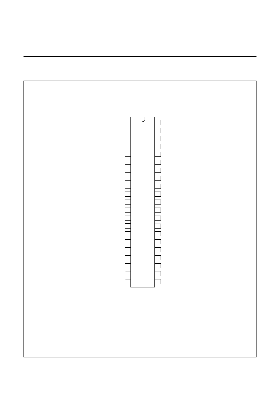
5 PINNING INFORMATION
5.1 Pinning
handbook, halfpage
PWM7/P2.7
PWM6/P2.6
PWM5/P2.5
PWM4/P2.4
PWM3/P2.3
PWM2/P2.2
PWM1/P2.1
PWM0/P2.0
HSYNCin/PROG
HSYNC
CSYNCin/P1.6
VSYNCin/OE
VSYNC
XTAL1
XTAL2
out
out
V
DD
V
SS
/P1.5
/P1.4
P0.7
P0.6
P0.5
P0.4
1
2
3
4
5
6
7
8
9
10
11
12
13
14
15
16
17
18
19
20
P83C880
P83C180
P83C280
P83C380
P87C380
MGG020
42
PWM8/CLAMP/P3.0
41
PWM9/PATOUT/P3.1
40
PWM10/P1.7
39
SCL/P1.0
38
SDA/P1.1
37
SCL1/P1.2
36
SDA1/P1.3
35
INT1/V
PP
34
ADC1/P3.3
33
ADC0/P3.2
V
32
DDA
V
31
SSA
30
DAC3
29
DAC2
28
DAC1
27
DAC0
26
RESET
25
P0.0
24
P0.1
23
P0.2
2221
P0.3
P83Cx80; P87C380
Fig.2 Pinning configuration for SDIP42.
1997 Dec 12 6
Page 7
Philips Semiconductors Product specification
Microcontrollers for monitors with DDC
P83Cx80; P87C380
interface, auto-sync detection and sync proc.
5.2 Pin description
Table 2 Pin description for SDIP42 (SOT270-1)
SYMBOL PIN DESCRIPTION
PWM9/PATOUT/P3.1 41 PWM9 to PWM0: 8-bit Pulse Width Modulation outputs 9 to 0. Pin 41 and 42 can
PWM8/CLAMP/P3.0 42
PWM7/P2.7 1
PWM6/P2.6 2
PWM5/P2.5 3
PWM4/P2.4 4
PWM3/P2.3 5
PWM2/P2.2 6
PWM1/P2.1 7
PWM0/P2.0 8
XTAL1 9 Oscillator input pin for system clock.
XTAL2 10 Oscillator output pin for system clock.
V
DD
V
SS
HSYNC
HSYNC
CSYNC
VSYNC
VSYNC
/PROG 13 Horizontal sync input pin. During OTP programming it is used as the program pulse
in
/P1.5 14 Horizontal sync output pin; alternative function: general I/O port P1.5.
out
/P1.6 15 Composite sync input pin; alternative function: general I/O port P1.6.
in
/OE 16 Vertical sync input pin. During OTP programming it is used as output strobe (OE).
in
/P1.4 17 Vertical sync output pin; alternative function: general I/O port P1.4.
out
P0.7 to P0.0 18 to 25 Port 0: general I/O ports; capability to drive LED.
RESET 26 Reset input; active HIGH initializes the device.
DAC0 to DAC3 27 to 30 8-bit DAC analog voltage output pins; output range: 0 to 5 V.
V
SSA
V
DDA
ADC0/P3.2 33 ADC analog input pins; alternative function: general I/O ports P3.2 and P3.3.
ADC1/P3.3 34
INT1/V
PP
SDA1/P1.3 36 I
SCL1/P1.2 37 I
SDA/P1.1 38 I
SCL/P1.0 39 I
PWM10/P1.7 40 14-bit Pulse Width Modulation output 10; alternative function: general I/O port P1.7.
also be used as the output pin of the test pattern display PATOUT and clamping out
signal CLAMP respectively; PATOUT and CLAMP always have the higher priority.
Alternative function general I/O ports; Port 3: P3.1 to P3.0 and
Port 2: P2.7 to P2.0.
11 Digital power supply (+5 V).
12 Digital ground.
input (PROG).
31 Analog ground for DAC and ADC.
32 Analog power supply (+5 V) for DAC and ADC.
35 External interrupt input pin. During OTP programming it is used as programming
supply voltage pin; VPP= 12.75 V.
2
C-bus serial data I/O port for the DDC2 interface; alternative function: general I/O
port P1.3.
2
C-bus serial clock I/O port for the DDC2 interface; alternative function: general I/O
port P1.2.
2
C-bus serial data I/O port; alternative function: general I/O port P1.1.
2
C-bus serial clock I/O port; alternative function: general I/O port P1.0.
1997 Dec 12 7
Page 8

Philips Semiconductors Product specification
Microcontrollers for monitors with DDC
interface, auto-sync detection and sync proc.
6 FUNCTIONAL DESCRIPTION
This chapter gives a brief overview of the device.
Detailed functional descriptions are given in the following
chapters:
Chapter 7 “Memory organization”
Chapter 8 “Interrupts”
Chapter 9 “Watchdog Timer”
Chapter 10 “Input/Output (I/O)”
Chapter 11 “Reduced power modes”
Chapter 12 “Oscillator”
Chapter 13 “Reset”
Chapter 14 “Analog control (DC)”
Chapter 15 “Analog-to-digital converter (ADC)”
Chapter 16 “Digital-to-analog converter (DAC)”
Chapter 17 “Display Data Channel (DDC) interface”
Chapter 18 “I2C-bus Interface”
Chapter 19 “Hardware mode detection”
Chapter 20 “Power management”
Chapter 21 “Control modes”.
6.1 General
The P83C880, P83C180, P83C280, P83C380 and
P87C380 8-bit microcontrollers are manufactured in an
advanced CMOS process and are derivatives of the
80C51 microcontroller family. They have the same
instruction set as the 80C51.
They contain 512 bytes of data memory (RAM). ROM:
8 kbytes (P83C880); 16 kbytes (P83C180); 24 kbytes
(P83C280); 32 kbytes (P83C380) and 16 kbytes of
EPROM for the P87C180. The microcontrollers are
intended for use in monitors ranging from 14" to 21" that
can be controlled from the outside (e.g. by a PC) via the
external DDC interface.
In addition to the 80C51 standard functions, they provide a
number of dedicated hardware functions for monitor
application. Eight general I/O ports plus 20 functions
combined I/O ports cater for application requirements
adequately.
Ten sets of 8-bit PWM deliver the digital waveform for
analog control purposes. One 14-bit PWM can support
F to V application. The keyboard interface is achieved via
a 4-bit ADC. A Watchdog Timer with a maximum count
period of 5 s prevents the processor running out of control
due to malfunction. Four channels of linear DAC with 8-bit
resolution support more accurate analog controls.
One software I
connection. A DDC interface will cover all DDC protocols,
including DDC1, DDC2B, DDC2AB and DDC2B+.
A hardware mode detector will facilitate mode detection
even in power reduced modes, e.g. Idle mode.
The versatile HSYNC and VSYNC outputs can be
generated to serve the desired application. In the free
running mode, two display patterns can highlight the status
of the monitor. Accordingly, the following items will be
supported by these microcontrollers:
• Mode detection for:
• ACCESS.bus interfacing with external devices, e.g. PCs
• DDC1, DDC2B, DDC2AB and DDC2B+ protocols as
• Device Power Management Signalling (DPMS) as
Figure 1 shows the block diagram functions.
P83Cx80; P87C380
2
C-bus interface is dedicated for the internal
– Horizontal sync (HSYNC) frequencies from below
15 kHz up to 150 kHz
– Vertical sync (VSYNC) frequencies from below 40 Hz
up to 200 Hz
defined in the VESA DDC standard
described in VESA DPMS proposal.
1997 Dec 12 8
Page 9

Philips Semiconductors Product specification
Microcontrollers for monitors with DDC
P83Cx80; P87C380
interface, auto-sync detection and sync proc.
7 MEMORY ORGANIZATION
The Central Processing Unit (CPU) manipulates operands in two memory spaces. There are 512 bytes of internal data
memory, consisting of 256 bytes standard RAM and 256 bytes RAM buffer which is accessible as the Auxiliary RAM
(AUX-RAM) or addressed through DDCADR and RAMBUF. The memory map and address spaces are shown in Fig.3.
INDIRECT
ONLY
INDIRECT
overlapped space
SPECIAL
FUNCTION
REGISTERS
internal data memory area
255
AUX-RAM
BUFFER
INDIRECT
ONLY
0
MGG028
ndbook, full pagewidth
32767
24575
16383
8191
(1) P83C380 and P87C380.
(2) P83C280.
(3) P380C180.
(4) P83C880.
(1)
(2)
(3)
(4)
INTERNAL
0
program memory area
255
127
DIRECT AND
0
Fig.3 Memory map and address spaces.
7.1 Program memory
The program memory consists of ROM: 8 kbytes (P83C880), 16 kbytes (P83C180), 24 kbytes (P83C280) and 32 kbytes
(P83C380). The program memory implemented in the P87C380 is a 16 kbytes EPROM (OTP).
7.2 Internal data memory
The internal data memory is divided into three physically separated parts: 256 bytes of RAM, 256 bytes of AUX-RAM,
and a 128 bytes Special Function Registers (SFRs) area. These can be addressed each in a different way as described
in Sections 7.2.1 to 7.2.3 and Table 3.
Table 3 Internal data memory map
ADDRESS MODE
MEMORY LOCATION
POINTERS
DIRECT INDIRECT
RAM 0 to 127
128 to 255
AUX-RAM 0 to 255 − X
(1)
(2)
X X address pointers are R0 and R1 of the selected register bank
− X
(3)
address pointer DDCADR and RAMBUF
SFRs 128 to 255 X −−
Notes
1. RAM locations 0 to 127 can be addressed directly and indirectly as in the 80C51.
2. RAM locations 128 to 255 can only be addressed indirectly.
1997 Dec 12 9
Page 10

Philips Semiconductors Product specification
Microcontrollers for monitors with DDC
interface, auto-sync detection and sync proc.
3. Indirect-addressable via MOVX-Datapointer or
MOVX-Ri instructions.
7.2.1 RAM
Four register banks, each 8 registers wide, occupy
locations 0 through 31 in the lower RAM area. Only one of
these banks may be enabled at a time. The next 16 bytes,
locations 32 through 47, contain 128 directly addressable
bit locations. The stack can be located anywhere in the
internal 256 bytes RAM. The stack depth is only limited by
the available internal RAM space of 256 bytes (see Fig.4).
7.2.2 S
The SFRs can only be addressed directly in the address
range from 128 to 255 (see Fig.3). Figure 5 gives an
overview of the Special Function Registers space. Sixteen
address in the SFRs space are both byte and
bit-addressable. The bit-addressable SFRs are those
whose address ends in 0H and FH. The bit addresses in
this area are 80H to FFH
7.2.3 AUX-RAM
AUX-RAM buffer 0 to 255 is indirectly addressable as
external data memory locations 0 to 255 via
MOVX-Datapointer instruction or via MOVX-Ri instruction.
Since the external access function is not available, any
access to AUX-RAM 0 to 255 will not affect the ports.
The 256 bytes of AUX-RAM buffer used to support DDC
interface is also available for system usage by indirect
addressing through the address pointer DDCADR and
data I/O buffer RAMBUF. The address pointer (DDCADR)
is equipped with the post increment capability to facilitate
the transfer of data in bulk (for details refer to Chapter 17).
However, it is also possible to address the AUX-RAM
buffer through MOVX command as usually used in the
internal RAM extension of 80C51 derivatives.
PECIAL FUNCTION REGISTERS (SFRS)
BYTE
ADDRESS
(HEX)
FFH
2FH
2EH
2DH
2CH
2BH
2AH
29H
28H
27H
26H
25H
24H
23H
22H
21H
20H
1FH
18H
17H
10H
0FH
08H
07H
00H
P83Cx80; P87C380
BIT ADDRESS
(HEX)
(MSB) (LSB)
7F 7E 7D 7C 7B 7A 79 78
77 76 75 74 73 72 71 70
6F 6E 6D 6C 6B 6A 69 68
67 66 65 64 63 62 61 60
5F 5E 5D 5C 5B 5A 59 58
57 56 55 54 53 52 51 50
4F 4E 4D 4C 4B 4A 49 48
47 46 45 44 43 42 41 40
3F 3E 3D 3C 3B 3A 39 38
37 36 35 34 33 32 31 30
2F 2E 2D 2C 2B 2A 29 28
27 26 25 24 23 22 21 20
1F 1E 1D 1C 1B 1A 19 18
17 16 15 14 13 12 11 10
0F 0E 0D 0C 0B 0A 09 08
07 06 05 04 03 02 01 00
BANK 3
BANK 2
BANK 1
BANK 0
MBH079
BYTE
ADDRESS
(DECIMAL)
255
47
46
45
44
43
42
41
40
39
38
37
36
35
34
33
32
31
24
23
16
15
8
7
0
1997 Dec 12 10
Fig.4 RAM bit addresses.
Page 11

Philips Semiconductors Product specification
Microcontrollers for monitors with DDC
interface, auto-sync detection and sync proc.
handbook, full pagewidth
BYTE ADDRESS
(HEX)
FFH
F8H
F0H F6 F5 F4 F3 F2 F1 F0
E8H EE ED EC EB EA E9 E8
E0H E6 E5 E4 E3 E2 E1 E0
D8H
(MSB) (LSB)
FF
FE FD FC FB FA F9 F8
F7
EF
E7
DF
DE DD DC DB DA D9 D8
BIT ADDRESS
(HEX)
P83Cx80; P87C380
BYTE ADDRESS
(DECIMAL)
255
MDCST
B
PWME2
ACC
S1CON
D0H
C8H
C0H C6 C5 C4 C3 C2 C1 C0
B8H BE BD BC BB BA B9 B8
B0H B6 B5 B4 B3 B2 B1 B0
A8H AE AD AC AB AA A9 A8
A0H A6 A5 A4 A3 A2 A1 A0
98H 9E 9D 9C 9B 9A 99 98
90H 96 95 94 93 92 91 90
88H 8E 8D 8C 8B 8A 89 88
80H 86 85 84 83 82 81 80
D7 D6 D5 D4 D3 D2 D1 D0
CF CE CD CC CB CA C9 C8
C7
BF
B7
AF
A7
9F
97
8F
87
MGG029
PSW
PWME1
DFCON
IP0
P3
IEN0
P2
not used
P1
TCON
P0
Fig.5 Special Function Registers bit addresses.
1997 Dec 12 11
Page 12

Philips Semiconductors Product specification
Microcontrollers for monitors with DDC
P83Cx80; P87C380
interface, auto-sync detection and sync proc.
7.3 Additional Special Function Registers
The standard SFRs as used in 80C51 and the SFRs for some typical derivative functions like I2C-bus interface, Timer,
etc. are described in the
chapters. Some SFRs which are not mentioned or not dedicated to a certain function will be described in the following
sections.
All new additional SFRs used in the P83C880 are listed in Table 4. However, only some of them will be explained in detail
in Sections 7.3.1 to 7.3.7.
Table 4 Overview of additional SFRs
REGISTER DESCRIPTION ADDRESS RESET VALUE
RAMBUF RAM Buffer I/O Interface Register 9CH XXXXXXXX B
DDCCON DDC Control Register 9DH X00X0000 UBBUBBBB
DDCADR DDC Address Pointer 9EH 00000000 B
DDCDAT Data Shift Register for DDC1 9FH 00000000 B
DFCON Miscellaneous Control Register C0H 10000000 B
ADCDAT ADC Control Register C1H XX000000 UUBBBBBR
PWM10H PWM High-byte Data Latch C6H 00000000 B
PWM10L PWM Low-byte Data Latch C7H 10000000 B
S1CON Control Register for DDC2 D8H 00000000 B
S1STA Status Register for DDC2 D9H 11111000 R
S1DAT Data Shift Register for DDC2 DAH 00000000 B
S1ADR Address Register for DDC2 DBH 00000000 B
PWME1 PWM Output Control Register 1 C8H 00000000 B
PWME2 PWM Output Control Register 2 E8H 00000000 B
PWM0 to PWM9 Data Latches for 8-bit PWMs C9H to CFH,
DAC0 to DAC3 8-bit Data Latches for 8-bit DACs E9H to ECH 00000000 B
HFP Free run Control Register for HSYNC
HFPOPW Free run and Pulse width for HSYNC
MDCST Mode Detect Control and Status Register F8H 1X000000 BUBBRRRR
VFP Free run Control Register for VSYNC
VFPOPW Free run and Pulse width for VSYNC
PULCNT Pulse Generation Control Register FBH 00000000 B
HFHIGH Horizontal Period Counting High-byte
VFHIGH Vertical Period Counting High-byte Register FDH 00000000 R
VFLHFL Vertical and Horizontal Period Counting
T2 Watchdog Timer Data Register FFH 00000000 B
“Data Handbook IC20”
Register
Low-nibbles Register
. The specific SFRs for the P83C880 are introduced in the relevant
(1)
READ/WRITE
o
00000000 B
EDH to EFH
out
out
out
out
F6H 01100000 B
F7H 00011111 B
F9H 01000000 B
FAH XX000101 B
FCH 00000000 R
FEH 00000000 R
o
o
o
(2)
O
Notes
1. X = don’t care; even if it’s implemented.
2. B = both read/write and R
= read only; accessible for the entire byte or an individual bit. U = not implemented.
o
1997 Dec 12 12
Page 13
Philips Semiconductors Product specification
Microcontrollers for monitors with DDC
P83Cx80; P87C380
interface, auto-sync detection and sync proc.
7.3.1 RAM BUFFER I/O INTERFACE REGISTER (RAMBUF)
RAMBUF is used as an I/O interface to the RAM buffer. If it is associated with the address pointer DDCADR which is
equipped with the capability of post increment, then it will be convenient to transfer the consecutive data stream. This
feature is useful to support the DDC/EDID data transfer.
Table 5 RAM Buffer I/O Interface Register (SFR address 9CH)
76543210
RAMBUF.7 RAMBUF.6 RAMBUF.5 RAMBUF.4 RAMBUF.3 RAMBUF.2 RAMBUF.1 RAMBUF.0
Table 6 Description of RAMBUF bits
BIT SYMBOL DESCRIPTION
7 to 0 RAMBUF.7 to RAMBUF.0 8-bit data which is read from or to be written into RAM buffer
7.3.2 M
This register is bit-addressable.
Table 7 Miscellaneous Control Register (SFR address C0H)
ISCELLANEOUS CONTROL REGISTER (DFCON)
76543210
EW2 SOGE SYNCE DDCE S1E ADCE P14LVL P8LVL
Table 8 Description of DFCON bits
BIT SYMBOL DESCRIPTION
7 EW2 Watchdog Timer enable flag. This flag is associated with the flags, EW1 (SFR
PWM10H) and EW0 in (SFR PWM10L) to form the enable/disable control key for the
Watchdog Timer (see Chapter 9). The Watchdog Timer is only disabled by
EW2 to EW0 = 101, else it is kept enabled for the rest of the combinations.
6 SOGE CSYNC
enable for pin CSYNCin/P1.6. If SOGE = 1, the pin function is CSYNCin. If
in
SOGE = 0, the pin function is I/O port P1.6.
5 SYNCE Sync separated signals output enable for pins VSYNC
If SYNCE = 1, the pins function as VSYNC
and HSYNC
out
/P1.4 and HSYNC
out
respectively.
out
out
If SYNCE = 0, the pins function as I/O ports P1.4 and P1.5 respectively.
4 DDCE Enable for DDC interface pins SCL1/P1.2 and SDA1/P1.3. If DDCE = 1, the pins
function as SCL1 and SDA1 respectively for the DDC interface. If DDCE = 0, the pins
function as I/O ports P1.2 and P1.3 respectively.
3 S1E Enable for I
2
C-bus interface pins SCL/P1.0 and SDA/P1.1. If S1E = 1, the pins
function as SCL and SDA respectively for the I2C-bus interface. If S1E = 0, the pins
function as I/O ports P1.0 and P1.1 respectively.
/P1.5.
1997 Dec 12 13
Page 14
Philips Semiconductors Product specification
Microcontrollers for monitors with DDC
P83Cx80; P87C380
interface, auto-sync detection and sync proc.
BIT SYMBOL DESCRIPTION
2 ADCE ADC channel enable. This flag enables the ADC function and also switches the pins
ADC0/P3.2 and ADC1/P3.3 to the ADC inputs function. If ADCE = 1, the ADC function
is enabled and the pin functions are ADC0 and ADC1 respectively. If ADCE = 0, the
ADC function is disabled and the pin functions are I/O ports P3.2 and P3.3 respectively.
1 P14LVL Polarity selection bit for the PWM10 output (14-bit PWM). If P14LVL = 1, PWM10
output is inverted. If P14LVL = 0, PWM10 output is not inverted.
0 P8LVL Polarity selection bit for the PWM0 to PMM9 outputs (8-bit PWM). If P8LVL = 1,
PWM0 to PWM9 outputs are inverted. If P8LVL= 0, PWM0 to PWM9 outputs are not
inverted.
7.3.3 ADC CONTROL REGISTER (ADCDAT)
Table 9 ADC Control Register (SFR address C1H)
76543210
−−DACHL DAC3 DAC2 DAC1 DAC0 COMP
Table 10 Description of ADCDAT bits
BIT SYMBOL DESCRIPTION
7 to 6 − Reserved.
5 DACHL ADC input channels selection. If DACHL = 1, then input channel
ADC1 is selected. If DACHL = 0, then input channel ADC0 is selected.
4 to 1 DAC3 to DAC0 Reference voltage level selection. The 4 bits select the analog output
voltage (V
0 COMP Comparison result; read only. If COMP = 1, then the ADC input
voltage is higher than the reference voltage. If COMP = 0, then the ADC
input voltage is lower than the reference voltage.
7.3.4 14-
Table 11 PWM High-byte Data Latch (PWM10H; SFR address C6H)
EW1 PWM10H.6 PWM10H.5 PWM10H.4 PWM10H.3 PWM10H.2 PWM10H.1 PWM10H.0
Table 12 Description of PWM10H bits
6 to 0 PWM10H.6 to PWM10H.0 7 upper data bits for the 14-bit PWM.
BIT PWM DATA LATCHES (PWM10H AND PWM10L)
76543210
BIT SYMBOL DESCRIPTION
7 EW1 Watchdog Timer enable flag. This flag is associated with the flag EW2
(SFR DFCON) and EW0 (SFR PWM10L) to form the enable/disable
control key for the Watchdog Timer; see Tables 8 and 14.
) of the 8-bit DAC. For V
ref
values see Table 31.
ref
1997 Dec 12 14
Page 15

Philips Semiconductors Product specification
Microcontrollers for monitors with DDC
P83Cx80; P87C380
interface, auto-sync detection and sync proc.
Table 13 PWM Low-byte Data Latch (PWM10L; SFR address C7H)
76543210
EW0 PWM10L.6 PWM10L.5 PWM10L.4 PWM10L.3 PWM10L.2 PWM10L.1 PWM10L.0
Table 14 Description of PWM10L bits
BIT SYMBOL DESCRIPTION
7 EW0 Watchdog Timer enable flag. This flag is associated with the flag EW2
(SFR DFCON) and EW1 (SFR PWM10H) to form the enable/disable
control key for the Watchdog Timer; see Table 8 and 12.
6 to 0 PWM10L.6to PWM10L.0 7 lower data bits for the 14-bit PWM.
7.3.5 PWM O
Table 15 PWM Output Control Register 1 (SFR address C8H)
76543210
PWME1.7 PWME1.6 PWME1.5 PWME1.4 PWME1.3 PWME1.2 PWME1.1 PWME1.0
Table 16 Description of PWME1 bits
UTPUT CONTROL REGISTER 1 (PWME1)
BIT SYMBOL DESCRIPTION
7 to 0 PWME1.7
to
PWME1.0
PWM outputs enable; n=7to0. If PWME1.n = 1, the corresponding PWM is enabled
and pins PWMn/P2.n are switched to PWMn outputs. If PWME1.n = 0, the
corresponding PWM is disabled and pins PWMn/P2.n are switched to I/O ports P2.n
function.
1997 Dec 12 15
Page 16

Philips Semiconductors Product specification
Microcontrollers for monitors with DDC
P83Cx80; P87C380
interface, auto-sync detection and sync proc.
7.3.6 PWM OUTPUT CONTROL REGISTER 2 (PWME2)
Table 17 PWM Output Control Register 2 (SFR address E8H)
76543210
PATENA DACE3 DACE2 DACE1 DACE0 PWME2.2 PWME2.1 PWME2.0
Table 18 Description of PWME2 bits
BIT SYMBOL DESCRIPTION
7 PATENA PATOUT (pattern output) enable. If PATENA = 1, the pin
PWM9/PATOUT/P3.1 is switched to the PATOUT (display test pattern)
output. If PATENA = 0, the PATOUT function is disabled. The PATOUT
function always overrides other alternative functions such as PWM9 and
P3.1.
6 to 3 DACE3 to DACE0 DAC outputs enable (n=3to0). If DACEn = 1, the corresponding
DACs: DAC3 to DAC0 are enabled. If DACEn = 0, the corresponding
DACs: DAC3 to DAC0 are disabled.
2 to 0 PWME2.2 to PWME2.0 PWM outputs enable; n = 2 to 0. If PWME2.n = 1, the corresponding
PWMs: PWM8, PWM9 and PWM10, are enabled by PWME2.2,
PWME2.1 and PWME2.0 respectively and pins PWM8/CLAMP/P3.0,
PWM9/PATOUT/P3.1 and PWM10/P1.7 are switched to PWM output. If
PWME2.n = 0, the corresponding PWM is disabled. Pins
PWM8/CLAMP/P3.0, PWM9/PATOUT/P3.1 and PWM10/P1.7 are
switched to I/O port functions P3.0, P3.1 and P1.7 respectively.
7.3.7 D
Table 19 Data Latches for 8-bit PWMs (n = 0 to 9; SFR address C9H to CFH and EDH to EFH)
PWMn.7 PWMn.6 PWMn.5 PWMn.4 PWMn.3 PWMn.2 PWMn.1 PWMn.0
Table 20 Description of PWM0 to PWM9 bits
ATA LATCHES FOR 8-BIT PWMS (PWM0 TO PWM9)
76543210
BIT SYMBOL DESCRIPTION
7 to 0 PWMn.7 to PWMn.0 8-bit data for PWM channel n (n = 0 to 9)
1997 Dec 12 16
Page 17

Philips Semiconductors Product specification
Microcontrollers for monitors with DDC
interface, auto-sync detection and sync proc.
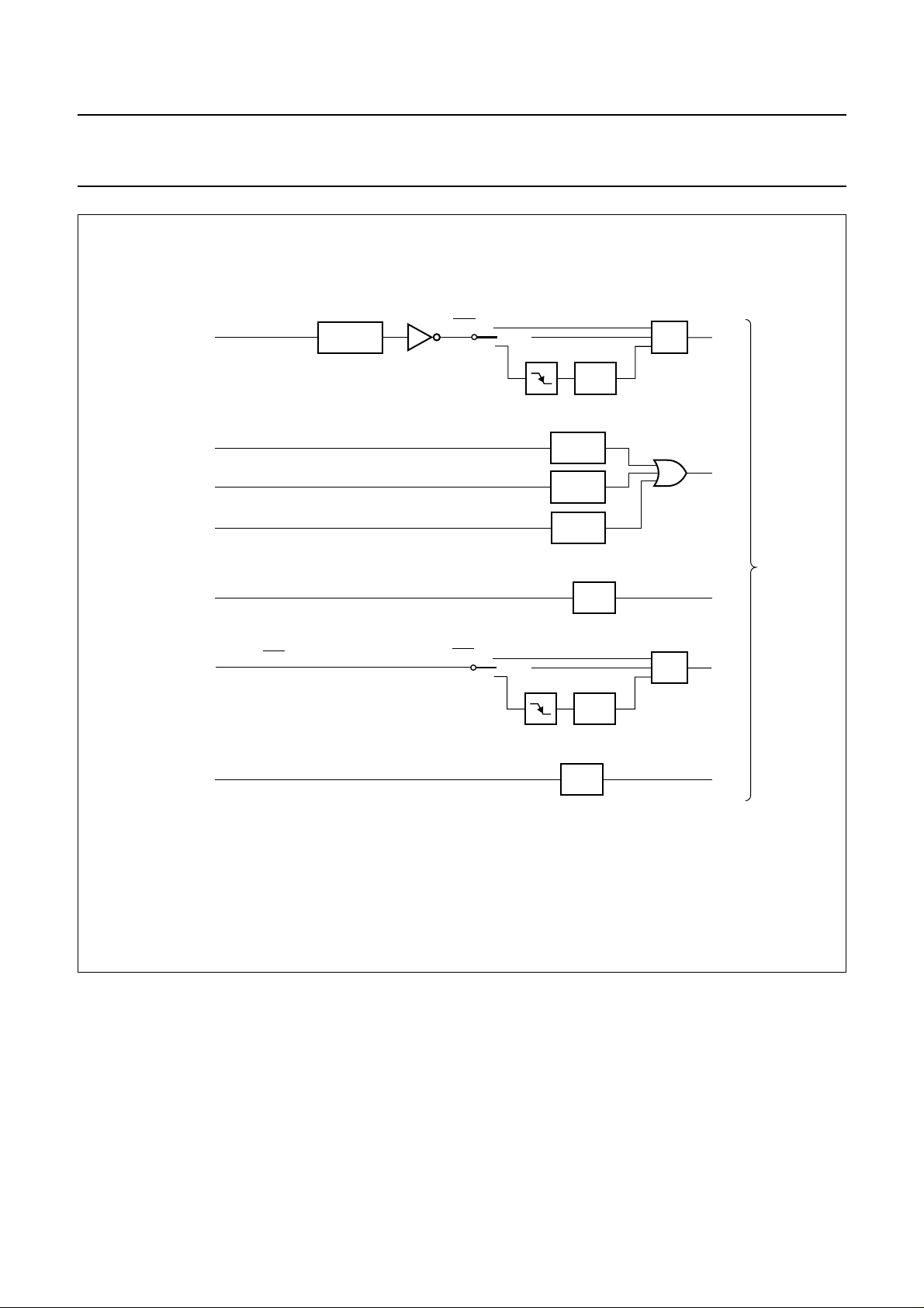
8 INTERRUPTS
The P83C880 has 5 interrupt sources; these are shown in
Fig.6.
Interrupt INT1 is generated as in a normal 80C51 device.
By means of IT1 in SFR TCON this interrupt can be
selected to be:
• Level sensitive, when IT1 = LOW; INT1 must be inactive
before a return from interrupt instruction (RETI) is given,
otherwise the same interrupt will occur again.
• Edge sensitive, when IT1 = HIGH; the internal hardware
will reset the latch when the LCALL instruction is
executed for the vector address (see Table 21).
Interrupt
detector. Interrupt INT0 is selected as edge or level
sensitive by the state of the IT0 bit in the SFR TCON.
However, it is recommended to always set IT0 to HIGH
(edge sensitive) so that IE0 will be reset by the internal
hardware when the LCALL instruction is executed for the
vector address.
Timer 0 and Timer 1 interrupts are generated by TF0 and
TF1 which are set by an overflow of their respective
Timer/Counter registers (except for Timer 0 in Mode 3;
see
Timer/Counters”
interrupt flag is cleared by the internal hardware when the
LCALL instruction is executed for the vector address.
The DDC interrupt is generated either by bit SI (SFR
S1CON) for DDC2B/DDC2AB/DDC2B+ protocols or by bit
DDC_int (SFR DDCCON) or by bit SWHINT (SFR
DDCCON). These flags must be cleared by software.
All bits that generate interrupts can be set or cleared by
software, with the same result as though it had been set or
cleared by hardware. That is, interrupts can be generated
or pending interrupts can be cancelled in software.
INT0 is generated by the mode change of mode
“Data Handbook IC20; 80C51 Family; Chapter
). When a timer interrupt is generated, the
Each of these interrupts sources can be individually
enabled or disabled by setting or clearing the bit in Special
Function Register IE (see Table 23). IE also contains a
global disable bit EA, which disables all interrupts at once.
8.1 Priority level structure
The priority level of each interrupt source can be
individually programmed by setting or clearing a bit in
Special Function Register IP (see Table 25). A low priority
interrupt can itself be interrupted by a high priority
interrupt, but not by another low priority interrupt. A high
priority interrupt can not be interrupted by another interrupt
source.
If two requests of different priority levels are received
simultaneously, the request of higher priority level is
serviced. If request of the same priority level is received
simultaneously, an internal polling sequence determines
which request is serviced. Thus within each priority level
there is a second priority structure determined as shown in
Table 21. The IP register contains a number of reserved
(in 80C51) bits: IP.7, IP.6 and IP.4. User software should
not write logic 1s to these positions, since they may be
used in other 80C51 family products.
Table 21 Priority within levels
Note
1. The ‘Priority within level’ structure is only used to
P83Cx80; P87C380
SOURCE PRIORITY WITHIN LEVEL
IE0′ 1 (highest)
SI 2
TF0 3
IE1′ 4
TF1 5 (lowest)
resolve simultaneous requests of the same priority
level.
(1)
1997 Dec 12 17
Page 18
Philips Semiconductors Product specification
Microcontrollers for monitors with DDC
interface, auto-sync detection and sync proc.
handbook, full pagewidth
mode change interrupt
SWITCH interrupt
DDC1 interrupt
DDC2 (DDC2B/DDC2AB/DDC2B+) interrupt
Timer 0 overflow
CHREQ
INT0
'0'
IT0
'1'
IE0
SWH INT
DDC INT
S12
TF0
P83Cx80; P87C380
MUX
IE0´
SI
interrupt
sources
TF0
external interrupt INT1
Timer 1 overflow
'0'
INT1
IT1
'1'
Fig.6 Interrupt sources.
TF1
IE1
MUX
IE1´
TF1
MGG024
1997 Dec 12 18
Page 19

Philips Semiconductors Product specification
Microcontrollers for monitors with DDC
interface, auto-sync detection and sync proc.
8.2 How interrupts are handled
The interrupt flags are sampled at the S5P2 state of every
machine cycle. The samples are polled during the
following machine cycle. If one of the flags was in a set
condition at S5P2 of the preceding cycle, the polling cycle
will find it and the interrupt system will generate an LCALL
to the appropriate service routine, provided this hardware
generated LCALL is not blocked by any of the following
conditions:
1. An interrupt of equal priority or higher priority level is
already in progress.
2. The current (polling) cycle is not the final cycle in the
execution of the instruction in progress.
3. The instruction in progress is RETI or any write to the
IE or IP registers.
Any of these conditions will block the generation of the
LCALL to the interrupt service routine. Condition 2
ensures that the instruction in progress will be completed
before vectoring to any service routine.
Condition 3 ensures that if the instruction in progress is
RETI or any access to IE or IP, then at least one more
instruction will be executed before the interrupt is vectored
to.The polling cycle is repeated with each machine cycle,
and the values polled are the values that were present at
S5P2 of the previous machine cycle. Note that if an
interrupt flag is active but not being responded to for one
of the above mentioned conditions, and if the flag is still
inactive when the blocking condition is removed, then the
denied interrupt will not be serviced. In other words, the
fact that the interrupt flag was once active but not serviced
is not remembered. Every polling cycle is new.
The polling cycle/LCALL sequence is illustrated in
“Data
Handbook IC20; 80C51 family hardware description;
Figure: Interrupt Response Timing Diagram”
.
Note that if an interrupt of higher priority level becomes
active prior to S5P2 of the machine cycle labelled C3 (see
“Data Handbook IC20; 80C51 family hardware description;
Figure: Interrupt Response Timing Diagram”
accordance with the above rules it will be vectored to
during C5 and C6, without any instruction of the lower
priority routine having been executed. Thus the processor
acknowledges an interrupt request by executing a
hardware generated LCALL to the appropriate servicing
routine. The hardware generated LCALL pushes the
contents of the Program Counter on to the stack (but it
does not save the PSW) and reloads the PC with an
address that depends on the source of the interrupt being
vectored to as shown in Table 22.
Execution proceeds from that location until the RETI
instruction is encountered. The RETI instruction informs
the processor that the interrupt routine is no longer in
progress, then pops the top two bytes from the stack and
reloads the Program Counter. Execution of the interrupted
program continues from where it left off.
Note that a simple RET instruction would also return
execution to the interrupted program, but it would have left
the interrupt control system thinking an interrupt was still in
progress, making future interrupts impossible.
Table 22 Vector addresses
P83Cx80; P87C380
), then in
SOURCE VECTOR ADDRESS
IE0′ 0003H
SI 002BH
TF0 000BH
IE1′ 0013H
TF1 001BH
1997 Dec 12 19
Page 20
Philips Semiconductors Product specification
Microcontrollers for monitors with DDC
P83Cx80; P87C380
interface, auto-sync detection and sync proc.
8.3 Interrupt Enable Register (IE)
Table 23 Interrupt Enable Register (SFR address A8H)
76543210
EA − ES1 − ET1 EX1 ET0 EX0
Table 24 Description of IE bits
BIT SYMBOL FUNCTION
7EADisable all interrupts. If EA = 0, then no interrupt will be acknowledged. If EA = 1, then
each interrupt source is individually enabled or disabled by setting or clearing its enable
bit.
6 − Reserved.
5 ES1 Enable DDC interface interrupt. If ES1 = 1, then DDC interface interrupt is enabled.
If ES1 = 0, then DDC interface interrupt is disabled.
4 − Reserved.
3 ET1 Enable Timer 1 overflow interrupt. If ET1 = 1, then the Timer 1 interrupt is enabled.
If ET1 = 0, then the Timer 1 interrupt is disabled.
2 EX1 Enable external interrupt 1. If EX1 = 1 then the External 1 interrupt is enabled.
If EX1 = 0 then the External 1 interrupt is disabled.
1 ET0 Enable Timer 0 overflow interrupt. If ET0 = 1 then the Timer 0 interrupt is enabled.
If ET0 = 0 then the Timer 0 interrupt is disabled.
0 EX0 Enable mode change. If EX0 = 1 then the mode change interrupt is enabled.
If EX0 = 0 then the mode change interrupt is disabled.
8.4 Interrupt Priority Register (IP)
Table 25 Interrupt Priority Register (address B8H)
76543210
−−PS1 − PT1 PX1 PT0 PX0
Table 26 Description of IP bits
BIT SYMBOL DESCRIPTION
7to6 − Reserved.
5 PS1 DDC interface Interrupt priority level. When PS1 = 1, DDC interface Interrupt is
assigned a high priority level.
4 − Reserved.
3 PT1 Timer 1 overflow interrupt priority level. When PT1 = 1, Timer 1 Overflow Interrupt is
assigned a high priority level.
2 PX1 External interrupt 1 priority level. When PX1 = 1, External Interrupt 1 priority is
assigned a high priority level.
1 PT0 Timer 0 overflow interrupt priority level. When PT0 = 1, Timer 0 Overflow Interrupt is
assigned a high priority level.
0 PX0 Mode change interrupt priority level. When PX0 = 1, Mode change Interrupt is
assigned a high priority level.
1997 Dec 12 20
Page 21

Philips Semiconductors Product specification
Microcontrollers for monitors with DDC
interface, auto-sync detection and sync proc.
9 WATCHDOG TIMER
In addition to the standard timers, a Watchdog Timer
consisting of an 10-bit prescaler and an 8-bit timer is also
incorporated. The timer is increased every 19.5 ms for an
oscillator frequency of 16 MHz; this is derived from the
oscillator frequency (f
f
f
timer
=
clk
----------------------------304 1024×
) by the formula:
clk
When a timer overflow occurs, the microcontroller is reset.
To prevent a system reset, the timer must be reloaded
before an overflows occurs, by the application software.
If the processor suffers a hardware/software malfunction,
the software will fail to reload the timer. This failure will
produce a reset upon overflow thus preventing the
processor running out of control.
The Watchdog Timer can only be reloaded if the condition
flag WLE (PCON.4) has been previously set by software.
At the moment the counter is loaded the condition flag is
automatically cleared.
In the Idle mode the Watchdog Timer and reset circuitry
remain active.
The time interval between timer reloading and the
occurrence of a reset, depends on the reloaded value.
The Watchdog Timer’s time interval is:
tt
Where T2 = decimal value of the T2 register contents and
t
1
and t1=19µs (f
For example, this may range from 19.5 ms to 5.0 s when
using an oscillator frequency of 16 MHz.
Table 27 lists the resolution and the maximum time interval
of the Watchdog Timer using different system clocks.
The Watchdog Timer is controlled by the Watchdog control
bits:
• EW2; DFCON.7 (SFR address C0H)
• EW1; PWM10H.7 (SFR address C6H)
• EW0; PWM10L.7 (SFR address C6H).
Only when EW2 to EW0 = 101 the Watchdog Timer is
disabled and allows the Power-down mode to be enabled.
The rest of pattern combinations will keep the Watchdog
Timer enabled and disable the Power-down mode.
This security key with multiple flags split in two SFRs will
prevent the Watchdog Timer from being terminated
abnormally when the function of the Watchdog Timer is
needed.
1024
×=
-----------------------------
1
256 T2–()
= 15.2 µs (f
P83Cx80; P87C380
= 10 MHz); t1= 12.7 µs (f
clk
= 16 MHz).
clk
= 12 MHz)
clk
Table 27 Resolution and the maximum time interval of the WDT
f
clk
(MHz)
PRESCALER FACTOR
RESOLUTION
10 152 15.56 4.0
12 12.97 3.3
16 304 19.46 5.0
(ms)
MAXIMUM TIME INTERVAL
(s)
1997 Dec 12 21
Page 22

Philips Semiconductors Product specification
Microcontrollers for monitors with DDC
interface, auto-sync detection and sync proc.
10 INPUT/OUTPUT (I/O)
The P83C880 has three 8-bit ports. Ports 0 to 2 are the
same as in the 80C51, with the exception of the additional
functions of Port 1 and Port 2. Port 3 only contains 4 bits.
Port 3 also has alternative functions.
All ports are bidirectional. Pins of which the alternative
function is not used may be used as normal bidirectional
I/Os.
The use of Port 1, Port 2 and Port 3 pins as an alternative
function is carried out automatically by the P83C880
provided the associated Special Function Register bit is
set HIGH.
The quasi-bidirectional type of port is applied for Port 1,
Port 2 and Port 3. Port 0 is an open-drain I/O port with the
capability to drive LED. However, for any port with an
alternative function, while the alternative function is
performed, the port type will be switched to the appropriate
type against a specific function. The port types:
quasi-bidirectional, pull-up and open-drain are shown in
Figs 7, 8 and 9 respectively.
10.1 The alternative functions for Port 0, Port 1,
Port 2 and Port 3
Port 0 Provides the low-order address in
programming/verify mode for the P87C380.
Port 1 Used for a number of special functions:
• 2 I/O pins for I
2
C-bus interface: SCL/P1.0 and
SDA/P1.1. The port type in this situation is set as
open-drain.
• 2 I/O pins for DDC interface: SCL1/P1.2 and
SDA1/P1.3. The port type in this situation is set
as open-drain.
• 2 I/O pins for the outputs of sync separation:
VSYNC
/P1.4 and HSYNC
out
/P1.5. The port
out
type in this situation is set as push-pull.
• One pin for the composite sync input of sync on
green mode: CSYNCin/P1.6. There is no pull-up
protection diode for this input pin.
• One pin for the 14-bit PWM output:
PWM10/P1.7. As PWM function, the port type is
open-drain.
Port 2 Two alternative functions are provided:
Port 3 Two alternative functions are provided:
10.2 EMI (Electromagnetic Interference) reduction
In order to reduce EMI (Electromagnetic Interference) the
following design measures have been taken:
• Slope control is implemented on all the I/O lines with
• Placing the VDD and VSS pins next to each other
• Double bonding of the VDD and VSS pins,
• Limiting the drive capability of clock drivers and
• Applying slew rate controlled output drivers
• Internal decoupling of the supply of the CPU core.
P83Cx80; P87C380
• High-order address in Programming/Verify mode
for P87C380.
• 8 channels of PWM outputs:
PWM0/P2.0 to P2.7/PWM7. The port type in this
situation is set as open-drain.
• Two channels of PWM output:
PWM8/CLAMP/P3.0 and PWM9/PATOUT/P3.1.
The port type in this situation is set as
open-drain. PATOUT and CLAMP functions
always override PWM or port function even if
they are enabled. For the PATOUT (pattern
output) and CLAMP (clamping output)
application, the port type is defined as push-pull.
• Two pins for the software ADC input: ADC0/P3.2
and ADC1/P3.3. They are analog inputs.
alternative functions of the PWM, I2C-bus and DDC
interface. For port pins P1.4 and P1.5, since the
alternative functions VSYNC
incorporated, the driving capability is made as small as
possible to reduce radiation and the slope control
function is disabled to have a sharp output. Rise and fall
time (10% to 90%) for slope control are:
t
< rise/fall time < t
rf(min)
rf(max)
Refer to Chapter 27 for the detailed figures.
i.e. 2 bondpads for each pin
prechargers
and HSYNC
out
.
out
are
1997 Dec 12 22
Page 23
Philips Semiconductors Product specification
Microcontrollers for monitors with DDC
interface, auto-sync detection and sync proc.
handbook, full pagewidth
from port latch
read port pin
handbook, full pagewidth
input data
2 oscillator
periods
Q
Fig.7 Standard output with quasi-bidirectional port.
2 oscillator
'1'
periods
strong pull-up
INPUT
BUFFER
strong pull-up
p1
n
p1
P83Cx80; P87C380
V
DD
p2
p3
I/O PIN
I1
MGG025
V
DD
p2
p3
from port latch
read port pin
handbook, full pagewidth
from port latch
read port pin
input data
input data
I/O PIN
Q
INPUT
BUFFER
n
I1
MGG026
Fig.8 Standard output with the pull-up current source.
strong pull-up
2 oscillator
'0'
Q
periods
INPUT
BUFFER
p1
n
p2
I1
V
DD
I/O PIN
MGG027
Fig.9 Standard output with the open-drain port.
1997 Dec 12 23
Page 24

Philips Semiconductors Product specification
Microcontrollers for monitors with DDC
interface, auto-sync detection and sync proc.
11 REDUCED POWER MODES
Two software selectable modes of reduced power
consumption are implemented. These are the Idle mode
and the Power-down mode.
11.1 Power Control Register (PCON)
The Idle mode and Power-down mode are activated by
software via the Power Control Register (SFR PCON).
Its hardware address is 87H. PCON is not bit addressable.
The reset value of PCON is 00H.
11.2 Idle mode
Idle mode operation permits the interrupts, I
interface, DDC interface, mode detection and timer blocks
T0, T1 and T2 (Watchdog Timer) to function while the CPU
is halted. The following functions are switched off when the
microcontroller enters the Idle mode:
• CPU (halted)
• PWM0 to PWM10 (reset, output = HIGH)
• 4-bit ADC (aborted if conversion is in progress)
• DAC0 to DAC3 (output = indeterminate or frozen at the
final value prior to the Idle instruction; decided by
software).
The following functions remain active during Idle mode;
these functions may generate an interrupt or reset and
thus terminate the Idle mode:
• Timer 0, Timer 1 and Timer 2 (Watchdog Timer)
• The DDC interface
• External interrupt
• Mode detection.
The instruction that sets PCON.0 is the last instruction
executed in the normal operating mode before Idle mode
is activated. Once in the Idle mode, the CPU status is
preserved in its entirety: the Stack Pointer, Program
Counter, Program Status Word, Accumulator, RAM and all
other registers maintain their data during Idle mode.
The status of external pins during Idle mode is shown in
Table 28.
There are three ways to terminate the Idle mode:
• Activation of any enabled interrupt X0, T0, X1, T1 or S1
will cause PCON.0 to be cleared by hardware
terminating Idle mode. The interrupt is serviced, and
following return from interrupt instruction RETI, the next
instruction to be executed will be the one which follows
the instruction that wrote a logic 1 to PCON.0.
2
C-bus
• The second way of terminating the idle mode is with an
• The third way of terminating the Idle mode is by an
In all cases the microcontroller restarts after 3 machine
cycles.
11.3 Power-down mode
In Power-down mode the system clock is halted. The
oscillator is frozen after setting the bit PD in the PCON
register.
The instruction that sets PCON.1 is the last executed prior
to going into the Power-down mode. Once in Power-down
mode, the oscillator is stopped.The content of the on-chip
RAM and the Special Function Registers are preserved.
Note that Power-down mode can not be entered when the
Watchdog Timer has been enabled.
The Power-down mode can be terminated by an external
reset in the same way as in the 80C51 (but the SFRs are
cleared due to RESET) or in addition by the external
interrupt, INT1.
A termination with INT1 does not affect the internal data
memory and the Special Function Registers. This gives
the possibility to exit from Power-down without changing
the port output levels. To terminate the Power-down mode
with an external interrupt, INT1 must be switched to be
level-sensitive and must be enabled. The external interrupt
input signal INT1 must be kept LOW till the oscillator has
restarted and stabilized. The instruction following the one
that put the device into the Power-down mode will be the
first one which will be executed after the wake-up.
P83Cx80; P87C380
The flag bits GF0 and GF1 may be used to determine
whether the interrupt was received during normal
execution or during Idle mode. For example, the
instruction that writes to PCON.0 can also set or clear
both flag bits. When Idle mode is terminated by an
interrupt, the service routine can examine the status of
the flag bits.
external hardware reset. Since the oscillator is still
running, the hardware reset is required to be active for
two machine cycles (24 oscillator periods) to complete
the reset operation.
internal watchdog reset.
1997 Dec 12 24
Page 25

Philips Semiconductors Product specification
Microcontrollers for monitors with DDC
P83Cx80; P87C380
interface, auto-sync detection and sync proc.
11.4 Status of external pins
• If the HSYNC
, VSYNC
out
, PATOUT or CLAMP output
out
is selected (for selection see description in Tables 8
and 18) in Idle or Power-down mode, since sync
separation is still alive in Idle mode, HSYNC
VSYNC
, PATOUT or CLAMP output will be operating
out
as normal. In Power-down mode: HSYNC
out
, VSYNC
out
,
out
PATOUT or CLAMP output are pulled HIGH.
• In Idle or Power-down mode, if bit DDCE (SFR DFCON)
is set, the function of P1.2 and P1.3 will be switched to
Table 28 Status of external pins during Idle and Power-down modes
HSYNC;
VSYNC;
CLAMP;
PATOUT
MODE MEMORY
PORT0
TO
PORT 3
Idle internal data operative High-Z operative HIGH unknown
Power-down internal data HIGH High-Z High-Z HIGH unknown
the DDC interface pins SCL1 and SDA1 respectively. In
Idle mode SCL1 and SDA1 can be active only if DDC1
or DDC2 is enabled; otherwise these pins are in the
high-impedance (High-Z) state.
• If bit PWME.n (SFR PWME1/PWME2) is set, the
function of P1.7, P2.n, P3.0 and P3.1 will be switched to
the PWM output function. However, in both Idle and
,
Power-down modes, the output of those PWM pins are
pulled HIGH.
SCL
AND
SDA
SCL1
AND
SDA1
PWM0
TO
PWM10
DAC0
TO
DAC3
1997 Dec 12 25
Page 26

Philips Semiconductors Product specification
Microcontrollers for monitors with DDC
interface, auto-sync detection and sync proc.
12 OSCILLATOR
The oscillator circuit of the P83C880 is a single-stage
inverting amplifier in a Pierce oscillator configuration. The
circuitry between XTAL1 and XTAL2 is basically an
inverter biased to the transfer point. Either a crystal or
ceramic resonator can be used as the feedback element to
complete the oscillator circuit. Both are operated in parallel
resonance.
handbook, halfpage
XTAL1 XTAL2
MBE311
a. Crystal oscillator; C = 20 pF.
XTAL1 is the high gain amplifier input, and XTAL2 is the
output (see Fig.10a). To drive the P83C880 externally,
XTAL1 is driven from an external source and XTAL2 left
open-circuit (see Fig.10b).
handbook, halfpage
P83Cx80; P87C380
XTAL1 XTAL2
n.c.
external clock
(not TTL compatible)
b. External clock drive.
MBE312
handbook, halfpage
XTAL1 XTAL2
external clock
(not TTL compatible)
MLC930 - 1
c. External clock drive for P87C380.
Fig.10 Oscillator configurations.
1997 Dec 12 26
Page 27

Philips Semiconductors Product specification
Microcontrollers for monitors with DDC
interface, auto-sync detection and sync proc.
13 RESET
There are three ways to invoke a reset and initialize the
P83C880:
• Via the external RESET pin
• Via the built-in Power-on-reset circuitry
• Via the Watchdog Timer overflow.
Table 29 Reset values of the Special Function Registers
X = Undefined. The internal RAM is not affected by reset.
ADDRESS REGISTER CONTENT
80H P0 1111 1111
81H SP 0000 0111
82H DPL 0000 0000
83H DPH 0000 0000
87H PCON 00000000
88H TCON 0000 0000
89H TMOD 0000 0000
8AH TL0 0000 0000
8BH TL1 0000 0000
8CH TH0 0000 0000
8DH TH1 0000 0000
90H P1 1111 1111
9CH RAMBUF 0000 0000
9DH DDCCON X00X 0000
9EH DDCADR 0000 0000
9FH DDCDAT 0000 0000
A0H P2 1111 1111
A8H IEN0 0X0X 0000
B0H P3 XXXX 1111
B8H IP0 XX0X 0000
C0H DFCON 1000 0000
C1H ADCDAT XX00 0000
C6H PWM10H 0000 0000
C7H PWM10L 1000 0000
C8H PWME1 0000 0000
C9H PWM0 0000 0000
CAH PWM1 0000 0000
CBH PWM2 0000 0000
CCH PWM3 0000 0000
Figure 11 illustrates the reset mechanism. Each reset
source will activate an internal reset signal RSTOUT. The
CPU responds by executing an internal reset and puts the
internal registers in a defined state as shown in Table 29.
P83Cx80; P87C380
ADDRESS REGISTER CONTENT
CDH PWM4 0000 0000
CEH PWM5 0000 0000
CFH PWM6 0000 0000
D0H PSW 00000000
D8H S1CON 0000 0000
D9H S1STA 1111 000
DAH S1DAT 0000 0000
DBH S1ADR 0000 0000
E0H ACC 0000 0000
E8H PWME2 0000 0000
E9H DAC0 0000 0000
EAH DAC1 0000 0000
EBH DAC2 0000 0000
ECH DAC3 0000 0000
EDH PWM7 0000 0000
EEH PWM8 0000 0000
EFH PWM9 0000 0000
F0H B 0000 0000
F6H HFP 0110 0000
F7H HFPOPW 0000 0101
F8H MDCST 1X00 0000
F9H VFP 0100 0000
FAH VFPOPW XX00 0101
FBH PULCNT 0000 0000
FCH HFHIGH 0000 0000
FDH VFHIGH 0000 0000
FEH VFLHFL 0000 0000
FFH T2 0000 0000
1997 Dec 12 27
Page 28

Philips Semiconductors Product specification
Microcontrollers for monitors with DDC
interface, auto-sync detection and sync proc.
handbook, full pagewidth
8 kΩ
V
10 µF
R
RESET
DD
SCHMITT
TRIGGER
RESET
on-chip circuit
Power-on-reset
Fig.11 On-chip reset configuration.
RSTOUT
overflow timer T2
P83Cx80; P87C380
RESET
CIRCUITRY
POC
MGG022
13.1 External reset
Pin RESET is connected to a Schmitt trigger for noise
reduction (see Fig.11). A reset is accomplished by holding
the RESET pin HIGH for at least 16 machine cycles (192
system clocks) while the oscillator is running.
An automatic reset can be obtained by switching on VDD,
if the RESET pin is connected to VDD via a capacitor and
a resistor as illustrated in Fig.11. The VDD rise time must
not exceed 10 ms and the capacitor should be at least
10 µF. The decrease of the RESET pin voltage depends
on the capacitor and the external resistor R
RESET
. The
voltage must remain above the lower threshold for at least
the oscillator start-up time plus 2 machine cycles.
13.2 Power-on-reset
An on-chip Power-on-reset circuit that detects the supply
voltage rise or fall and accordingly generates a power-on
reset pulse (see Fig.12).
In the case of supply voltage rise, the power-on reset
signal will follow the supply voltage rise; after reaching the
trip level V
the power-on reset signal will maintain the
t
same behaviour, and returns to a LOW state after a time
interval Tp.
In the case of supply voltage fall, after the trip level V
is
t
reached, the power-on reset signal will follow the
waveform of the supply voltage for time interval Tp.
The time interval Tp guarantees that a complete power-on
reset pulse can trigger the internal reset signal. However,
to ensure that the oscillator is stable before the controller
starts, the clock signals are gated away from the CPU for
a further 2048 oscillator cycles.
The values of Vt, Tp and a process tolerance of ±∆Vt can
be found in Chapter 25; currently Vt= 3.9 V, Tp=10µs
and ∆Vt= 0.3 V.
13.3 T2 (Watchdog Timer Data Register) overflow
The length of the output pulse from T2 is 3 machine cycles.
A pulse of such short duration is necessary in order to
recover from a processor or system fault as fast as
possible.
1997 Dec 12 28
Page 29
Philips Semiconductors Product specification
Microcontrollers for monitors with DDC
interface, auto-sync detection and sync proc.
handbook, full pagewidth
supply
voltage
Power-on-reset
oscillator
CPU
running
start-up
2048 clocks 2048 clocks
T
p
T
p
P83Cx80; P87C380
∆V
t
V
t
MGG023
Fig.12 Power-on reset switching level.
1997 Dec 12 29
Page 30

Philips Semiconductors Product specification
Microcontrollers for monitors with DDC
interface, auto-sync detection and sync proc.
14 ANALOG CONTROL (DC)
The P83C880 has eleven Pulse Width Modulated (PWM)
outputs for analog control purposes e.g. brightness,
contrast, E-W, R (or G or B) gain control etc. Each PWM
output generates a pulse pattern with a programmable
duty cycle.
The eleven PWM outputs comprise:
• 10 PWM outputs with 8-bit resolution (PWM0 to PWM9);
described in Section 14.1.
• 1 PWM output with 14-bit resolution (PWM10);
described in Section 14.2.
A typical PWM output application is described in
Section 14.3.
14.1 8-bit PWM outputs (PWM0 to PWM9)
PWM outputs PWM0 to PWM9 share the same pins as
port lines P2.0 to P2.7, P3.0 and P3.1 respectively.
Selection of the pin function as either a PWM output or a
port line is achieved using the appropriate PWMnE bit in
SFRs, PWME1 (address C8H) and PWME2 (address
E8H); see Table 4.
The polarity of the PWM outputs is programmable and is
selected by the P8LVL bit in SFR DFCON (address C0H);
see Table 4.
The duty cycle of outputs PWM0 to PWM9 is dependent
on the programmable contents of the data latches: SFRs
PWM0 to PWM9. As the clock frequency of each PWM
circuit is
be calculated as:
Where (PWMn) is the decimal value held in the relevant
data latch.
The maximum repetition frequency of the 8-bit PWM
outputs is:
The block diagram for the 8-bit PWM outputs is shown in
Fig.13.
P83Cx80; P87C380
1
⁄4f
, the pulse width of the pulse generated can
clk
4 PWMn()×
=
---------------------------------f
clk
f
PWM
Pulse width
f
clk
=
------------ 1024
handbook, full pagewidth
internal data bus
f
clk
4
8-BIT PWM DATA LATCH
8-BIT DAC PWM
CONTROLLER
Q
Q
P8LVL
P2.x/P3.x data I/O
PWMnE
P2.x/P3.x/PWMn
MGG042
Fig.13 Block diagram for 8-bit PWMs.
1997 Dec 12 30
Page 31

Philips Semiconductors Product specification
Microcontrollers for monitors with DDC
interface, auto-sync detection and sync proc.
f
handbook, full pagewidth
clk
4
256 1 2 3 m m + 1m + 2
00
01
m
255
decimal value PWM data latch
Fig.14 PWM0 to PWM9 output patterns.
P83Cx80; P87C380
256 1
MGG043
14.2 14-bit PWM output (PWM10)
PWM10 shares the same pin as port line P1.7. Selection
of the pin function as either a PWM output or as a port line
is achieved using the PWME2.0 bit in SFR PWME2
(address E8H); see Table 4.
The block diagram for the 14-bit PWM output is shown in
Fig.15 and comprises:
• Two 7-bit latches; SFRs PWM10H and PWM10L
• 14-bit data latch (PWMREG)
• 14-bit counter
• Coarse pulse controller
• Fine pulse controller
• Mixer.
Data is loaded into the 14-bit data latch (PWMREG) from
the two 7-bit data latches (PWM10H and PWM10L) when
PWM10H is written to. The upper seven bits of PWMREG
are used by the coarse pulse controller and determine the
coarse pulse width; the lower seven bits are used by the
fine pulse controller and determine in which subperiods
fine pulses will be added.
The outputs OUT1 and OUT2 of the coarse and fine pulse
controllers are then ‘ORed’ in the mixer to give the PWM10
output. The polarity of the PWM10 output is programmable
and is selected by the P14LVL bit in SFR DFCON (address
C0H); see Section 7.3.2.
1
⁄4f
As the 14-bit counter is clocked by
, the repetition
clk
times of the coarse and fine pulse controllers may be
calculated as shown below.
Coarse controller repetition time:
Fine controller repetition time:
t
t
r
sub
128 128
128
4
×=
------ f
clk
4
××=
------ f
clk
Figure 16 shows typical PWM10 outputs, with coarse
adjustment only, for different values held in PWM10H,
when P14LVL = 1. Figure 17 shows typical PWM10
outputs when P14LVL = 1, with coarse and fine
adjustment, after the coarse and fine pulse controller
outputs have been ‘ORed’ by the mixer.
When P14LVL = 1, the PWM10 output is inverted.
1997 Dec 12 31
Page 32

Philips Semiconductors Product specification
Microcontrollers for monitors with DDC
interface, auto-sync detection and sync proc.
handbook, full pagewidth
‘MOVE instruction’
DATA LOAD
TIMING PULSE
PWM10H
LOAD
internal data bus
7 7
PWMREG
PWM10L
P83Cx80; P87C380
‘MOV instruction’
polarity
control bit
P14LVL
7 7
COARSE 7-BIT
PWM
MIXER
Q
Q14 to 8 Q7 to 1
14-BIT COUNTER
FINE PULSE
GENERATOR
OUT2OUT1
Q
PWM10 output
f
clk
4
MGG044
Fig.15 14-bit PWM block diagram.
1997 Dec 12 32
Page 33

Philips Semiconductors Product specification
Microcontrollers for monitors with DDC
interface, auto-sync detection and sync proc.
14.2.1 COARSE ADJUSTMENT
An active HIGH pulse is generated in every subperiod; the
pulse width being determined by the contents of PWM10H.
The coarse output (OUT1) is HIGH at the start of each
subperiod and will remain HIGH until the time
[4/f
× (128 − PWM10H)] has elapsed. The output will
clk
then go LOW and remain LOW until the start of the next
subperiod. The coarse pulse width may be calculated as:
4
Pulse duration PWM10H()
14.2.2 F
INE ADJUSTMENT
×=
------ f
clk
Fine adjustment is achieved by generating an additional
pulse in specific subperiods. The pulse is added at the
start of the selected subperiod and has a pulse width of
4/f
. The contents of PWM10L determine in which
clk
subperiods a fine pulse will be added. It is the logic 0 state
of the value held in PWM10L that actually selects the
subperiods. When more than one bit is a logic 1 then the
subperiods selected will be a combination of those
subperiods specified in Table 30.
For example, if PWM10L = 000 0101 then this is a
combination of:
• PWM10L = 000 0001: subperiod 64
• PWM10L = 000 0100: subperiods 16, 48, 80 and 112.
Pulses will be added in subperiods 16, 48, 64, 80 and 112.
This example is illustrated in Fig.18.
When PWM10L holds 000 0000 fine adjustment is
inhibited and the PWM10 output is determined only by the
contents of PWM10H.
Table 30 Additional pulse distribution
P83Cx80; P87C380
PWM10L ADDITIONAL PULSE IN SUBPERIOD
000 0001 64
000 0010 32 and 96
000 0100 16, 48, 80 and 112
000 1000 8, 24, 40, 56, 72, 88, 104 and 120
001 0000 4, 12, 20, 28, 36, 44, 52...116 and 124
010 0000 2, 6, 10, 14, 18, 22, 26, 30...122 and 126
100 0000 1, 3, 5, 7, 9, 11, 13, 15, 17...125 and 127
f
handbook, full pagewidth
clk
4
127 0 1 2
00
01
m
127
decimal value PWM7H data latch
Fig.16 PWM10 output patterns: Coarse adjustment only.
128 − (m + 1) 128 − (m − 1)
128 − m
127 0 1
MGG045
1997 Dec 12 33
Page 34

Philips Semiconductors Product specification
Microcontrollers for monitors with DDC
interface, auto-sync detection and sync
f
handbook, full pagewidth
clk
4
127 0 1 2
00
01
m
128 − (m + 1) 128 − (m − 1)
128 − m
P83Cx80; P87C380
127 0 1
127
handbook, full pagewidth
000 0001
000 0100
decimal value PWM10H data latch
Fig.17 PWM10 output patterns: Coarse and fine adjustment (PWM10L = 000 0000B).
t
r
t
sub0
t
sub16
t
sub32
t
sub48
t
sub64
t
sub80
t
sub96
t
sub112
MGG046
t
sub127
000 0101
PWM10L
Fig.18 Fine adjustment output (OUT2).
1997 Dec 12 34
MGG047
Page 35

Philips Semiconductors Product specification
Microcontrollers for monitors with DDC
interface, auto-sync detection and sync proc.
14.3 A typical PWM output application
A typical PWM application is shown in Fig.19. The buffer is
optionally used to reduce the influence from supply/ground
bouncing to another circuit. R1 and C1 form the integration
network, the time constant of which should be equal to or
greater than 5 times the repetition period of the PWM
output pattern. In order to smooth a changing PWM output
a high value of C1 should be chosen. The value of C1 will
normally be in the range 1 to 10 µF. The potential divider
chain formed by R2 and R3 is used only when the output
voltage is to be offset. The output voltages for this
application are calculated using Equations (1) and (2).
V
max
V
min
R3 VDD×
=
------------------------------------R1 R2×
R3
+
---------------------R1 R2+
R1 R3×
--------------------- R1 R3+
=
--------------------------------------R1 R3×
R2
+
---------------------R1 R3+
V
×
DD
ndbook, halfpage
(1)
(2)
DEVICE
TYPE NR.
PWMn
(1)
V
SS
P83Cx80; P87C380
supply
voltage
R2
R1
C1 R3
analog
output
MGG048
The loop from the PWM pin through R1 and C1 to V
SS
will
radiate high frequency energy pulses. In order to limit the
effect of this unwanted radiation source, the loop should
be kept short and a high value of R1 selected. The value
of R1 will normally be in the range 3.3 to 100 kΩ. It is good
practice to avoid sharing V
(pin 12) with the return leads
SS
of other sensitive signals.
(1) P83Cx80; P87C380
Fig.19 Typical PWM output circuit.
1997 Dec 12 35
Page 36

Philips Semiconductors Product specification
Microcontrollers for monitors with DDC
interface, auto-sync detection and sync proc.
15 ANALOG-TO-DIGITAL CONVERTER (ADC)
The ADC inputs ADC0 and ADC1 share the same pins as
port lines P3.2 and P3.3 respectively. Selection of the pin
function as either an ADC input or as a port line is achieved
using bit ADCE in SFR DFCON (address C0H). When
ADCE = 1, the ADC function is enabled; see Section 7.3.2,
Table 8.
The two channel ADC comprises a 4-bit Digital-to-Analog
Converter (DAC); a comparator; an analog channel
selector and control circuitry. As the digital input to the 4-bit
DAC is loaded by software (a subroutine in the program),
it is known as a software ADC. The block diagram is shown
in Fig.20.
The 4-bit DAC analog output voltage (V
) is determined
ref
by the decimal value of the data held in bits DAC0 to DAC3
(DAC value) of SFR ADCDAT (address C1H). V
V
DD
calculated as:
V
Table 31 lists the V
----------
ref
valuesas function of DAC3 to DAC0.
ref
16
DAC value 1+()×=
When the analog input voltage is higher than V
ref
is
ref
, the
COMP bit in SFR ADCDAT (address C1H) will be HIGH.
The channel selector, consisting of two analog switches, is
controlled by bit DACHL in SFR ADCDAT; see Table 32.
Table 31 Selection of V
DAC3 DAC2 DAC1 DAC0 V
0000
0001
0010
0011
0100
0101
0110
0111
1000
100110⁄16× V
101011⁄16× V
101112⁄16× V
110013⁄16× V
110114⁄16× V
111015⁄16× V
1111 V
ref
(V)
ref
1
⁄
× V
16
2
⁄
× V
16
3
⁄
× V
16
4
⁄
× V
16
5
⁄
× V
16
6
⁄
× V
16
7
⁄
× V
16
8
⁄
× V
16
9
⁄
× V
16
DD
DD
DD
DD
DD
DD
DD
DD
DD
DD
DD
DD
DD
DD
DD
DD
Table 32 Selection of ADC channel
15.1 Conversion algorithm
There are many algorithms available to achieve the ADC
conversion. The algorithm described below and shown in
Fig.21 uses an iteration process.
1. Select ADCn channel for conversion. Channel
2. Set the digital input to the DAC to 1000. The digital
3. Determine the result of the compare operation. This is
4. If COMP = 1; then the analog input voltage is higher
5. If COMP = 0; then the analog input voltage is lower
6. Determine the result of the compare operation by
7. For the DAC = 1100 case.
P83Cx80; P87C380
DACHL CHANNEL SELECTED
0 ADC0
1 ADC1
selection is achieved using bit DACHL, SFR ADCDAT
(address C1H).
input to the DAC is selected using bits DAC3 to DAC0
(SFR ADCDAT).
achieved by reading the COMP bit in SFR ADCDAT
using the instruction ‘MOV A, ADCDAT’. If COMP = 1;
the analog input voltage is higher than the reference
voltage (V
lower than the reference voltage (V
than the reference voltage (V
digital input to the DAC needs to be increased. Set the
input to the DAC to 1100.
than the reference voltage (V
digital input to the DAC needs to be decreased. Set the
input to the DAC to 0100.
reading the COMP bit in SFR ADCDAT.
If COMP = 1; then the analog input voltage is still
greater than V
DAC needs to be increased again. Set the input to the
DAC to 1110.
If COMP = 0; then the analog input voltage is now less
than V
needs to be decreased. Set the input to the DAC to
1010.
). If COMP = 0; the analog input voltage is
ref
).
ref
) and therefore the
ref
) and therefore the
ref
and therefore the digital input to the
ref
and therefore the digital input to the DAC
ref
1997 Dec 12 36
Page 37

Philips Semiconductors Product specification
Microcontrollers for monitors with DDC
interface, auto-sync detection and sync proc.
8. For the DAC = 0100 case.
If COMP = 1; then the analog input voltage is now
greater than V
DAC needs to be increased. Set the input to the DAC
to 0110.
If COMP = 0; then the analog input voltage is still lower
than V
and therefore the digital input to the DAC
ref
needs to be decreased again. Set the input to the DAC
to 0010.
9. The operations detailed in 5, 6 and 7 above are
repeated and each time the digital input to the DAC is
changed accordingly; as dictated by the state of the
COMP bit.
handbook, full pagewidth
and therefore the digital input to the
ref
As the conversion time of each compare operation is
greater than 6 µs but less than 9 µs; a NOP instruction is
recommended to be used in between the instructions that
select V
P83Cx80; P87C380
The complete process is shown in Fig.21. Each time
the DAC input is changed the number of values which
the analog input can take is reduced by half. In this
manner the actual analog value is honed into. The
value of the analog input (V
formulae:
V
DD
16
DAC value 1+()×=
EN1EN0
V
----------
A
; the ADC channel and read the COMP bit.
ref
PORT INTERFACE
) is determined by the
A
internal bus
P3.3/ADC1
P3.2/ADC0
channel selection
ADC
CHANNEL
SELECTOR
DACHL
ADCE
ADC enable selection
Fig.20 Block diagram of the ADC.
ENABLE
SELECTOR
V
ref
DAC3
+
COMPARATOR
−
EN
4-BIT DAC
DAC2 DAC1 DAC0
DAC value selection
COMP bit
MOV A, ADCDAT
instruction
to read COMP bit
MGG049
1997 Dec 12 37
Page 38

Philips Semiconductors Product specification
Microcontrollers for monitors with DDC
interface, auto-sync detection and sync proc.
0001
−
Value = 0000
Value = 0010
Value = 0100
0100
−
0010
−
Value = 0001
Value = 0011
COMP = 1
TF
COMP = 1
TF
0001
+
0001
−
P83Cx80; P87C380
0000
MBK518
COMP = 1
TF
00010011
0010
COMP = 1
TF
COMP = 1
TF
0101 0100
F
Value = 0111
T
COMP = 1
0100
+
0010
+
0010
−
Value = 1011
COMP = 1
TF
0010
+
Value =0101
Value = 1001
Value = 1101
COMP = 1
TF
0001
+
0001
−
COMP = 1
TF
0001
+
0001
−
COMP = 1
TF
Value = 0110
Value = 1000
Value = 1010
Value = 1100
COMP = 1
TF
COMP = 1
TF
COMP = 1
TF
COMP = 1
TF
0111 0110
handbook, full pagewidth
1001 10001011
1010
Fig.21 Example of converting algorithm for software ADC.
1101 1100
0001
+
1997 Dec 12 38
Value = 1110
COMP = 1
TF
1111 1110
Page 39

Philips Semiconductors Product specification
Microcontrollers for monitors with DDC
interface, auto-sync detection and sync proc.
16 DIGITAL-TO-ANALOG CONVERTER (DAC)
Four channels of linear voltage outputs mainly for the
horizontal and vertical position control are provided from
four sets of the Digital-to-Analog Converter (DAC).
The DACs are well tuned to meet the following specific
system requirements of the monitor.
• For a 21'' monitor, the shift per step by changing the data
of the DAC is expected to be 0.5 mm. Accordingly, the
DAC with 8-bit resolution is required.
• To avoid visible position shift due to environmental
temperature change, the drift of output level of the DAC
is less than 1.5 mV/°C.
• To eliminate the visible jitter, the maximum tolerable
ripple for the output voltage of the DAC is less than
2 mV.
Each DAC comprises an 8-bit data latch, a voltage scaling
mechanism and an output driver.
A precise current reference is provided internally to serve
4 sets of DACs. The voltage sources with values weighted
0
up to 27 are switched according to the data input so
by 2
that the sum of the selected voltages gives the required
analog voltage from the output driver.
The range of the output voltage is approximately 0 to 5 V.
However, to fulfil some special requirement for current
driving capability, a very minor reduction (0.2 to 0.4 V) of
the output voltage range is acceptable.
The DAC outputs are protected against short-circuits to
V
DDA
capacitive loading at the DAC outputs should not exceed
10 pF. In reduced power modes like Idle mode and
Power-down mode, the operation of the DACs can be
disabled to save the power consumption. In that case, the
outputs of the DACs are indeterminate.
Figure 20 illustrates the block diagram of the DAC.
16.1 8-bit Data Registers for the DAC outputs
The DACs are individually programmed using an 8-bit
word to select an output from one of 256 voltage steps. For
V
DDA
and the resolution is approximately 17.6 mV (5 V/256). At
power-on all DAC outputs are set to their lowest value:
00H (i.e. 0 V). The relevant SFRs for the DACs are
described in Table 33 and 34.
P83Cx80; P87C380
and V
(DACn; n = 0 to 3)
= 5 V, the maximum output voltage of all DACs is 5 V
. To avoid the possibility of oscillation,
SSA
Table 33 8-bit Data Registers for the DAC outputs (address E9H to ECH)
76543210
DACn.7 DACn.6 DACn.5 DACn.4 DACn.3 DACn.2 DACn.1 DACn.0
Table 34 Description of DACn bits
BIT SYMBOL DESCRIPTION
7 to 0 DACn.7 to DACn.0 8-bit data for the DAC; channel n (n=0to3).
1997 Dec 12 39
Page 40

Philips Semiconductors Product specification
Microcontrollers for monitors with DDC
interface, auto-sync detection and sync proc.
handbook, full pagewidth
REFERENCE
VOLT AGE/CURRENT
GENERATOR
DATA LATCH
(SFR ADDRESS E9H)
DAC0
DATA LATCH
(SFR ADDRESS EAH)
DAC1
internal bus
(SFR ADDRESS EBH)
8
DATA LATCH
DAC2
P83Cx80; P87C380
DATA LATCH
(SFR ADDRESS ECH)
DAC3
DAC0 DAC1 DAC2 DAC3
Fig.22 Block diagram of the DAC.
MGG050
1997 Dec 12 40
Page 41

Philips Semiconductors Product specification
Microcontrollers for monitors with DDC
P83Cx80; P87C380
interface, auto-sync detection and sync proc.
17 DISPLAY DATA CHANNEL (DDC) INTERFACE
The monitor typically includes a number of user controls to
set picture size, position, colour balance, brightness and
contrast. Furthermore, to optimize some internal setting for
different display modes, the timing characteristics should
be acquired by the control side. For factory alignment, it is
preferable to store the entire information in a non-volatile
memory to facilitate production automation. Normally,
monitors provide hardware control panels or a keypad to
perform this control. However, it is now popular for these
controls to go to the PC host. Therefore the
communication between monitor and host becomes an
issue. DDC1, DDC2B, DDC2B+ and DDC2AB
(ACCESS.bus) emerge as a standard for monitor
interface.
17.1 Special Function Registers related to the DDC interface
Table 35 SFRs related to the DDC interface
ADDRESS SFR REMARKS
9CH RAMBUF See Section 7.3.1.
9DH DDCCON DDCCON, DDCADR and DDCDAT are mainly created for the DDC1 protocol; they are
9EH DDCADR
9FH DDCDAT
D8H S1CON One extra I
D9H S1STA
DAH S1DAT
DBH S1ADR
explained in Sections 17.1.1 to 17.1.3.
2
C-bus interface is used to serve DDC2B, DDC2B+ and DDC2AB. Therefore
S1CON, S1STA, S1DAT and S1ADR are just the copies of the corresponding registers
in the general I2C-bus interface. Their usage is exactly the same.
P83C880 is compliant to DDC1, DDC2B, DDC2B+ and
DDC2AB (ACCESS.bus). They also conform to the
detection sequence defined by VESA and ACCESS.bus
Industry Group and identify the protocol which they are
communicating with.
A transmitter clocked by the incoming VSYNC is dedicated
for DDC1 operation. An I
forms the kernel of DDC2B and DDC2AB. An address
pointer, DDCADR (address 9EH), with post increment
capability is employed to serve DDC1, DDC2B, DDC2B+
and DDC2AB modes.
The conceptual block diagram is illustrated in Fig.23.
2
C-bus interface hardware logic
17.1.1 DDC M
Table 36 DDC Mode Status and DDC1 Control Register (address 9DH)
76543210
−EX_DAT SWENB − DDC1_int DDC1enable SWH_int M0
1997 Dec 12 41
ODE STATUS AND DDC1 CONTROL REGISTER (DDCCON)
Page 42

Philips Semiconductors Product specification
Microcontrollers for monitors with DDC
P83Cx80; P87C380
interface, auto-sync detection and sync proc.
Table 37 Description of DDCCON bits
BIT SYMBOL DESCRIPTION
7 − Reserved.
6 EX_DAT This bit defines the size of the EDID data. It is related to the function of the post
increment of the address pointer, DDCADR. When the upper limit is reached, the
address pointer will wrap around to 00H. If EX_DAT = 1, the data size is 256 bytes.
If EX_DAT = 0, the data size is 128 bytes; the addressing range for the EDID data
buffer is mapped from 0 to 127, the rest (128 to 255) can still be used by the system.
5 SWENB This bit indicates if the software/CPU is needed to take care of the operation of DDC1
protocol. If SWENB = 1, in DDC1 protocol, the CPU is interrupted during the period of
the 9th transmitting bit so that the software service routine can update the hold
register of the transmitter by moving new data from the appropriate area (it is not
necessary to be the RAM buffer). This transferring must be done within 40 µs.
If SWENB = 0, the hold register of the transmitter will be automatically updated from
the RAM buffer without the intervention of the CPU.
4 − Reserved.
(1)
3 DDC1_int
2 DDC1enable
1 SWH_int
0M0
(1)
Interrupt request bit (002BH is assigned as the interrupt vector address). This bit is only
valid in DDC1 protocol while software handling is enabled (SWENB = 1). This bit is set
by hardware and should be cleared by software in an interrupt service routine. If DDC1
is fully under the hardware control (SWENB = 0), this bit can be ignored.
If DDC1_int = 1, interrupt request is pending. If DDC1_int = 0, there are no interrupt
request.
(1)
DDC1 enable control bit. If DDC1enable = 1, DDC1 is enabled. If DDC1enable = 0,
DDC1 is disabled (the activity on VCLK is ignored).
(1)
Interrupt request bit (002BH is assigned as the interrupt vector address). This bit is
used to indicate that DDC interface switches from DDC1 to DDC2 (i.e. the
HIGH-to-LOW transition is observed on pin SCL1). This bit should be cleared by
software in an interrupt service routine. If SWH_int = 1, interrupt request is pending.
If SWH_int = 0, there is no interrupt request.
DDC mode indication bit. If M0 = 0, DDC1 is set; if M0 = 1, DDC2 is set.
Note
1. These bits are R/W.
1997 Dec 12 42
Page 43

Philips Semiconductors Product specification
Microcontrollers for monitors with DDC
P83Cx80; P87C380
interface, auto-sync detection and sync proc.
17.1.2 ADDRESS POINTER FOR DDC INTERFACE REGISTER (DDCADR)
The bits of this register are all R/W.
Table 38 Address Pointer for DDC Interface Register (address 9EH)
76543210
DDCADR.7 DDCADR.6 DDCADR.5 DDCADR.4 DDCADR.3 DDCADR.2 DDCADR.1 DDCADR.0
Table 39 Description of DDCADR bits
BIT SYMBOL DESCRIPTION
7 to 0 DDCADR.7 to DDCADR.0 Address pointer with the capability of post increment. After each access
to RAMBUF register (either by software or by hardware DDC1 interface),
the content of this register will be increased by one. It is available both in
DDC1, DDC2 (DDC2B, DDC2B+ and DDC2AB) and system operation.
17.1.3 DDC1 D
Table 40 DDC1 Data Transmission Register (address 9FH)
76543210
DDCDAT.7 DDCDAT.6 DDCDAT.5 DDCDAT.4 DDCDAT.3 DDCDAT.2 DDCDAT.1 DDCDAT.0
ATA TRANSMISSION REGISTER (DDCDAT)
Table 41 Description of DDCDAT bits
BIT SYMBOL DESCRIPTION
7 to 0 DDCDAT.7 to DDCDAT.0 Data byte to be transmitted in DDC1 protocol.
1997 Dec 12 43
Page 44

Philips Semiconductors Product specification
Microcontrollers for monitors with DDC
interface, auto-sync detection and sync proc.
handbook, full pagewidth
SDA1
SCL1
SIO2
ARBITRATION LOGIC
DDC2B/DDC2AB/DDC2B+
INTERFACE
DDC1/DDC2
DETECTION
S1ADR(DBH)
S1DAT(DAH)
CR2 ENS STA
S1CON(D8H)
S1STA(D9H)
DDCDAT(9FH)
MONITOR ADDRESS
SHIFT REGISTER
BUS CLOCK GENERATOR
STO SI AA CR1 CR0
DDC1 HOLD REGISTER
P83Cx80; P87C380
017
RAMBUF(9CH)
000SC0SC1SC2SC3SC4
INTERNAL BUS
RAMBUF
AUX-RAM
BUFFER
VCLK
DDCCON(9DH)
DDC1 TRANSMITTER
INITIALIZATION SYNCHRONIZATION
DDC1_int−−
DDC1
enable
SWH_intSWENBEX_DAT M0
(from S1CON)
SI
Fig.23 DDC interface block diagram.
ADDRESS POINTER
DDCADR(9EH)
INT
(interrupt vector 002BH)
MGG030
1997 Dec 12 44
Page 45

Philips Semiconductors Product specification
Microcontrollers for monitors with DDC
interface, auto-sync detection and sync proc.
17.2 Host type detection
The detection procedure conforms to the sequences
proposed by
specification”
host system:
• DDC1 or OLD type host
• DDC2B host (host is master, monitor is always slave)
• DDC2B+/DDC2AB (ACCESS.bus) host.
The sequence of detection is described in the flow chart
illustrated in Fig.24.
The monitor where P83C880 resides is always both DDC1
and DDC2 compatible with DDC2 having the higher
priority. The display (i.e. P83C880) shall start transmitting
DDC1 signals whenever it is switched on and VSYNC is
applied to it from the host for the first time. The display
shall switch to DDC2 within 3 system clocks as soon as it
sees a HIGH-to-LOW transition on the clock line (SCL),
indicating that there are both DDC2 devices connected to
the bus. Under that condition, the Mode flag M0 will be
changed from the default setting logic 0 to logic 1.
“VESA Monitor Display Data Channel (DDC)
. The monitor needs to determine the type of
Accordingly, the interrupt will be invoked by setting flag
SWH_int (DDCCON.1) as HIGH (this flag must be cleared
by the interrupt service routine). This procedure will cause
a transmission error. However, both the display and the
host shall have error detection and a method to recover
from the temporary transmission errors.
Figure 24 illustrates the concept and interaction between
the monitor and the host. After power-on, the DDC1enable
bit (DDCCON.2) is set by software, setting the monitor as
a DDC1 device. Therefore, the Mode flag M0, is set as
logic 0. Following VSYNC as clock, the monitor (i.e.
P83C880) will transmit EDID data stream to the host.
However, if DDC2 clock (SCL clock) is present, the
monitor will be switched to DDC2B device with the Mode
flags setting as logic 1. Software will determine whether it
is a DDC2B, DDC2B+, or DDC2AB protocol.
P83Cx80; P87C380
1997 Dec 12 45
Page 46

Philips Semiconductors Product specification
Microcontrollers for monitors with DDC
interface, auto-sync detection and sync proc.
handbook, full pagewidth
MONITOR POWER-ON
COMMUNICATION IS IDLE
IS VSYNC
PRESENT?
EDID SENT
CONTINUOUSLY USING
VSYNC AS CLOCK
IS DDC2 CLOCK
PRESENT?
YES
P83Cx80; P87C380
NO
NO
STOP SENDING OF EDID
SWITCH TO DDC2
COMMUNICATION MODE
(1)
NO
RESPOND TO DDC2B
IS
COMMAND DDC2B
COMMAND?
YES
COMMAND
DDC2 COMMUNICATION
IS IDLE. MONITOR IS
WAITING FOR A COMMAND
HAS A
COMMAND BEEN
RECEIVED?
YES
IS
DDC2B+/DDCAB2
NO
RESPOND TO DDC2B+/DDCAB2
COMMAND
DETECTED?
YES
IS
MONITOR
DDC2B+/DDCAB2
CAPABLE?
YES
COMMAND
NO
NO
(1) Once the monitor switches from DDC1 mode to DDC2 mode it will
remain in DDC2 mode for the duration of that power-on period.
Fig.24 Host type detection.
1997 Dec 12 46
MGG031
Page 47

Philips Semiconductors Product specification
Microcontrollers for monitors with DDC
interface, auto-sync detection and sync proc.
17.3 DDC1 protocol
The DDC1 is a primitive interface, but adopted by many
monitor models and PC hosts. It is a point-to-point
interface. The monitor is always set to ‘Transmit only’
mode. In the initialization phase, 9 clock cycles on the
VCLK pin will be given for the internal synchronization.
During this period, the SDA pin will be kept in the
high-impedance state. By default, bit ‘DDC1enable’ is
reset as logic 0. It is advised to move the EDID data to the
RAM buffer before enabling DDC1. To activate the DDC1
interface, DDC1enable flag is set to logic 1 and it is taken
as granted that Mode flag M0 is set at logic 0. If SWENB is
kept at the default value logic 0, the RAM buffer will be tied
to the DDC1 protocol. The allocated size from the RAM
buffer is decided by the flag EX_DAT. If EX_DAT is LOW,
only 128 bytes are reserved to store DDC1 EDID data. The
upper part (locations 128 to 255) is still available to the
system. If EX_DAT is HIGH, the entire 256 bytes of the
RAM buffer are dedicated to the usage of DDC1 operation.
The hardware mechanism will automatically move new
data from the defined RAM buffer to the hold register of the
transmitter with the aid of the address pointer DDCADR.
Within the range of DDC1 RAM buffer, the function of the
post increment is executed. If the upper limit is reached,
the address pointer DDCADR will wrap around to 00H.
However, if EX_DAT = LOW, the lower part is occupied by
the DDC1 operation and the upper part is still free to the
system. Nevertheless, the effect of the post increment just
applies to the part related to the DDC1 operation. In other
words, the system program is still able to address the
locations from 128 to 255 in the RAM buffer through the
MOVX command but without the facility of the post
increment; e.g. in case EX_DAT = LOW and
SWENB = LOW, the system program might read one data
byte from address 200 of the RAM buffer by the following
procedure:
MOV R0, #200; MOVX A, @R0.
The address pointer DDCADR is tied to the DDC1
transmitter here. To avoid the interference to the content
of DDCADR, it has to address the RAM buffer through the
MOVX command. While EX_DAT = HIGH, the entire RAM
buffer is covered by the pointing range of the address
pointer DDCADR, with the capability of the post increment;
no matter whether the access is done by DDC1 related
hardware (SWENB = 0) or software (SWENB = 1).
of the system ROM) or from the RAM buffer. In the latter
case, the address pointer DDCADR will provide the benefit
of the post increment for the service routine to read/write
the DDC1 EDID data area. This action must be finished
within 40 µs (40 machine cycles in 12 MHz system clock).
DDC1_int flag must be cleared by software before it
returns from service routine. On the rising edge of the 10th
clock cycle, the device will output the first valid data bit
which should be the most significant bit of a byte.
The following data is also transmitted on the SDA pin in
8 bits per byte format. Each byte is followed by a 9th clock
pulse during which time SDA is left high-impedance and
either the hardware mechanism (SWENB = 0) or the
service routine (SWENB = 1) will update the hold register.
The data bit is output on the rising edge of VCLK, the most
significant bit first. The address pointer is initialized at 00H.
After writing a data byte to the hold register through
hardware or software, it will be incremented by one
automatically. If the address reaches 127 (EX_DAT = 0) or
255 (EX_DAT = 1) the address pointer will wrap around to
the first location: 00H. Nevertheless, it is possible for CPU
(in software mode, i.e. SWENB = 1) to write any desired
address to the address pointer to proceed random access.
The transaction in DDC1 protocol is shown in Fig.25.
If DDC1 hardware mode is used, the following DDC1
operation steps are recommended:
1. Reset DDC1enable (by default DDC1enable is cleared
2. Set SWENB to HIGH.
3. Depending on the data size of EDID data, set EX_DAT
4. Use substantial moving commands (DDCADR,
5. Reset SWENB to LOW.
6. Reset DDCADR to 00H.
7. Set DDC1enable to HIGH enabling the DDC1
P83Cx80; P87C380
to LOW after power-on reset).
to LOW (128 bytes) or HIGH (256 bytes).
RAMBUF involved) to move the entire EDID data to
RAM buffer.
hardware; during the synchronization phase (the first 9
VCLK clocks) the first data byte will be loaded into the
shift register of the transmitter through the hold
register.
If SWENB is set at logic 1, then after the valid
synchronization, the DDC1 interrupt will be invoked
(interrupt vector address 002BH). The service routine
should fill the hold register DDCDAT (SFR address 9FH)
with the first data byte either from the internal ROM (part
1997 Dec 12 47
Page 48

Philips Semiconductors Product specification
Microcontrollers for monitors with DDC
interface, auto-sync detection and sync proc.
handbook, full pagewidth
DDC1_INT
DDC1 enable
VCLK
00 01
SCL
SDA
123456789123 1
t
su(DDC1)
High Z
t
VCLKH
t
VCLKL
11
01
BIT6BIT5BIT4BIT3BIT2BIT
BIT
7
56789
4
t
DOV
P83Cx80; P87C380
11 01
BIT
0
1
High Z
BIT
7
MGG032
Fig.25 Transmission protocol in DDC1 interface.
17.4 DDC2B protocol
The DDC2B construction is based on the Philips I2C-bus
interface. However, in the level of DDC2B, PC host is fixed
as the master and the monitor is always regarded as the
slave. Both master and slave can be operated as a
transmitter or receiver, but the master device determines
which mode is activated. For details of the I2C-bus
interface, please refer to the Philips publication
“The I2C-bus and how to use it”
9398 393 40011 and/or the
In the P83C880, one more pair of I
ordering number
“Data Handbook IC20”
2
C-bus pins SCL1,
.
SDA1 and an I2C-bus hardware interface logic are
dedicated to perform DDC2B/DDC2B+/DDC2AB
protocols. The built-in address pointer mentioned in
Section 17.3 can be used to speed up the processing of
service routines for the access of the internal ROM or a
dedicated RAM buffer.
According to the DDC2B specification:
• A0H (for write mode) and
• A1H (for read mode),
are assigned as the default address of monitors.
The reception of the incoming data in write mode or the
updating of the outgoing data in read mode should be
finished within the specified time limit. However, it is not
necessary for EDID data to be stored on-chip. It is also
possible to have access to the external EEPROM/ROM
2
through another set of I
C-bus interface and pre-store
those data in the RAM buffer. If software on the slave side
cannot react to the master in time, based on I2C-bus
protocol, SCL pin can be stretched LOW to inhibit the
further action from the master. The transaction can be
proceeded in either byte or burst format.
1997 Dec 12 48
Page 49

Philips Semiconductors Product specification
Microcontrollers for monitors with DDC
interface, auto-sync detection and sync proc.
17.5 DDC2AB/DDC2B+ protocol
DDC2AB/DDC2B+ is a superset of DDC2B. Monitors that
implement DDC2AB/DDC2B+ are full featured
ACCESS.bus devices. Essentially, they are similar to
DDC2B. The I2C-bus interface forms the fundamental
layer for both protocols. However, in DDC2AB/DDC2B+
the default address for monitors is assigned to 6EH
instead of A0H and A1H in DDC2B. Monitors and hosts
can play both the roles of master and slave. Under this
kind of protocol, it is easy to extend the support for hosts
to read VESA Video Display Information Format (VDIF)
and remotely control monitor functions.
The read/write protocols can be the same as described in
Section 17.4.
handbook, full pagewidth
DDC INTERRUPT
VECTOR ADDRESS
Nevertheless, the command/information sequence
between host and monitor must conform to the
specification of ACCESS.bus.
Timing rules specified in ACCESS.bus such as maximum
response time to RESET message (<250 ms) from host,
maximum time to hold SCL LOW (<2 ms) etc., can be
satisfied through software checks and built-in timers such
as Timer 0 and Timer 1 in the P83C880. In
DDC2AB/DDC2B+ the monitor itself can act as a master to
activate the transaction. The default address assigned for
the host is 50H.
Figure 26 shows the overview and relationship between
software and the existing I
interface.
(002BH)
P83Cx80; P87C380
2
C-bus hardware for the DDC
MODE = 1
DDC2B+/DDC2AB
COMMAND
RECEIVED
DDC2B+/DDC2AB
UTILITIES
I2C-BUS
SERVICE ROUTINES
I2C-BUS INTERFACE
(HARDWARE)
CHECK MODE FLAG IN DDCCON
MODE = 0
DDC2B
COMMAND
RECEIVED
DDC2B
UTILITIES
DDC1
UTILITIES
DDC1 TRANSMITTER
(HARDWARE)
SWENB = 1
SWENB = 0
MGG035
Fig.26 The conceptual structure of the DDC interface.
1997 Dec 12 49
Page 50

Philips Semiconductors Product specification
Microcontrollers for monitors with DDC
P83Cx80; P87C380
interface, auto-sync detection and sync proc.
17.6 RAM buffer for the system and DDC application
The architecture of the RAM buffer is set up in a flexible configuration to use the RAM resource to a maximum. In principle
the RAM buffer can be shared as system or DDC RAM buffer. The relationship among those applications is arranged as
shown in Table 42.
Table 42 Relation between system RAM and DDC RAM
AUX RAM 0 TO 127 AUX RAM 128 TO 255
MODE EX_DAT SWENB
DDC1 0 0
0 1 3 and 4 −
1 0 1 and 2
1 1 4 4 and 5
DDC2 0 1
11 − DDC2 EDID data − 5
Notes
1. Read/write through MOVX instruction might conflict with the access from DDC1 hardware. So the access from CPU
by using MOVX instruction is forbidden.
2. READ/WRITE through DDCADR and RAMBUF registers has the conflicting problem also. Even the content of
DDCADR, which should be employed by DDC1 hardware, will be damaged. So it is inhibited to use this type of
access.
3. If DDCADR reaches 127 it will automatically wrap around to 0 after the access is done.
4. The access conflict can be avoided because DDC1 access is done by the interrupt service routine. However, the
EDID transferring from the RAM buffer should be finished within 40 µs.
5. If DDCADR reaches 255 it will automatically wrap around to 0 after the access is done.
NORMALLY
RESERVED FOR
DDC1 EDID data
DDC2 EDID data
NOTE
1, 2 and 3 −
3 − system access −
NORMALLY
RESERVED FOR
DDC1 EDID data
AVAILABLE
FOR
system access
− 1, 2 and 5
NOTE
2
2
18 I
C-BUS INTERFACE
The P83C880 has a software I2C-bus interface that can be used in master mode. Full details of the I2C-bus are given in
the 80C51 family
9398 393 40011).
The I2C-bus interface lines SDA and SCL share the same pins as Port 1 lines P1.1 and P1.0 respectively; selection is
done via the S1E bit in SFR DFCON (address C0H).
1997 Dec 12 50
“Data Handbook IC20”
and/or the document
“The I2C-bus and how to use it”
(ordering number
Page 51

Philips Semiconductors Product specification
Microcontrollers for monitors with DDC
interface, auto-sync detection and sync proc.
19 HARDWARE MODE DETECTION
Due to the many restrictions for mode detection via
software, a hardware mode detector is introduced in the
P83C880. This feature has the following advantages:
• Fast enough to react on any mode change.
• Possibility to detect the polarity of HSYNC without extra
input pin.
• Higher accuracy to measure the HSYNC and VSYNC
frequency
• Relieves the CPU and valuable timers/counters in the
microcontroller from lengthy mode detection
• In reduced power modes, e.g. Idle mode, the mode
detection is still active.
Apart from the above mentioned benefits, some extra
features can be achieved through hardware mode
detection. The composite sync separation can be done
while mode detection continues. The various formats of
HSYNC and VSYNC output pulses are provided to fit into
different applications.
detector is also able to recognize the operational mode
and generate the fixed free running frequency for HSYNC
and VSYNC in some specific modes like stand-by,
suspend and power-off. Two display patterns, the white
and the cross hatch, can be displayed for the self test in
the free running mode.
More on Device Power Management Signalling (DPMS)
will be explained in Chapter 20, “Power management”.
19.1 Special Function Register for mode detection
There are 4 SFRs related to mode detection and sync
separation: MDCST (SFR address F8H); HFHIGH (SFR
address FCH); VFHIGH (SFR address FDH) and VFLHFL
(SFR address FEH).
Five SFRs are applied for the output pulse generation of
HSYNC and VSYNC and the display pattern generation for
the self test: HFP (SFR address F6H); HFPOPW (SFR
address F7H); VFP (SFR address F9H); VFPOPW (SFR
address FAH) and PULCNT (SFR address FBH).
P83Cx80; P87C380
and sync separation
Since the information of the operational modes defined in
Device Power Management Signalling (DPMS) for
monitors is embedded in HSYNC and VSYNC, the mode
19.1.1 M
Table 43 Mode Detection/sync separation Control and Status Register (SFR address F8H)
MARCH CHREQ XSEL HSEL Hpres Vpres Hpol Vpol
Table 44 Description of MDCST bits
ODE DETECTION/SYNC SEPARATION CONTROL AND STATUS REGISTER (MDCST)
76543210
BIT SYMBOL DESCRIPTION
7 MARCH Mode detection enable. If MARCH = 1, mode detection is enabled. If MARCH = 0,
mode detection is disabled. Default value MARCH = 1 to guarantee that mode detection
is automatically executed after power-on reset.
6 CHREQ Polarity or frequency change. If CHREQ = 1 then the polarity or frequency change
happened. The polarity or frequency is detected after a CHREQ HIGH-to-LOW transition,
because the mode change becomes stable after the CHREQ HIGH-to-LOW transition.
5 XSEL Indicates if the clock used for the mode detection and the pulse generation is
If XSEL = 1, the internal clock is1⁄2× f
4 HSEL Indicates the horizontal sync input coming from HSYNC
CSYNCin (pin CSYNCin/P1.6). If HSEL = 1, CSYNCin is the input pin. If HSEL = 0,
HSYNCin is the input pin.
3 Hpres Indicates the presence of HSYNC. If Hpres = 1, HSYNC is present. If Hpres = 0, HSYNC
is not present.
These SFRs are described in detail in Section
19.1.1 to 19.1.9.
. If XSEL = 0 the internal clock is equal to f
clk
(pin HSYNCin/PROG) or
in
1
⁄2× f
clk
clk
.
.
1997 Dec 12 51
Page 52

Philips Semiconductors Product specification
Microcontrollers for monitors with DDC
P83Cx80; P87C380
interface, auto-sync detection and sync proc.
BIT SYMBOL DESCRIPTION
2 Vpres Indicates the presence of VSYNC. If Vpres = 1, VSYNC is present. If Vpres = 0, VSYNC
is not present.
1 Hpol Indicates the polarity of HSYNC. If Hpol = 0, polarity is positive (active HIGH; i.e. HIGH
at horizontal retracing period). If Hpol = 1, polarity is negative (active LOW; i.e. LOW at
horizontal retracing period).
0 Vpol Indicates the polarity of VSYNC. If Vpol = 0, polarity is positive (active HIGH; i.e. HIGH
at vertical retracing period). If Hpol = 1, polarity is negative (active LOW; i.e. LOW at
vertical retracing period).
19.1.2 HORIZONTAL PERIOD COUNTING HIGH-BYTE REGISTER (HFHIGH)
Table 45 Horizontal Period Counting High-byte Register (SFR address FCH)
76543210
HF.11 HF.10 HF.9 HF.8 HF.7 HF.6 HF.5 HF.4
Table 46 Description of HFHIGH bits
BIT SYMBOL DESCRIPTION
7 to 0 HF.11 to HF.4 Indicate the high byte of the value counted by mode detector for 4
horizontal scanning periods.
19.1.3 V
Table 47 Vertical Period Counting High-byte Register (SFR address FDH)
Table 48 Description of VFHIGH bits
19.1.4 V
Table 49 Register containing the low nibbles of the Horizontal and Vertical Period Counting (SFR address FEH)
Table 50 Description of VFLHFL bits
ERTICAL PERIOD COUNTING HIGH-BYTE REGISTER (VFHIGH)
76543210
VF.11 VF.10 VF.9 VF.8 VF.7 VF.6 VF.5 VF.4
BIT SYMBOL DESCRIPTION
7 to 0 VF.11 to VF.4 Indicate the high byte of the value counted by mode detector for 1
vertical field/frame period.
ERTICAL AND HORIZONTAL PERIOD COUNTING LOW-NIBBLES REGISTER (VFLHFL)
76543210
VF.3 VF.2 VF.1 VF.0 HF.3 HF.2 HF.1 HF.0
BIT SYMBOL DESCRIPTION
7 to 4 VF.3 to VF.0 Indicate the low nibble of the value counted by mode detector for 1 vertical field/frame
period.
3 to 0 HF.3 to HF.0 Indicate the low nibble of the value counted by mode detector for 4 horizontal scanning
periods.
1997 Dec 12 52
Page 53

Philips Semiconductors Product specification
Microcontrollers for monitors with DDC
P83Cx80; P87C380
interface, auto-sync detection and sync proc.
19.1.5 HORIZONTAL FREE RUNNING FREQUENCY/PERIOD BYTE REGISTER (HFP)
Table 51 Horizontal free running Frequency/Period Register byte Register (SFR address F6H)
76543210
HFP9 HFP8 HFP7 HFP6 HFP5 HFP4 HFP3 HFP2
Table 52 Description of HFP bits
BIT SYMBOL DESCRIPTION
7 to 0 HFP9 to HFP2 Indicate the upper byte of the 10 bits for programming the free running
HSYNC output pulse.
19.1.6 H
Table 53 Horizontal free running Frequency/Period and Pulse Width Register (SFR address F7H)
Table 54 Description of HFPOPW bits
ORIZONTAL FREE RUNNING FREQUENCY/PERIOD AND PULSE WIDTH REGISTER (HFPOPW)
76543210
VSEL HFP1 HFP0 HOPW4 HOPW3 HOPW2 HOPW1 HOPW0
BIT SYMBOL DESCRIPTION
7 VSEL Indicates whether the internal vertical sync is coming from the external
VSYNC input pin (VSYNC
If VSEL = 0, vertical sync coming from the external VSYNC input pin.
If VSEL = 1, vertical sync separated from the composite signal.
6 to 5 HFP1 to HFP0 Indicate the lower two of the 10 bits for programming the free running
horizontal output pulse.
4 to 0 HOPW4 to HOPW0 Indicate the horizontal output pulse width.
19.1.7 V
Table 55 Vertical free running Frequency/Period byte Register (SFR address F9H)
Table 56 Description of VFP bits
ERTICAL FREE RUNNING FREQUENCY/PERIOD BYTE REGISTER (VFP)
76543210
VFP9 VFP8 VFP7 VFP6 VFP5 VFP4 VFP3 VFP2
BIT SYMBOL DESCRIPTION
7 to 0 VFP9 to VFP2 Indicate the upper byte of the 10 bits for programming the free running
vertical output pulse.
/OE) or separated from the composite signal.
in
1997 Dec 12 53
Page 54

Philips Semiconductors Product specification
Microcontrollers for monitors with DDC
P83Cx80; P87C380
interface, auto-sync detection and sync proc.
19.1.8 VERTICAL FREE RUNNING FREQUENCY/PERIOD AND PULSE WIDTH REGISTER (VFPOPW)
Table 57 Vertical free running Frequency/Period and Pulse Width Register (SFR address FAH)
76543210
−−VFP1 VFP0 VOPW3 VOPW2 VOPW1 VOPW0
Table 58 Description of VFPOPW bits
BIT SYMBOL DESCRIPTION
7to6 − Reserved.
5 VFP1 Indicate the lower two bits of the 10 bits for programming the free running
4 VFP0
3 to 0 VOPW3 to VOPW0 Indicate the vertical output pulse width.
19.1.9 P
Table 59 Pulse generation Control Register (SFR address FBH)
CLMPEN PATTYP VPG PVSI HPG1 HPG0 FBPO PHSI
ULSE GENERATION CONTROL REGISTER (PULCNT)
76543210
vertical output pulse.
Table 60 Description of PULCNT bits
BIT SYMBOL DESCRIPTION
7 CLMPEN Clamping pulse output (CLAMP) enable. If CLMPEN = 1, pin
PWM8/CLAMP/P3.0 is switched to the CLAMP output. If CLMPEN = 0,
the CLAMP function is disabled. The CLAMP function always overrides
other alternative functions such as PWM8 and P3.0.
6 PATTYP Basic display patterns selection. If PATTYP = 0, the white display
pattern is selected. If PATTYP = 1, the cross hatch display pattern is
selected.
5 VPG Vertical pulse output modes selection. If VPG = 0, a free running
vertical sync pulse signal is selected. If VPG = 1, a vertical substitution
pulse signal is selected.
4 PVSI Vertical output pulse polarity selection. If PVSI = 0, the positive
polarity is selected. If PVSI = 1, the negative polarity is selected.
3 to 2 HPG1 to HPG0 Horizontal pulse output modes selection; see Table 61.
1 FBPO The clamp pulse at the back porch or at the front porch selection.
This bit is only valid when CLMPEN is set HIGH. If FBPO = 1, the
horizontal back porch clamp pulse is selected. If FBPO = 0, the
horizontal front porch clamp pulse is selected.
0 PHSI Polarity of the horizontal and clamping output pulse indication.
If PHSI = 0, the positive polarity is selected. If PHSI = 1, the negative
polarity is selected.
1997 Dec 12 54
Page 55

Philips Semiconductors Product specification
Microcontrollers for monitors with DDC
P83Cx80; P87C380
interface, auto-sync detection and sync proc.
Table 61 Horizontal pulse output modes
HPG1 HPG0 MODES
0 0 free running horizontal sync pulse signal
0 1 horizontal substitution pulse signal
1 0 reserved
1 1 the incoming horizontal sync is followed and delivered out but the horizontal substitution pulse is
disabled, while the incoming HSYNC is missing
1997 Dec 12 55
Page 56

Philips Semiconductors Product specification
Microcontrollers for monitors with DDC
interface, auto-sync detection and sync proc.
19.2 System description
out
CLAMP
HSYNC
MUX
H-PULSE
GENERATOR
H-MODE
DETECTION
51012
12
PHSI
FBPO
HPG1 to HPG0
VFP9 to VFP0
Hper
HFP9 to HFP0
Hper
HOPW4 to HOPW0
HpolHpres
PVSI
VPG
41012
VOPW3 to VOPW0
Vper
12
VperVpolVpres
out
VSYNC
MUXMUX
V-PULSE
GENERATOR
V-MODE
DETECTION
controls
VFP9 to VFP0
HFP9 to HFP0
change
change
Hper or Hpol
Vper Vper or Vpol
12
Hper
VpolVpres
HpolHpres
10 10
12
P83Cx80; P87C380
AND
CONTROL
MODE DETECT
PULSE GENERATION
CAPTURE
REGISTERS
MGG036
(Change Interrupt Request)
V
H
Hpol
SYNC
SEPARATION
Vpol
VSYNC
POLARITY
CORRECTION
in
VSYNC
book, full pagewidth
HSEL
12
Hper
HSYNC_P
HSYNC
POLARITY
CORRECTION
MUX
in
HSYNCinCSYNC
1997 Dec 12 56
FOSH
DIV 2
clk
f
microcontroller core microcontroller coreCHREQ
FOSV
DIV 76
Fig.27 Block diagram of the hardware mode detection and pulse generation.
XSEL
Page 57

Philips Semiconductors Product specification
Microcontrollers for monitors with DDC
interface, auto-sync detection and sync proc.
19.2.1 CLOCK PRESCALER
To reach the required 12 bit accuracy and the reasonable
crystal clock frequency, the line time of 4 consecutive lines
is measured (see Section 19.2.5). Doing so the maximum
crystal clock frequency is:
212f
×
≤
f
clk
H(min)
----------------------------- 4
15.36 MHz=
From the calculation above it is clear that there will be no
overflow if f
24 MHz crystal f
is 10 or 12 MHz. However, for a 16 or
clk
has to be divided by a factor of 2 to get
clk
a correct clock frequency FOSH for the horizontal part of
the mode detection. If f
used is 10, 12 or 16 MHz then
clk
FOSH will be respectively 10, 12 or 8 MHz.
The same holds for the vertical part of the mode detection.
Here the minimum vertical sync frequency f
V(min)
=40Hz,
so the maximum clock frequency to avoid overflow in a
12-bit counter, equals:
FOSV 2
12
f
× 163.84 kHz=
≤
V(min)
To get a maximum accuracy without overflow the clock of
the horizontal section FOSH, should be prescaled down to
this value of FOSV. Thus the scale factor should be at
FOSH
least:
n
≥
------------------------------ -
max()
163.84kHz
12 10
---------------------------------- -
3
kHz×
163.84kHz
73.2==
Take n = 76 as a suitable scale factor as shown in Fig.23.
Table 62 Clock frequencies
f
clk
(MHz)
FOSH
(MHz)
FOSV
(MHz)
10 10 131.6
12 12 157.9
16 8 105.3
19.2.3 V
The purpose of the vertical polarity correction is similar to
the horizontal polarity correction. However, it takes a
longer time to get the correct result after power-on or a
timing mode change because at least 5 frames are needed
to stabilize Vper from the input sync signals.
19.2.4 V
This function will separate the vertical sync out of the
composite sync. To do so the change in polarity during
VSYNC interval can be utilized to extract VSYNC as
shown in Fig.28. The differentiated sync pulse derived
from HSYNC_P is used to reset an 8-bit upcounter.
At1⁄4of the line time the level of the incoming sync at that
moment is clocked into the last D flip-flop. Be aware that
1
⁄4 of the line period equals1⁄16 of parameter Hper because
Hper is calculated based on 4 consecutive lines.
Due to the fact that the differentiator reacts upon every
LOW-to-HIGH transition even an interlaced composite
sync will be separated correctly. Note further that the sync
separation is taken from signal HSYNC_P which is
processed by the Horizontal Polarity Correction circuit but
not necessary with the fixed polarity. As a result the
polarity of the separated vertical sync Vsep will vary with
the incoming composite signal, and in case no composite
sync is present the level will be LOW. According to this
algorithm, Vsep will be always1⁄4HSYNC period shift to the
original VSYNC window. The 8-bit counter in Fig.28 is
stopped at its maximum of FFH, otherwise it will start again
from zero which results in a wrong enable pulse for the
D flip-flop.
All kinds of composite sync input shown in Chapter 27 can
be dealt with by this function. There are 6 types of
composite sync waveforms which can be accepted by the
sync processor (see Fig.39).
P83Cx80; P87C380
ERTICAL POLARITY CORRECTION
ERTICAL SYNC SEPARATION
19.2.2 H
ORIZONTAL POLARITY CORRECTION
In order to simplify the processing in the following stages,
the HSYNC polarity correction circuit is able to convert the
input sync signals to positive polarity signals in all
situations. However, be aware that this correction is
achieved by the aid of Hpol and Hper signals. Hpol and
Hper are only settled down in several horizontal scanning
lines (61 lines, if f
(worst case 1.2 ms, if f
goes up) or a few milliseconds
HSYNC
becomes inactive) after
HSYNC
power-on or timing mode change.
1997 Dec 12 57
Page 58
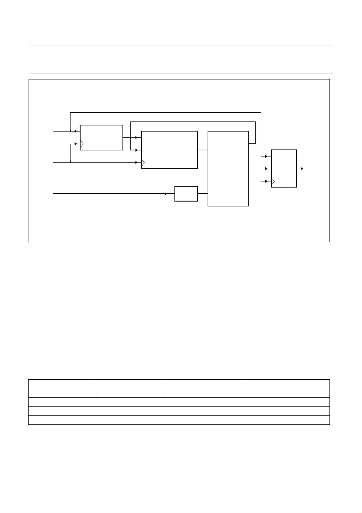
Philips Semiconductors Product specification
Microcontrollers for monitors with DDC
interface, auto-sync detection and sync proc.
handbook, full pagewidth
HSYNC_P
DIFFERENTIATOR
FOSH
Hper
R
8-BIT
E
COUNTER
Q7 to Q0
DIV 16
Fig.28 Vertical sync separator.
COMPARATOR
FOR
SYNC
SEPARATION
P83Cx80; P87C380
D
Vsep
Q
D-FF
E
MGG037
19.2.5 HORIZONTAL MODE DETECTION
This function block determines the following 4 parameters: Hper, Hpol, Hpres and Hcha. The functional block diagram is
shown in Fig.29.
The 12-bit counter for the determination of the horizontal period has a synchronous reset and will be reset by the
prescaled and differentiated horizontal pulse HSYNC_P, coming from the horizontal prescaler, or in case the counter
reaches the value FF0H as defined by the comparator. The latter situation will occur if no sync pulses are coming in or
if the frequency of the incoming sync pulses is too low.
The 12-bit register, that will store the 4 line time period, is only enabled if the signal HENA is HIGH.
19.2.5.1 Parameter Hper
Based on this configuration, the resulting accuracy for Hper will be:
×
Accuracy in H
=
------------------------------------------------------------------(horizontal counter value)
100%
100% f
=
-------------------------4FOSH×
H
Table 63 Accuracies
XTAL (f
(MHz)
clk
)
FOSH
(MHz)
ACCURACY IN H AT 30KHZ
(%)
ACCURACY IN V AT 50HZ
(%)
10 10 0.075 0.038
12 12 0.063 0.032
16 8 0.094 0.048
1997 Dec 12 58
Page 59

Philips Semiconductors Product specification
Microcontrollers for monitors with DDC
interface, auto-sync detection and sync proc.
A 12-bit counter is used to measure the frequency of
HSYNC. Every 4 HSYNC periods are measured and
compared with the previous locked HSYNC frequency; the
counter is reset every 4 HSYNC periods. The base clock
to the counter is for a 12 MHz system
1
------------------12 MHz
83 ns=
clock. If the new HSYNC frequency is larger than the
previous HSYNC frequency, there is a 4-bit counter to
avoid the noise or the temporary frequency shift.
When the 4-bit counter counts up to 15 for the comparison
Hfreq
(new)
> Hfreq
(previous)
, then the mode change interrupt
is issued. The time from mode change to interrupt issued
is approximately 4 × Hperiod
(4 × Hperiod
× 14)+n×Hperiod
(new)
(new)
× 15 or
(previous)
),
where n = 1, 2 or 3.
If the new HSYNC frequency is not in the static state and
is smaller than the previous HSYNC frequency, the time
from mode change to interrupt issued is approximately
(4 × Hperiod
× 3) − (n × Hperiod
(new)
(previous)
), where
n = 1, 2, 3 or 4. The static state is considered as the state
where the 12-bit counter, for measuring the HSYNC
frequency, reaches 4080.
For a 12 MHz system clock, the static state is equal to
1
--------------------------------83ns
×
4080
------------ 4
1
----------------------84660ns
11.8 kHz==
.
If the input HSYNC frequency is less than 11.8 kHz, it will
be regarded as static state. A 2-bit counter is used to avoid
the noise or the temporary shift.
When the new input HSYNC is changed to a static state,
the HSYNC frequency counter reaches 4080. In order to
have a faster response of the mode change interrupt, the
2-bit counter is not used and the mode change interrupt is
issued immediately. The time from mode change to
interrupt issued is approximately
((4080 + 5) × 83 ns) − (n × Hperiod
n = 1, 2, 3 or 4.
19.2.5.2 Parameter Hpres
The presence indicator Hpres, as stored in the SR flip-flop,
contains some hysteresis, as required due to the two
threshold settings in the comparator. The SR flip-flop will
be set, indicating that no active sync (or sync with a too low
frequency) is coming in if the counter reaches a value of
FF0H (4080 decimal). The corresponding horizontal sync
frequency is:
f
H
The SR flip-flop will be reset, indicating that an active sync
is present, if the counter reaches a value lower than FC0H
(4032 decimal). The corresponding horizontal sync
frequency is:
f
H
The hysteresis result,
Hysteresis Hfreq1 Hfreq2–()Hfreq1⁄=
is shown in Table 64.
P83Cx80; P87C380
(previous)
Hfreq1
== =
Hfreq2
== =
4 FOSH×
------------------------------------------- Counter value()
4 FOSH×
------------------------------------------- Counter value()
), where
4 FOSH×
--------------------------4080
4 FOSH×
--------------------------4032
,
When the 2-bit counter counts up to 3 for the comparison
‘static state’ < Hfreq
(new)
< Hfreq
(previous)
, then the mode
change interrupt is issued.
Table 64 Hysteresis in the Hpres detection
XTAL (f
(MHz)
clk
)
FOSH
(MHz)
Hfreq1
(MHz)
Hfreq2
(MHz)
10 10 9.804 9.921 1.2
12 12 11.765 11.905 1.2
16 8 7.843 7.937 1.2
1997 Dec 12 59
HYSTERESIS
(%)
Page 60

Philips Semiconductors Product specification
Microcontrollers for monitors with DDC
interface, auto-sync detection and sync proc.
19.2.5.3 Parameter Hpol
The mode change interrupt will be issued after 36 to 40
periods of the HSYNC when the polarity is changed from
negative to positive. The polarity indicator Hpol will be
changed from a logic 1 to a logic 0. The mode change
interrupt will be issued after the 60 periods of the HSYNC
when the polarity is changed from positive to negative. The
Hpol will be changed from a logic 0 to a logic 1. A logic 0
represents a positive polarity and a logic 1 represents a
negative polarity.
handbook, full pagewidth
Hres
HSYNC_P
RQ
FOSH
11 to Q0
12-BIT
COUNTER
D11 to D0
E
FOSH
19.2.5.4 Parameter Hcha
If Hcha is set to HIGH indicating that the period time has
changed for a long period, the Hper and Hpres will be
updated. If the measured period time has become stable
then the two counters will start to count down and the
HENA signal is set to LOW again, thereby disabling the
register Hper and the SR flip-flop for Hpres parameter.
Hcnt
12-BIT
REGISTER
Q11 to Q0
Hper
CHANGE
DETECTOR
P83Cx80; P87C380
HENA
Hlow
Hhgh
MODE
CHANGE
STABILIZATION
AND
COMPARISON
CIRCUIT
HSYNC
DIV 16
S
SR-FF
FOSH
R
D
D-FF
E
Hper and Hpol
DECISION
CIRCUIT
Fig.29 Horizontal mode detection.
Q
Q
Q
Hper
Hpres
Hpol
FOSH
Hcha
MGG038
1997 Dec 12 60
Page 61

Philips Semiconductors Product specification
Microcontrollers for monitors with DDC
interface, auto-sync detection and sync proc.
19.2.6 VERTICAL MODE DETECTION
To detect the vertical mode parameters Vper, Vpol and
Vpres, a circuit can be used which is almost similar to that
for the horizontal mode detection. The only difference is
that now the period time of one frame (instead of 4 lines)
is measured. The presence indication for the vertical sync
also contains a hysteresis of about 1.2%.
The formula to calculate the hysteresis is also similar to the
condition of HSYNC processing. A 12-bit counter is used
to count the clock number during one frame. Again FF0H
(4080 decimal) and FC0H (4032 decimal) are taken as the
threshold for Vfreq1 and Vfreq2 respectively, but the clock
FOSV = FOSH/76. Vfreq1, Vfreq2 and Hysteresis are
calculated as follows:
fVVfreq1
== =
f
Vfreq2
== =
V
FOSV
------------------------------------------- Counter value()
FOSV
------------------------------------------- Counter value()
FOSH
------------------------- 76 4080×
FOSH
------------------------- 76 4032×
The hysteresis result,
Hysteresis Vfreq1 Hfreq2–()Hfreq1⁄=
is shown in Table 64.
If the new VSYNC frequency is larger than the previous
VSYNC frequency, the time from mode change to interrupt
issued is approximately from
((Vperiod
If the new VSYNC frequency is not in the static state and
is smaller than the previous VSYNC frequency, the time
from mode change to interrupt issued is approximately
from Vperiod
frequency is in the static state, the time from mode change
to interrupt issued is approximately from
(4080 × 6.3 us) − Vperiod
× 2) + Vperiod
(new)
(new)
P83Cx80; P87C380
to Vperiod
(previous)
,
(previous)
(new)
) to (Vperiod
× 2. If the new VSYNC
to 4080 × 6.3 µs.
(new)
× 3).
Table 65 Hysteresis in the Vpres detection
(f
clk
(MHz)
)
FOSH
(MHz)
Vfreq1
(MHz)
Vfreq2
(MHz)
10 10 32.25 32.63 1.2
12 12 38.70 39.16 1.2
16 8 25.80 26.11 1.2
The polarity can be measured by looking to the level of the
input sync at1⁄4 of the frame time. The mode change in
vertical the frame period will be detected if there is a
change for a longer time than 3 frame periods.
The accuracy of Vper can calculated by the following
formula:
×
Accuracy in V
==
-----------------------------------------------------------(vertical counter value)
100% 76× f
=
---------------------------------------
100%
×
V
FOSH()
100% f
--------------------------
V
FOSV()
The hysteresis results and the accuracy of Vper are shown
in Table 63.
19.2.7 H
ORIZONTAL PULSE GENERATOR
Through the control flags, HPG1 and HPG0, the horizontal
pulse generator is able to generate the HSYNC
out
signal
with the following formats:
1. The same pulse as the input horizontal sync, or a
substitution pulse (with a fixed length) in case of a
2. A pulse starting at the beginning of the input horizontal
sync but now with a fixed length, or a substitution pulse
(with fixed length).
3. A free running sync pulse.
4. The same pulse as the input horizontal sync. The
substitution pulse is inhibited even if HSYNC is
missing.
To be able to generate a substitution pulse the down
counter, depicted in Fig.23, is loaded at each incoming
sync with a period time just a bit longer than the measured
Hper. If now normal syncs are present then the counter will
be loaded just before it reaches 000H. Therefore the
counter will not generate a pulse (in Fig.23, HPST remains
LOW). However, if a sync pulse is missing the counter will
reach 000H and generates a substitution pulse, HPST. At
the same time it will load itself again for the next run. To
generate free running pulses the only thing to do is to load
the down counter with the parameter HFP and to stop the
load pulses coming from the input sync, HSYNC_P. So,
the signal HPST is either a free running pulse or a pulse in
case an input sync is missing.
missing sync pulse.
HYSTERESIS
(%)
1997 Dec 12 61
Page 62

Philips Semiconductors Product specification
Microcontrollers for monitors with DDC
interface, auto-sync detection and sync proc.
The 5-bit down counter is used to generate a pulse with
pulse width t
. As shown in Fig.23, the SR flip-flop will
W(H)
be set by either HPST (free running/missing sync pulse) or
by the leading or trailing edge of the incoming sync pulse,
HSYNC_P. In the same way the SR flip-flop will be reset
by either the end of the incoming sync pulse or by the
pulse width counter.
handbook, full pagewidth
HSYNC_P
HFP
Hper
HPG1 to HPG0
DATA
LOAD
DECISION
PULSE
RISE/FALL
GENERATOR
If necessary (HPG1, HPG0: 1, 1), the substitution pulse
can be suppressed and only the incoming HSYNC pulse
will be delivered out. The frequency of the free running
pulse is:
The pulse width of the free running mode is:
t
W(H)=TFOSH
D9..0
L
FOSH
f
DOWN
COUNTER
Q
S
SR-FF
Q
R
FOSH
=
H(free)
----------------
× (HOPW<4:0>)
'0'
Q9..0
PHSI
P83Cx80; P87C380
Hfp
HPST
COMPARATOR
HSYNC
out
PULSE
HOPW
FOSH
WIDTH
GENERATOR
Fig.30 Horizontal pulse generator.
19.2.8 VERTICAL PULSE GENERATOR
The clock used in this vertical pulse generator must be
switchable between FOSV (needed to generate missing
sync pulses) and HPST (free running syncs from the
horizontal pulse generator) needed in the free running
mode. In the latter situation one vertical sync pulse (i.e.
one frame) will be generated by including an integer
number of the horizontal scanning lines (i.e. HPST). In this
case, the pulse width is also counted by HPST. The rest is
more or less equal to the horizontal pulse generator.
The frequency of the free running pulse is:
f
V(free)
-----------------2Vfp×
f
H(free)
=
The pulse width of the free running mode is:
t
W(V)=TH(free)
× [(VOPW<3:0>) + 2] × 2
MGG039
19.2.9 C
APTURE REGISTERS
This function captures the 6 parameters, Hper, Hpol,
Hpres, Vper, Vpol and Vpres such that the current value of
these parameters is available for the microcontroller core
(software) at all times. The mode change interrupt will be
activated if:
• The horizontal period changes
• The vertical period changes
• The horizontal polarity changes
• The vertical polarity changes.
19.2.10 C
ONTROL
All necessary control signals for the complete hardware
mode detection are mentioned in Section 19.1.
1997 Dec 12 62
Page 63

Philips Semiconductors Product specification
Microcontrollers for monitors with DDC
interface, auto-sync detection and sync proc.
19.2.11 THE DISPLAY PATTERN GENERATION
For certain events such as disconnection with the host or
the life test of monitor sets, it is convenient to have certain
display patterns shown on the monitor as the indication of
the operation of the monitor. The P83C880 provides two
simple patterns, the white pattern and the cross hatch
pattern for this purpose in the free running mode.
In the free running mode, the intervals of HSYNC and
VSYNC are determined by the 10-bit registers, HFP and
VFP. Based on the HFP and VFP, the internal down
counter will determine the starting or ending of the HSYNC
and VSYNC. The starting position, ending position and the
duration of the adjacent hatch lines are all related to the
programmed value of HFP and VFP. As a matter of fact,
the starting and ending position of the white pattern are
decided by the fixed number of FOSH clock and FOSV
clock (see Fig.31). Therefore, the position or dimension of
the white pattern is much related to HFP and VFP. The
duration of every two hatch lines (accordingly, the number
of hatch lines in the horizontal or vertical direction) will
depend on two fixed numbers (32, 32) which divide HFP
and VFP. For both white and cross hatch patterns, the
displayed pattern might look different in the different timing
modes and the symmetric display is not guaranteed.
However, they should be sufficient to be used as the
indicator to report the status of the monitor. Figure 31
demonstrates the display of the two patterns.
Two flags: PATENA (SFR PWME2) and PATTYP (SFR
PULCNT), are used to control the pattern display; for
detailed usage of those control bits refer to Section 7.3.6
and Section 19.1.9.
P83Cx80; P87C380
handbook, full pagewidth
32
HPST
16
HPST
32 FOSH 16 FOSH 32 FOSH
Fig.31 Two self test display patterns.
19.2.12 CLAMP OUTPUT
To facilitate the video processing in the following stage, the
clamping pulse can be delivered on pin
PWM8/CLAMP/P3.0 by setting flag CLMPEN (PULCNT.7)
to HIGH. The clamping pulse always accompanies the
HSYNC
pulse. Therefore, even in the free running mode
out
the clamping pulse is still present as long as the CLMPEN
bit is set. Flag FBPO (PULCNT.1) can be used to choose
the front porch clamp pulse (FBPO = 0) or the back porch
clamp pulse (FBPO = 1). The pulse width of the clamping
output signal is fixed to 8 FOSH clocks.
32 FOSH
2. THE CROSS HATCH1. THE WHITE PATTERN
16 FOSH
32
HPST
MGG040
The bit PHSI (PULCNT.0) is used to set the output polarity
of HSYNC
and the clamping pulse. If PHSI is LOW then
out
the output polarity will be positive, otherwise the output
polarity is negative.
1997 Dec 12 63
Page 64

Philips Semiconductors Product specification
Microcontrollers for monitors with DDC
interface, auto-sync detection and sync proc.
19.3 System operation
After a successful power-on reset, the P83C880 will
automatically start the mode detection and sync
separation by default. The output pulses of HSYNC and
VSYNC are delivered in the free running format by the
default setting. Since it takes at least 5 frames to finalize
the calculation of the HSYNC period, Hper, VSYNC period
and Vper, it is better to wait until the stable state is reached
to get the complete information after power-on reset.
Accordingly, Hpol, Vpol, Hpres, Vpres and sync separation
will be decided upon after Hper and Vper are settled. To
prevent interfering the CPU too often, the interrupt request
flag IE0 (SFR TCON) is only set if the mode (including
frequency or polarity) is changed. IE0 will be cleared either
by the CPU when the service routine is called (IT0 = 1) or
by the service routine itself (IT0 = 0).
If it is required to reduce power dissipation or if it is
preferred to stabilize the entire system after power-on
reset before mode detection is proceeded, the bit MARCH
(SFR MDCST) can be cleared to logic 0. Mode detection
can be activated at the desired moment later on by setting
MARCH to a logic 1.
In fact, the detection of the Device Power Management
Signalling (DPMS) modes like ‘Normal’, ‘Standby’,
‘Suspend’, ‘Power off’, etc. and sync separation are mixed
together with the display mode detection.
The mode detection function provides the hardware
vehicle to facilitate the mode detection and related
activities. Nevertheless, to use this facility to a maximum,
the proper interaction between software and hardware is
still essential. When VSYNC is absent and HSYNC is
present, the polarity of HSYNC is always fixed. A software
flow chart example is illustrated in Fig.32.
19.3.1 D
According to the DPMS specification: Hfreq <10 kHz and
Vfreq <10 Hz indicates that HSYNC and VSYNC are
inactive. However, in the real application, there are no
modes running with 10 kHz≤ Hfreq≤15 kHz and
10 Hz≤ Vfreq≤40 Hz. Therefore, Hfreq= 15 kHz and
Vfreq= 40 Hz are chosen as the threshold to indicate an
active or inactive signal for HSYNC and VSYNC
respectively.
P83Cx80; P87C380
ISPLAY POWER MANAGEMENT SIGNALLING
(DPMS) SPECIFICATION
1997 Dec 12 64
Page 65

Philips Semiconductors Product specification
Microcontrollers for monitors with DDC
interface, auto-sync detection and sync proc.
handbook, full pagewidth
IS Vpres = 1?
YES
NO
INTERRUPT OCCURS
IE0 IS SET
YES
IS Hpres = 1?
NO
IS Vpres = 1?
NO
P83Cx80; P87C380
YES
IS VSEL = 1?
YES
CHANGE VSEL = 0
NO
CHANGE VSEL = 1
RETURN
IF CSYNC IN?
(CHECK HSEL)
YES
SET HSEL = 0
SET VSEL = 0
NO
SET HSEL = 1
SET VSEL = 1
Fig.32 Software procedure in system operation: Mode detection flow chart.
MGG041
1997 Dec 12 65
Page 66

Philips Semiconductors Product specification
Microcontrollers for monitors with DDC
P83Cx80; P87C380
interface, auto-sync detection and sync proc.
20 POWER MANAGEMENT
The P83C880 supports power management. The
hardware mode detection complies to the Device Power
Management Signalling (DPMS) according to the
specification of VESA. The microcontroller is able to
distinguish between ‘Normal’, ‘Standby’, ‘Suspend’ and
‘Power off’ mode by detecting the frequency of HSYNC
and VSYNC. HSYNC is an active signal if its frequency is
above 15 kHz; otherwise, it is inactive. For VSYNC 40 Hz
is the threshold to judge if it is active or inactive. See also
Section 19.3.1. The exact values for the threshold depend
on the chosen crystal oscillator frequency:
10, 12 or 16 MHz.
The information about the status of HSYNC and VSYNC
can be represented by the bits, Hpres and Vpres in SFR
MDCST (address F8H).
Table 66 Display Power Management modes
OPERATING MODES HSYNC Hpres VSYNC Vpres
Normal active 1 active 1
Standby inactive 0 active 1
Suspend active 1 inactive 0
Power off inactive 0 inactive 0
The combination of Hpres and Vpres in relation to the
operating mode is shown in Table 66.
In the case of DDC2AB protocol, apart from hardware
mode detection, the protocol of ACCESS.bus also
supports Device Power Management Signalling (DPMS)
commands. In some operating modes the microcontroller
might enter a kind of power saving mode, i.e. Idle or
Power-down mode. In this situation the extremely low
retention voltage of 1.8 V for internal memory can support
the microcontroller to save its state before switching to Idle
or Power-down mode.
One set of I/O ports with the capability to drive LEDs can
help to highlight the current operating mode of monitors. It
is also possible to control the power consumption sources
like heater, main supply etc., through an I/O port in a
related operating mode.
21 CONTROL MODES
The microcontroller can operate in different control modes
(e.g. for emulation or OTP programming) by means of a
10-bit serial code that is shifted into the RESET input. The
signal at the XTAL1 pin serves as the shift clock.
The code is built up as follows: 0 XXXXX 0101; whereby
the first ‘0’ is the start bit, followed by a 5-bit code and
completed by ‘0101’. The 5-bit code determines the mode.
Normal mode is reached when no code is shifted in, but
the RESET pin remains HIGH for at least 10 cycles of the
XTAL1 input plus 20 µs.
When an OTP Programming/Verification, Emulation or a
Test mode should be entered, the timing must be as
shown in Fig.34.
The RESET signal is sampled on the rising edge of
XTAL1. Set-up and hold times for the RESET signal with
respect to the XTAL1 rising edge are 10 ns each.
The procedure to enter a specific control mode is as
follows:
1. Reset the microcontroller (CPU) by keeping the
RESET signal HIGH for at least 10 XTAL1 clock cycles
to escape any other control mode, plus at least 20 µs
(minimum of 24 internal clock cycles) to reset the
internal logic.
2. Shift in the specific code for the required control mode
(e.g. 011000 0101 for Emulation mode) via the
RESET pin and the XTAL1 clock (MSB first).
3. After the 10th bit the RESET signal should go LOW
within 9 cycles of XTAL1, otherwise the
microcontroller will enter Normal mode.
For the OTP Programming/Verification control modes see
Chapter 22.
1997 Dec 12 66
Page 67

Philips Semiconductors Product specification
Microcontrollers for monitors with DDC
interface, auto-sync detection and sync proc.
22 ONE TIME PROGRAMMABLE (OTP) VERSION
The OTP version P87C380 contains:
• 32 kbytes ROM
• 512 bytes RAM.
Next to the 32 kbytes ROM, another extra 384 bytes are
available. These bytes can be used for identification
purposes or to indicate the version number, etc. These
bytes are addressed via address lines A0 to A4.
Access to the OTP for program execution is done in
Normal mode. For writing and reading (Verification) of the
program memory and of the extra 384 bytes, different
control modes are used as shown in Table 67.
Table 68 Pin assignments during
Programming/Verification mode
PIN CONNECT TO
1V
2V
SS
SS
3 A13
4 A12
5A11
6 A10
7A9
8A8
9 XTAL1 (note 1)
10 XTAL2 (note 1)
11 V
12 V
DD
SS
13 WE
14 DI5/DO5
15 DI6/DO6
16
OE
17 DI4/DO4
18 A7
19 A6
20 A5
21 A4
22 A3
The signals and waveforms are given in Table 69 and
Fig.33. Pin connections to be used during Programming
and Verification are given in Table 68.
Table 67 Code for Programming/Verification of the
ROM: 32 kbytes (program memory) 010000 0101
Extra 384 bytes (memory) 0100010101
ROM: 32 kbytes (verification) 0111110101
Note
1. For driving the oscillator pins see Fig.10c.
P83Cx80; P87C380
OTP version P87C180A
MEMORY CODE
PIN CONNECT TO
23 A2
24 A1
25 A0
26 RESET
27 V
28 V
29 V
30 V
31 V
32 V
33 V
34 A14
35 V
36 DI3/DO3
37 DI2/DO2
38 DI1/DO1
39 DI0/DO0
40 DI7/DO7
41 V
42 V
SS
SS
SS
SS
SS
DD
SS
PP
SS
SS
1997 Dec 12 67
Page 68

Philips Semiconductors Product specification
Microcontrollers for monitors with DDC
P83Cx80; P87C380
interface, auto-sync detection and sync proc.
Table 69 Timing table for programming; see Fig.33
SYMBOL PARAMETER MIN. TYP. MAX. UNIT
t
su(AW)
t
h(AW)
t
su(AR)
t
h(AR)
t
su(D)
t
h(D)
t
su(prog)
t
h(prog)
t
W(prog)
t
W(R)
t
ACC(OE)
t
DZ(OE)
address set-up time write 2 −−µs
address hold time write 10 −−µs
address set-up time read 10 −−ns
address hold time read 200 −−ns
data set-up time 2 −−µs
data hold time 20 −−µs
programming voltage set-up time 10 −−µs
programming voltage hold time 10 −−µs
programming pulse width 90 −−µs
read pulse width 300 −−ns
output enable access verify 92 122 183 ns
data float after OE 10 −−ns
handbook, full pagewidth
address
A0 to A13
data in
DI0 to DI7
data out
DO0 to DO7
V
WE
PP
OE
10 µs
t
su(D)
10 µs
t
su(prog)
t
h(AW)
t
h(D)
t
su(AR)
t
ACC(OE)
t
h(prog)
t
h(AR)
DATA OUT VALID
t
W(R)
t
DZ(OE)
High Z
MGG051
V
IH
V
IL
t
V
IH
V
IL
V
IH
V
IL
V
IH
V
IL
V
PP
V
IL
V
IH
V
IL
su(AW)
ADDRESS VALID
DATA IN VALID
Fig.33 Programming waveforms.
1997 Dec 12 68
Page 69

Philips Semiconductors Product specification
Microcontrollers for monitors with DDC
interface, auto-sync detection and sync proc.
andbook, full pagewidth
RESET
93 XTAL1 CODE 5 XTAL1 4 XTAL1 4 XTAL1 8 XTAL1 4 XTAL1
XTAL1
Fig.34 Timing for OTP Programming/Verification.
23 LIMITING VALUES
In accordance with the Absolute Maximum Rating System (IEC 134).
x x x x x 00101
P83Cx80; P87C380
MBK517
SYMBOL PARAMETER MIN. MAX. UNIT
V
DD
V
I
I
source(max)
I
sink(max)
P
tot
T
stg
T
amb
supply voltage 4.4 5.5 V
input voltage (all inputs) −0.5 VDD+ 0.5 V
total maximum source current for all port lines 0.50 0.67 mA
total maximum sink current for all port lines 155 165 mA
total power dissipation 88.4 170 mW
storage temperature −60 +150 °C
operating ambient temperature (for all devices) −25 +85 °C
24 HANDLING
Inputs and outputs are protected against electrostatic discharge in normal handling. However, to be totally safe, it is
desirable to take normal precautions appropriate to handling MOS devices (see
“Handling MOS devices”
).
1997 Dec 12 69
Page 70

Philips Semiconductors Product specification
Microcontrollers for monitors with DDC
P83Cx80; P87C380
interface, auto-sync detection and sync proc.
25 DC CHARACTERISTICS
V
= 4.5 to 5.5 V; VSS=0V; T
DD
SYMBOL PARAMETER CONDITIONS MIN. TYP. MAX. UNIT
Supply
V
I
V
DD
DD
POR
operating supply voltage 4.4 5 5.5 V
operating supply current f
Power-on-reset voltage level 3.6 3.9 4.2 V
PROGRAMMING SUPPLY
V
DD(P)
V
PP
I
DD(P)
I
PP
supply voltage programming mode 4.4 5.0 5.5 V
programming voltage 12.0 12.75 13.0 V
supply current programming mode 10.6 19.1 24.0 mA
programming current 77.8 80.1 81.3 mA
RESET
R
I(RESET)
I
LI
V
IL
V
IH
HSYNC
I
IL
V
IL
V
IH
CSYNC
I
LI
V
IL
V
IH
I
OL
I
OH
input resistance RESET VDD= 4.5 V to 5.5 V 20 60 180 kΩ
input leakage current VSS<VI<V
LOW-level input voltage VSS− 0.5 − 0.3V
HIGH-level input voltage 0.7V
/PROG and VSYNCin/OE
in
Input leakage current VSS<VI<V
LOW-level input voltage VSS− 0.5 − 0.8 V
HIGH-level input voltage 2.0 − VDD+ 0.5 V
/P1.6
in
input leakage current VSS<VI<V
LOW-level input voltage VSS− 0.5 − 0.8 V
HIGH-level input voltage 2.0 − VDD+ 0.5 V
LOW-level output sink current VO≤ 0.4 V 1.6 −− mA
HIGH-level pull-up output source
current
strong pull-up during 2 clock
cycles
weak pull-up V
Port 0
V
IL
V
IH
I
LI
I
IT
I
OL
LOW-level input voltage VSS− 0.5 − 0.3V
HIGH-level input voltage 0.7V
input leakage current VI= 0.4VDD; VDD=5V −10 −−100 µA
input transition current VI= 0.5VDD; VDD=5V −−−1000 µA
LOW-level output sink current VO≤ 0.4 V 1.6 −− mA
= −25 to +85 °C; all voltages with respect to VSS unless otherwise specified.
amb
= 12 MHz 20.1 29.4 30.9 mA
clk
f
= 16 MHz 25.2 36.1 38.4 mA
clk
DD
DD
DD
DD
≤ 1.0 V 10 −− mA
V
O
V
O=VDD
O=VDD
V
O
− 0.4 V 1.6 −− mA
− 0.4 V 25 −− µA
DD
≤ 1.0 V 10 −− mA
− VDD+ 0.5 V
− VDD+ 0.5 V
±10 µA
−10 µA
−10 µA
DD
DD
V
V
1997 Dec 12 70
Page 71

Philips Semiconductors Product specification
Microcontrollers for monitors with DDC
P83Cx80; P87C380
interface, auto-sync detection and sync proc.
SYMBOL PARAMETER CONDITIONS MIN. TYP. MAX. UNIT
I
OH
Port 1: SCL/P1.0, SDA/P1.1, SCL1/P1.2 and SDA1/P1.3
V
IL
V
IH
I
LI
I
IT
I
OL
I
OH
Port 1 and 3: VSYNC
V
IL
V
IH
I
LI
I
IT
I
OL
I
OH
Port 2 and 3: P2.0/PWM0 to P2.7/PWM7 and Port P3.0/PWM8/CLAMP to P3.1/PWM9/PATOUT
V
IL
V
IH
I
LI
I
IT
I
OL
I
OH
HIGH-level pull-up output source
current
strong pull-up during 2 clock
V
O=VDD
− 0.4 V 1.6 −− mA
cycles
weak pull-up V
O=VDD
LOW-level input voltage VSS− 0.5 − 0.3V
HIGH-level input voltage 0.7V
− 0.4 V 25 −− µA
V
DD
DD
− VDD+ 0.5 V
input leakage current VI= 0.4VDD; VDD=5V −10 −−100 µA
input transition current VI= 0.5VDD; VDD=5V −−−1000 µA
LOW-level output sink current VO= 0.4 V; VDD= 5V 3.0 −− mA
HIGH-level pull-up output source
current
strong pull-up during 2 clock
V
O=VDD
− 0.4 V 1.6 −− mA
cycles
weak pull-up V
/P1.4, HSYNC
out
/P1.5, PWM10/P1.7 and ADC0/P3.2 to ADC1/P3.3
out
O=VDD
LOW-level input voltage VSS− 0.5 − 0.3V
HIGH-level input voltage 0.7V
− 0.4 V 25 −− µA
V
DD
DD
− VDD+ 0.5 V
input leakage current VI= 0.4VDD; VDD=5V −10 −−100 µA
input transition current VI= 0.5VDD; VDD=5V −−−1000 µA
LOW-level output sink current VO≤ 0.4 V 1.6 −− mA
HIGH-level pull-up output source
current
strong pull-up during 2 clock
V
O=VDD
− 0.4 V 1.6 −− mA
cycles
weak pull-up V
O=VDD
− 0.4 V 25 −− µA
1997 Dec 12 71
Page 72

Philips Semiconductors Product specification
Microcontrollers for monitors with DDC
P83Cx80; P87C380
interface, auto-sync detection and sync proc.
SYMBOL PARAMETER CONDITIONS MIN. TYP. MAX. UNIT
INT1/V
PP
V
IL
V
IH
V
− VDDinput voltage with respect to V
IH
Note
1. This maximum applies at all times, including during power switching, and must be accounted for in power supply
design. During a power-on process, the +12 V source used for external pull-up resistors should not precede the V
of the P83C880, P83C180, P83C280 and P83C380 up their respective voltage ramps by more than this margin, nor,
during a power-down process, should VDD precede +12 V down their respective voltage ramps by more than this
margin.
26 DIGITAL-TO-ANALOG CONVERTER CHARACTERISTICS
=5V; V
V
DD
SYMBOL PARAMETER TEST CONDITION MIN. TYP. MAX. UNIT
V
DD
RES
I
o(DAC)
I
o(DAC)(id)
V
o(DAC)
DL
e
t
st
∆V
o(T)
∆V
o
LOW-level input voltage VSS− 0.5 − 0.2VDD− 0.1 V
HIGH-level input voltage IIH= 2 mA 0.2VDD+ 0.9 − 12.6 V
−−8V
DDA
=5V; T
amb
DD
=27°C.
supply voltage 4.4 − 5.5 V
DAC
DAC resolution − 8 − bit
operating current for each
DAC channel
DAC idle current all 4 DAC channels
output pin connected to
V
via 40 kΩ
DDA
−−2.5 mA
−−61 µA
shut-down
DAC output level voltage output pin open 0 − V
at FFH code input;
I
= −1mA (note 1)
OH
at 00H code input;
I
= 1mA
OL
V
− 0.2 −−V
DDA
−−0.2 V
differential non-linearity output level 0.2 to 4.8 V −1 − +1 LSB
settling time −−20 ms
output voltage variation
−−1.5 mV/°C
due to temperature drift
output voltage ripple T
>20ms −−2mV
test
DDA
V
DD
Note
1. The ‘negative’ value denotes that the current is sourcing out from the chip into the load device through the output pin.
1997 Dec 12 72
Page 73

Philips Semiconductors Product specification
Microcontrollers for monitors with DDC
P83Cx80; P87C380
interface, auto-sync detection and sync proc.
27 AC CHARACTERISTICS
V
= 4.5 V to 5.5 V; VSS=0V; T
DD
SYMBOL PARAMETER CONDITIONS MIN. TYP. MAX. UNIT
f
clk
f
PXE
C
XTAL1
crystal oscillator frequency VDD=5V 101216MHz
PXE resonator frequency VDD= 5 V 10 12 16 MHz
external capacitance at XTAL1
with crystal resonator − 20 27 pF
with PXE resonator − 20 27 pF
C
XTAL2
external capacitance at XTAL2
with crystal resonator − 20 27 pF
with PXE resonator − 20 27 pF
Analog-to-Digital Converter (software)
V
in(A)
comparator analog input voltages
ADC0; ADC1
V
AE
t
conv(ADC)
conversion error range −−±
conversion time (from any change in
ADC input i.e. voltage level)
DDC1 Mode
t
DOV
t
VCLKH
t
VCLKL
t
t(mode)
t
sup(input)
(1)
(transmit-only, unidirectional); see Figs 25 and 35
output valid from VCLK −−30 µs
VCLK high time 20 −−µs
VCLK low time 20 −−µs
mode transition time −−800 ns
input filter spike suppression; for SDA,
SCL and VSYNC
t
su(DDC1)
DDC1 mode set-up time − 5 −µs
Horizontal sync input for the mode detection; see Fig.36
Hfreq HSYNC input frequency 15 − 150 kHz
t
W(HSYNC)
H
DCYC
t
ir(HSYNC)
t
if(HSYNC)
HSYNC input pulse width notes 2 and 3 0.25 − 8 µs
HSYNC input duty cycle notes 2 and 3 −−25 %
HSYNC input rise time −−100 ns
HSYNC input fall time −−100 ns
Vertical Sync Input for the Mode Detection; see Fig.37
Vfreq VSYNC input frequency 40 − 200 Hz
t
W(VSYNC)
V
DCYC
t
ir(VSYNC)
t
if(VSYNC)
VSYNC input pulse width note 4 1 − 24 note 5
VSYNC input duty cycle note 4 −−25 %
VSYNC input rise time −−100 ns
VSYNC input fall time −−100 ns
= −25 to + 85 °C; all voltages with respect to VSS unless otherwise specified.
amb
V
SS
− V
DD
1
−−7µs
−−200 ns
⁄
2
V
LSB
1997 Dec 12 73
Page 74
Philips Semiconductors Product specification
Microcontrollers for monitors with DDC
P83Cx80; P87C380
interface, auto-sync detection and sync proc.
SYMBOL PARAMETER CONDITIONS MIN. TYP. MAX. UNIT
Composite Sync Input for the Mode Detection; see Figs 38 and 39
T
EQ(CSYNC)
equalizing pulse period for CSYNC
input
t
WEQ(CSYNC)
equalizing pulse width for CSYNC
input
NEQ equalizing pulses plus the VSYNC
interval
Horizontal and Vertical Pulse Generation; see Figs 40 and 41
T
H(free)
t
WH(free)
t
or(HSYNC)
t
of(HSYNC)
t
d(in-out)(HSYNC)
t
dmax(HSYNCm)
horizontal pulse period in free running 10 − 66 µs
horizontal pulse width in free running 0.4 − 2.5 µs
HSYNC output pulse rise time 30 31 32 ns
HSYNC output pulse fall time 24 26 28 ns
HSYNC output delay to input −−100 ns
HSYNC output maximum delay after
missing HSYNC
t
W(HSYNCsub)
t
d(HSYNC-CLAMP)
t
W(CLAMP)
T
V(free)
t
WV(free)
t
or(VSYNC)
t
of(VSYNC)
t
d(in-out)(VSYNC)
t
dmax(VSYNCm)
HSYNC output substitution pulse width −−2.5 µs
CLAMP pulse delay to HSYNC input 0−125 ns
CLAMP pulse width 0.4 − 2.5 µs
vertical pulse period in free running −−2048 note 5
vertical pulse width in free running −−32 note 5
VSYNC output pulse rise time 22 24 26 ns
VSYNC output pulse fall time 24 27 30 ns
VSYNC output delay to input −−250 ns
VSYNC output maximum delay after
missing VSYNC
t
W(VSYNCsub)
VSYNC output substitution pulse width −−16 note 5
Slope control port
t
tLH(sce)
LOW-to-HIGH transition delay while
0.1VDDto 0.9VDD; note 7 25 − 100 ns
slope control enabled
t
tHL(sce)
HIGH-to-LOW transition delay while
0.9VDDto 0.1VDD; note 7 25 − 100 ns
slope control enabled
t
PLH(scd)
t
PHL(scd)
LOW-to-HIGH propagation delay while
slope control disabled
HIGH-to-LOW propagation delay while
slope control disabled
0.1VDDto 0.9VDD;
load = 50 pF
0.9VDDto 0.1VDD;
load = 50 pF
− 0.5 − note 5
− 0.5 − note 6
−−30 note 5
−−350 ns
−−1 note 5
−−10 ns
−−10 ns
Notes
1. For the DDC2 Mode (bidirectional I2C-bus mode), refer to the standard I2C-bus specification.
2. The actual sync width has to fulfil both requirements, maximum pulse width t
cycle H
of 25%, at the same time.
DCYC
W(HSYNC)
= 8.0 µs and maximum duty
3. The polarity of the horizontal sync pulse is said to be positive if the HIGH period is shorter than the LOW period.
4. The actual sync width has to fulfil both requirements, maximum pulse width t
and maximum duty cycle V
of 25%, at the same time.
DCYC
W(VSYNC)
= 24 horizontal line periods
1997 Dec 12 74
Page 75

Philips Semiconductors Product specification
Microcontrollers for monitors with DDC
interface, auto-sync detection and sync proc.
5. Unit is HSYNC line period: T
6. Unit is HSYNC pulse width: t
7. This transition delay has to be loaded independent for capacitances up to 50 pF.
handbook, full pagewidth
SCL
SDA
VCLK
line(HSYNC).
W(HSYNC)
transmit only mode
t
t(mode)
.
(DDC1)
bidirectional mode
(DDC2)
P83Cx80; P87C380
handbook, full pagewidth
HSYNC
t
if(HSYNC)
handbook, full pagewidth
VSYNC
t
W(HSYNC)
H
DCYC
Fig.35 Mode transition from DDC1 to DDC2.
t
ir(HSYNC)
T
HSYNC
Fig.36 Horizontal sync input signal.
MGG052
MGG053
t
t
if(VSYNC)
W(VSYNC)
V
DCYC
t
ir(VSYNC)
T
VSYNC
Fig.37 Vertical sync input signal.
1997 Dec 12 75
MGG054
Page 76

Philips Semiconductors Product specification
Microcontrollers for monitors with DDC
interface, auto-sync detection and sync proc.
handbook, full pagewidth
CSYNC
HSYNC
VSYNC
CSYNC
t
W(CSYNC)
2nd field 1st field
t
WEQ(CSYNC)
T
EQ(CSYNC)
NEQ
P83Cx80; P87C380
1/H
freq
HSYNC
VSYNC
2nd field 1st field
Fig.38 Standard composite sync pulse wave forms.
MGG055
1997 Dec 12 76
Page 77
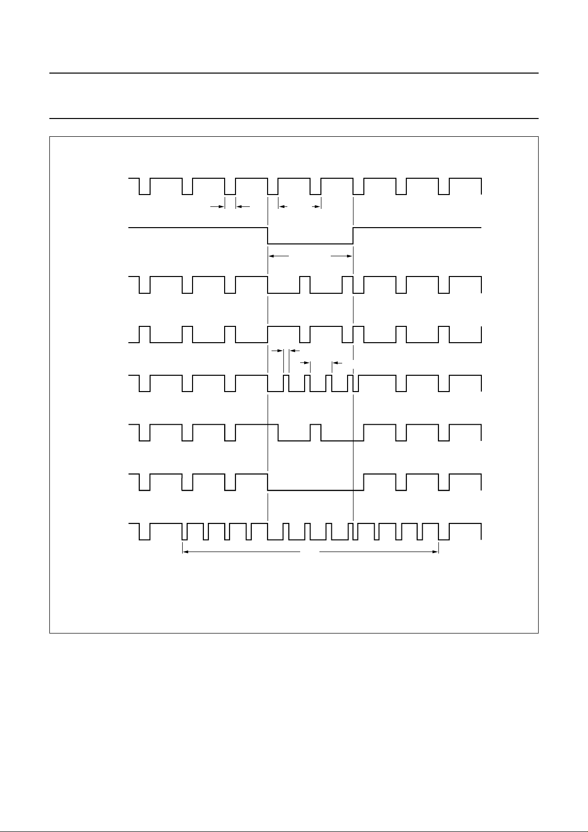
Philips Semiconductors Product specification
Microcontrollers for monitors with DDC
interface, auto-sync detection and sync proc.
handbook, full pagewidth
HSYNC
VSYNC
CSYNC-1
CSYNC-2
t
W(HSYNC)
1/H
freq
t
W(VSYNC)
t
WEQ(CSYNC)
T
EQ(CSYNC)
P83Cx80; P87C380
CSYNC-3
CSYNC-4
CSYNC-5
CSYNC-6
NEQ
Fig.39 Composite sync pulse wave forms.
MGG056
1997 Dec 12 77
Page 78
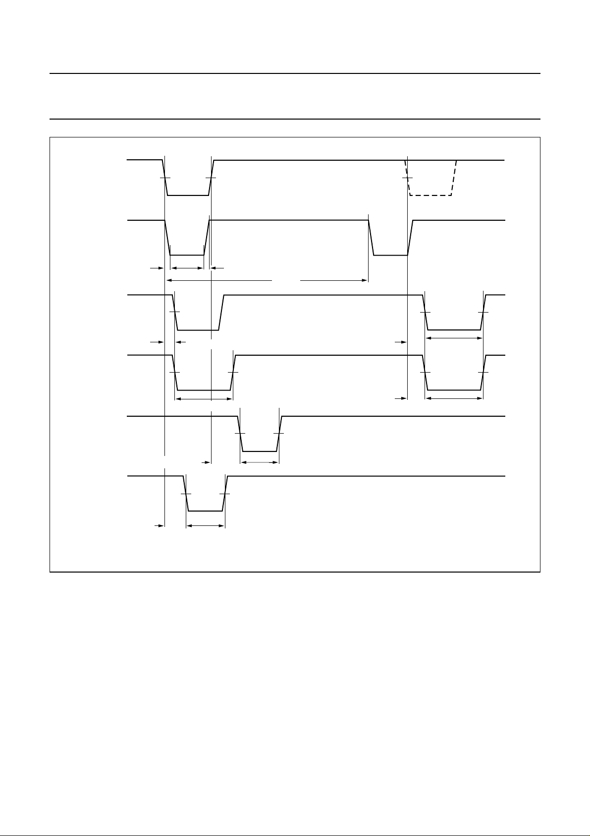
Philips Semiconductors Product specification
Microcontrollers for monitors with DDC
interface, auto-sync detection and sync proc.
handbook, full pagewidth
HSYNC
HSYNC
out
(free running)
t
of(HSYNC)
HSYNC
out
(sync/
substitution)
HSYNC
out
(sync/substitution
with fixed pulse
width)
t
WH(free)
t
d(in-out)(HSYNC)
t
W(HSYNCsub)
t
or(HSYNC)
T
H(free)
t
dmax(HSYNCm)
t
dmax(HSYNCm)
P83Cx80; P87C380
t
W(HSYNCsub)
t
W(HSYNCsub)
CLAMP
(clamp pulse
at back porch)
CLAMP
(clamp pulse
at front porch)
t
d(HSYNC-CLAMP)
t
d(HSYNC-CLAMP)
t
W(CLAMP)
t
W(CLAMP)
Fig.40 Horizontal sync output pulse.
MGG057
1997 Dec 12 78
Page 79
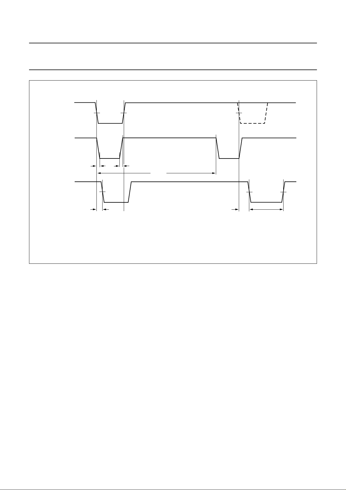
Philips Semiconductors Product specification
Microcontrollers for monitors with DDC
interface, auto-sync detection and sync proc.
handbook, full pagewidth
VSYNC
VSYNC
out
(free running)
t
or(VSYNC)
T
V(free)
VSYNC
out
(sync/
substitution)
t
of(VSYNC)
t
WV(free)
t
d(in-out)(VSYNC)
t
dmax(VSYNCm)
P83Cx80; P87C380
t
W(VSYNCsub)
MGG058
Fig.41 Vertical sync output pulse.
1997 Dec 12 79
Page 80

Philips Semiconductors Product specification
Microcontrollers for monitors with DDC
interface, auto-sync detection and sync proc.
28 PACKAGE OUTLINE
SDIP42: plastic shrink dual in-line package; 42 leads (600 mil)
D
seating plane
L
Z
e
P83Cx80; P87C380
SOT270-1
M
E
A
2
A
A
1
w M
b
1
c
(e )
M
1
H
42
pin 1 index
1
DIMENSIONS (mm are the original dimensions)
A
A
A
UNIT b
max.
mm
5.08 0.51 4.0
12
min.
max.
b
1.3
0.8
0.53
0.40
b
22
E
21
0 5 10 mm
scale
cEe M
1
0.32
0.23
(1) (1)
D
38.9
38.4
14.0
13.7
1
L
M
E
3.2
15.80
2.9
15.24
17.15
15.90
e
w
H
0.181.778 15.24
Z
max.
1.73
(1)
Note
1. Plastic or metal protrusions of 0.25 mm maximum per side are not included.
OUTLINE
VERSION
SOT270-1
IEC JEDEC EIAJ
REFERENCES
1997 Dec 12 80
EUROPEAN
PROJECTION
ISSUE DATE
90-02-13
95-02-04
Page 81

Philips Semiconductors Product specification
Microcontrollers for monitors with DDC
interface, auto-sync detection and sync proc.
29 SOLDERING
29.1 Introduction
There is no soldering method that is ideal for all IC
packages. Wave soldering is often preferred when
through-hole and surface mounted components are mixed
on one printed-circuit board. However, wave soldering is
not always suitable for surface mounted ICs, or for
printed-circuits with high population densities. In these
situations reflow soldering is often used.
This text gives a very brief insight to a complex technology.
A more in-depth account of soldering ICs can be found in
our
“IC Package Databook”
29.2 Soldering by dipping or by wave
The maximum permissible temperature of the solder is
260 °C; solder at this temperature must not be in contact
with the joint for more than 5 seconds. The total contact
time of successive solder waves must not exceed
5 seconds.
(order code 9398 652 90011).
The device may be mounted up to the seating plane, but
the temperature of the plastic body must not exceed the
specified maximum storage temperature (T
printed-circuit board has been pre-heated, forced cooling
may be necessary immediately after soldering to keep the
temperature within the permissible limit.
29.3 Repairing soldered joints
Apply a low voltage soldering iron (less than 24 V) to the
lead(s) of the package, below the seating plane or not
more than 2 mm above it. If the temperature of the
soldering iron bit is less than 300 °C it may remain in
contact for up to 10 seconds. If the bit temperature is
between 300 and 400 °C, contact may be up to 5 seconds.
P83Cx80; P87C380
). If the
stg max
1997 Dec 12 81
Page 82

Philips Semiconductors Product specification
Microcontrollers for monitors with DDC
P83Cx80; P87C380
interface, auto-sync detection and sync proc.
30 DEFINITIONS
Data sheet status
Objective specification This data sheet contains target or goal specifications for product development.
Preliminary specification This data sheet contains preliminary data; supplementary data may be published later.
Product specification This data sheet contains final product specifications.
Limiting values
Limiting values given are in accordance with the Absolute Maximum Rating System (IEC 134). Stress above one or
more of the limiting values may cause permanent damage to the device. These are stress ratings only and operation
of the device at these or at any other conditions above those given in the Characteristics sections of the specification
is not implied. Exposure to limiting values for extended periods may affect device reliability.
Application information
Where application information is given, it is advisory and does not form part of the specification.
31 LIFE SUPPORT APPLICATIONS
These products are not designed for use in life support appliances, devices, or systems where malfunction of these
products can reasonably be expected to result in personal injury. Philips customers using or selling these products for
use in such applications do so at their own risk and agree to fully indemnify Philips for any damages resulting from such
improper use or sale.
32 PURCHASE OF PHILIPS I
Purchase of Philips I
components in the I2C system provided the system conforms to the I2C specification defined by
Philips. This specification can be ordered using the code 9398 393 40011.
2
C COMPONENTS
2
C components conveys a license under the Philips’ I2C patent to use the
1997 Dec 12 82
Page 83

Philips Semiconductors Product specification
Microcontrollers for monitors with DDC
interface, auto-sync detection and sync proc.
NOTES
P83Cx80; P87C380
1997 Dec 12 83
Page 84

Philips Semiconductors – a worldwide company
Argentina: see South America
Australia: 34 Waterloo Road, NORTH RYDE, NSW 2113,
Tel. +61 2 9805 4455, Fax. +61 2 9805 4466
Austria: Computerstr. 6, A-1101 WIEN, P.O. Box 213, Tel. +43 160 1010,
Fax. +43 160 101 1210
Belarus: Hotel Minsk Business Center, Bld. 3, r. 1211, Volodarski Str. 6,
220050 MINSK, Tel. +375 172 200 733, Fax. +375 172 200 773
Belgium: see The Netherlands
Brazil: see South America
Bulgaria: Philips Bulgaria Ltd., Energoproject, 15th floor,
51 James Bourchier Blvd., 1407 SOFIA,
Tel. +359 2 689 211, Fax. +359 2 689 102
Canada: PHILIPS SEMICONDUCTORS/COMPONENTS,
Tel. +1 800 234 7381
China/Hong Kong: 501 Hong Kong Industrial Technology Centre,
72 Tat Chee Avenue, Kowloon Tong, HONG KONG,
Tel. +852 2319 7888, Fax. +852 2319 7700
Colombia: see South America
Czech Republic: see Austria
Denmark: Prags Boulevard 80, PB 1919, DK-2300 COPENHAGEN S,
Tel. +45 32 88 2636, Fax. +45 31 57 0044
Finland: Sinikalliontie 3, FIN-02630 ESPOO,
Tel. +358 9 615800, Fax. +358 9 61580920
France: 51 Rue Carnot, BP317, 92156 SURESNES Cedex,
Tel. +33 1 40 99 6161, Fax. +33 1 40 99 6427
Germany: Hammerbrookstraße 69, D-20097 HAMBURG,
Tel. +49 40 23 53 60, Fax. +49 40 23 536 300
Greece: No. 15, 25th March Street, GR 17778 TAVROS/ATHENS,
Tel. +30 1 4894 339/239, Fax. +30 1 4814 240
Hungary: see Austria
India: Philips INDIA Ltd, Band Box Building, 2nd floor,
254-D, Dr. Annie Besant Road, Worli, MUMBAI 400 025,
Tel. +91 22 493 8541, Fax. +91 22 493 0966
Indonesia: see Singapore
Ireland: Newstead, Clonskeagh, DUBLIN 14,
Tel. +353 1 7640 000, Fax. +353 1 7640 200
Israel: RAPAC Electronics, 7 Kehilat Saloniki St, PO Box 18053,
TEL AVIV 61180, Tel. +972 3 645 0444, Fax. +972 3 649 1007
Italy: PHILIPS SEMICONDUCTORS, Piazza IV Novembre 3,
20124 MILANO, Tel. +39 2 6752 2531, Fax. +39 2 6752 2557
Japan: Philips Bldg 13-37, Kohnan 2-chome, Minato-ku, TOKYO 108,
Tel. +81 3 3740 5130, Fax. +81 3 3740 5077
Korea: Philips House, 260-199 Itaewon-dong, Yongsan-ku, SEOUL,
Tel. +82 2 709 1412, Fax. +82 2 709 1415
Malaysia: No. 76 Jalan Universiti, 46200 PETALING JAYA, SELANGOR,
Tel. +60 3 750 5214, Fax. +60 3 757 4880
Mexico: 5900 Gateway East, Suite 200, EL PASO, TEXAS 79905,
Tel. +9-5 800 234 7381
Middle East: see Italy
Netherlands: Postbus 90050, 5600 PB EINDHOVEN, Bldg. VB,
Tel. +31 40 27 82785, Fax. +31 40 27 88399
New Zealand: 2 Wagener Place, C.P.O. Box 1041, AUCKLAND,
Tel. +64 9 849 4160, Fax. +64 9 849 7811
Norway: Box 1, Manglerud 0612, OSLO,
Tel. +47 22 74 8000, Fax. +47 22 74 8341
Philippines: Philips Semiconductors Philippines Inc.,
106 Valero St. Salcedo Village, P.O. Box 2108 MCC, MAKATI,
Metro MANILA, Tel. +63 2 816 6380, Fax. +63 2 817 3474
Poland: Ul. Lukiska 10, PL 04-123 WARSZAWA,
Tel. +48 22 612 2831, Fax. +48 22 612 2327
Portugal: see Spain
Romania: see Italy
Russia: Philips Russia, Ul. Usatcheva 35A, 119048 MOSCOW,
Tel. +7 095 755 6918, Fax. +7 095 755 6919
Singapore: Lorong 1, Toa Payoh, SINGAPORE 1231,
Tel. +65 350 2538, Fax. +65 251 6500
Slovakia: see Austria
Slovenia: see Italy
South Africa: S.A. PHILIPS Pty Ltd., 195-215 Main Road Martindale,
2092 JOHANNESBURG, P.O. Box 7430 Johannesburg 2000,
Tel. +27 11 470 5911, Fax. +27 11 470 5494
South America: Al. Vicente Pinzon, 173, 6th floor,
04547-130 SÃO PAULO, SP, Brazil,
Tel. +55 11 821 2333, Fax. +55 11 821 2382
Spain: Balmes 22, 08007 BARCELONA,
Tel. +34 3 301 6312, Fax. +34 3 301 4107
Sweden: Kottbygatan 7, Akalla, S-16485 STOCKHOLM,
Tel. +46 8 632 2000, Fax. +46 8 632 2745
Switzerland: Allmendstrasse 140, CH-8027 ZÜRICH,
Tel. +41 1 488 2686, Fax. +41 1 481 7730
Taiwan: Philips Semiconductors, 6F, No. 96, Chien Kuo N. Rd., Sec. 1,
TAIPEI, Taiwan Tel. +886 2 2134 2865, Fax. +886 2 2134 2874
Thailand: PHILIPS ELECTRONICS (THAILAND) Ltd.,
209/2 Sanpavuth-Bangna Road Prakanong, BANGKOK 10260,
Tel. +66 2 745 4090, Fax. +66 2 398 0793
Turkey: Talatpasa Cad. No. 5, 80640 GÜLTEPE/ISTANBUL,
Tel. +90 212 279 2770, Fax. +90 212 282 6707
Ukraine: PHILIPS UKRAINE, 4 Patrice Lumumba str., Building B, Floor 7,
252042 KIEV, Tel. +380 44 264 2776, Fax. +380 44 268 0461
United Kingdom: Philips Semiconductors Ltd., 276 Bath Road, Hayes,
MIDDLESEX UB3 5BX, Tel. +44 181 730 5000, Fax. +44 181 754 8421
United States: 811 East Arques Avenue, SUNNYVALE, CA 94088-3409,
Tel. +1 800 234 7381
Uruguay: see South America
Vietnam: see Singapore
Yugoslavia: PHILIPS, Trg N. Pasica 5/v, 11000 BEOGRAD,
Tel. +381 11 625 344, Fax.+381 11 635 777
For all other countries apply to: Philips Semiconductors,
International Marketing & Sales Communications, Building BE-p,
P.O. Box 218, 5600 MD EINDHOVEN, The Netherlands, Fax. +31 40 27 24825
© Philips Electronics N.V. 1997 SCA56
All rights are reserved. Reproduction in whole or in part is prohibited without the prior written consent of the copyright owner.
The information presented in this document does not form part of any quotation or contract, is believed to be accurate and reliable and may be changed
without notice. No liability will be accepted by the publisher for any consequence of its use. Publication thereof does not convey nor imply any license
under patent- or other industrial or intellectual property rights.
Internet: http://www.semiconductors.philips.com
Printed in The Netherlands 457041/1200/01/pp84 Date of release: 1997 Dec 12 Document order number: 9397 750 03171
 Loading...