

Philips P80C562EBA-02, P80C562EFA-02, P80C562EHA-02 Datasheet

DATA SH EET
Product specification
File under Integrated Circuits, IC20
1997 Apr 16
INTEGRATED CIRCUITS
P83C562; P80C562
8-bit microcontroller

1997 Apr 08 2
Philips Semiconductors Product specification
8-bit microcontroller P83C562; P80C562
CONTENTS
1 FEATURES
2 GENERAL DESCRIPTION
3 ORDERING INFORMATION
4 BLOCK DIAGRAM
5 FUNCTIONAL DIAGRAM
6 PINNING INFORMATION
6.1 Pinning
6.2 Pin description
7 FUNCTIONAL DESCRIPTION
8 MEMORY ORGANIZATION
8.1 Program Memory
8.2 Addressing
9 I/O FACILITIES
10 PULSE WIDTH MODULATED OUTPUTS
10.1 Prescaler Frequency Control Register (PWMP)
10.2 Pulse Width Register 0 (PWM0)
10.3 Pulse Width Register 1 (PWM1)
11 ANALOG-TO-DIGITAL CONVERTER (ADC)
11.1 Analog input pins
11.2 ADC Control Register (ADCON)
12 TIMER/ COUNTERS
12.1 Timer 0 and Timer 1
12.2 Timer T2 Capture and Compare Logic
12.2.1 T2 Control Register (TM2CON)
12.2.2 Capture Control Register (CTCON)
12.2.3 Interrupt Flag Register (TM2IR)
12.2.4 Set Enable Register (STE)
12.2.5 Reset/Toggle Enable register (RTE)
12.3 Watchdog Timer (T3)
13 SERIAL I/O
14 INTERRUPT SYSTEM
14.1 Interrupt Vectors
14.2 Interrupt priority
14.3 Interrupt Enable and Priority Registers
14.3.1 Interrupt Enable Register 0 (IEN0)
14.3.2 Interrupt Enable register 1 (IEN1)
14.3.3 Interrupt priority register 0 (IP0)
14.3.4 Interrupt Priority Register 1 (IP1)
15 REDUCED POWER MODES
15.1 Idle and Power-down operation
15.1.1 Idle mode
15.1.2 Power-down mode
15.2 Power Control Register (PCON)
16 OSCILLATOR CIRCUITRY
17 RESET CIRCUITRY
17.1 Power-on-reset
18 INSTRUCTION SET
19 LIMITING VALUES
20 DC CHARACTERISTICS
21 AC CHARACTERISTICS
22 PACKAGE OUTLINES
23 SOLDERING
23.1 Introduction
23.2 Reflow soldering
23.3 Wave soldering
23.4 Repairing soldered joints
24 DEFINITIONS
25 LIFE SUPPORT APPLICATIONS

1997 Apr 08 3
Philips Semiconductors Product specification
8-bit microcontroller P83C562; P80C562
1 FEATURES
• 80C51 Central Processing Unit
• 8 kbytes ROM, expandable externally to 64 kbytes
• 256 bytes RAM, expandable externally to 64 kbytes
• Two standard 16-bit timer/counters
• An additional 16-bit timer/counter coupled to four
capture registers and three compare registers
• An 8-bit ADC with 8 multiplexed analog inputs
• Two 8-bit resolution, Pulse Width Modulated outputs
• Five 8-bit I/O ports plus one 8-bit input port shared with
analog inputs
• Full-duplex UART compatible with the standard 80C51
• On-chip Watchdog Timer
• Oscillator frequency: 3.5 to 16 MHz.
2 GENERAL DESCRIPTION
The P80C562/P83C562 (hereafter generally referred to as
P8xC562) single-chip 8-bit microcontroller is
manufactured in an advanced CMOS process and is a
derivative of the 80C51 microcontroller family.
The P8xC562 has the same instruction set as the 80C51.
Two versions of the derivative exist:
• With 8 kbytes mask-programmable ROM
• ROMless version of the P8xC562.
This I/O intensive device provides architectural
enhancements to function as a controller in the field of
automotive electronics, specifically engine management
and gear box control.
The P8xC562 contains a non-volatile 8 kbyte read only
program memory, a volatile 256 byte read/write data
memory, six 8-bit I/O ports, two 16-bit timer/event counters
(identical to the timers of the 80C51), an additional 16-bit
timer coupled to capture and compare latches, a
fourteen-source, two-priority-level, nested interrupt
structure, an 8-input ADC, a dual DAC with pulse width
modulated outputs, a serial interface (UART), a
Watchdog Timer and on-chip oscillator and timing circuits.
For systems that require extra capability, the P8xC562 can
be expanded using standard TTL compatible memories
and logic.
The device also functions as an arithmetic processor
having facilities for both binary and BCD arithmetic plus
bit-handling capabilities. The instruction set consists of
over 100 instructions: 49 one-byte, 45 two-byte and
17 three-byte. With a 16 MHz crystal, 58% of the
instructions are executed in 0.75 µs and 40% in 1.5 µs.
Multiply and divide instructions require 3 µs.
3 ORDERING INFORMATION
Notes
1. ROMless type.
2. ROM coded type; nnn denotes the ROM code number.
TYPE NUMBER
PACKAGE
FREQUENCY
RANGE (MHz)
TEMPERATURE
RANGE (°C)
NAME DESCRIPTION VERSION
P80CE562EHA
(1)
PLCC68 plastic leaded chip carrier; 68 leads SOT188-2 3.5 to 16 −40 to +125
P80C562EBA
(1)
0 to +70
P80C562EFA
(1)
−40 to +85
P83C562EHA/nnn
(2)
−40 to +125
P83C562EBA/nnn
(2)
0 to +70
P83C562EFA/nnn
(2)
−40 to +85
1997 Apr 08 4
Philips Semiconductors Product specification
8-bit microcontroller P83C562; P80C562
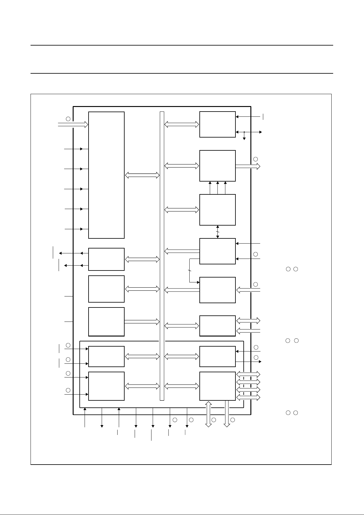
4 BLOCK DIAGRAM
handbook, full pagewidth
MBH348
33
1
1
4
2
0
3
3
RD
WR
AD0 to AD7
ADC0 to ADC7
A8 to A15
PSEN
XTAL2
XTAL1
EA
3 3 3 3
STADC
AV
SS
AV
DD
RST EWCMSR0 to CMSR5
CMT0, CMT1
RT2
T2
CT0I to CT3IP4P5RXDTXDP3P2P1P0
T0 T1 INT0 INT1
V
DD
V
SS
0
1
alternative function of port 0
alternative functions of port 1
2
3
alternative function of port 2
alternative function of port 3
4
5
alternative function of port 4
alternative function of port 5
THREE
16-BIT
COMPARA -
TORS
WITH
REGISTERS
PARALLEL
I/O PORTS
&
EXT. BUS
SERIAL
UART
PORT
8-BIT
I/O
PORTS
FOUR
16-BIT
CAPTURE
LATCHES
T2
16-BIT
TIMER/
EVENT
COUNTER
16
16
COMPARA -
TOR
OUTPUT
SELECTION
T3
WATCH -
DOG
TIMER
T0, T1
TWO 16-BIT
TIMER/
EVENT
COUNTERS
PCB
80C51
core
excluding
ROM/RAM
CPU
PROGRAM
MEMORY
DATA
MEMORY
DUAL
PWM
ADC
5
8 - bit
internal bus
8 KBYTES
ROM
PWM0
PWM1
256 BYTES
RAM
ALE
P8xC562
AV
REF+
AV
REF−
Fig.1 Block diagram.
1997 Apr 08 5
Philips Semiconductors Product specification
8-bit microcontroller P83C562; P80C562
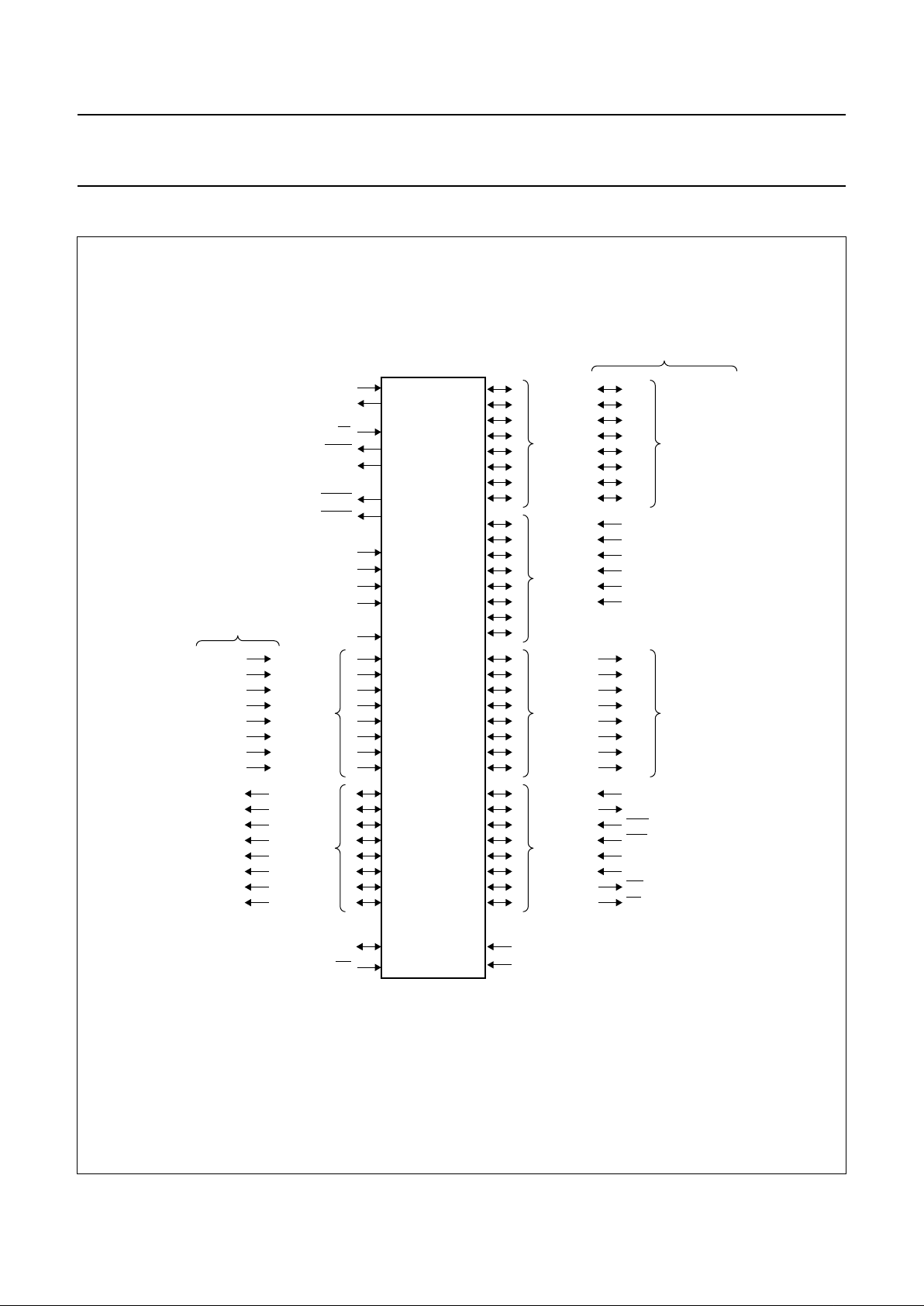
5 FUNCTIONAL DIAGRAM
Fig.2 Functional diagram.
handbook, full pagewidth
MBH347
0
1
2
3
4
5
6
7
PORT 0
SS
V
DD
V
0
1
2
3
4
5
6
7
PORT 1
0
1
2
3
4
5
6
7
PORT 3
AD0
AD1
AD2
AD3
AD4
AD5
AD6
AD7
LOW ORDER
ADDRESS
AND
DATA BUS
alternative function
0
1
2
3
4
5
6
7
PORT 2
A8
A9
A10
A11
A12
A13
A14
A15
HIGH ORDER
ADDRESS
BUS
CT0I
CT1I
CT2I
CT3I
T2
RT2
0
1
2
3
4
5
6
7
PORT 5
0
1
2
3
4
5
6
7
PORT 4
RST
EW
alternative function
ADC0
CMSR0
ADC1
ADC2
ADC3
ADC4
ADC5
ADC6
ADC7
CMSR1
CMSR2
CMSR3
CMSR4
CMSR5
CMT0
CMT1
AV
SS
AV
REF −
AV
REF +
STADC
DD
AV
PWM0
PWM1
XTAL1
XTAL2
RXD/DATA
TXD/CLOCK
T0
T1
RD
WR
INT1
INT0
P8xC562
PSEN
EA
ALE
1997 Apr 08 6
Philips Semiconductors Product specification
8-bit microcontroller P83C562; P80C562
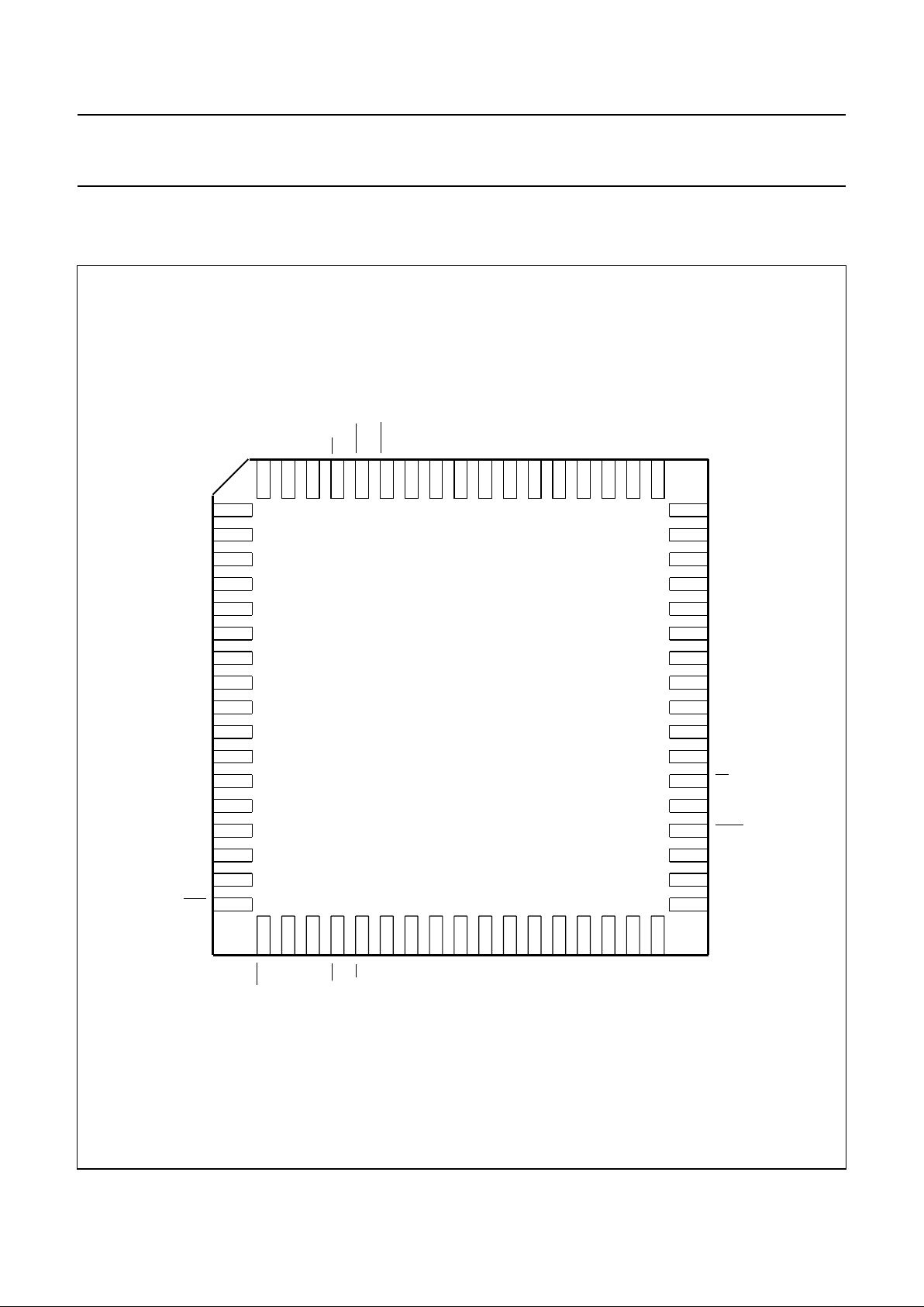
6 PINNING INFORMATION
6.1 Pinning
Fig.3 Pinning configuration for PLCC68 (SOT188-2) package.
handbook, full pagewidth
AV
SS
P0.0/AD0
P0.1/AD1
P0.2/AD2
P0.3/AD3
P0.4/AD4
P0.5/AD5
P0.6/AD6
P0.7/AD7
ALE
P2.7/A15
P2.6/A14
P2.5/A13
AV
REF+
AV
REF−
EA
PSEN
P5.4/ADC4
P5.0/ADC0
P5.1/ADC1
P5.2/ADC2
P5.3/ADC3
P5.5/ADC5
P5.6/ADC6
P4.0/CMSR0
STADC
V
DD
EW
PWM1
PWM0
P5.7/ADC7
AV
DD
P4.2/CMSR2
P4.1/CMSR1
P4.7/CMT1
P1.0/CT0I
P1.1/CT1I
P1.2/CT2I
P3.2/INT0
P4.3/CMSR3
P4.4/CMSR4
P4.5/CMSR5
P4.6/CMT0
RST
P1.3/CT3I
P1.4/T2
P1.5/RT2
P1.6
P1.7
P3.0/RXD
P3.1/TXD
P3.6/WR
P3.5/T1
P2.2/A10
n.c.
n.c.
n.c.
XTAL 2
XTAL 1
V
SS
P2.0/A8
P2.1/A9
V
SS
P3.7/RD
P2.4/A12
P2.3/A11
P3.4/T0
P3.3/INT1
27
28
29
30
31
32
33
34
35
36
37
38
39
40
41
42
43
9
8
7
6
5
4
3
2
1
68
67
66
65
64
63
62
61
10
11
12
13
14
15
16
17
18
19
20
21
22
23
24
25
26
60
59
58
57
56
55
54
53
52
51
50
49
48
47
46
45
44
MBH349
P8xC562

1997 Apr 08 7
Philips Semiconductors Product specification
8-bit microcontroller P83C562; P80C562
6.2 Pin description
Table 1 PLCC68 (SOT188-2)
To avoid latch-up at Power-on, the voltage at any pin at any time must lie within the range V
DD
+0.5VtoVSS− 0.5 V.
SYMBOL PIN DESCRIPTION
V
DD
2 Power supply, digital part (+5 V). Power supply pins during normal operation and
power reduction modes.
STADC 3 Start ADC operation: Input starting analog-to-digital conversion (ADC operation can
also be started by software). This pin must not float.
PWM0 4 Pulse Width Modulation output 0.
PWM1 5 Pulse Width Modulation output 1.
EW 6 Enable Watchdog Timer: enable for Watchdog Timer and disable Power-down mode.
This pin must not float.
P4.0/CMSR0
to
P4.5/CMSR5
7to12 P4.0 to P4.5: 8-bit quasi-bidirectional I/O port lines;
CMSR0 to CMSR5: Compare and Set/Reset outputs for Timer T2.
P4.6/CMT0 13 P4.6 to P4.7: 8-bit quasi-bidirectional I/O port lines;
CMT0 to CMT1: Compare and toggle outputs for Timer T2.
P4.7/CMT1 14
RST 15 Reset: Input to reset the P8x562; also generated when the Watchdog Timer overflows.
P1.0/CT0I
to
P1.3/CT3I
16 to 19 P1.0 to P1.3: 8-bit quasi-bidirectional I/O port lines;
CT0I to CT3I: Capture timer inputs for Timer 2.
P1.4/T2 20 P1.4: 8-bit quasi-bidirectional I/O port line;
T2: T2 event input (rising edge triggered).
P1.5/RT2 21 P1.5: 8-bit quasi-bidirectional I/O port line;
RT2: T2 timer reset input (rising edge triggered)
P1.6 to P1.7 22 to 23 P1.6 to P1.7: 8-bit quasi-bidirectional I/O port lines, open-drain.
P3.0/RXD 24 P3.0: 8-bit quasi-bidirectional I/O port line;
RXD: Serial input port.
P3.1/TXD 25 P3.1: 8-bit quasi-bidirectional I/O port line;
TXD: Serial output port.
P3.2/
INT0 26 P3.2: 8-bit quasi-bidirectional I/O port line;
INT0: External interrupt input 0.
P3.3/
INT1 27 P3.3: 8-bit quasi-bidirectional I/O port line;
INT1: External interrupt input 1.
P3.4/T0 28 P3.4: 8-bit quasi-bidirectional I/O port line;
T0: Timer 0 external input.
P3.5/T1 29 P3.5: 8-bit quasi-bidirectional I/O port line;
T1: Timer 1 external input.
P3.6/
WR 30 P3.6: 8-bit quasi-bidirectional I/O port line;
WR: External Data Memory Write strobe.
P3.7/
RD 31 P3.7: 8-bit quasi-bidirectional I/O port line;
RD: External Data Memory Read strobe.
n.c. 32, 33 Not connected.
XTAL2 34 Crystal Oscillator Output: output of the inverting amplifier that forms the oscillator.
Left open-circuit when an external oscillator clock is used.
1997 Apr 08 8
Philips Semiconductors Product specification
8-bit microcontroller P83C562; P80C562
XTAL1 35 Crystal Oscillator Input: input to the inverting amplifier that forms the oscillator, and
input to the internal clock generator. Receives the external oscillator clock signal when
an external oscillator is used.
V
SS
36, 37 Digital ground pins.
n.c. 38 Not connected.
P2.0/A08
to
P2.7/A15
39 to 46 P2.0 to P2.7: 8-bit quasi-bidirectional I/O port lines;
A08 to A15: High-order address byte for external memory.
PSEN 47 Program Store Enable: read strobe to the external program memory via Port 0 and 2.
Is activated twice each machine cycle during fetches from external program memory.
When executing out of external program memory two activations of PSEN are skipped
during each access to external data memory. PSEN is not activated (remains HIGH)
during no fetches from external program memory. PSEN can sink/source 8 LSTTL
inputs and can drive CMOS inputs without external pull-ups.
ALE 48 Address Latch Enable: latches the low byte of the address during access of external
memory in normal operation. It is activated every six oscillator periods except during an
external data memory access. ALE can sink/source 8 LSTTL inputs and can drive
CMOS inputs without an external pull-up. To prohibit the toggling of the ALE pin (RFI
noise reduction) the RFI bit in the Power Control Register must be set by software.
EA 49 External Access: if, during RESET, EA is HIGH the CPU executes out of the internal
program memory provided the program Counter is less than 8192. If, during RESET,
EA is LOW the CPU executes out of external program memory via Port 0 and Port 2.
EA is not allowed to float. EA is latched during RESET and don’t care after RESET.
P0.7/AD7
to
P0.0/AD0
50 to 57 P0.7 to P0.0: 8-bit open drain bidirectional I/O port lines;
AD7 to AD0: Multiplexed Low-order address and Data bus for external memory.
AV
REF-
58 Low-end of ADC (analog-to-digital conversion) reference resistor.
AV
REF+
59 High-end of ADC (analog-to-digital conversion) reference resistor.
AV
SS
60 Ground, analog part. For ADC receiver and reference voltage.
AV
DD
61 Power supply, analog part (+5 V). For ADC receiver and reference voltage.
P5.7/ADC7
to
P5.0/ADC0
62 to 68,1P5.7 to P5.0: 8-bit input port lines;
ADC7 to ADC0: eight analog ADC inputs
SYMBOL PIN DESCRIPTION

1997 Apr 08 9
Philips Semiconductors Product specification
8-bit microcontroller P83C562; P80C562
7 FUNCTIONAL DESCRIPTION
The P8xC562 is a stand-alone high-performance
microcontroller designed for use in real-time applications
such as instrumentation, industrial control and specific
automotive control applications.
In addition to the 80C51 standard functions, the device
provides a number of dedicated hardware functions for
these applications.
The P8xC562 is a control-oriented CPU with on-chip
program and data memory. It can be extended with
external program memory up to 64 kbytes. It can also
access up to 64 kbytes of external data memory.
For systems requiring extra capability, the P8xC562 can
be expanded using standard memories and peripherals.
The P8xC562 has two software selectable modes of
reduced activity for further power reduction − Idle and
Power-down. The Idle mode freezes the CPU while
allowing the RAM, timers, serial ports and interrupt system
to continue functioning. The Power-down mode saves the
RAM contents but freezes the oscillator causing all other
chip functions to be inoperative.
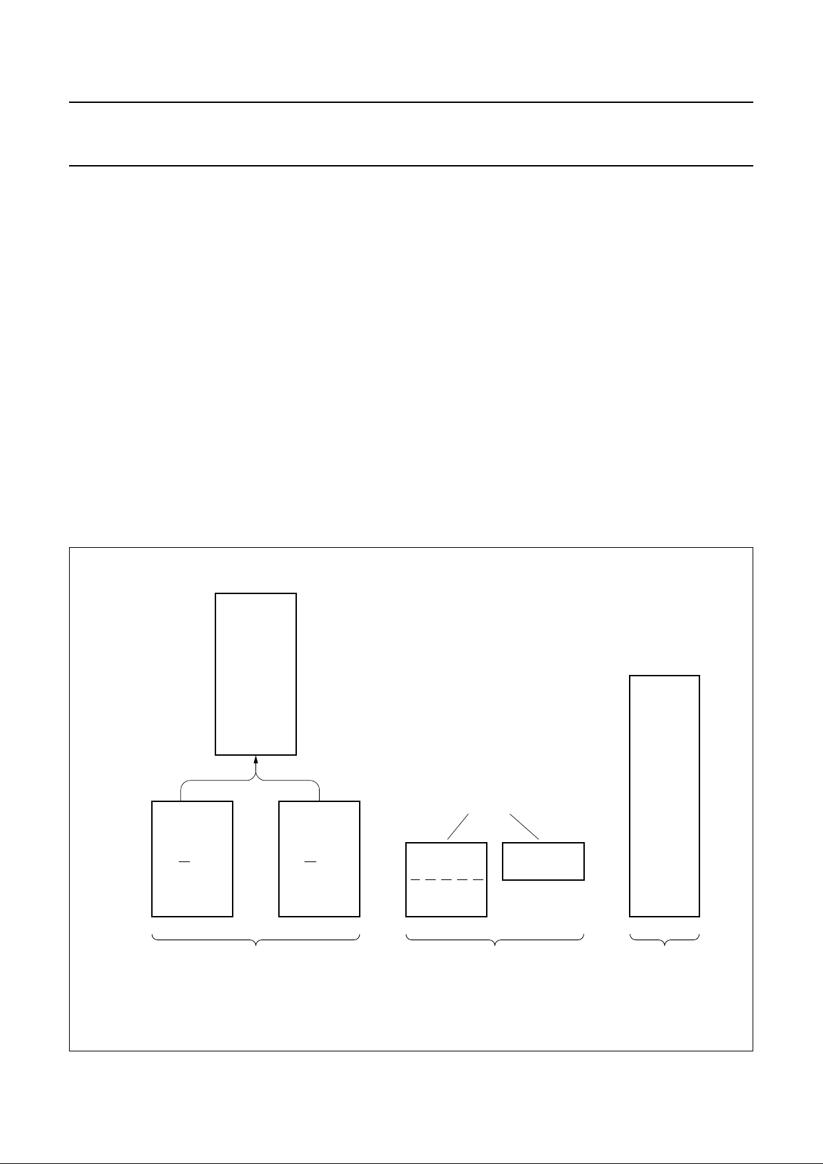
8 MEMORY ORGANIZATION
The Central Processing Unit (CPU) manipulates operands
in three memory spaces; these are the 64 kbyte external
data memory, 256 byte internal data memory and the
64 kbyte internal and external program memory.
The internal data memory is divided into 3 sections: the
lower 128 bytes of RAM, the upper 128 bytes of RAM and
the 128 byte Special Function Register memory
(see Fig.4). Figure 5 shows the Special Function
Registers memory map. Internal RAM locations 0 to 127
are directly and indirectly addressable. Internal RAM
locations 128 to 155 are only indirectly addressable.
The Special Function Register locations 128 to 255 are
only directly addressable.
The internal data RAM contains four register banks (each
with eight registers), 128 addressable bits, a scratch pad
area and the stack. The stack depth is limited by the
available internal data RAM and its location is determined
by the 8-bit Stack Pointer. All registers except the Program
Counter and the four 8-register banks reside in the
Special Function Register address space. These memory
mapped registers include arithmetic registers, pointers,
I/O ports, interrupt system registers, ADC and PWM
registers, timers and serial port registers. There are
120 addressable bit locations in the SFR address space.
The P8xC562 contains 256 bytes of internal data RAM
and 52 Special Function Registers. It provides a
non-paged program memory address space to
accommodate relocatable code. Conditional branches are
performed relative to the Program Counter.
The register-indirect jump permits branching relative to a
16-bit base register with an offset provided by an 8-bit
index register. 16-bit jumps and calls permit branching to
any location in the contiguous 64 kbyte program memory
address space.
8.1 Program Memory
The program memory address space of the P83C562
consists of internal and external memory. The P83C562
has 8 kbytes of program memory on-chip. The program
memory can be externally expanded up to 64 kbytes. If the
EA pin is held HIGH, the P83C562 executes out of the
internal program memory unless the address exceeds
1FFFH then locations 2000H through to 0FFFFH are
fetched from the external program memory. If theEA pin is
held LOW, the P83C562 fetches all instructions from the
external memory. Figure 4 illustrates the program
memory address space.
By setting a mask programmable security bit (i.e. user
dependent) the ROM content is protected i.e. it cannot be
read at any time by any test mode or by any instruction in
the external program memory space. The MOVC
instructions are the only ones which have access to
program code in the internal or external program memory.
TheEA input is latched during reset and is ‘don’t care’ after
reset. This implementation prevents from reading internal
program code by switching from the external program
memory to internal program memory during MOVC
instruction or an instruction that handles immediate data.
Table 2 lists the access to internal and external program
memory by the MOVC instructions when the security bit
has been set to a logic 1. If the security bit has been set to
a logic 0 there are no restrictions for the MOVC
instructions.
Table 2 Memory access by the MOVC instruction
MOVC
INSTRUCTION
PROGRAM MEMORY ACCESS
INTERNAL EXTERNAL
MOVC in internal
program memory
YES YES
MOVC in external
program memory
NO YES
1997 Apr 08 10
Philips Semiconductors Product specification
8-bit microcontroller P83C562; P80C562
8.2 Addressing
The P8xC562 has five methods for addressing source
operands:
• Register
• Direct
• Register-Indirect
• Immediate
• Base-Register plus Index-Register-Indirect.
The first three methods can be used for addressing
destination operands. Most instructions have a
'destination/source' field that specifies the data type,
addressing methods and operands involved.
For operations other than MOVs, the destination operand
is also a source operand.
Access to memory addressing is as follows:
• Registers in one of the four 8-register banks through
Register, Direct or Register-Indirect
• 256 bytes of internal data RAM through Direct or
Register-Indirect. Bytes 0 to 127 may be addressed
directly/indirectly. Bytes 128 to 155 share their address
locations with the SFR registers and so may only be
addressed indirectly as data RAM
• Special Function Registers through Direct at address
locations 128 to 255
• External data memory through Register-Indirect
• Program memory look-up tables through Base-Register
plus Index-Register-Indirect.
The P8xC562 is classified as an 8-bit device since the
internal ROM, RAM, Special Function Registers,
Arithmetic Logic Unit and external data bus are all 8-bits
wide. It performs operations on bit, nibble, byte and
double-byte data types.
Facilities are available for byte transfer, logic and integer
arithmetic operations. Data transfer, logic and conditional
branch operations can be performed directly on Boolean
variables to provide excellent bit handling.
Fig.4 Memory map.
handbook, full pagewidth
MBC745
INDIRECT ONLY
DIRECT AND
INDIRECT
255
127
0
EXTERNAL
(EA = 0)
INTERNAL
(EA = 1)
INTERNAL DATA MEMORY
EXTERNAL
DATA MEMORY
PROGRAM MEMORY
EXTERNAL
64K
64K
8192
8191
0
OVERLAPPED SPACE
0
8191
0
SPECIAL
FUNCTION
REGISTERS

1997 Apr 08 11
Philips Semiconductors Product specification
8-bit microcontroller P83C562; P80C562
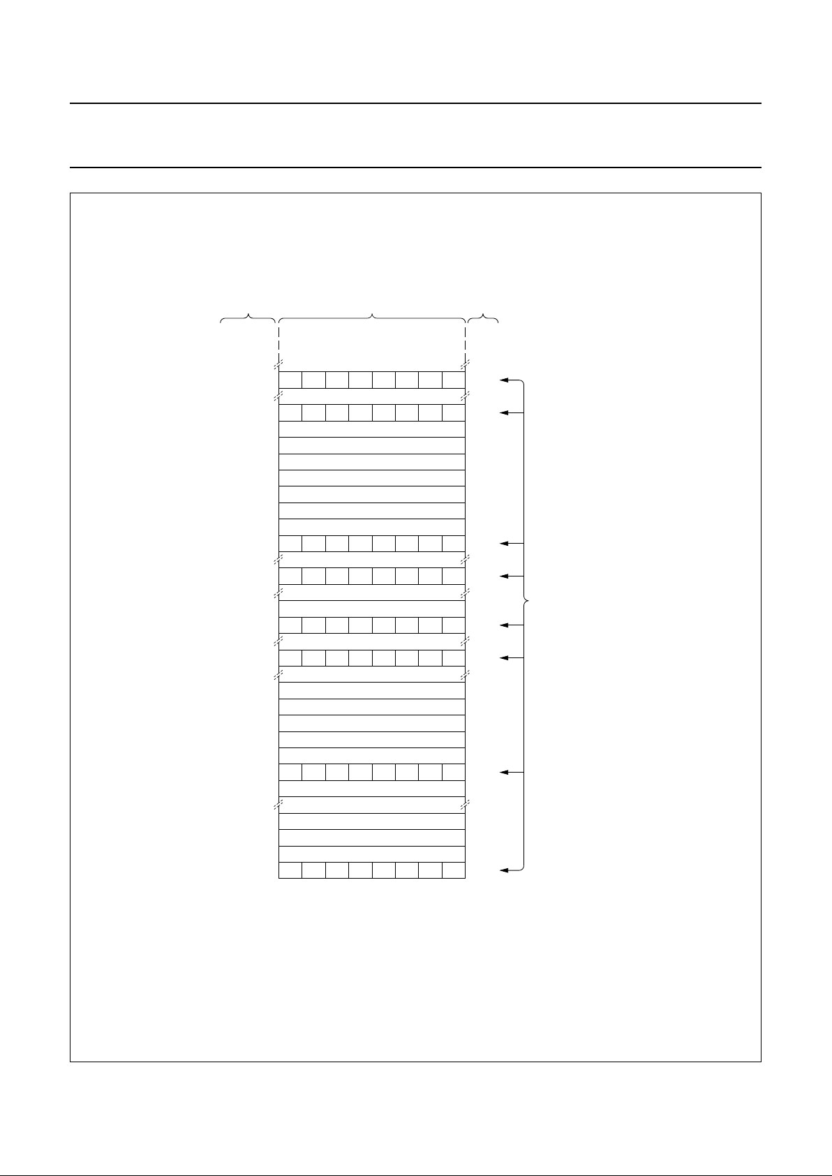
Fig.5 Special Function Register memory map.
handbook, full pagewidth
MBH346
FEFF FD FC FB FA F9 F8
F6F7 F5 F4 F3 F2 F1 F0
EEEF ED EC EB EA E9 E8
E6E7 E5 E4 E3 E2 E1 E0
D6D7 D5 D4 D3 D2 D1 D0
CECF CD CC CB CA C9 C8
C6C7 C5 C4 C3 C2 C1 C0
BIT ADDRESS
REGISTER
MNEMONIC
FFH
DIRECT
BYTE
ADDRESS (HEX)
FEH
FDH
FCH
F8H
F0H
EFH
EEH
EDH
ECH
EBH
EAH
E8H
E0H
DBH
DAH
D9H
D8H
D0H
CFH
CEH
CDH
CCH
CBH
CAH
C9H
C8H
C6H
C5H
C4H
C0H
SFRs containing
directly addressable
bits
Reserved for I
2
C-bus
T3
PWMP
PWM1
PWM0
IP1
B
RTE
STE
# TMH2
# TML2
CTCON
TM2CON
IEN1
ACC
PSW
# CTH3
# CTH2
# CTH1
# CTH0
CMH2
CMH1
CMH0
TM2IR
# ADCH
ADCON
# P5
P4
# denotes read-only registers
1997 Apr 08 12
Philips Semiconductors Product specification
8-bit microcontroller P83C562; P80C562
handbook, full pagewidth
MGA151
BEBF BD BC BB BA B9 B8
B6B7 B5 B4 B3 B2 B1 B0
AEAF AD AC AB AA A9 A8
A6A7 A5 A4 A3 A2 A1 A0
9E9F 9D 9C 9B 9A 99 98
9697 95 94 93 92 91 90
8E8F 8D 8C 8B 8A 89 88
8687 85 84 83 82 81 80
BIT ADDRESS
REGISTER
MNEMONIC
DIRECT
BYTE
ADDRESS (HEX)
B8H
B0H
AFH
AEH
ADH
ACH
ABH
AAH
A8H
A0H
99H
98H
90H
8DH
8CH
8BH
8AH
89H
88H
87H
83H
82H
81H
80H
SFRs containing
directly addressable
bits
IP0
P3
# CTL3
P2
S0BUF
S0CON
P1
TH1
TH0
TL1
TL0
TMOD
PCON
DPH
DPL
SP
P0
# denotes read-only registers
# CTL2
# CTL1
# CTL0
CML2
CML1
CML0
IEN0
TCON
A9H
Fig.6 Special Function Register memory map (continued).
1997 Apr 08 13
Philips Semiconductors Product specification
8-bit microcontroller P83C562; P80C562
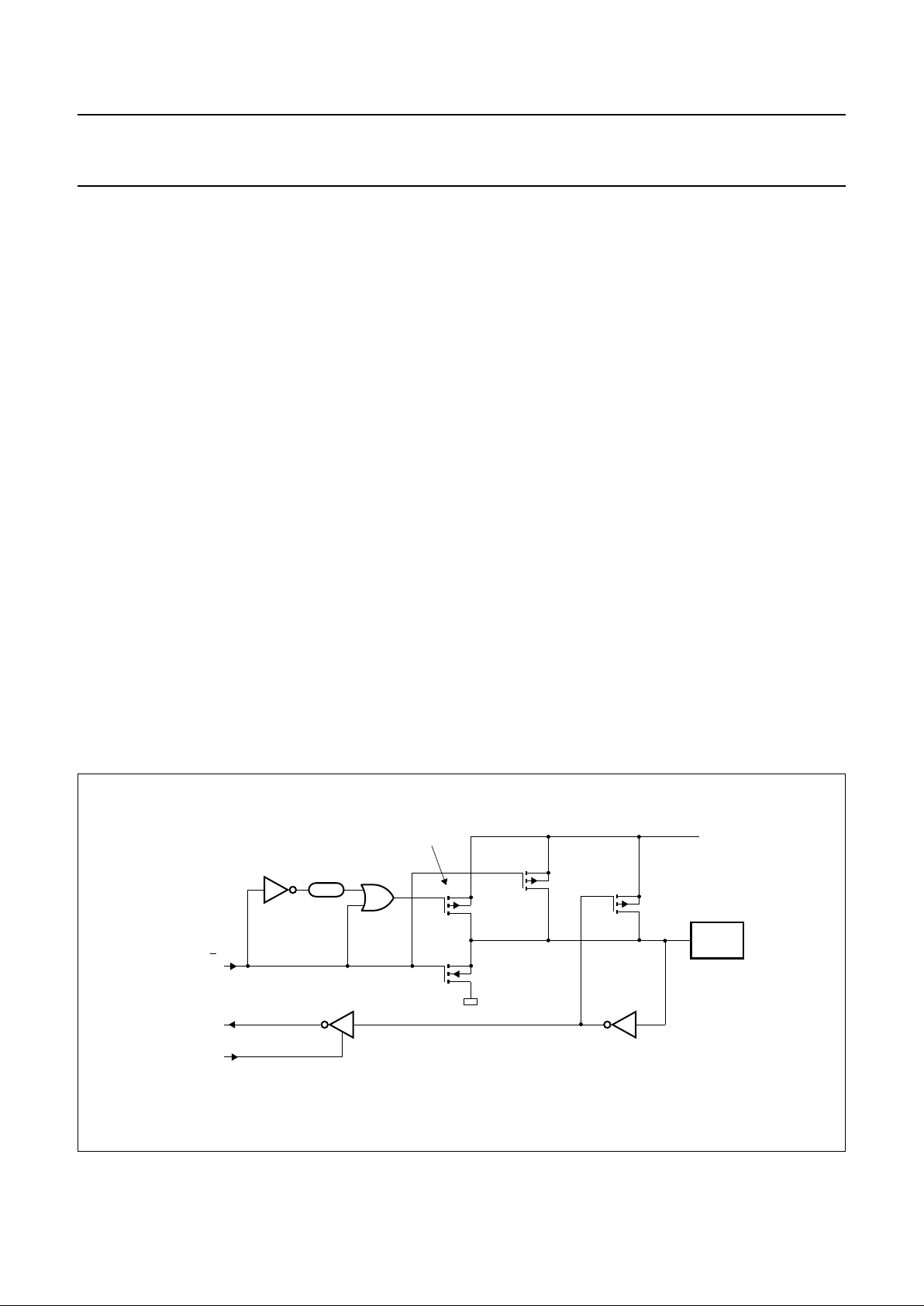
9 I/O FACILITIES
The P8xC562 has six 8-bit ports. Ports 0 to 3 are the same
as in the 80C51, with the exception of the additional
functions of Port 1. The parallel I/O function of Port 4 is
equal to that of Ports 1, 2 and 3. Port 5 has a parallel input
port function, but has no function as an output port.
Ports 0 to 5 perform the following alternative functions:
Port 0 Provides the multiplexed low-order address and
data bus used for expanding the P8xC562 with
standard memories and peripherals.
Port 1 is used for a number of special functions:
• 4 capture inputs (or external interrupt request inputs if
capture information is not utilized)
• External counter input
• External counter reset input.
Port 2 Provides the high-order address bus when
expanding the P8xC562 with external program
memory and/or external data memory.
Port 3 Pins can be configured individually to provide:
• External interrupt request inputs
• Counter inputs
• Serial port receiver input and transmitter output
• Control signals to READ and WRITE external data
memory.
Port 4 Can be configured to provide signals indicating a
match between timer counter T2 and its compare
registers.
Port 5 May be used in conjunction with the ADC interface.
Unused analog inputs can be used as digital inputs.
As Port 5 lines may be used as inputs to the ADC,
these digital inputs have an inherent hysteresis to
prevent the input logic from drawing too much
current from the power lines when driven by analog
signals. Channel-to-channel crosstalk should be
taken into consideration when both digital and
analog signals are simultaneously input to Port 5
(see Chapter 20).
All ports are bidirectional with the exception of Port 5 which
is an input port. Alternative function bits which are not used
may be used as normal bidirectional I/O pins.
The generation or use of a Port 1, Port 3 or Port 4 pin as
an alternative function is carried out automatically by the
P8xC562 provided the associated Special Function
Register bit is set HIGH.
In addition to the standard 8-bit ports, the I/O facilities of
the P8xC562 also include a number of special I/O lines.
Fig.7 I/O buffers in the P8xC562 (Ports 2, 3, 4 and P1.0 to P1.5).
handbook, full pagewidth
MLA513
p1
p2
p3
input data
read port pin
2 oscillator
periods
n
strong pull-up
I/O PIN
PORT
+5 V
I1
Q
from port latch
INPUT
BUFFER
1997 Apr 08 14
Philips Semiconductors Product specification
8-bit microcontroller P83C562; P80C562
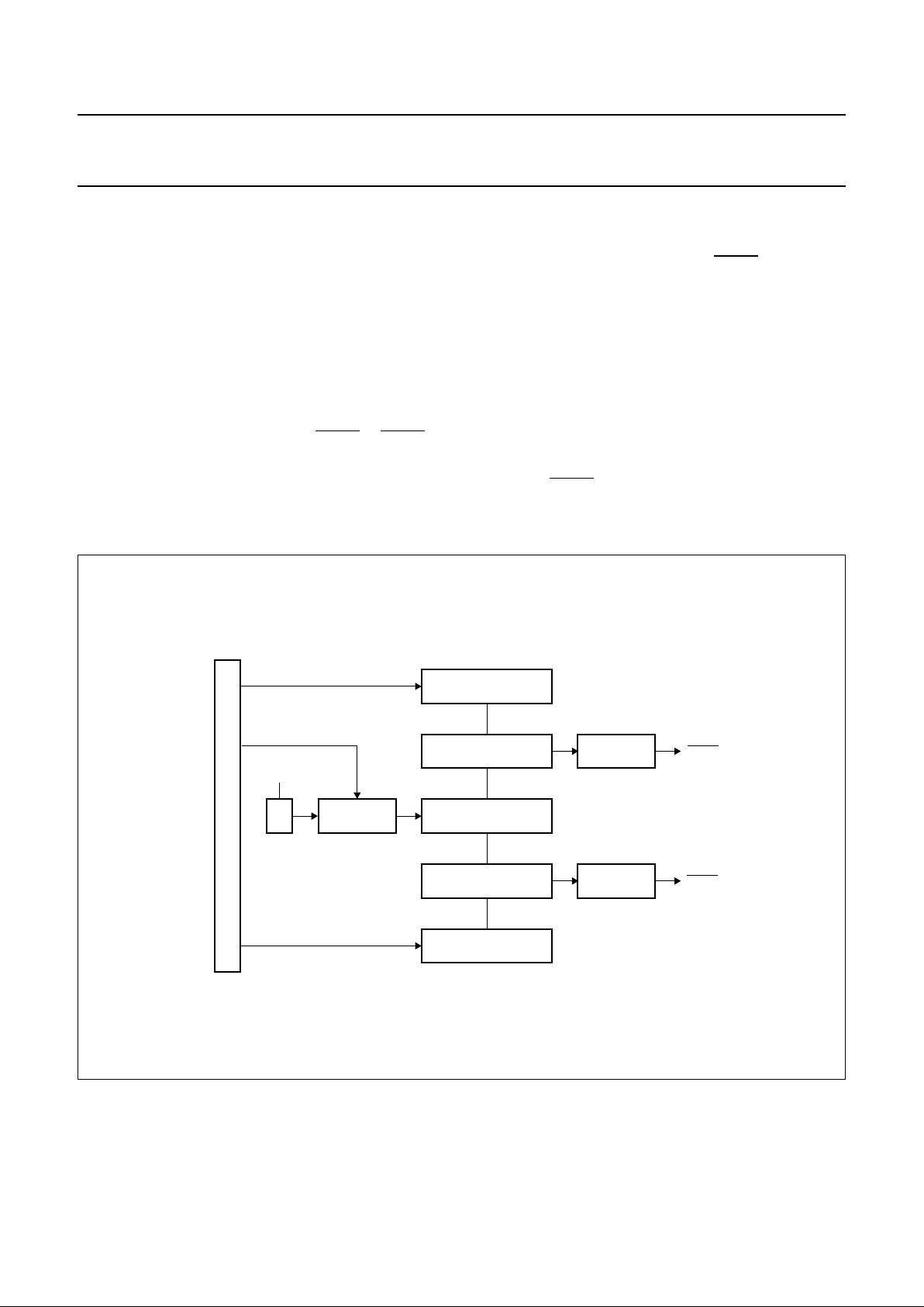
10 PULSE WIDTH MODULATED OUTPUTS
Two pulse width modulated output channels are provided
with the P8xC562. These channels output pulses of
programmable length and interval. The repetition
frequency is defined by an 8-bit prescaler PWMP which
generates the clock for the counter. Both the prescaler and
counter are common to both PWM channels. The 8-bit
counter counts modulo 255 i.e. from 0 to 254 inclusive.
The value of the 8-bit counter is compared to the contents
of two registers: PWM0 and PWM1.
Provided the contents of either of these registers is greater
than the counter value, the output of PWM0 or PWM1 is
set LOW. If the contents of these registers are equal to, or
less than the counter value, the output will be HIGH.
The pulse width ratio is therefore defined by the contents
of the registers PWM0 and PWM1.
The pulse width ratio is in the range of 0 to 255/255 and
may be programmed in increments of 1/255.
The repetition frequency f
PWM
, at the PWMn outputs is
given by:
When using an oscillator frequency of 16 MHz for
example, the above formula would give a repetition
frequency range of 123 Hz to 31.4 kHz.
By loading the PWM registers with either 00H or FFH, the
PWM outputs can be retained at a constant HIGH or LOW
level respectively. When loading FFH to the PWM
registers, the 8-bit counter will never actually reach this
value. Both
PWMn output pins are driven by push-pull
drivers, and are not shared with any other function.
f
PWM
f
OSC
2 1 PWMP+()× 255×
------------------------------------------------------------ -
=
Fig.8 Functional diagram of Pulse Width Modulated outputs.
handbook, full pagewidth
MBC746
I
N
T
E
R
N
A
L
B
U
S
f
osc
PWMP
PWM1
PRESCALER
8-BIT COUNTER
1/2
PMW0
8-BIT COMPARATOR
8-BIT
COMPARATOR
OUTPUT
BUFFER
PWM1
OUTPUT
BUFFER
PWM0
1997 Apr 08 15
Philips Semiconductors Product specification
8-bit microcontroller P83C562; P80C562
10.1 Prescaler Frequency Control Register (PWMP)
Table 3 Prescaler Frequency Control Register (SFR address FEH)
Table 4 Description of PWMP bits
10.2 Pulse Width Register 0 (PWM0)
Table 5 Pulse Width Register 0 (SFR address FCH)
Table 6 Description of PWM0 bits
10.3 Pulse Width Register 1 (PWM1)
Table 7 Pulse Width Register 1 (SFR address FDH)
Table 8 Description of PWM1 bits
76543210
PWMP.7 PWMP.6 PWMP.5 PWMP.4 PWMP.3 PWMP.2 PWMP.1 PWMP.0
BIT SYMBOL DESCRIPTION
7
to
0
PWMP.7
to
PWMP.0
Prescaler division factor.
The prescaler division factor = (PWMP) + 1.
76543210
PWM0.7 PWM0.6 PWM0.5 PWM0.4 PWM0.3 PWM0.2 PWM0.1 PWM0.0
BIT SYMBOL DESCRIPTION
7
to
0
PWM0.7
to
PWM0.0
Pulse width ratio.
76543210
PWM1.7 PWM1.6 PWM1.5 PWM1.4 PWM1.3 PWM1.2 PWM1.1 PWM1.0
BIT SYMBOL DESCRIPTION
7
to
0
PWM1.7
to
PWM1.0
Pulse width ratio.
LOW/HIGH ratio of PWMn signals
PWMn()
255 PWMn()–
----------------------------------------- -
=
LOW/HIGH ratio of PWMn signals
PWMn()
255 PWMn()–
----------------------------------------- -
=
1997 Apr 08 16
Philips Semiconductors Product specification
8-bit microcontroller P83C562; P80C562
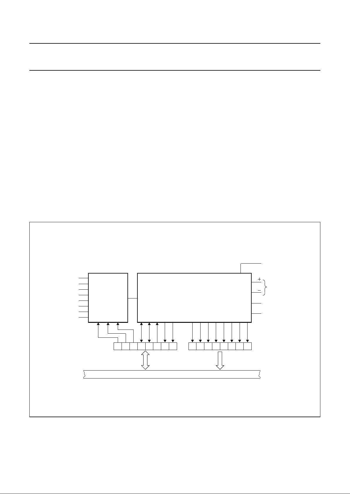
11 ANALOG-TO-DIGITAL CONVERTER (ADC)
The completion of the 8-bit ADC conversion is flagged by
ADCI in the ADCON register and the result is stored in
Special Function Register ADCH.
An ADC conversion in progress is unaffected by an
external or software ADC start. The result of a completed
conversion remains unaffected provided ADCI = 1. While
ADCS = 1 or ADCI = 1, a new ADC start will be blocked
and consequently lost.
An ADC conversion already in progress is aborted when
the Idle or Power-down mode is entered. The result of a
completed conversion (ADCI = 1) remains unaffected
when entering the Idle mode.
If ADCI is cleared by software and ADCS is set at the same
time, a new analog-to-digital conversion with the same
channel number, may be started. However, it is
recommended to reset ADCI before ADCS is set.
11.1 Analog input pins
The analog input circuitry consists of an 8-input analog
multiplexer and an ADC with 8-bit resolution. The analog
reference voltage and analog power supplies are
connected via separate input pins. The conversion takes
24 machine cycles i.e. 18 µs at an oscillator frequency of
16 MHz.
The ADC is controlled using the ADC Control Register
(ADCON). Input channels are selected by the analog
multiplexer, using bits AADR.0 to AADR.2 in ADCON.
Fig.9 Functional diagram of analog input.
handbook, full pagewidth
MBH350
ADC0
ANALOG INPUT
MULTIPLEXER
8-BIT ADC
ADCON
1234567012345670
STADC
analog reference
supply (analog part)
ground (analog part)
ADCH
INTERNAL BUS
ADC1
ADC2
ADC3
ADC4
ADC5
ADC6
ADC7
 Loading...