

Philips P80C552EBA-08, P80C552EHB-08, P80C552IBB-08, P80C552ABA-08, P80C552IFB-08 Datasheet
...
80C552/83C552
Single-chip 8-bit microcontroller
Product specification
Supersedes data of 1998 Jan 06
IC20 Data Handbook
1998 Aug 13
INTEGRATED CIRCUITS

Philips Semiconductors Product specification
80C552/83C552
Single-chip 8-bit microcontroller
Single-chip 8-bit microcontroller with 10-bit A/D, capture/compare timer, high-speed outputs, PWM
2
1998 Aug 13
DESCRIPTION
The 80C552/83C552 (hereafter generically
referred to as 8XC552) Single-Chip 8-Bit
Microcontroller is manufactured in an
advanced CMOS process and is a derivative
of the 80C51 microcontroller family. The
8XC552 has the same instruction set as the
80C51. Three versions of the derivative exist:
• 83C552—8k bytes mask programmable
ROM
• 80C552—ROMless version of the 83C552
• 87C552—8k bytes EPROM (described in a
separate chapter)
The 8XC552 contains a non-volatile 8k × 8
read-only program memory (83C552), a
volatile 256 × 8 read/write data memory, five
8-bit I/O ports, one 8-bit input port, two 16-bit
timer/event counters (identical to the timers of
the 80C51), an additional 16-bit timer coupled
to capture and compare latches, a 15-source,
two-priority-level, nested interrupt structure,
an 8-input ADC, a dual DAC pulse width
modulated interface, two serial interfaces
(UART and I
2
C-bus), a “watchdog” timer and
on-chip oscillator and timing circuits. For
systems that require extra capability, the
8XC552 can be expanded using standard
TTL compatible memories and logic.
In addition, the 8XC552 has two software
selectable modes of power reduction—idle
mode and power-down mode. The idle mode
freezes the CPU while allowing the RAM,
timers, serial ports, and interrupt system to
continue functioning. The power-down mode
saves the RAM contents but freezes the
oscillator, causing all other chip functions to
be inoperative.
The device also functions as an arithmetic
processor having facilities for both binary and
BCD arithmetic plus bit-handling capabilities.
The instruction set consists of over 100
instructions: 49 one-byte, 45 two-byte, and
17 three-byte. With a 16MHz (24MHz)
crystal, 58% of the instructions are executed
in 0.75µs (0.5µs) and 40% in 1.5µs (1µs).
Multiply and divide instructions require 3µs
(2µs).
FEATURES
• 80C51 central processing unit
• 8k × 8 ROM expandable externally to 64k
bytes
• ROM code protection
• An additional 16-bit timer/counter coupled
to four capture registers and three compare
registers
• Two standard 16-bit timer/counters
• 256 × 8 RAM, expandable externally to 64k
bytes
• Capable of producing eight synchronized,
timed outputs
• A 10-bit ADC with eight multiplexed analog
inputs
• Two 8-bit resolution, pulse width
modulation outputs
• Five 8-bit I/O ports plus one 8-bit input port
shared with analog inputs
LOGIC SYMBOL
• I
2
C-bus serial I/O port with byte oriented
master and slave functions
• Full-duplex UART compatible with the
standard 80C51
• On-chip watchdog timer
• Three speed ranges:
– 3.5 to 16MHz
– 3.5 to 24MHz (ROM, ROMless only)
– 3.5 to 30MHz (ROM, ROMless only)
• Three operating ambient temperature
ranges:
– P83C552xBx: 0°C to +70°C
– P83C552xFx: –40°C to +85°C
(XTAL frequency max. 24 MHz)
– P83C552xHx: –40°C to +125°C
(XTAL frequency max. 16 MHz)
PORT 5
PORT 4
ADC0-7
CMT0
CMT1
CMSR0-5
RST
EW
XTAL1
XTAL2
EA
ALE
PSEN
AVref+
AVref–
STADC
PWM0
PWM1
PORT 0
LOW ORDER
ADDRESS AND
DATA BUS
PORT 1PORT 2PORT 3
CT0I
CT1I
CT2I
CT3I
T2
RT2
SCL
SDA
RxD/DATA
TxD/CLOCK
INT0
INT1
T0
T1
WR
RD
V
SS
V
DD
AV
SS
AV
DD
HIGH ORDER
ADDRESS AND
DATA BUS
Philips Semiconductors Product specification
80C552/83C552
Single-chip 8-bit microcontroller
1998 Aug 13
3
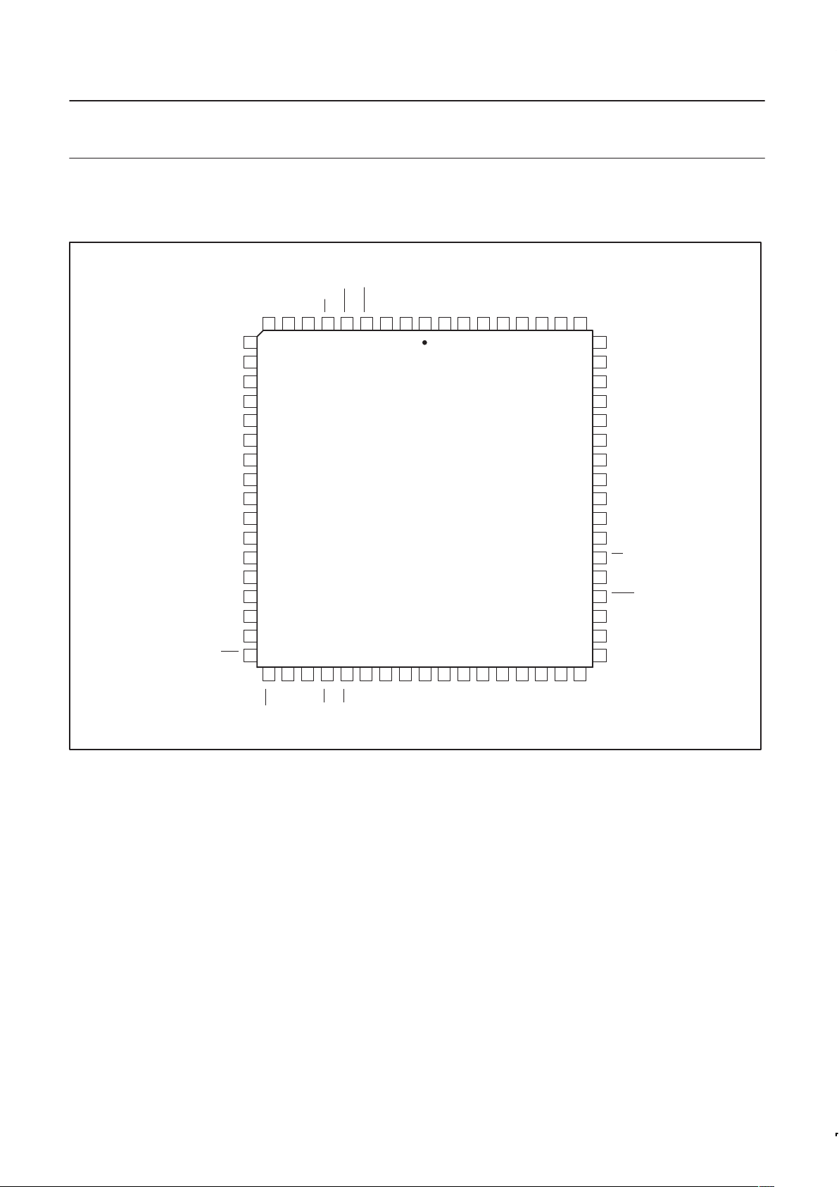
PIN CONFIGURATIONS
Plastic Leaded Chip Carrier
NC*
P3.7/RD
P3.6/WR
P5.0/ADC0
10
11
12
13
14
15
16
30 31 32 33 34 35 36
P4.3/CMSR3
P4.4/CMSR4
P4.5/CMSR5
P4.6/CMT0
P4.7/CMT1
P1.0/CT0I
RST
37 3828 29
17
18
19
20
P1.1/CT1I
P1.2/CT2I
P1.4/T2
P1.3/CT3I
PLASTIC LEADED CHIP CARRIER
SU00932
21
22
23
24
25
26
P1.5/RT2
P1.6/SCL
P1.7/SDA
P3.0/RxD
P3.2/INT0
P3.1/TxD
39 40 41 42 43
P3.4/T0
P3.5/T1
NC*
NC*
XTAL2
XTAL1
V
SS
P2.1/A09
P2.2/A10
P2.3/A11
P2.4/A12
60
59
58
57
56
55
54
AV
SS
AV
REF+
AV
REF–
P0.0/AD0
P0.1/AD1
P0.3/AD3
P0.2/AD2
53
52
51
50
P0.4/AD4
P0.5/AD5
P0.7/AD7
P0.6/AD6
49
48
47
46
45
44
EA
ALE
PSEN
P2.7/A15
P2.5/A13
P2.6/A14
44
765432168 6798 66 65 64 63 62
P4.2/CMSR2
P4.1/CMSR1
P4.0/CMSR0
EW
PWM1
PWM0
STADC
P5.1/ADC1
P5.2/ADC2
P5.3/ADC3
P5.4/ADC4
P5.5/ADC5
P5.6/ADC6
P5.7/ADC7
61
27
AV
DD
V
DD
P3.3/INT1
V
SS
P2.0/A08
* Do not connect.
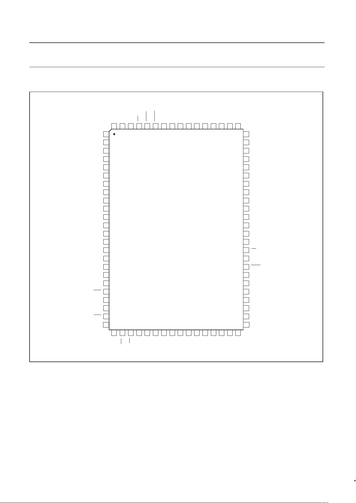
Philips Semiconductors Product specification
80C552/83C552
Single-chip 8-bit microcontroller
1998 Aug 13
4
Plastic Quad Flat Pack
V
DD
1
2
3
4
5
6
7
27 28 29 30 31 32 33
P4.1/CMSR1
P4.2/CMSR2
NC*
P4.3/CMSR3
P4.4/CMSR4
P4.6/CMT0
P4.5/CMSR5
34 3525 26
8
9
10
11
P4.7/CMT1
RST
P1.1/CT1I
P1.0/CT0I
PLASTIC QUAD FLAT PACK
SU00931
12
13
14
15
16
17
P1.2/CT2I
P1.3/CT3I
P1.4/T2
P1.5/RT2
P1.7/SDA
P1.6/SCL
18
19
20
21
P3.0/RxD
P3.1/TxD
NC*
P3.2/INT0
22
23
24
NC*
P3.3/INT1
PP3.4/T0
36 37 38 39 40
P3.5/T1
P3.6/WR
P3.7/RD
NC*
NC*
NC*
XTAL2
XTAL1
IC
V
SSVSSVSS
NC*
P2.0/A08
P2.1/A09
P2.2/A10
64
63
62
61
60
59
58
P5.7/ADC7
AV
DD
NC*
AV
SS
AV
REF+
P0.0/AD0
AV
REF–
57
56
55
54
P0.1/AD1
P0.2/AD2
P0.4/AD4
P0.3/AD3
53
52
51
50
49
48
P0.5/AD5
P0.6/AD6
P0.7/AD7
EA
PSEN
ALE
47
46
45
44
P2.7/A15
P2.6/A14
NC*
P2.5/A13
43
42
41
NC*
P2.4/A12
P2.3/A11
78 77 76 75 74 73 72 71 7080 79 69 68 67 66 65
P4.0/SMSR0
NC*
NC*
EW
PWM1
PWM0
STADC
IC
P5.0/ADC0
P5.1/ADC1
P5.2/ADC2
P5.3/ADC3
P5.4/ADC4
P5.5/ADC5
P5.6/ADC6
* Do not connect.
IC = Internally connected (do not use).
Philips Semiconductors Product specification
80C552/83C552
Single-chip 8-bit microcontroller
1998 Aug 13
5
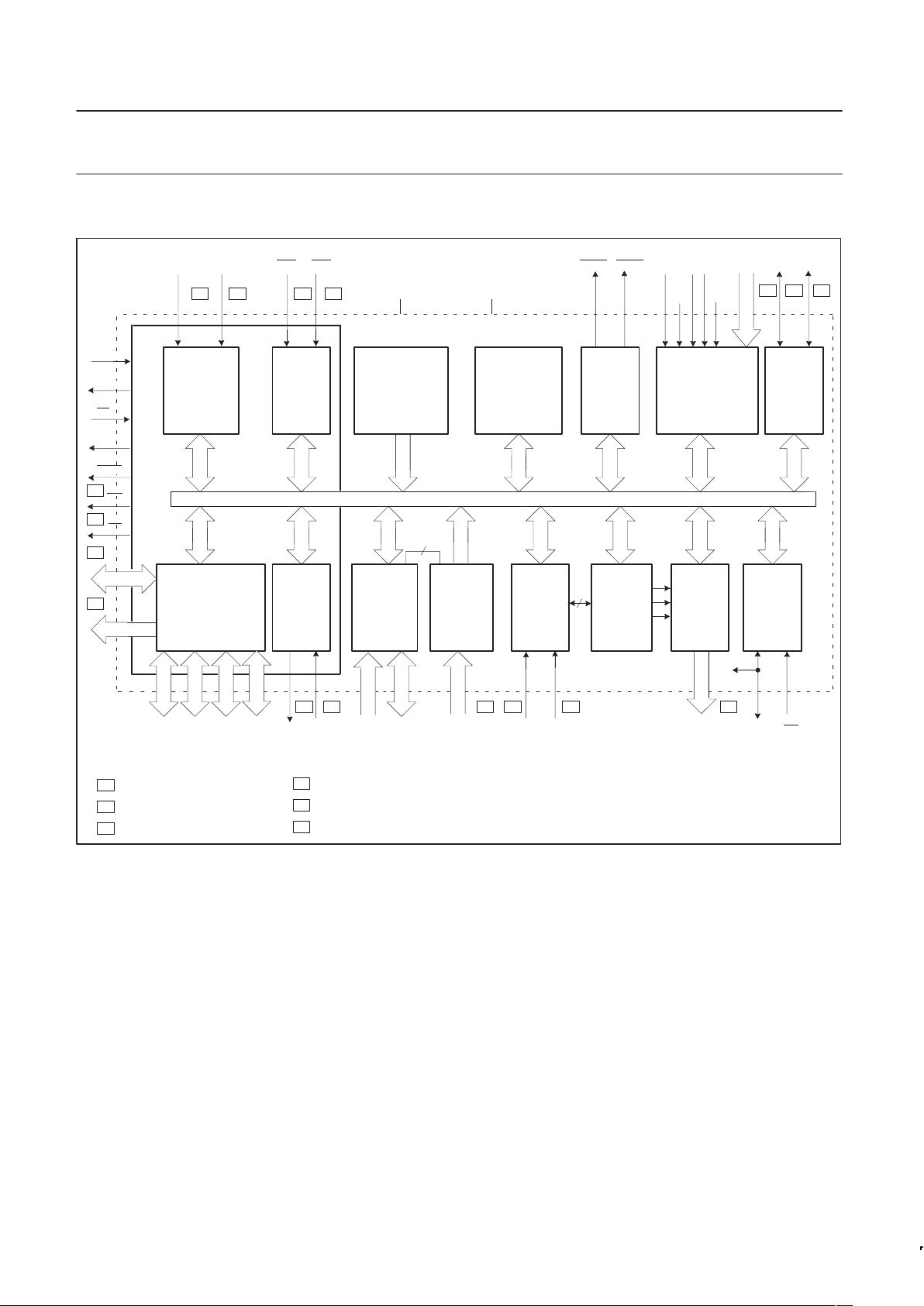
BLOCK DIAGRAM
CPU
ADC
8-BIT INTERNAL BUS
16
P0 P1 P2 P3 TxD RxD P5 P4 CT0I-CT3I T2 RT2 CMSR0-CMSR5
CMT0, CMT1
RST EW
XTAL1
XTAL2
EA
ALE
PSEN
WR
RD
T0 T1 INT0 INT1
V
DD
V
SS
PWM0 PWM1
AV
SS
AV
DD
AV
REF
–+
STADC
ADC0-7 SDA SCL
3 3 3 3
3 3
0
2
1 1 1 4
115
0
1
2
ALTERNATE FUNCTION OF PORT 0
3
4
5
AD0-7
A8-15
3
3
16
T0, T1
TWO 16-BIT
TIMER/EVENT
COUNTERS
PROGRAM
MEMORY
8k x 8 ROM
DATA
MEMORY
256 x 8 RAM
DUAL
PWM
SERIAL
I
2
C PORT
80C51 CORE
EXCLUDING
ROM/RAM
PARALLEL I/O
PORTS AND
EXTERNAL BUS
SERIAL
UART
PORT
8-BIT
PORT
FOUR
16-BIT
CAPTURE
LATCHES
T2
16-BIT
TIMER/
EVENT
COUNTERS
T2
16-BIT
COMPARA-
TORS
wITH
REGISTERS
COMPARA-
TOR
OUTPUT
SELECTION
T3
WATCHDOG
TIMER
ALTERNATE FUNCTION OF PORT 1
ALTERNATE FUNCTION OF PORT 2
ALTERNATE FUNCTION OF PORT 3
ALTERNATE FUNCTION OF PORT 4
ALTERNATE FUNCTION OF PORT 5
Philips Semiconductors Product specification
80C552/83C552
Single-chip 8-bit microcontroller
1998 Aug 13
6
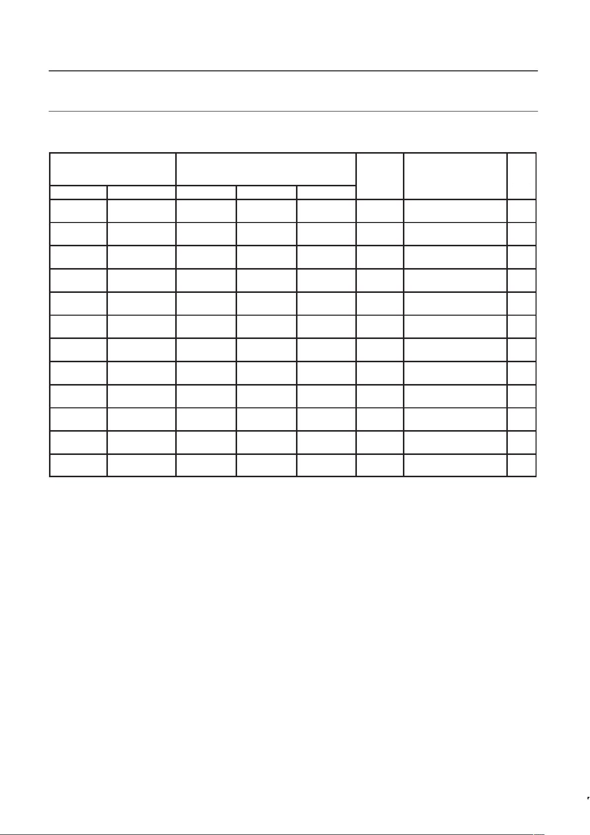
ORDERING INFORMATION
PHILIPS
PART ORDER NUMBER
PART MARKING
NORTH AMERICA PHILIPS
PART ORDER NUMBER
DRAWING
NUMBER
TEMPERATURE (°C)
AND PACKAGE
FREQ
(MHz)
ROMless ROM
1
ROMless ROM EPROM
2
()
P80C552EBA P83C552EBA/xxx S80C552-4A68 S83C552-4A68 S87C552-4A68 SOT188-2
0 to +70,
Plastic Leaded Chip Carrier
16
P80C552EBB P83C552EBB/xxx S80C552-4B S83C552-4B S87C552-4BA SOT318-2
0 to +70,
Plastic Quad Flat Pack
16
P80C552EFA P83C552EFA/xxx S80C552-5A68 S83C552-5A68 S87C552-5A68 SOT188-2
–40 to +85,
Plastic Leaded Chip Carrier
16
P80C552EFB P83C552EFB/xxx S80C552-5B S83C552-5B SOT318-2
–40 to +85,
Plastic Quad Flat Pack
16
P80C552EHA P83C552EHA/xxx S80C552-6A68 S83C552-6A68 SOT188-2
–40 to +125,
Plastic Leaded Chip Carrier
16
P80C552EHB P83C552EHB/xxx S80C552-6B S83C552-6B SOT318-2
–40 to +125,
Plastic Quad Flat Pack
16
P80C552IBA P83C552IBA/xxx S80C552-AA68 S83C552-AA68 SOT188-2
0 to +70,
Plastic Leaded Chip Carrier
24
P80C552IBB P83C552IBB/xxx S80C552-AB S83C552-AB SOT318-2
0 to +70,
Plastic Quad Flat Pack
24
P80C552IFA P83C552IFA/xxx S80C552-BA68 S83C552-BA68 SOT188-2
–40 to +85,
Plastic Leaded Chip Carrier
24
P80C552IFB P83C552IFB/xxx S80C552-BB S83C552-BB SOT318-2
–40 to +85,
Plastic Quad Flat Pack
24
P80C552KBA P83C552KBA/xxx S80C552-CA68 S83C552-CA68 SOT188-2
0 to +70,
Plastic Leaded Chip Carrier
30
P80C552KBB P83C552KBB/xxx S80C552-CB S83C552-CB SOT318-2
0 to +70,
Plastic Quad Flat Pack
30
NOTE:
1. xxx denotes the ROM code number.
2. For EPROM device specification, refer to
87C552
datasheet.
Philips Semiconductors Product specification
80C552/83C552
Single-chip 8-bit microcontroller
1998 Aug 13
7
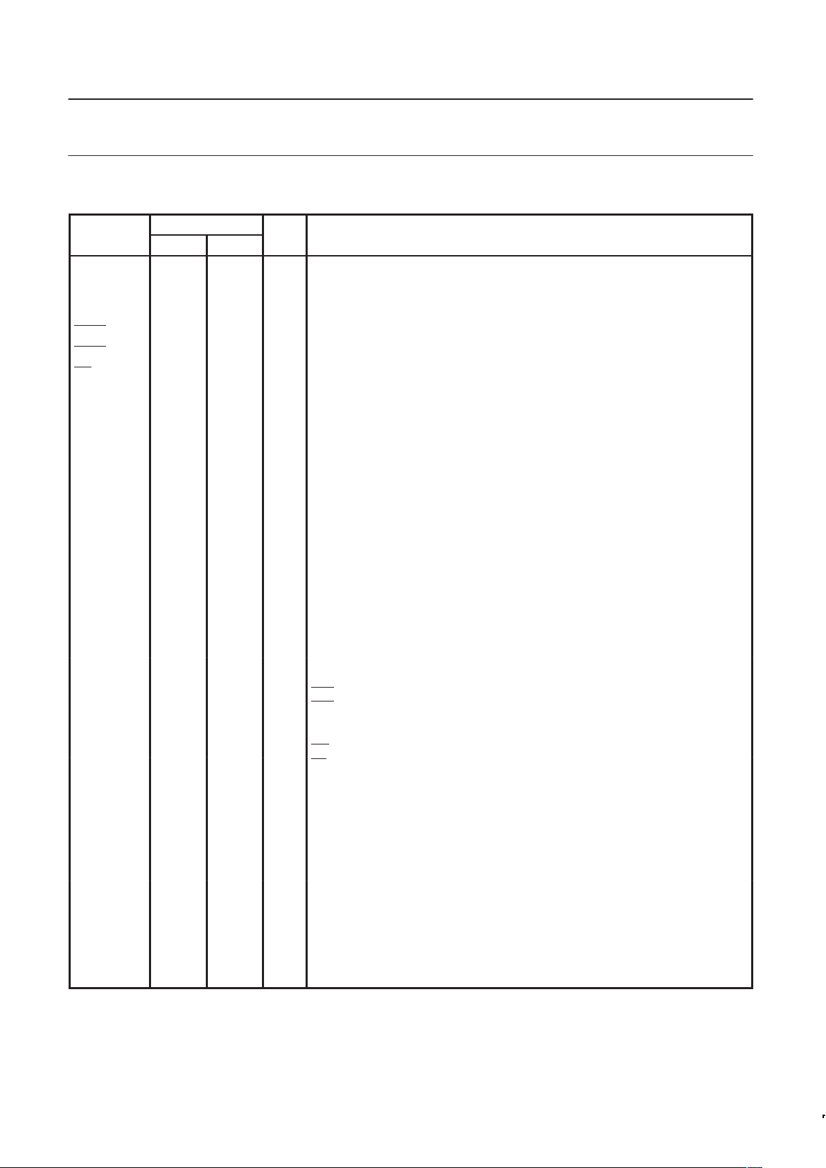
PIN DESCRIPTION
PIN NO.
MNEMONIC PLCC QFP TYPE NAME AND FUNCTION
V
DD
2 72 I Digital Power Supply: +5V power supply pin during normal operation, idle and
power-down mode.
STADC 3 74 I Start ADC Operation: Input starting analog to digital conversion (ADC operation can also
be started by software). This pin must not float.
PWM0 4 75 O Pulse Width Modulation: Output 0.
PWM1 5 76 O Pulse Width Modulation: Output 1.
EW 6 77 I Enable Watchdog Timer: Enable for T3 watchdog timer and disable power-down mode.
This pin must not float.
P0.0-P0.7 57-50 58-51 I/O Port 0: Port 0 is an 8-bit open-drain bidirectional I/O port. Port 0 pins that have 1s written
to them float and can be used as high-impedance inputs. Port 0 is also the multiplexed
low-order address and data bus during accesses to external program and data memory. In
this application it uses strong internal pull-ups when emitting 1s.
P1.0-P1.7 16-23 10-17 I/O Port 1: 8-bit I/O port. Alternate functions include:
16-21 10-15 I/O (P1.0-P1.5): Quasi-bidirectional port pins.
22-23 16-17 I/O (P1.6, P1.7): Open drain port pins.
16-19 10-13 I CT0I-CT3I (P1.0-P1.3): Capture timer input signals for timer T2.
20 14 I T2 (P1.4): T2 event input.
21 15 I RT2 (P1.5): T2 timer reset signal. Rising edge triggered.
22 16 I/O SCL (P1.6): Serial port clock line I2C-bus.
23 17 I/O SDA (P1.7): Serial port data line I2C-bus.
Port 1 is also used to input the lower order address byte during EPROM programming and
verification. A0 is on P1.0, etc.
P2.0-P2.7 39-46 38-42,
45-47
I/O Port 2: 8-bit quasi-bidirectional I/O port.
Alternate function: High-order address byte for external memory (A08-A15).
P3.0-P3.7 24-31 18-20,
23-27
I/O Port 3: 8-bit quasi-bidirectional I/O port. Alternate functions include:
24 18 RxD(P3.0): Serial input port.
25 19 TxD (P3.1): Serial output port.
26 20 INT0 (P3.2): External interrupt.
27 23 INT1 (P3.3): External interrupt.
28 24 T0 (P3.4): Timer 0 external input.
29 25 T1 (P3.5): Timer 1 external input.
30 26 WR (P3.6): External data memory write strobe.
31 27 RD (P3.7): External data memory read strobe.
P4.0-P4.7 7-14 80, 1-2
4-8
I/O Port 4: 8-bit quasi-bidirectional I/O port. Alternate functions include:
7-12 80, 1-2
4-6
O CMSR0-CMSR5 (P4.0-P4.5): Timer T2 compare and set/reset outputs on a match with
timer T2.
13, 14 7, 8 O CMT0, CMT1 (P4.6, P4.7): Timer T2 compare and toggle outputs on a match with timer T2.
P5.0-P5.7 68-62, 71-64, I Port 5: 8-bit input port.
1 ADC0-ADC7 (P5.0-P5.7): Alternate function: Eight input channels to ADC.
RST 15 9 I/O Reset: Input to reset the 8XC552. It also provides a reset pulse as output when timer T3
overflows.
XTAL1 35 32 I Crystal Input 1: Input to the inverting amplifier that forms the oscillator, and input to the
internal clock generator. Receives the external clock signal when an external oscillator is
used.
XTAL2 34 31 O Crystal Input 2: Output of the inverting amplifier that forms the oscillator. Left open-circuit
when an external clock is used.
Philips Semiconductors Product specification
80C552/83C552
Single-chip 8-bit microcontroller
1998 Aug 13
8
PIN DESCRIPTION (Continued)
PIN NO.
MNEMONIC PLCC QFP TYPE NAME AND FUNCTION
V
SS
36, 37 34-36 I Two Digital ground pins.
PSEN 47 48 O Program Store Enable: Active-low read strobe to external program memory.
ALE 48 49 O Address Latch Enable: Latches the low byte of the address during accesses to external
memory. It is activated every six oscillator periods. During an external data memory
access, one ALE pulse is skipped. ALE can drive up to eight LS TTL inputs and handles
CMOS inputs without an external pull-up.
EA 49 50 I External Access: When EA is held at TTL level high, the CPU executes out of the internal
program ROM provided the program counter is less than 8192. When EA
is held at TTL
low level, the CPU executes out of external program memory. EA is not allowed to float.
AV
REF–
58 59 I Analog to Digital Conversion Reference Resistor: Low-end.
AV
REF+
59 60 I Analog to Digital Conversion Reference Resistor: High-end.
AV
SS
60 61 I Analog Ground
AV
DD
61 63 I Analog Power Supply
NOTE:
1. To avoid “latch-up” effect at power-on, the voltage on any pin at any time must not be higher or lower than V
DD
+ 0.5V or VSS – 0.5V ,
respectively.
OSCILLATOR
CHARACTERISTICS
XTAL1 and XTAL2 are the input and output,
respectively, of an inverting amplifier. The
pins can be configured for use as an on-chip
oscillator, as shown in the logic symbol,
page 2.
To drive the device from an external clock
source, XTAL1 should be driven while XTAL2
is left unconnected. There are no
requirements on the duty cycle of the
external clock signal, because the input to
the internal clock circuitry is through a
divide-by-two flip-flop. However, minimum
and maximum high and low times specified in
the data sheet must be observed.
RESET
A reset is accomplished by holding the RST
pin high for at least two machine cycles (24
oscillator periods), while the oscillator is
running. To insure a good power-on reset, the
RST pin must be high long enough to allow
the oscillator time to start up (normally a few
milliseconds) plus two machine cycles. At
power-on, the voltage on V
DD
and RST must
come up at the same time for a proper
start-up.
IDLE MODE
In the idle mode, the CPU puts itself to sleep
while some of the on-chip peripherals stay
active. The instruction to invoke the idle
mode is the last instruction executed in the
normal operating mode before the idle mode
is activated. The CPU contents, the on-chip
RAM, and all of the special function registers
remain intact during this mode. The idle
mode can be terminated either by any
enabled interrupt (at which time the process
is picked up at the interrupt service routine
and continued), or by a hardware reset which
starts the processor in the same manner as a
power-on reset.
POWER-DOWN MODE
In the power-down mode, the oscillator is
stopped and the instruction to invoke
power-down is the last instruction executed.
Only the contents of the on-chip RAM are
preserved. A hardware reset is the only way
to terminate the power-down mode. The
control bits for the reduced power modes are
in the special function register PCON. Table 1
shows the state of the I/O ports during low
current operating modes.
ROM CODE PROTECTION
(83C552)
The 83C552 has an additional security
feature. ROM code protection may be
selected by setting a mask–programmable
security bit (i.e., user dependent). This
feature may be requested during ROM code
submission. When selected, the ROM code
is protected and cannot be read out at any
time by any test mode or by any instruction in
the external program memory space.
The MOVC instructions are the only
instructions that have access to program
code in the internal or external program
memory. The EA
input is latched during
RESET and is “don’t care” after RESET
(also if the security bit is not set). This
implementation prevents reading internal
program code by switching from external
program memory to internal program memory
during a MOVC instruction or any other
instruction that uses immediate data.
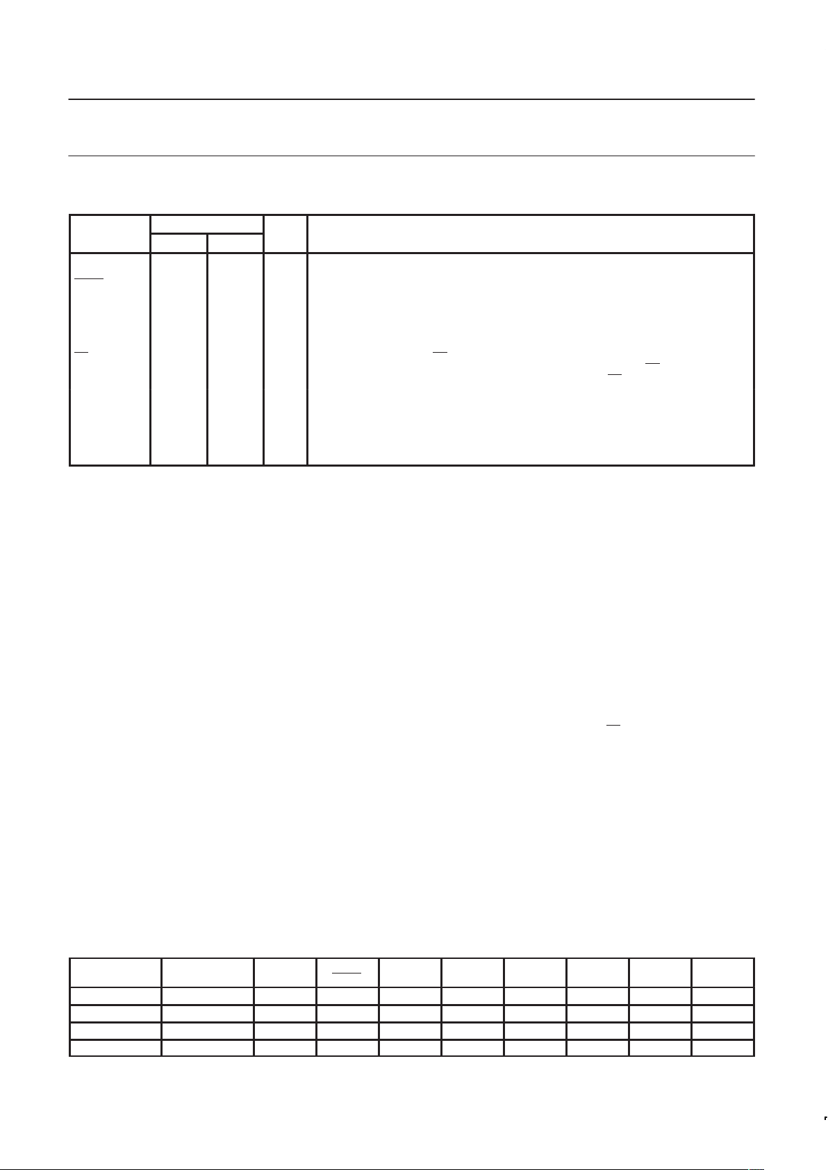
Table 1. External Pin Status During Idle and Power-Down Modes
MODE
PROGRAM
MEMORY
ALE PSEN PORT 0 PORT 1 PORT 2 PORT 3 PORT 4
PWM0/
PWM1
Idle Internal 1 1 Data Data Data Data Data 1
Idle External 1 1 Float Data Address Data Data 1
Power-down Internal 0 0 Data Data Data Data Data 1
Power-down External 0 0 Float Data Data Data Data 1
 Loading...