

Philips P51XAG30KBA, P51XAG30KFA, P51XAG30KFBD Datasheet

INTEGRATED CIRCUITS
XA-G3
XA 16-bit microcontroller family
32K/512 OTP/ROM/ROMless, watchdog, 2 UARTs
Product specification
Supersedes data of 1998 Aug 14
IC25 Data Handbook
1999 Apr 07

Philips Semiconductors Product specification
XA 16-bit microcontroller family
32K/512 OTP/ROM/ROMless, watchdog, 2 UARTs
FAMILY DESCRIPTION
The Philips Semiconductors XA (eXtended Architecture) family of
16-bit single-chip microcontrollers is powerful enough to easily
handle the requirements of high performance embedded
applications, yet inexpensive enough to compete in the market for
high-volume, low-cost applications.
The XA family provides an upward compatibility path for 80C51
users who need higher performance and 64k or more of program
memory. Existing 80C51 code can also easily be translated to run
on XA microcontrollers.
The performance of the XA architecture supports the
comprehensive bit-oriented operations of the 80C51 while
incorporating support for multi-tasking operating systems and
high-level languages such as C. The speed of the XA architecture,
at 10 to 100 times that of the 80C51, gives designers an easy path
to truly high performance embedded control.
The XA architecture supports:
•Upward compatibility with the 80C51 architecture
•16-bit fully static CPU with a 24-bit program and data address
range
•Eight 16-bit CPU registers each capable of performing all
arithmetic and logic operations as well as acting as memory
pointers. Operations may also be performed directly to memory.
•Both 8-bit and 16-bit CPU registers, each capable of performing
all arithmetic and logic operations.
•An enhanced instruction set that includes bit intensive logic
operations and fast signed or unsigned 16 × 16 multiply and
32 / 16 divide
XA-G3
•Instruction set tailored for high level language support
•Multi-tasking and real-time executives that include up to 32
vectored interrupts, 16 software traps, segmented data memory,
and banked registers to support context switching
•Low power operation, which is intrinsic to the XA architecture,
includes power-down and idle modes.
More detailed information on the core is available in the XA User
Guide.
SPECIFIC FEATURES OF THE XA-G3
•20-bit address range, 1 megabyte each program and data space.
(Note that the XA architecture supports up to 24 bit addresses.)
•2.7V to 5.5V operation
•32K bytes on-chip EPROM/ROM program memory =
XA-G37/XA-G33
•512 bytes of on-chip data RAM
•Three counter/timers with enhanced features
(equivalent to 80C51 T0, T1, and T2)
•Watchdog timer
•Two enhanced UARTs
•Four 8-bit I/O ports with 4 programmable output configurations
•44-pin PLCC and 44-pin LQFP packages
ORDERING INFORMATION
ROMless ROM EPROM
P51XAG30KB BD P51XAG33KB BD PXAG37KB BD OTP 0 to +70, Plastic Low Profile Quad Flat Pkg. 30 SOT389–1
P51XAG30KB A P51XAG33KB A PXAG37KB A OTP 0 to +70, Plastic Leaded Chip Carrier 30 SOT187–2
P51XAG30KF BD P51XAG33KF BD PXAG37KF BD OTP –40 to +85, Plastic Low Profile Quad Flat Pkg. 30 SOT389–1
P51XAG30KF A P51XAG33KF A PXAG37KF A OTP –40 to +85, Plastic Leaded Chip Carrier 30 SOT187–2
NOTE:
1. OTP = One Time Programmable EPROM. UV = Erasable EPROM.
1
TEMPERATURE RANGE °C AND PACKAGE
FREQ
(MHz)
DRAWING
NUMBER
1999 Apr 07 853-2052 21197
2
Philips Semiconductors Product specification
XA 16-bit microcontroller family
32K/512 OTP/ROM/ROMless, watchdog, 2 UARTs
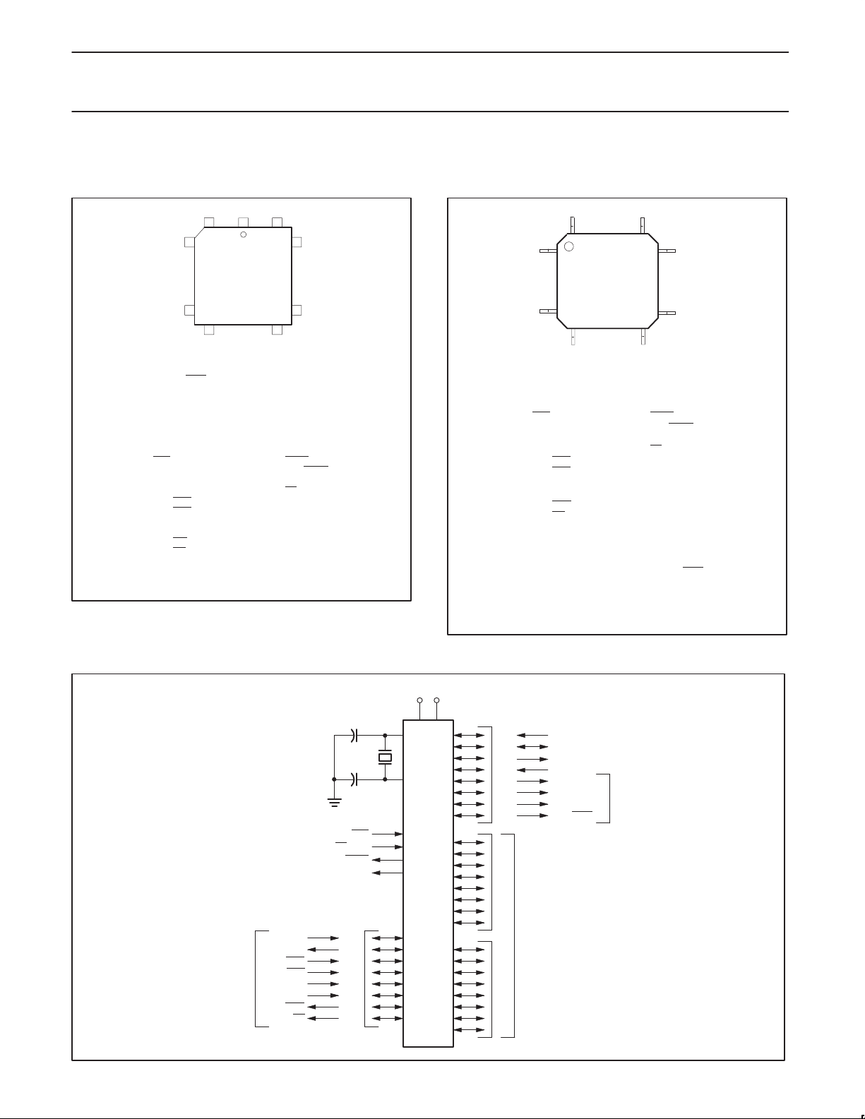
PIN CONFIGURATIONS
44-Pin PLCC Package
6140
7
17
Pin Function
1V
SS
2 P1.0/A0/WRH
3 P1.1/A1
4 P1.2/A2
5 P1.3/A3
6 P1.4/RxD1
7 P1.5/TxD1
8 P1.6/T2
9 P1.7/T2EX
10 RST
11 P3.0/RxD0
12 NC
13 P3.1/TxD0
14 P3.2/INT0
15 P3.3/INT1
16 P3.4/T0
17 P3.5/T1/BUSW
18 P3.6/WR
19 P3.7/RD
20 XTAL2
21 XTAL1
22 V
L
SS
PLCC
18 28
Pin Function
23 V
24 P2.0/A12D8
25 P2.1/A13D9
26 P2.2/A14D10
27 P2.3/A15D11
28 P2.4/A16D12
29 P2.5/A17D13
30 P2.6/A18D14
31 P2.7/A19D15
32 PSEN
33 ALE/PROG
34 NC
35 EA
36 P0.7/A11D7
37 P0.6/A10D6
38 P0.5/A9D5
39 P0.4/A8D4
40 P0.3/A7D3
41 P0.2/A6D2
42 P0.1/A5D1
43 P0.0/A4D0
44 V
39
29
DD
/VPP/WAIT
DD
SU00525
44-Pin LQFP Package
44 34
1
11
12 22
Pin Function
1 P1.5/TxD1
2 P1.6/T2
3 P1.7/T2EX
4 RST
5 P3.0/RxD0
6NC
7 P3.1/TxD0
8 P3.2/INT0
9 P3.3/INT1
10 P3.4/T0
11 P3.5/T1/BUSW
12 P3.6/WRL
13 P3.7/RD
14 XTAL2
15 XTAL1
16 V
SS
17 V
DD
18 P2.0/A12D8
19 P2.1/A13D9
20 P2.2/A14D10
21 P2.3/A15D11
22 P2.4/A16/D12
LQFP
Pin Function
23 P2.5/A17D13
24 P2.6/A18D14
25 P2.7/A19D15
26 PSEN
27 ALE/PROG
28 NC
29 EA
30 P0.7/A11D7
31 P0.6/A10D6
32 P0.5/A9D5
33 P0.4/A8D4
34 P0.3/A7D3
35 P0.2/A6D2
36 P0.1/A5D1
37 P0.0/A4D0
38 V
39 V
40 P1.0/A0/WRH
41 P1.1/A1
42 P1.2/A2
43 P1.3/A3
44 P1.4/RxD1
/VPP/WAIT
DD
SS
SU00580
XA-G3
33
23
LOGIC SYMBOL
* NOT AVAILABLE ON 40-PIN DIP PACKAGE
RxD0
TxD0
INT0
INT1
T0
T1/BUSW
WRL
ALTERNATE FUNCTIONS
RD
RST
EA/WAIT
PSEN
ALE
VDDV
SS
XTAL1
XTAL2
PORT 3
PORT 1PORT 2
PORT 0
ADDRESS AND DATA BUS
T2EX*
T2*
TXD1
D1
R
X
A3
A2
A1
A0/WRH
BUS
ADDRESS
SU00526
1999 Apr 07
3

Philips Semiconductors Product specification
XA 16-bit microcontroller family
32K/512 OTP/ROM/ROMless, watchdog, 2 UARTs
BLOCK DIAGRAM
XA CPU Core
Program
Memory
Bus
32K BYTES
ROM/EPROM
512 BYTES
STATIC RAM
PORT 0
Data Bus
XA-G3
SFR BUS
UART0
UART1
PORT 1
PORT 2
PORT 3
TIMER 0 &
TIMER 1
TIMER 2
WATCHDOG
TIMER
SU00527
1999 Apr 07
4

Philips Semiconductors Product specification
MNEMONIC
TYPE
NAME AND FUNCTION
XA 16-bit microcontroller family
XA-G3
32K/512 OTP/ROM/ROMless, watchdog, 2 UARTs
PIN DESCRIPTIONS
PIN. NO.
PLCC LQFP
V
SS
V
DD
P0.0 – P0.7 43–36 37–30 I/O Port 0: Port 0 is an 8-bit I/O port with a user-configurable output type. Port 0 latches have 1s
P1.0 – P1.7 2–9 40–44,
P2.0 – P2.7 24–31 18–25 I/O Port 2: Port 2 is an 8-bit I/O port with a user-configurable output type. Port 2 latches have 1s
P3.0 – P3.7 11,
RST 10 4 I Reset: A low on this pin resets the microcontroller, causing I/O ports and peripherals to take on
ALE/PROG 33 27 I/O Address Latch Enable/Program Pulse: A high output on the ALE pin signals external circuitry to
1, 22 16 I Ground: 0V reference.
23, 44 17 I Power Supply: This is the power supply voltage for normal, idle, and power down operation.
written to them and are configured in the quasi-bidirectional mode during reset. The operation of
port 0 pins as inputs and outputs depends upon the port configuration selected. Each port pin is
configured independently. Refer to the section on I/O port configuration and the DC Electrical
Characteristics for details.
When the external program/data bus is used, Port 0 becomes the multiplexed low data/instruction
byte and address lines 4 through 11.
1–3
2 40 O A0/WRH: Address bit 0 of the external address bus when the external data bus is
3 41 O A1: Address bit 1 of the external address bus.
4 42 O A2: Address bit 2 of the external address bus.
5 43 O A3: Address bit 3 of the external address bus.
6 44 I RxD1 (P1.4): Receiver input for serial port 1.
7 1 O TxD1 (P1.5): Transmitter output for serial port 1.
8 2 I/O T2 (P1.6): T imer/counter 2 external count input/clockout.
9 3 I T2EX (P1.7): Timer/counter 2 reload/capture/direction control
13–195,7–13
11 5 I RxD0 (P3.0): Receiver input for serial port 0.
13 7 O TxD0 (P3.1): Transmitter output for serial port 0.
14 8 I INT0 (P3.2): External interrupt 0 input.
15 9 I INT1 (P3.3): External interrupt 1 input.
16 10 I/O T0 (P3.4): Timer 0 external input, or timer 0 overflow output.
17 11 I/O T1/BUSW (P3.5): Timer 1 external input, or timer 1 overflow output. The value on this pin is
18 12 O WRL (P3.6): External data memory low byte write strobe.
19 13 O RD (P3.7): External data memory read strobe.
I/O Port 1: Port 1 is an 8-bit I/O port with a user-configurable output type. Port 1 latches have 1s
written to them and are configured in the quasi-bidirectional mode during reset. The operation of
port 1 pins as inputs and outputs depends upon the port configuration selected. Each port pin is
configured independently. Refer to the section on I/O port configuration and the DC Electrical
Characteristics for details.
Port 1 also provides special functions as described below.
configured for an 8 bit width. When the external data bus is configured for a 16
bit width, this pin becomes the high byte write strobe.
written to them and are configured in the quasi-bidirectional mode during reset. The operation of
port 2 pins as inputs and outputs depends upon the port configuration selected. Each port pin is
configured independently. Refer to the section on I/O port configuration and the DC Electrical
Characteristics for details.
When the external program/data bus is used in 16-bit mode, Port 2 becomes the multiplexed high
data/instruction byte and address lines 12 through 19. When the external program/data bus is used in
8-bit mode, the number of address lines that appear on port 2 is user programmable.
I/O Port 3: Port 3 is an 8-bit I/O port with a user configurable output type. Port 3 latches have 1s
written to them and are configured in the quasi-bidirectional mode during reset. the operation of
port 3 pins as inputs and outputs depends upon the port configuration selected. Each port pin is
configured independently. Refer to the section on I/O port configuration and the DC Electrical
Characteristics for details.
Port 3 also provides various special functions as described below.
latched as the external reset input is released and defines the default
external data bus width (BUSW). 0 = 8-bit bus and 1 = 16-bit bus.
their default states, and the processor to begin execution at the address contained in the reset
vector. Refer to the section on Reset for details.
latch the address portion of the multiplexed address/data bus. A pulse on ALE occurs only when it
is needed in order to process a bus cycle.
1999 Apr 07
5

Philips Semiconductors Product specification
SFR
NAME
DESCRIPTION
SFR
XA 16-bit microcontroller family
XA-G3
32K/512 OTP/ROM/ROMless, watchdog, 2 UARTs
MNEMONIC NAME AND FUNCTIONTYPE
MNEMONIC NAME AND FUNCTIONTYPE
PSEN 32 26 O Program Store Enable: The read strobe for external program memory. When the microcontroller
EA/WAIT/
V
PP
XTAL1 21 15 I Crystal 1: Input to the inverting amplifier used in the oscillator circuit and input to the internal clock
XTAL2 20 14 O Crystal 2: Output from the oscillator amplifier.
SPECIAL FUNCTION REGISTERS
PIN. NO.
LQFPPLCC
accesses external program memory, PSEN
is only active when external code accesses are performed.
35 29 I External Access/Wait: The EA input determines whether the internal program memory of the
microcontroller is used for code execution. The value on the EA pin is latched as the external reset
input is released and applies during later execution. When latched as a 0, external program
memory is used exclusively, when latched as a 1, internal program memory will be used up to its
limit, and external program memory used above that point. After reset is released, this pin takes on
the function of bus Wait input. If Wait is asserted high during any external bus access, that cycle
will be extended until Wait is released. During EPROM programming, this pin is also the
programming supply voltage input.
generator circuits.
BIT FUNCTIONS AND ADDRESSES
ADDRESS
MSB LSB
is driven low in order to enable memory devices. PSEN
RESET
VALUE
BCR Bus configuration register 46A — — — WAITD BUSD BC2 BC1 BC0 Note 1
BTRH Bus timing register high byte 469 DW1 DW0 DWA1 DWA0 DR1 DR0 DRA1 DRA0 FF
BTRL Bus timing register low byte 468 WM1 WM0 ALEW — CR1 CR0 CRA1 CRA0 EF
CS Code segment 443 00
DS Data segment 441 00
ES Extra segment 442 00
33F 33E 33D 33C 33B 33A 339 338
IEH* Interrupt enable high byte 427 — — — — ETI1 ERI1 ETI0 ERI0 00
337 336 335 334 333 332 331 330
IEL* Interrupt enable low byte 426 EA — — ET2 ET1 EX1 ET0 EX0 00
IPA0 Interrupt priority 0 4A0 — PT0 — PX0 00
IPA1 Interrupt priority 1 4A1 — PT1 — PX1 00
IPA2 Interrupt priority 2 4A2 — — — PT2 00
IPA4 Interrupt priority 4 4A4 — PTI0 — PRI0 00
IPA5 Interrupt priority 5 4A5 — PTI1 — PRI1 00
387 386 385 384 383 382 381 380
P0* Port 0 430 AD7 AD6 AD5 AD4 AD3 AD2 AD1 AD0 FF
38F 38E 38D 38C 38B 38A 389 388
P1* Port 1 431 T2EX T2 TxD1 RxD1 A3 A2 A1 WRH FF
397 396 395 394 393 392 391 390
P2* Port 2 432 P2.7 P2.6 P2.5 P2.4 P2.3 P2.2 P2.1 P2.0 FF
1999 Apr 07
6
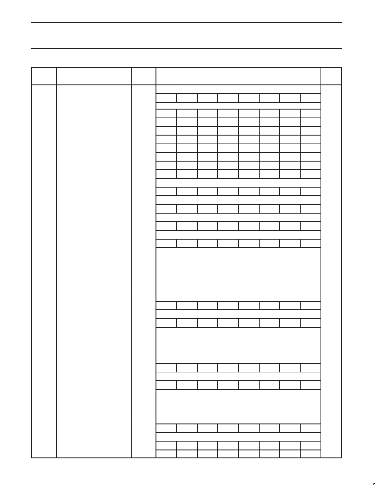
Philips Semiconductors Product specification
XA 16-bit microcontroller family
XA-G3
32K/512 OTP/ROM/ROMless, watchdog, 2 UARTs
SFR
NAME
NAME
P3* Port 3 433 RD WR T1 T0 INT1 INT0 TxD0 RxD0 FF
P0CFGA Port 0 configuration A 470 Note 5
P1CFGA Port 1 configuration A 471 Note 5
P2CFGA Port 2 configuration A 472 Note 5
P3CFGA Port 3 configuration A 473 Note 5
P0CFGB Port 0 configuration B 4F0 Note 5
P1CFGB Port 1 configuration B 4F1 Note 5
P2CFGB Port 2 configuration B 4F2 Note 5
P3CFGB Port 3 configuration B 4F3 Note 5
PCON* Power control register 404 — — — — — — PD IDL 00
PSWH* Program status word (high byte) 401 SM TM RS1 RS0 IM3 IM2 IM1 IM0 Note 2
PSWL* Program status word (low byte) 400 C AC — — — V N Z Note 2
PSW51* 80C51 compatible PSW 402 C AC F0 RS1 RS0 V F1 P Note 3
DESCRIPTION
DESCRIPTION
SFR
ADDRESS
ADDRESS
39F 39E 39D 39C 39B 39A 399 398
227 226 225 224 223 222 221 220
20F 20E 20D 20C 20B 20A 209 208
207 206 205 204 203 202 201 200
217 216 215 214 213 212 211 210
BIT FUNCTIONS AND ADDRESSES
RESET
RESET
VALUE
VALUE
LSBMSB
RTH0 Timer 0 extended reload,
high byte
RTH1 Timer 1 extended reload,
high byte
RTL0 Timer 0 extended reload, low byte 454 00
RTL1 Timer 1 extended reload, low byte 456 00
S0CON* Serial port 0 control register 420 SM0_0 SM1_0 SM2_0 REN_0 TB8_0 RB8_0 TI_0 RI_0 00
S0STAT* Serial port 0 extended status 421 — — — — FE0 BR0 OE0
S0BUF Serial port 0 buffer register 460 x
S0ADDR Serial port 0 address register 461 00
S0ADEN Serial port 0 address enable
register
S1CON* Serial port 1 control register 424 SM0_1 SM1_1 SM2_1 REN_1 TB8_1 RB8_1 TI_1 RI_1 00
S1STAT* Serial port 1 extended status 425 — — — — FE1 BR1 OE1
S1BUF Serial port 1 buffer register 464 x
S1ADDR Serial port 1 address register 465 00
S1ADEN Serial port 1 address enable
register
SCR System configuration register 440 — — — — PT1 PT0 CM PZ 00
SSEL* Segment selection register 403
SWE Software Interrupt Enable 47A — SWE7 SWE6 SWE5 SWE4 SWE3 SWE2 SWE1 00
455 00
457 00
307 306 305 304 303 302 301 300
30F 30E 30D 30C 30B 30A 309 308
STINT0
462 00
327 326 325 324 323 322 321 320
32F 32E 32D 32C 32B 32A 329 328
STINT1
466 00
21F 21E 21D 21C 21B 21A 219 218
ESWEN
R6SEG R5SEG R4SEG R3SEG R2SEG R1SEG R0SEG
00
00
00
1999 Apr 07
7

Philips Semiconductors Product specification
XA 16-bit microcontroller family
XA-G3
32K/512 OTP/ROM/ROMless, watchdog, 2 UARTs
SFR
NAME
NAME
SWR* Software Interrupt Request 42A — SWR7 SWR6 SWR5 SWR4 SWR3 SWR2 SWR1 00
T2CON* Timer 2 control register 418 TF2 EXF2 RCLK0 TCLK0
T2MOD* Timer 2 mode control 419 — — RCLK1 TCLK1 — — T2OE DCEN 00
TH2 Timer 2 high byte 459 00
TL2 T imer 2 low byte 458 00
T2CAPH Timer 2 capture register,
T2CAPL Timer 2 capture register,
TCON* Timer 0 and 1 control register 410 TF1 TR1 TF0 TR0 IE1 IT1 IE0 IT0 00
TH0 Timer 0 high byte 451 00
TH1 Timer 1 high byte 453 00
TL0 T imer 0 low byte 450 00
TL1 T imer 1 low byte 452 00
TMOD Timer 0 and 1 mode control 45C GATE C/T M1 M0 GATE C/T M1 M0 00
TSTAT* Timer 0 and 1 extended status 411 — — — — — T1OE — T0OE 00
WDCON*
WDL Watchdog timer reload 45F 00
WFEED1
WFEED2
NOTES:
* SFRs are bit addressable.
1. At reset, the BCR register is loaded with the binary value 0000 0a11, where “a” is the value on the BUSW pin. This defaults the address bus
size to 20 bits since the XA-G3 has only 20 address lines.
2. SFR is loaded from the reset vector.
3. All bits except F1, F0, and P are loaded from the reset vector. Those bits are all 0.
4. Unimplemented bits in SFRs are X (unknown) at all times. Ones should not be written to these bits since they may be used for other
purposes in future XA derivatives. The reset value shown for these bits is 0.
5. Port configurations default to quasi-bidirectional when the XA begins execution from internal code memory after reset, based on the
condition found on the EA pin. Thus all PnCFGA registers will contain FF and PnCFGB registers will contain 00. When the XA begins
execution using external code memory, the default configuration for pins that are associated with the external bus will be push-pull. The
PnCFGA and PnCFGB register contents will reflect this difference.
6. The WDCON reset value is E6 for a Watchdog reset, E4 for all other reset causes.
7. The XA-G3 implements an 8-bit SFR bus, as stated in Chapter 8 of the
write 16 bits to an SFR will actually write only the lower 8 bits. Sixteen bit SFR reads will return undefined data in the upper byte.
DESCRIPTION
DESCRIPTION
high byte
low byte
Watchdog control register 41F PRE2 PRE1 PRE0 — —
Watchdog feed 1 45D x
Watchdog feed 2 45E x
SFR
ADDRESS
ADDRESS
357 356 355 354 353 352 351 350
2C7 2C6 2C5 2C4 2C3 2C2 2C1 2C0
2CF 2CE 2CD 2CC 2CB 2CA 2C9 2C8
45B 00
45A 00
287 286 285 284 283 282 281 280
28F 28E 28D 28C 28B 28A 289 288
2FF 2FE 2FD 2FC 2FB 2FA 2F9 2F8
BIT FUNCTIONS AND ADDRESSES
EXEN2
XA User Guide
. All SFR accesses must be 8-bit operations. Attempts to
TR2 C/T2
WDRUN WDTOF
CP/RL2
RESET
RESET
VALUE
VALUE
LSBMSB
00
—
Note 6
1999 Apr 07
8

Philips Semiconductors Product specification
XA 16-bit microcontroller family
32K/512 OTP/ROM/ROMless, watchdog, 2 UARTs
XA-G3 TIMER/COUNTERS
The XA has two standard 16-bit enhanced Timer/Counters: Timer 0
and Timer 1. Additionally, it has a third 16-bit Up/Down
timer/counter, T2. A central timing generator in the XA core provides
the time-base for all XA Timers and Counters. The timer/event
counters can perform the following functions:
– Measure time intervals and pulse duration
– Count external events
– Generate interrupt requests
– Generate PWM or timed output waveforms
All of the timer/counters (Timer 0, Timer 1 and Timer 2) can be
independently programmed to operate either as timers or event
counters via the C/T bit in the TnCON register. All timers count up
unless otherwise stated. These timers may be dynamically read
during program execution.
The base clock rate of all of the timers is user programmable. This
applies to timers T0, T1, and T2 when running in timer mode (as
opposed to counter mode), and the watchdog timer. The clock
driving the timers is called TCLK and is determined by the setting of
two bits (PT1, PT0) in the System Configuration Register (SCR).
The frequency of TCLK may be selected to be the oscillator input
divided by 4 (Osc/4), the oscillator input divided by 16 (Osc/16), or
the oscillator input divided by 64 (Osc/64). This gives a range of
possibilities for the XA timer functions, including baud rate
XA-G3
generation, Timer 2 capture. Note that this single rate setting applies
to all of the timers.
When timers T0, T1, or T2 are used in the counter mode, the
register will increment whenever a falling edge (high to low
transition) is detected on the external input pin corresponding to the
timer clock. These inputs are sampled once every 2 oscillator
cycles, so it can take as many as 4 oscillator cycles to detect a
transition. Thus the maximum count rate that can be supported is
Osc/4. The duty cycle of the timer clock inputs is not important, but
any high or low state on the timer clock input pins must be present
for 2 oscillator cycles before it is guaranteed to be “seen” by the
timer logic.
Timer 0 and Timer 1
The “Timer” or “Counter” function is selected by control bits C/T in
the special function register TMOD. These two Timer/Counters have
four operating modes, which are selected by bit-pairs (M1, M0) in
the TMOD register. T imer modes 1, 2, and 3 in XA are kept identical
to the 80C51 timer modes for code compatibility. Only the mode 0 is
replaced in the XA by a more powerful 16-bit auto-reload mode. This
will give the XA timers a much larger range when used as time
bases.
The recommended M1, M0 settings for the different modes are
shown in Figure 2.
SCR Address:440
Not Bit Addressable
Reset Value: 00H
PT1 PT0 OPERATING
0 0 Osc/4
0 1 Osc/16
1 0 Osc/64
1 1 Reserved
CM Compatibility Mode allows the XA to execute most translated 80C51 code on the XA. The
PZ Page Zero mode forces all program and data addresses to 16-bits only. This saves stack space
TMOD Address:45C
Not Bit Addressable
Reset Value: 00H
GATE Gating control when set. Timer/Counter “n” is enabled only while “INTn” pin is high and
C/T Timer or Counter Selector cleared for Timer operation (input from internal system clock.)
M1 M0 OPERATING
0 0 16-bit auto-reload timer/counter
0 1 16-bit non-auto-reload timer/counter
1 0 8-bit auto-reload timer/counter
1 1 Dual 8-bit timer mode (timer 0 only)
———
Prescaler selection.
XA register file must copy the 80C51 mapping to data memory and mimic the 80C51 indirect
addressing scheme.
and speeds up execution but limits memory access to 64k.
Figure 1. System Configuration Register (SCR)
GATE C/T M1
TIMER 1 TIMER 0
“TRn” control bit is set. When cleared Timer “n” is enabled whenever “TRn” control bit is set.
Set for Counter operation (input from “Tn” input pin).
Figure 2. Timer/Counter Mode Control (TMOD) Register
— PT1 PT0 CM PZ
M0 GATE C/T
M1 M0
LSBMSB
LSBMSB
SU00589
SU00605
1999 Apr 07
9

Philips Semiconductors Product specification
XA 16-bit microcontroller family
32K/512 OTP/ROM/ROMless, watchdog, 2 UARTs
New Enhanced Mode 0
For timers T0 or T1 the 13-bit count mode on the 80C51 (current
Mode 0) has been replaced in the XA with a 16-bit auto-reload
mode. Four additional 8-bit data registers (two per timer: RTHn and
RTLn) are created to hold the auto-reload values. In this mode, the
TH overflow will set the TF flag in the TCON register and cause both
the TL and TH counters to be loaded from the RTL and RTH
registers respectively.
These new SFRs will also be used to hold the TL reload data in the
8-bit auto-reload mode (Mode 2) instead of TH.
The overflow rate for Timer 0 or Timer 1 in Mode 0 may be
calculated as follows:
Timer_Rate = Osc / (N * (65536 – Timer_Reload_Value))
where N = the TCLK prescaler value: 4 (default), 16, or 64.
Mode 1
Mode 1 is the 16-bit non-auto reload mode.
Mode 2
Mode 2 configures the Timer register as an 8-bit Counter (TLn) with
automatic reload. Overflow from TLn not only sets TFn, but also
reloads TLn with the contents of RTLn, which is preset by software.
The reload leaves THn unchanged.
XA-G3
Mode 2 operation is the same for Timer/Counter 0.
The overflow rate for Timer 0 or Timer 1 in Mode 2 may be
calculated as follows:
Timer_Rate = Osc / (N * (256 – Timer_Reload_Value))
where N = the TCLK prescaler value: 4, 16, or 64.
Mode 3
Timer 1 in Mode 3 simply holds its count. The effect is the same as
setting TR1 = 0.
Timer 0 in Mode 3 establishes TL0 and TH0 as two separate
counters. TL0 uses the Timer 0 control bits: C/T, GA TE, TR0, INT0,
and TF0. TH0 is locked into a timer function and takes over the use
of TR1 and TF1 from Timer 1. Thus, TH0 now controls the “Timer 1”
interrupt.
Mode 3 is provided for applications requiring an extra 8-bit timer.
When Timer 0 is in Mode 3, Timer 1 can be turned on and of f by
switching it out of and into its own Mode 3, or can still be used by
the serial port as a baud rate generator, or in fact, in any application
not requiring an interrupt.
TCON Address:410
Bit Addressable
Reset Value: 00H
BIT SYMBOL FUNCTION
TCON.7 TF1 Timer 1 overflow flag. Set by hardware on Timer/Counter overflow.
This flag will not be set if T1OE (TSTAT.2) is set.
Cleared by hardware when processor vectors to interrupt routine, or by clearing the bit in software.
TCON.6 TR1 Timer 1 Run control bit. Set/cleared by software to turn Timer/Counter 1 on/off.
TCON.5 TF0 Timer 0 overflow flag. Set by hardware on Timer/Counter overflow.
This flag will not be set if T0OE (TSTAT.0) is set.
Cleared by hardware when processor vectors to interrupt routine, or by clearing the bit in software.
TCON.4 TR0 Timer 0 Run control bit. Set/cleared by software to turn Timer/Counter 0 on/off.
TCON.3 IE1 Interrupt 1 Edge flag. Set by hardware when external interrupt edge detected.
Cleared when interrupt processed.
TCON.2 IT1 Interrupt 1 type control bit. Set/cleared by software to specify falling edge/low level triggered
external interrupts.
TCON.1 IE0 Interrupt 0 Edge flag. Set by hardware when external interrupt edge detected.
Cleared when interrupt processed.
TCON.0 IT0 Interrupt 0 Type control bit. Set/cleared by software to specify falling edge/low level
triggered external interrupts.
Figure 3. Timer/Counter Control (TCON) Register
IE0IT1IE1TR0TF0TR1TF1
LSBMSB
IT0
SU00604C
1999 Apr 07
10

Philips Semiconductors Product specification
XA 16-bit microcontroller family
32K/512 OTP/ROM/ROMless, watchdog, 2 UARTs
T2CON Address:418
Bit Addressable
Reset Value: 00H
BIT SYMBOL FUNCTION
T2CON.7 TF2 Timer 2 overflow flag. Set by hardware on Timer/Counter overflow. Must be cleared by software.
TF2 will not be set when RCLK0, RCLK1, TCLK0, TCLK1 or T2OE=1.
T2CON.6 EXF2 Timer 2 external flag is set when a capture or reload occurs due to a negative transition on T2EX (and
EXEN2 is set). This flag will cause a Timer 2 interrupt when this interrupt is enabled. EXF2 is cleared by
software.
T2CON.5 RCLK0 Receive Clock Flag.
T2CON.4 TCLK0 Transmit Clock Flag. RCLK0 and TCLK0 are used to select Timer 2 overflow rate as a clock source for
UART0 instead of Timer T1.
T2CON.3 EXEN2 Timer 2 external enable bit allows a capture or reload to occur due to a negative transition on T2EX.
T2CON.2 TR2 Start=1/Stop=0 control for Timer 2.
T2CON.1 C/T2 Timer or counter select.
0=Internal timer
1=External event counter (falling edge triggered)
T2CON.0 CP/RL2 Capture/Reload flag.
If CP/RL2 & EXEN2=1 captures will occur on negative transitions of T2EX.
If CP/RL2=0, EXEN2=1 auto reloads occur with either Timer 2 overflows or negative transitions at T2EX.
If RCLK or TCLK=1 the timer is set to auto reload on Timer 2 overflow, this bit has no effect.
Figure 4. Timer/Counter 2 Control (T2CON) Register
C/T2TR2EXEN2TCLK0RCLK0EXF2TF2
LSBMSB
CP/RL2
XA-G3
SU00606A
New Timer-Overflow Toggle Output
In the XA, the timer module now has two outputs, which toggle on
overflow from the individual timers. The same device pins that are
used for the T0 and T1 count inputs are also used for the new
overflow outputs. An SFR bit (TnOE in the TSTAT register) is
associated with each counter and indicates whether Port-SFR data
or the overflow signal is output to the pin. These outputs could be
used in applications for generating variable duty cycle PWM outputs
(changing the auto-reload register values). Also variable frequency
(Osc/8 to Osc/8,388,608) outputs could be achieved by adjusting
the prescaler along with the auto-reload register values. With a
30.0MHz oscillator, this range would be 3.58Hz to 3.75MHz.
Timer T2
Timer 2 in the XA is a 16-bit Timer/Counter which can operate as
either a timer or as an event counter. This is selected by C/T2 in the
special function register T2CON. Upon timer T2 overflow/underflow,
the TF2 flag is set, which may be used to generate an interrupt. It
can be operated in one of three operating modes: auto-reload (up or
down counting), capture, or as the baud rate generator (for either or
both UARTs via SFRs T2MOD and T2CON). These modes are
shown in Table 1.
Capture Mode
In the capture mode there are two options which are selected by bit
EXEN2 in T2CON. If EXEN2 = 0, then timer 2 is a 16-bit timer or
counter, which upon overflowing sets bit TF2, the timer 2 overflow
bit. This will cause an interrupt when the timer 2 interrupt is enabled.
If EXEN2 = 1, then Timer 2 still does the above, but with the added
feature that a 1-to-0 transition at external input T2EX causes the
current value in the Timer 2 registers, TL2 and TH2, to be captured
into registers RCAP2L and RCAP2H, respectively. In addition, the
transition at T2EX causes bit EXF2 in T2CON to be set. This will
cause an interrupt in the same fashion as TF2 when the Timer 2
interrupt is enabled. The capture mode is illustrated in Figure 7.
Auto-Reload Mode (Up or Down Counter)
In the auto-reload mode, the timer registers are loaded with the
16-bit value in T2CAPH and T2CAPL when the count overflows.
T2CAPH and T2CAPL are initialized by software. If the EXEN2 bit in
T2CON is set, the timer registers will also be reloaded and the EXF2
flag set when a 1-to-0 transition occurs at input T2EX. The
auto-reload mode is shown in Figure 8.
In this mode, Timer 2 can be configured to count up or down. This is
done by setting or clearing the bit DCEN (Down Counter Enable) in
the T2MOD special function register (see Table 1). The T2EX pin
then controls the count direction. When T2EX is high, the count is in
the up direction, when T2EX is low, the count is in the down
direction.
Figure 8 shows Timer 2, which will count up automatically, since
DCEN = 0. In this mode there are two options selected by bit
EXEN2 in the T2CON register. If EXEN2 = 0, then Timer 2 counts
up to FFFFH and sets the TF2 (Overflow Flag) bit upon overflow.
This causes the Timer 2 registers to be reloaded with the 16-bit
value in T2CAPL and T2CAPH, whose values are preset by
software. If EXEN2 = 1, a 16-bit reload can be triggered either by an
overflow or by a 1-to-0 transition at input T2EX. This transition also
sets the EXF2 bit. If enabled, either TF2 or EXF2 bit can generate
the Timer 2 interrupt.
In Figure 9, the DCEN = 1; this enables the Timer 2 to count up or
down. In this mode, the logic level of T2EX pin controls the direction
of count. When a logic ‘1’ is applied at pin T2EX, the Timer 2 will
count up. The Timer 2 will overflow at FFFFH and set the TF2 flag,
which can then generate an interrupt if enabled. This timer overflow,
also causes the 16-bit value in T2CAPL and T2CAPH to be
reloaded into the timer registers TL2 and TH2, respectively.
A logic ‘0’ at pin T2EX causes Timer 2 to count down. When
counting down, the timer value is compared to the 16-bit value
contained in T2CAPH and T2CAPL. When the value is equal, the
1999 Apr 07
11
 Loading...