

Philips OQ2538HP Datasheet

INTEGRATED CIRCUITS
DATA SH EET
OQ2538HP
SDH/SONET main amplifier
Preliminary specification
File under Integrated Circuits, IC19
1997 Nov 26
Philips Semiconductors Preliminary specification
SDH/SONET main amplifier OQ2538HP
FEATURES
• Differential 100 Ω outputs for direct connection to
Current-Mode Logic (CML) inputs
• Wide bandwidth (3 GHz)
• 48.5 dB limiting gain
• Noise figure typically 11 dB
• Automatic offset compensation
• Input level-detection circuits for Automatic Gain Control
(AGC) and Loss Of Signal (LOS) detection
• Low power dissipation (typically 270 mW)
• Single −4.5 V supply voltage
• Low cost LQFP48 plastic package.
APPLICATIONS
• Main amplifier in Synchronous Digital Hierarchy (SDH)
and Synchronous Optical Network (SONET) systems for
short, medium and long haul optical transmission
• Level detector for laser diode control loops
• Wideband RF gain block with internal level detectors.
GENERAL DESCRIPTION
The OQ2538HP is a limiting amplifier IC intended for use
as the main amplifier in 2.5 Gbits/s Non-Return to Zero
(NRZ) transmission systems (SDH/SONET).
Comprised of four amplifier stages with a total gain of
48.5 dB, it provides for a wide input signal dynamic range
at a constant CML compatible output level.
Two level-detection circuits are provided for monitoring
AGC and LOS input signal levels. An internal automatic
offset compensation circuit eliminates offset in the
amplifier chain.
ORDERING INFORMATION
TYPE
NUMBER
OQ2538HP LQFP48 plastic low profile quad flat package; 48 leads; body 7 × 7 × 1.4 mm SOT313-2
NAME DESCRIPTION VERSION
PACKAGE
1997 Nov 26 2
Philips Semiconductors Preliminary specification
SDH/SONET main amplifier OQ2538HP
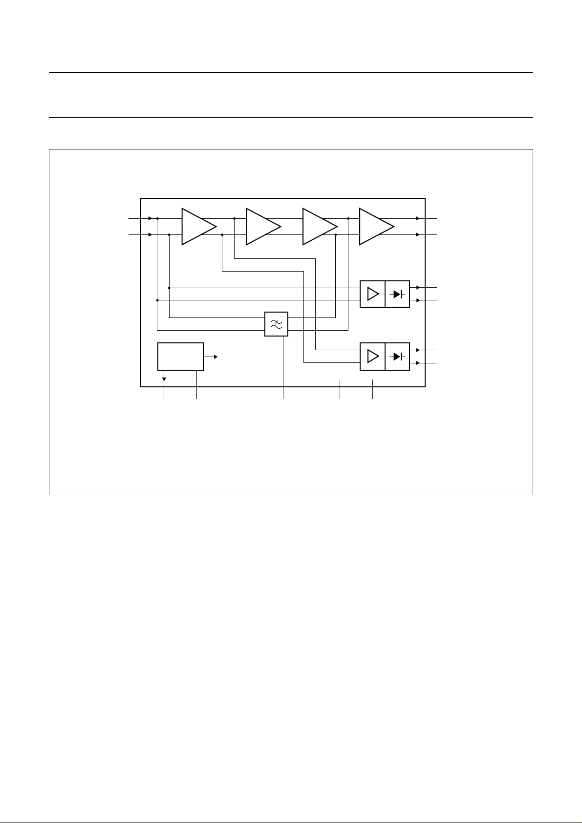
BLOCK DIAGRAM
handbook, full pagewidth
INQ
A
B
MGE745
32
OUT
30
OUTQ
3
AGC
43
AGCDC
19
LOS
18
LOSDC
8
IN
6
AMP A AMP B AMP C AMP D
22
reference
voltage
for all cells
45 44
COFF COFFQ GND
BAND GAP
21
REF
CAPA
V
EE
Fig.1 Block diagram.
1997 Nov 26 3
Philips Semiconductors Preliminary specification
SDH/SONET main amplifier OQ2538HP
PINNING
SYMBOL PIN DESCRIPTION TYPE
V
EE
1 negative power supply S
n.c. 2 not connected −
AGC 3 rectifier A output O
GND 4 ground S
GND 5 ground S
INQ 6 main amplifier inverting input I
GND 7 ground S
IN 8 main amplifier input I
GND 9 ground S
GND 10 ground S
n.c. 11 not connected −
V
EE
V
EE
12 negative power supply S
13 negative power supply S
n.c. 14 not connected −
n.c. 15 not connected −
GND 16 ground S
GND 17 ground S
LOSDC 18 rectifier B reference output O
LOS 19 rectifier B output O
GND 20 ground S
REF 21 band gap reference O
CAPA 22 pin for connecting band gap reference decoupling capacitor A
n.c. 23 not connected −
V
EE
V
EE
24 negative power supply S
25 negative power supply S
n.c. 26 not connected −
n.c. 27 not connected −
GND 28 ground S
GND 29 ground S
OUTQ 30 main amplifier inverted output O
GND 31 ground S
OUT 32 main amplifier output O
GND 33 ground S
GND 34 ground S
n.c. 35 not connected −
V
EE
V
EE
36 negative power supply S
37 negative power supply S
n.c. 38 not connected −
GND 39 ground S
n.c. 40 not connected −
(1)
1997 Nov 26 4
Philips Semiconductors Preliminary specification
SDH/SONET main amplifier OQ2538HP
SYMBOL PIN DESCRIPTION TYPE
GND 41 ground S
GND 42 ground S
AGCDC 43 rectifier A reference output O
COFFQ 44 pin for connecting automatic offset control capacitor (return) A
COFF 45 pin for connecting automatic offset control capacitor A
n.c. 46 not connected −
n.c. 47 not connected −
V
EE
48 negative power supply S
Note
1. Pin type abbreviations: O = Output, I = Input, S = power Supply, A = Analog function.
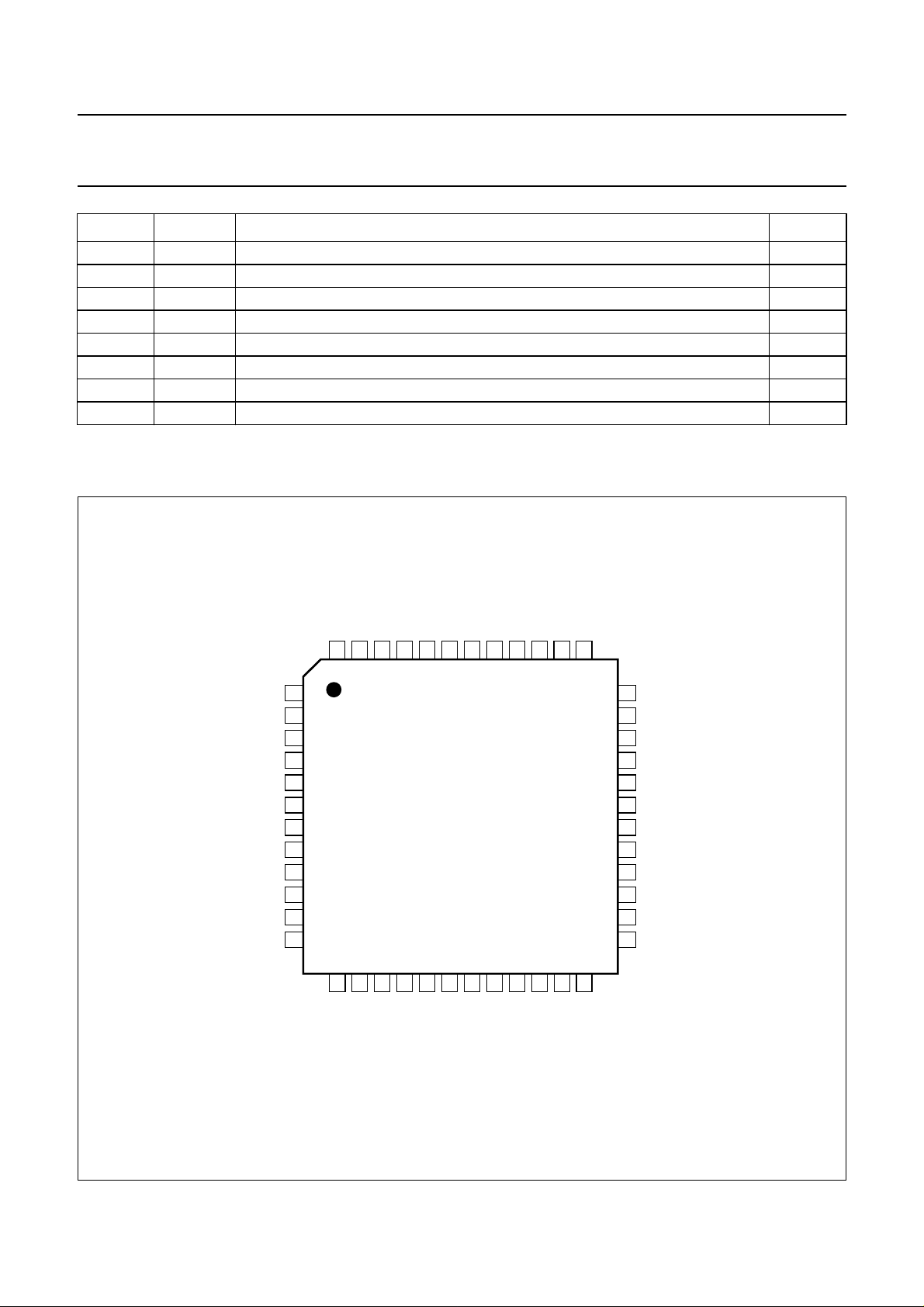
handbook, full pagewidth
EE
n.c.
n.c.
47
COFF
COFFQ
46
45
44
V
48
GND
AGCDC
43
42
GND
41
n.c.
40
GND
39
n.c.
38
EE
V
(1)
V
EE
n.c.
AGC
GND
GND
INQ
GND
GND
GND
n.c.
V
EE
V
1
2
3
4
5
6
7
IN
8
9
10
11
12
13
14
EE
n.c.
V
15
n.c.
OQ2538HP
16
17
GND
GND
18
19
LOS
LOSDC
20
GND
21
REF
22
CAPA
23
n.c.
36
EE
35
n.c.
34
GND
33
GND
32
OUT
31
GND
OUTQ
30
29
GND
GND
28
27
n.c.
26
n.c.
V
25
EE
24 37
MGE744
EE
V
Fig.2 Pin configuration.
1997 Nov 26 5
Philips Semiconductors Preliminary specification
SDH/SONET main amplifier OQ2538HP
FUNCTIONAL DESCRIPTION
The OQ2538HP is comprised of four DC-coupled amplifier
stages along with additional circuitry for offset
compensation and level detection.
The first amplifier stage contains a modified
Cherry/Hooper amplifying cell with high gain
(approximately 20 dB) and a wide bandwidth. Special
attention is paid to minimizing the equivalent input noise at
this stage, thus reducing the overall noise level. Additional
feedback is applied at the second and third stages,
improving isolation and reducing the gain to 14 dB per
stage. The last stage is an output buffer, a unity gain
amplifier, with an output impedance of 100 Ω.
The total gain of the OQ2538HP amounts to 48.5 dB, thus
providing a constant CML-compatible output signal over a
wide input signal range.
Two rectifier circuits are used to measure the input signal
level. Two separate RF pre-amplifiers are used to
generate the voltage gain needed to obtain a suitable
rectifier output voltage. For rectifier A the gain is
approximately 18 dB, for rectifier B it is about 14 dB.
The output of rectifier A can be used for AGC at the
pre-amplifier stage in front of the OQ2538HP. The output
of rectifier B can be used for LOS detection. There is a
linear relationship between the rectifier output voltage and
the input signal level provided the amplifiers are not
saturated.
Because the four gain stages are DC-coupled and provide
a high overall gain, the effect of the input offset can be
considerable. The OQ2538HP features an internal offset
compensation circuit for eliminating the input offset.
The bandwidth of the offset control loop is determined by
an external capacitor.
COFF and COFFQ offset compensation
where C
is the capacitance connected between COFF
ext
and COFFQ.
REF and CAPA band gap output and decoupling capacitance
To reduce band gap noise levels, a 1 nF decoupling
capacitor on CAPA is recommended. Since the band gap
is referenced to the negative supply, V
, the decoupling
EE
capacitor should be connected between CAPA and VEE.
The band gap voltage is present for test purposes only.
It is not intended to serve as an external reference.
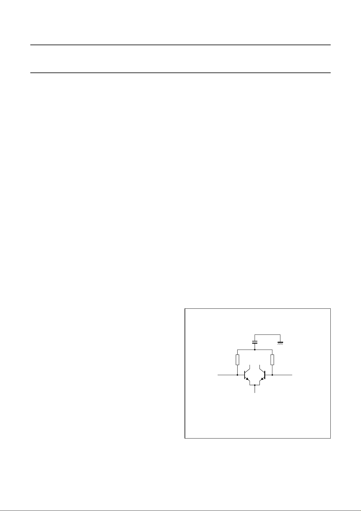
RF input and output connections
Striplines, or microstrips, with an odd mode characteristic
impedance of Z
=50Ω must be used for the
o,odd
differential RF connections on the PCB. This applies to
both the input signal pair IN and INQ and to the output
signal pair OUT and OUTQ. The two lines in each pair
should be the same length.
RF input matching circuit
The input circuit for pins IN and INQ contains internal
100 Ω resistors decoupled to ground via an internal
common mode 6 pF capacitor. The topology is depicted in
Fig.3. An external 200 Ω resistor between IN and INQ is
recommended in order to match the inputs to a differential
transmission line, coupled microstrip or stripline with an
odd mode impedance Z
andbook, halfpage
o,odd
of 50 Ω.
GND
6 pF
Automatic offset compensation eliminates the input offset
of the OQ2538HP. This offset cancellation influences the
low frequency gain of the amplifier stages. With a
capacitance of 100 nF between COFF and COFFQ the
loop bandwidth will be less than 1.5 kHz, small enough to
have no influence on amplifier gain over the frequencies of
interest. If the capacitor were omitted, the loop bandwidth
would be greater than 30 MHz, which would influence the
input signal gain. The loop bandwidth can be calculated
from the following formula:
=
------------------------------------------------
loop
2π 1250 Ω× C
1
×
ext
(1)f
1997 Nov 26 6
100 Ω
IN INQ
100 Ω
MGM114
Fig.3 RF input topology.
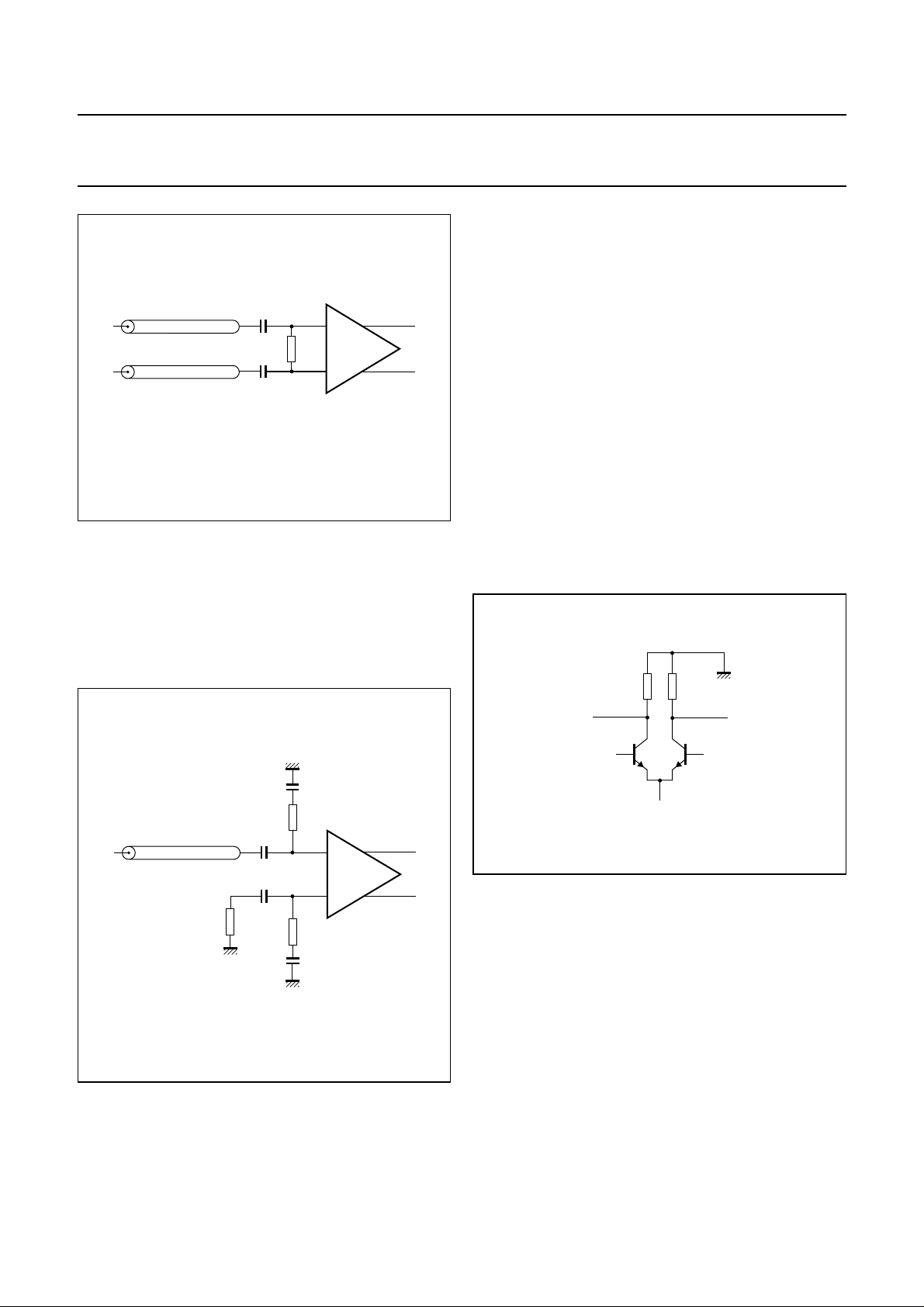
Philips Semiconductors Preliminary specification
SDH/SONET main amplifier OQ2538HP
In both cases, the essence of good matching is the equity
of the circuitry on both input pins. The impedance seen on
pins IN and INQ should be as equal as possible. For more
handbook, halfpage
differential line
Z
o(odd)
= 50 Ω
22 nF
200 Ω
22 nF
IN
INQ
MGM115
Fig.4 Differential input matching.
For single-ended excitation, separate matching networks
on IN and INQ, as depicted in Fig.5, achieve optimum
matching. Care should be taken to avoid DC loading, since
the OQ2538HP controls its own DC input voltage.
The resistors on the unused input, INQ, may be combined
for convenience.
information see
the OM5801 STM16 demo board.
RF output matching circuit
Matching of the main amplifier outputs, OUT and OUTQ, is
not mandatory. In most applications, the receiving end of
the transmission line will be properly matched, so very little
reflection will occur. Matching the transmitting end to
absorb these reflections is only recommended for very
sensitive applications. In such cases, 100 Ω pull-up
resistors should be connected from OUT and OUTQ to
ground, as close as possible to the IC pins. These
matching resistors will not be needed in most applications,
however. The output circuit of the OQ2538HP is depicted
in Fig.6. For more information see
AN96051
handbook, halfpage
“Application Note AN96051
” describing
“Application Note
” describing the OM5801 STM16 demo board.
GND
handbook, halfpage
transmission line
Fig.5 single-ended input matching.
Zo = 50 Ω
50 Ω
22 nF
22 nF
22 nF
100 Ω
100 Ω
22 nF
IN
INQ
MGM116
100 Ω 100 Ω
OUT
OUTQ
MGM117
Fig.6 RF output topology.
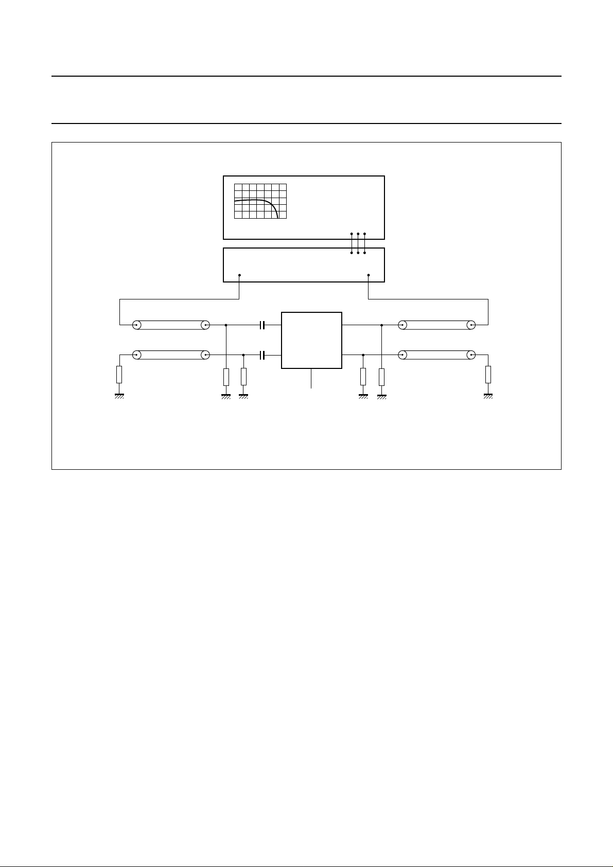
RF gain and group delay measurements
The measurement set-up shown in Fig.7 was used to
measure the single-ended small signal gain as specified in
Chapter “Characteristics”. Since the network analyzer can
only perform single-ended measurements, the
single-ended matching scheme described above is used
to match the inputs of the OQ2538HP to 50 Ω. For greater
accuracy, the outputs are also matched. The gain
measured with this set-up is denoted by S21. Graphs of
typical S21 and group delay characteristics are shown in
Figs 8 and 9. The OQ2538HP test PCB used for these
measurements can be supplied on request.
1997 Nov 26 7
Philips Semiconductors Preliminary specification
SDH/SONET main amplifier OQ2538HP
handbook, full pagewidth
6 GHz NETWORK ANALYZER
S-PARAMETER TEST SET
P = −50 dBm
PORT 1 PORT 2
Zo = 50 Ω
50 Ω semi rigid
100 pF
OQ2538HP
test PCB
IN
OUT
Zo = 50 Ω
50 Ω semi rigid
100 pF
INQ
100 Ω
50 Ω SMA
termination
50 Ω semi rigid
100 Ω
Fig.7 S21 and group delay measurement set-up.
Although the differential voltage gain of the OQ2538HP
cannot be measured directly, it can be calculated from S21.
The differential voltage gain is 6 dB greater than the
measured S21 value, typically 46 dB (40 dB + 6 dB). If the
100 Ω matching resistors on the output are omitted, the
differential voltage gain is increased by a further 2.4 dB,
typically to 48.4 dB. This is due to the fact that the output
load is increased from 25 to 33 Ω, so the output voltage is
increased by a factor of 1.32 (2.4 dB).
V
EE
OUTQ
= −4.5 V
100 Ω 100 Ω
50 Ω semi rigid
50 Ω SMA
termination
MGM111
1997 Nov 26 8
 Loading...