

查询OM6208供应商
INTEGRATED CIRCUITS
DATA SH EET
OM6208
65 x 96 pixels matrix grey-scale
LCD driver
Product specification
Supersedes data of 2003 Jan 30
2003 feb 10

Philips Semiconductors Product specification
65 x 96 pixels matrix grey-scale LCD driver OM6208
CONTENTS
1 FEATURES
2 APPLICATIONS
3 GENERAL DESCRIPTION
4 ORDERING INFORMATION
5 BLOCK DIAGRAM
6 PINNING
7 FUNCTIONAL DESCRIPTION
7.1 I/O buffers and interfaces
7.2 Oscillator
7.3 Address counter
7.4 Display data RAM
7.5 Display address counter
7.6 Timing generator
7.7 Data processing
7.8 High voltage generator
7.9 Bias voltage generator
7.10 Command decoder
7.11 Orthogonal function generator
7.12 Reset
7.13 Row drivers and column drivers
8 RAM ADDRESSING
8.1 Display data RAM structure
8.1.1 Horizontal/vertical addressing
8.1.2 Mirror Y
8.1.3 Mirror X
9 SERIAL INTERFACING
9.1 Serial peripheral interface
9.1.1 Write mode
9.1.2 Read mode
9.2 Serial interface (3-line)
9.2.1 Write mode
9.2.2 Read mode
9.2.3 Read data format
10 I2C-BUS INTERFACE
10.1 Characteristics of the I2C-bus (Hs-mode)
10.1.1 System configuration
10.1.2 Bit transfer
10.1.3 Start and stop conditions
10.1.4 Acknowledge
10.2 I2C-bus Hs-mode protocol
10.3 Command decoder
10.4 Read mode
11 INSTRUCTIONS
11.1 Description of command bits
11.2 Frame frequency setting and oscillator tuning
11.3 Initialization
11.4 Reset function
11.5 Power-down mode
11.6 Display Control
11.6.1 Horizontal mirroring
11.6.2 Vertical mirroring
11.7 Set Y address of RAM
11.8 Set X address of RAM
11.9 Bias levels
11.10 LCD drive voltage
11.10.1 LCD drive voltage generation
11.10.2 Temperature measurement
11.10.3 Temperature compensation
11.11 Grey-scale mode and black-and-white mode
11.12 N-line inversion and frame inversion
12 LIMITING VALUES
13 HANDLING
14 DC CHARACTERISTICS
15 AC CHARACTERISTICS
16 APPLICATION INFORMATION
16.1 Protection from light
16.2 Chip-on-glass displays
16.3 Application examples
17 MODULE MAKER PROGRAMMING
17.1 V
17.2 Factory defaults
17.2.1 Configuration derived from OTP cells
17.2.2 Defaults from interface registers
17.3 Seal bit
17.4 OTP architecture
17.4.1 OTP operational effects
17.5 Interface commands
17.5.1 CALMM instruction
17.5.2 Refresh instruction
17.6 Example of filling the shift register
17.7 Programming flow
17.8 Programming specification
18 DEVICE PROTECTION DIAGRAM
19 BONDING PAD INFORMATION
20 TRAY INFORMATION
21 DATA SHEET STATUS
22 DEFINITIONS
23 DISCLAIMERS
24 PURCHASE OF PHILIPS I2C COMPONENTS
calibration
LCD
2003 feb 10 2

Philips Semiconductors Product specification
65 x 96 pixels matrix grey-scale LCD driver OM6208
1 FEATURES
• Single chip LCD Multiple Row Addressing (MRA)
grey-scale/colour controller/driver
• Four grey levels/colours
• 65 row outputs and 96 column outputs
• Display Data RAM (DDRAM) 65 × 96 × 2 bits
• Selectable interface:
– 6.5 MHz 3-line or 4-line Serial Peripheral
Interface (SPI)
– 6.5 MHz 3-line serial interface
– High speed I2C-bus interface.
• On-chip:
– Configurable voltage multiplier generating V
external V
– Four-segment V
also possible
LCD
LCD
temperature compensation
LCD
;
– Generation of intermediate LCD bias voltage
– Oscillator requires noexternal components; external
clock input also possible
– Integrated charge pump capacitors (reducing total
system cost).
• External reset input
• Temperature read-back
• Selectable N-line inversion and frame inversion
• CMOS compatible inputs
• Logic supply voltage range 1.7 to 3.3 V
• High-voltage generator supply voltage range
2.4 to 4.5 V
• Display supply voltage range 5 to 9 V
• Low power consumption; suitable for battery operated
systems
• Programmable row pad mirroring for compatibility with
Tape Carrier Packages (TCP) and with Chip-On
Glass (COG) applications
• Status read which allows chip recognition
• Start address line; for example, for scrolling the
displayed image
• Slim chip layout; suitable for COG, COF and TCP
applications
• Operating temperature range −40 to +85 °C.
2 APPLICATIONS
• Telecom equipment
• Portable instruments
• Point of sale terminals.
3 GENERAL DESCRIPTION
The OM6208 is a low power CMOS LCD controller driver,
designed to drive a graphic display of 65 rows and
96 columns. All necessary functions for the display are
provided in a single chip, including on-chip generation of
LCD supply and bias voltages, resulting in a minimum of
external components and low power consumption. The
OM6208 can be interfaced to microcontrollers via a serial
bus and I2C-bus.
The OM6208 is manufactured in n-well CMOS technology.
Operation is with the substrate at VSS potential.
4 ORDERING INFORMATION
PACKAGE
TYPE NUMBER
NAME DESCRIPTION VERSION
OM6208MU/2DA/1 − chip with bumps in tray −
2003 feb 10 3
Philips Semiconductors Product specification
65 x 96 pixels matrix grey-scale LCD driver OM6208
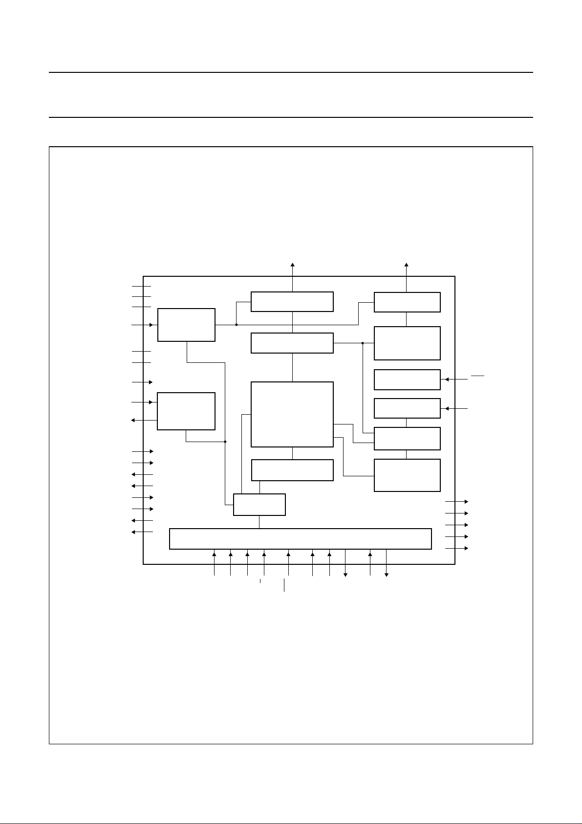
5 BLOCK DIAGRAM
handbook, full pagewidth
V
LCDIN
V
OTPPROG
V
LCDSENSE
V
LCDOUT
V
V
V
V
V
DD1
DD2
DD3
SS1
SS2
T1
T2
T3
T4
T5
T6
T7
T8
BIAS
VOLTAGE
GENERATOR
HIGH
VOLTAGE
GENERATOR
C0 to C95
COLUMN DRIVERS
DATA PROCESSING
DISPLAY DATA RAM
(DDRAM)
[65 × 96] × 2
ADDRESS COUNTER
COMMAND
DECODER
I/O BUFFERS and INTERFACES
OM6208
R0 to R64
ROW DRIVERS
ORTHOGONAL
FUNCTION
GENERATOR
RESET
OSCILLATOR
TIMING
GENERATOR
DISPLAY
ADDRESS
COUNTER
RES
OSC
V
2H
V
1H
V
C
V
1L
V
2L
ID3/SA0; ID4/SA1
]
1:0
[
PS
D/C
MX
Fig.1 Block diagram.
2003 feb 10 4
SCLH/SCE
SCLK
SDATA
SDO
MGW821
SDAH
SDAHOUT
Philips Semiconductors Product specification
65 x 96 pixels matrix grey-scale LCD driver OM6208
6 PINNING
SYMBOL PAD
V
LCDIN
V
LCDOUT
V
LCDSENSE
V
DD2
V
DD3
(1)
DESCRIPTION
5 to 8 LCD supply voltage input; note 2
9 to 15 LCD supply voltage output from high voltage generator; note 2
16 regulation input to high voltage generator; note 2
17 to 26 supply voltage 2; note 3
27 to 29 supply voltage 3; note 3
OSC 30 oscillator input; note 4
D/
C 31 data/command input/output; note 5
PS[1:0] 32 and 33 interface selection inputs
V
DD1
SDAHOUT 44 I
34 to 39 supply voltage 1; note 3
2
C-bus data output; note 6
SCLK 46 serial data clock input; used in 3-line or 4-line SPI or 3-line serial interface
mode
SDAH 52 I2C-bus data input; note 7
SDO 53 serial data output; note 8
SDATA 54 serial data input; note 9
V
SS2
V
SS1
55 to 61 ground 2 (analog ground); note 10
62 to 67 ground 1 (digital ground); note 10
MX 68 horizontal mirroring input
T3 69 test outputs; note 11
T4 70
T1 71
T2 72
T5 73
T6 74
2
ID3/SA0; ID4/SA1 75 and 76 manufacturer device identification/I
V
DD1
SCE 83 I2C-bus clock input/serial chip enable input in 3-line or 4-line SPI mode; note 5
SCLH/
V
OTPPROG
77 supply voltage 1 (tie-off pad)
84 to 86 supply voltage input for OTP programming; note 13
C-bus slave address input pads; note 12
RES 88 external reset input; active low; must be applied to initialize the chip properly
R32 to R64 105 to 137 LCD row driver outputs
V
C
138 bias buffer output; note 14
T8 141 test outputs; note 11
T7 142
V
1L
143 bias buffer output; note 14
C95 to C48 144 to 191 LCD column driver outputs
C47 to C0 194 to 241
R31 to R0 247 to 278 LCD row driver outputs
V
1H
V
2L
V
2H
244 bias buffer outputs; note 14
245
246
2003 feb 10 5

Philips Semiconductors Product specification
65 x 96 pixels matrix grey-scale LCD driver OM6208
Notes
1. Dummy pads are located at positions 1, 2, 4, 40 to 43, 45, 47 to 51, 78 to 82, 87, 89 to 92, 95 to 104, 139, 140, 192,
193, 242, 243, 279 and 280; alignment marks are located at positions 3 and 93; an alignment bump is located at
position 94.
2. Positive power supply for the liquid crystal display (see also Figs 38, 39 and 40):
a) If the internal voltage generator is used, pads V
LCDIN,VLCDSENSE
b) An external LCD supply voltage can be incorporated using the V
then switched off, pad V
connected to the V
LCDIN
LCDOUT
input; V
must be open-circuit (not connected to pad V
should be applied according to the specified voltage range. In Power-down
DD2,3
mode, the external LCD supply voltage must be switched off.
3. V
DD2
and V
supply the internal voltage generator, both have the same voltage and may be connected together
DD3
outside of the chip; V
supplies the remainder of the chip. V
DD1
then care must be taken with respect to the supply voltage range.
4. When the on-chip oscillator is used, the OSC input must be connected to V
then this is connected to the OSC input. If both the oscillator and external clock are inhibited by connecting pad OSC
to V
, the display is not clocked and may be in a DC state. To avoid this, the chip should always be put into
SS1
Power-down mode before stopping the clock.
5. This input is not used with the 3-line serial interface and must be connected to V
use.
6. SDAHOUT is the serial data acknowledge output from the I2C-bus interface. By connecting SDAHOUT to SDAH
externally, the SDAH line becomes fully I2C-bus compatible. Having the acknowledge output separated from the
serial data line is advantageous in COG applications because here the track resistance from the SDAHOUT pad to
the system SDAH line can be significant and a potential divider can be generated by the bus pull-up resistor and the
ITO track resistance. It is possible that during the acknowledge cycle the OM6208 will not be able to create a valid
logic 0. By splitting the SDAH input from the SDAHOUT output the device could be used in a mode that ignores the
acknowledgebit.ThereforeinCOGapplicationswheretheacknowledgecycleis required, it is necessary to minimize
the track resistance from the SDAHOUT pad to the system SDAH line to guarantee a valid logic 0. When SDAHOUT
is not used, it must be connected to V
7. When I2C-bus is not used, this pad must be connected to V
DD1
or V
SS1
.
DD1
8. SDO is a push-pull output; when it is intended to use the readback function of the OM6208, this pad must be
connected to the SDATA pad, or used separately; when I2C-bus interface is selected, this pad should be connected
to V
DD1
or V
SS1
.
9. When I2C-bus interface is selected this pin should be connected to V
10. Supply rails V
SS1
and V
must be connected together.
SS2
11. Test padsT1 to T8arenotaccessibletousers:T1, T2, T5 and T6 must be connected to VSS; T3,T4,T7and T8 must
be open-circuit.
12. Module identification bits: these bits may be read back via the ‘read back’ instruction; when the I2C-bus interface is
being used, these bits are the two LSBs of the slave address.
13. V
OTPROG
configuration, then V
can be connected to SCLH/SCE pad to reduce the external connections. If not connected in this
OTPROG
should be open-circuit during normal operation.
14. These pads are not accessible to users and must be left open-circuit; an explanation of the bias buffer function is
given in Section 11.9.
DD1
or V
, V
and V
pad; the internal voltage generator must
LCDIN
and V
DD2
.
SS1
or V
DD1
must be connected together.
LCDOUT
) and pad V
LCDIN
can be connected together but
DD3
. If an external clock signal is used,
DD1
or V
SS1
DD1
.
SS1
LCDSENSE
when this interface is in
2003 feb 10 6
Philips Semiconductors Product specification
65 x 96 pixels matrix grey-scale LCD driver OM6208
7 FUNCTIONAL DESCRIPTION
7.1 I/O buffers and interfaces
One of four industrial standard interfaces can be selected
using the interface configuration inputs PS1 and PS0.
2
Table 1 Serial/I
C-bus interface selection
PS1 PS0 SELECTED INTERFACE
0 0 3-line SPI
0 1 4-line SPI
10I
2
C-bus interface
1 1 3-line serial interface
7.2 Oscillator
The on-chip oscillator provides the clock signal for the
display system. No external components are required
when the internal oscillator is used. An external clock
signal, if used, is connected to this input.
7.3 Address counter
The Address Counter (AC) assigns addresses to the
displaydataRAMforwriting. The X address X[6:0] and the
Y address Y[4:0] are set separately.
7.6 Timing generator
The timing generator produces the various signals
required to drive the internal circuitry. Internal chip
operation is not affected by operations on the data bus.
7.7 Data processing
The data processing block receives data from the RAM
and the orthogonal function from the logic circuits, then
selects the correct voltage level to be provided to the
columns.
7.8 High voltage generator
The high voltage generator provides the programmed
V
to the bias voltage generator block.
LCD
7.9 Bias voltage generator
Thebiasvoltagegeneratorgeneratesallthevoltagelevels
required for the MRA driving system.
7.10 Command decoder
The command decoder identifies command words arriving
at the interface and routes the data bytes that follow to
their destination.
7.4 Display data RAM
The OM6208 contains a 65 × 96 × 2 bit static RAM which
stores the display data. The display data RAM is divided
into 17 banks of 96 bytes, although only two bits of the
17th bank are used. During RAM access, data is
transferred to the RAM via the serial interface. There is a
direct correspondence between X address and column
output number.
7.5 Display address counter
The display is generated by simultaneously reading out
the RAM content for two or four rows, depending on the
current display size that is selected. This content will be
processed with the corresponding set of two or four
orthogonal functions and so generate the signals for
switchingthepixelsofthedisplayonoroff according to the
RAM content.
The display status (all dots on/all dots off and
normal/inverse video) is set by the bits DON, DAL and E
in the command Display control (see Table 8).
7.11 Orthogonal function generator
The orthogonal function generator generates a set of
orthogonal functions suitable for the selected value of p
(number of active rows).
7.12 Reset
The reset block handles the hardware reset input (RES)
andsoftware reset and provides all internal blocks with the
required reset signal.
7.13 Row drivers and column drivers
The OM6208 contains 65 row and 96 column drivers
which connect the appropriate LCD bias voltages in
sequence to the display in accordance with the data to be
displayed. A typical MRA driving scheme with waveforms
for p = 4 is shown in Fig.2. The value of p represents the
number of simultaneously selected rows.
2003 feb 10 7
Philips Semiconductors Product specification
65 x 96 pixels matrix grey-scale LCD driver OM6208
handbook, full pagewidth
F1(t)
F2(t)
F3(t)
F4(t)
G1(t)
F1(t)
V
col(max)
V
C
V
col(min)
G1(t)
G1(t) = C [+ F1(t) − F2(t) − F3(t) + F4(t)
G1(t)
G2(t) G3(t)
G2(t) G3(t)
]
F2(t)
F3(t)
F4(t)
V
col(max)
G1(t)
V
C
V
col(min)
Fig.2 Typical MRA LCD driver waveforms for p = 4.
2003 feb 10 8
G1(t) = C [− F1(t) − F2(t) − F3(t) + F4(t)
MGW822
]
Philips Semiconductors Product specification
65 x 96 pixels matrix grey-scale LCD driver OM6208
8 RAM ADDRESSING
Data is downloaded in bytes into the RAM matrix of the
OM6208 as indicated in Fig.3. The display RAM has a
matrix of 65 × 96 × 2 bits. The columns are addressed by
the address pointer. The address ranges (decimal values)
handbook, full pagewidth
DOR = 1
LSB
MSB
DB0
DB1
DB2
DB3
DB4
DB5
DB6
DB7
P0
MSB
P0
LSB
P1
MSB
P1
LSB
P2
MSB
P2
LSB
P3
MSB
P3
LSB
P0
P1
P2
P3
P0
bank 0
P1
P2
P3
bank 1
bank 2
bank 3
.
DOR = 0
LSB
MSB
DB0
DB1
DB2
DB3
DB4
DB5
DB6
DB7
P3
LSB
P3
MSB
P2
LSB
P2
MSB
P1
LSB
P1
MSB
P0
LSB
P0
MSB
.
.
bank 13
bank 14
bank 15
X
X
X
bank 16
X
X
X
areX=0to95andY=0to16.TheYaddressrepresents
the bank number. Addresses outside these ranges are not
allowed.
The Data Order Bit (DOR) defines the bit order (LSB on
top or MSB on top) for writing into the RAM.
LSB
MSB
top of LCD
R0
R4
R8
R12
.
.
.
.
.
LCD
R16
R52
R56
R60
R64
Fig.3 DDRAM-to-display mapping.
2003 feb 10 9
MGW823
Philips Semiconductors Product specification
65 x 96 pixels matrix grey-scale LCD driver OM6208
8.1 Display data RAM structure
The mode for storing data in the display data RAM is
dependent on:
• Horizontal/vertical addressing mode set by bit V in the
‘RAM addressing mode’ instruction
• Data order set by bit DOR in the ‘data order’ instruction
• Mirror the X-axis set by input MX.
8.1.1 HORIZONTAL/VERTICAL ADDRESSING
Two different addressing modes are possible; horizontal
addressing mode and vertical addressing mode.
handbook, full pagewidth
01
192 193
288 289
384
2
98
194
290
386385
In the horizontal addressing mode (V = 0) the X address
increments after each byte. After the last X address
(X = 95), X wraps around to 0 and Y increments to
address the next row (see Fig.4).
In the vertical addressing mode (V = 1), the Y address
increments after each byte. After the last Y address
(Y = 16), Y wraps around to 0 and X increments to
address the next column (see Fig.5).
After the very last address, the address pointers wrap
around to address X = 0 and Y = 0 in both horizontal and
vertical addressing modes.
95
19196 97
0
Y address
handbook, full pagewidth
1440
1441 1442
1536
1537
0 95X address
1535
161631
MGW824
Fig.4 Sequence of writing data bytes into RAM with horizontal addressing (V = 0).
017
118
219
320
421
522
16 33
0 95X address
0
Y address
161631
MGW825
Fig.5 Sequence of writing data bytes into the RAM with vertical addressing (V = 1).
2003 feb 10 10

Philips Semiconductors Product specification
65 x 96 pixels matrix grey-scale LCD driver OM6208
8.1.2 MIRROR Y
The Mirror Y (MY) bit allows vertical mirroring:
• When MY = 1, the Y address space is mirrored; the
address Y = 0 is then located at the bottom of the
display (see Fig.6)
handbook, full pagewidth
0 95X address
• When MY = 0, the mirroring is disabled and the address
Y = 0 is located at top of the display (see Fig.7).
Refer also to Section 11.6.
16
0
Y address
MGW826
handbook, full pagewidth
Fig.6 RAM format addressing (MY = 1).
0 95X address
Y address
Fig.7 RAM format addressing (MY = 0).
0
16
MGW827
2003 feb 10 11
Philips Semiconductors Product specification
65 x 96 pixels matrix grey-scale LCD driver OM6208
8.1.3 MIRROR X
The Mirror X (MX) input allows a horizontal mirroring:
• When MX = 1, the X address space is mirrored; the
address X = 0 is then located at the right side (X
max
the display (see Fig.8)
handbook, full pagewidth
95 0X address
) of
Y address
• When MX = 0, the mirroring is disabled and the address
X = 0 is located at the left side (column 0) of the display
(see Fig.9).
Refer also to Section 11.6.
0
16
MGW828
handbook, full pagewidth
Fig.8 RAM format addressing (MX = 1).
0 95X address
Y address
Fig.9 RAM format addressing (MX = 0).
0
16
MGW829
2003 feb 10 12
Philips Semiconductors Product specification
65 x 96 pixels matrix grey-scale LCD driver OM6208
9 SERIAL INTERFACING
Communication with the microcontroller can occur via a
clock-synchronized serial peripheral interface. It is
possible to select two different 3-line (SPI and serial
interface) or a 4-line SPI interface. Selection is done via
the PS[1:0] inputs.
9.1 Serial peripheral interface
The Serial Peripheral Interface (SPI) is a 3-line or 4-line
interface for communication between the microcontroller
and the LCD driver chip. Three lines are common to both
3-line and 4-line SPI, these are SCE (chip enable), SCLK
(serial clock) and SDATA (serial data). For the 4-line SPI a
separate D/C line is added. The OM6208 is connected to
the serial data I/O of the microcontroller by pads SDATA
(data input) and SDO (data output) connected together.
handbook, full pagewidth
SCE
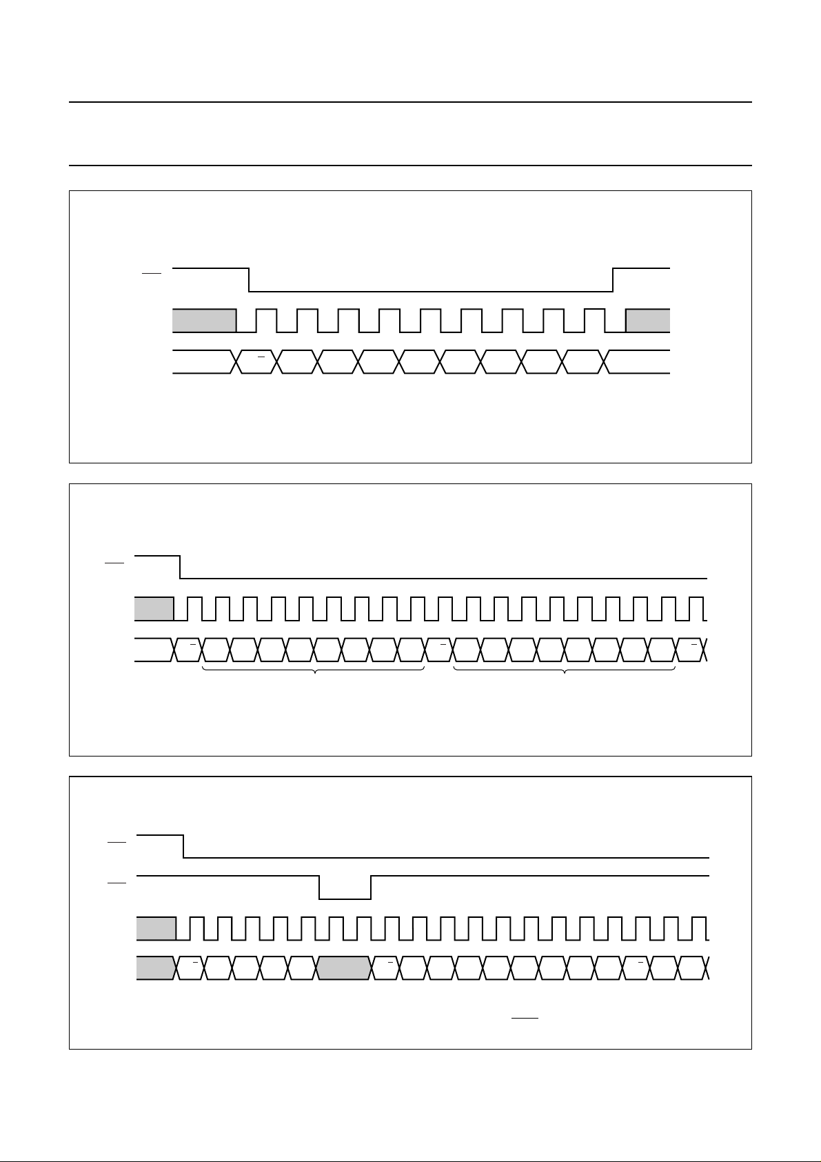
9.1.1 WRITE MODE
The display data/command indication may be controlled
by software or by the D/C select pin. When the D/C pad is
used, display data is transmitted when D/C is HIGH, and
command data is transmitted when D/C is LOW (see
Figs 10 and 11). When D/C is not used, the ‘display data
length’instructionis used toindicatethata specific number
of display data bytes (1 to 255) are to be transmitted (see
Fig.11). The next byte after the display data string is
handled as an instruction command.
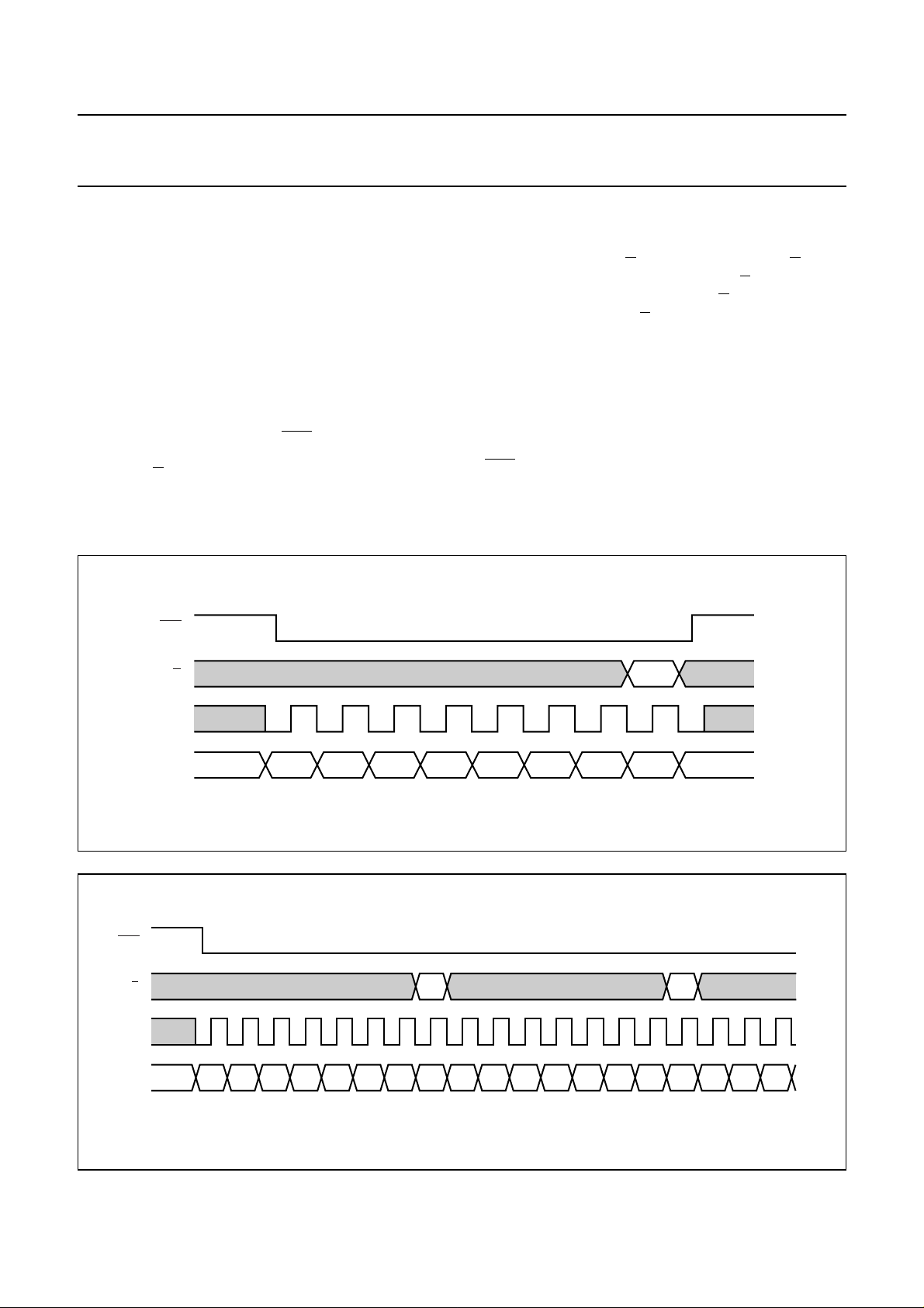
When the 3-line SPI interface is used the display
data/command is controlled by software (see Fig.12).
If SCE is pulled high during a serial display data stream,
the interrupted byte is invalid data but all previously
transmitted data is valid. The next byte received will be
handled as an instruction command (see Fig.13).
D/C
SCLK
SDATA
DB7 DB6 DB5 DB4 DB3 DB2 DB1 DB0
Fig.10 4-line SPI bus protocol; transmission of one byte.
handbook, full pagewidth
SCE
D/C
SCLK
SDATA DB7 DB6 DB5 DB4 DB3 DB2 DB1 DB0 DB7DB7 DB6 DB5 DB4 DB3 DB2 DB1 DB0
MGW744
DB6 DB5
MGW745
Fig.11 4-line SPI bus protocol; transmission of several bytes.
2003 feb 10 13
Philips Semiconductors Product specification
65 x 96 pixels matrix grey-scale LCD driver OM6208
handbook, full pagewidth
SCE
SCLK
SDATA DB7 DB6 DB5 DB4
handbook, full pagewidth
SCE
SCLK
SDATA
datadata data data data data
display data string
Fig.13 3-line SPI bus protocol: transmission interrupted by SCE.
DB2 DB1 DB0 DB2
display length instruction
and length data (two bytes)
data data
last
DB7 DB6 DB5 DB4 DB3 DB1 DB0
data
Fig.12 3-line SPI bus protocol; transmission of several bytes.
instruction
instructiondisplay data string
DB7DB7 DB6 DB5 DB4 DB3 DB2 DB1 DB0 DB6 DB5 DB4
MGW746
MGW747
2003 feb 10 14
Philips Semiconductors Product specification
65 x 96 pixels matrix grey-scale LCD driver OM6208
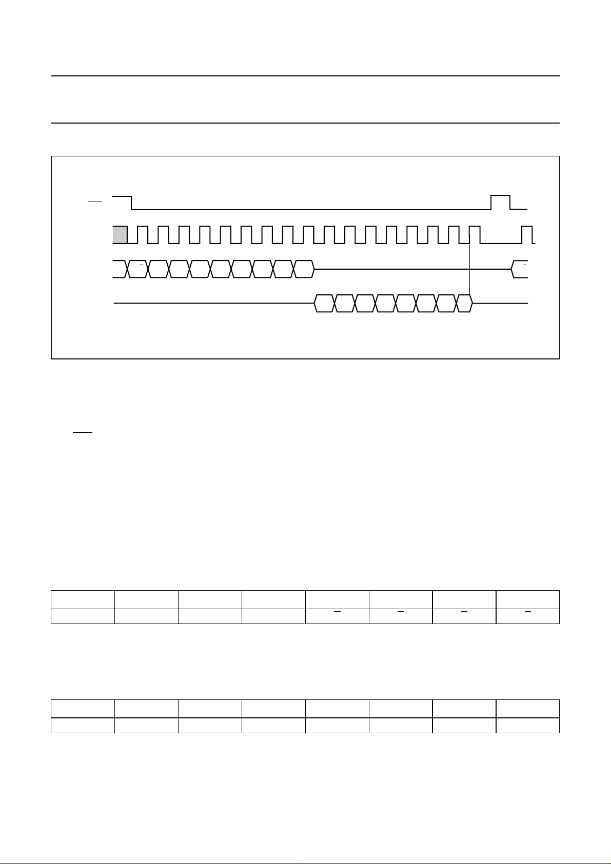
9.1.2 READ MODE
The read mode of the interface means that the
microcontroller reads data from the OM6208. To do so the
microcontroller first has to send a command, the read
status command, and then OM6208 will respond by
transmitting data on the SDO line. After that, SCE is
required to go HIGH (see Fig.14).
The OM6208 samples the SDATA data at rising SCLK
edges, but shifts SDO data at falling SCLK edges. Thus
handbook, full pagewidth
SCE
RES
SCLK
SDATA DB7 DB6 DB5 DB4 DB2DB3 DB1 DB0
the SDO data is available to be read by the microcontroller
at rising SCLK edges.
After the read status command has been sent, the SDATA
line must be set to 3-state (high-impedance) not later than
at the falling SCLK edge of the last bit (see Fig.14).
For the read data format, see Section 9.2.3; the serial
interface timing diagram is given in Chapter 15.
SDO
instruction
read out data
Fig.14 Read mode SPI 3- and 4-line interfaces.
DB2DB7 DB6 DB5 DB4 DB3 DB1 DB0
MGU629
2003 feb 10 15
Philips Semiconductors Product specification
65 x 96 pixels matrix grey-scale LCD driver OM6208
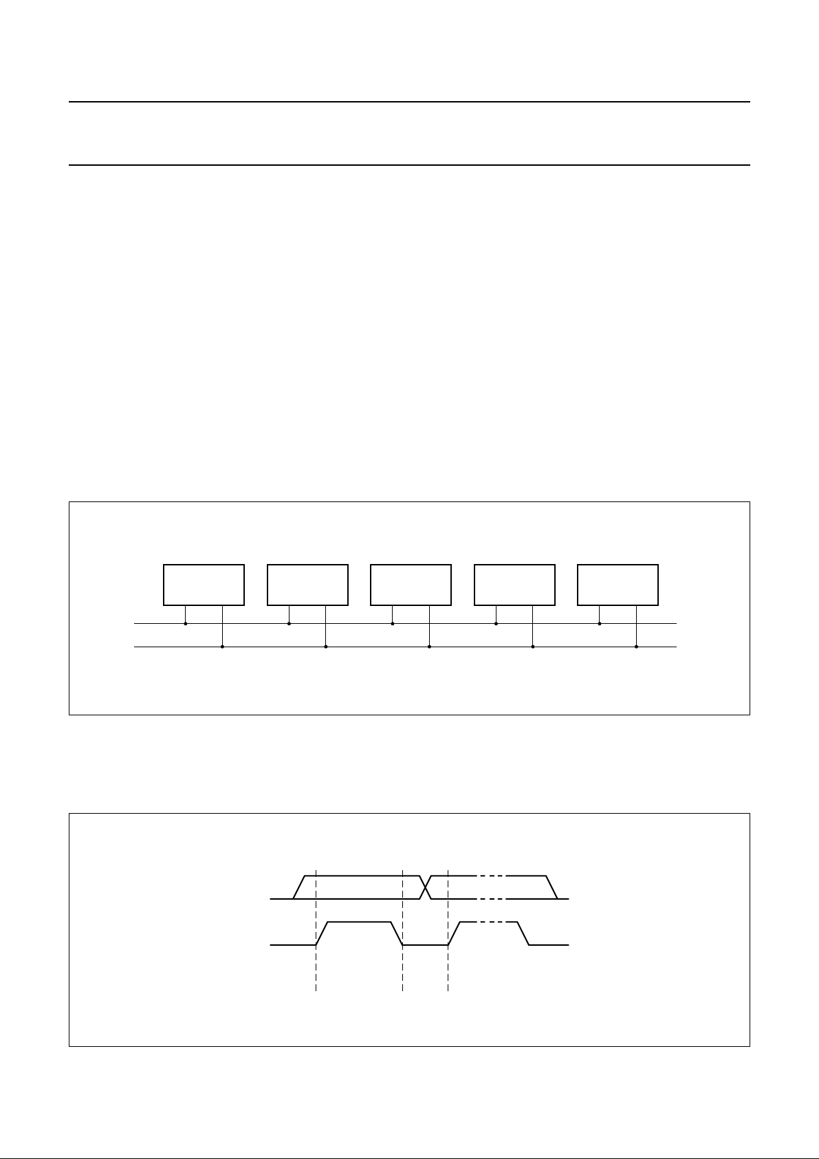
9.2 Serial interface (3-line)
The serial interface is also a 3-line bidirectional interface
for communication between the microcontroller and the
LCD driver chip. The three lines are SCE (chip enable),
SCLK(serialclock) and SDATA (serialdata).TheOM6208
is connected to the SDA of the microcontroller by the
SDATA(datainput)andSDO (data output) pads which are
connected together.
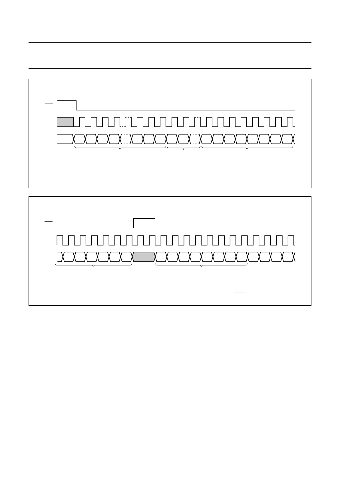
9.2.1 WRITE MODE
The write mode of the interface means that the
microcontroller writes instructions and data to the
OM6208. Each data packet contains a control bit D/C and
a transmission byte. If D/C is LOW, the following byte is
interpreted as command byte. The instruction set is given
in Table 7. If D/C is HIGH, the following byte is stored in
the display data RAM. After every data byte the address
counter is incremented automatically. The general format
of the write mode and the definition of the transmission
byte is shown in Fig.15.
Any instruction can be sent in any order to the OM6208.
The MSB is transmitted first. The serial interface is
initialized when SCE is HIGH. In this state, SCLK clock
pulses have no effect and no power is consumed by the
serial interface. A falling edge on SCE enables the serial
interface and indicates the start of data transmission.
Figures 16, 17 and 18 show the protocol of the write
mode:
• When SCE is HIGH, SCLK clocks are ignored. During
the HIGH time of SCE the serial interface is initialized
(see Fig.16)
• At the falling SCE edge, SCLK must be LOW
(see Fig.32)
• SDATA is sampled at the rising edge of SCLK
• D/C indicates whether the byte is a command (D/C=0)
or RAM data (D/C = 1) byte; it is sampled with the first
rising SCLK edge
• If SCE stays LOW after the last bit of a command/data
byte, the serial interface is ready for the D/C bit of the
next byte at the next rising edge of SCLK (see Fig.17)
• A reset pulse with RES interrupts the transmission. The
data being written into the RAM may be corrupted. The
registers are cleared. If SCE is LOW after the rising
edge of RES, the serial interface is ready to receive the
D/C bit of a command/data byte (see Fig.18).
D/C
(1)
transmission byte
handbook, full pagewidth
D7 D6 D5 D4 D3 D2 D1 D0
D/C
MSB LSB
D/C
(1) A transmission byte may be a command byte or a data byte.
transmission byte
transmission byte
Fig.15 Serial data stream, write mode.
2003 feb 10 16
D/C
transmission byte
MGW713
Philips Semiconductors Product specification
65 x 96 pixels matrix grey-scale LCD driver OM6208
handbook, full pagewidth
SCE
SCLK
SDATA
D/C
DB7 DB6 DB5 DB4 DB3 DB2 DB1 DB0
Fig.16 Write mode: a control bit followed by a transmission byte.
handbook, full pagewidth
SCE
SCLK
SDATA DB7D/C DB6 DB5 DB4 DB3 DB2
DB1 DB0
MGU630
DB7D/C DB6 DB5 DB4 DB3 DB2 DB1 DB0 D/C
transmission byte
transmission byte
Fig.17 Write mode: transmission of several bytes.
handbook, full pagewidth
SCE
RES
SCLK
SDATA DB7D/C DB6 DB5 DB4 DB7DB7 DB6 DB5 DB4 DB3 DB2 DB1 DB0
Fig.18 Write mode: interrupted by reset (RES).
2003 feb 10 17
MGU631
DB6D/C D/C
MGU632
Philips Semiconductors Product specification
65 x 96 pixels matrix grey-scale LCD driver OM6208
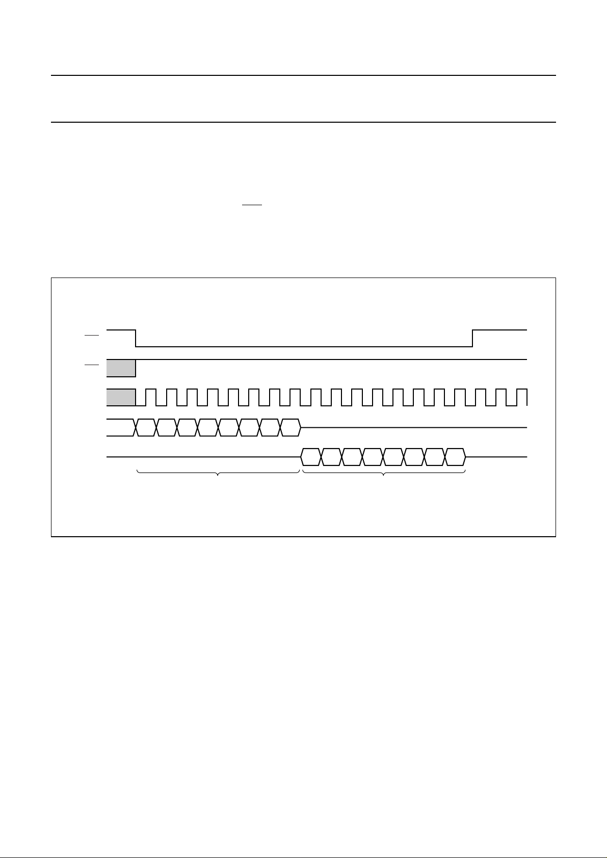
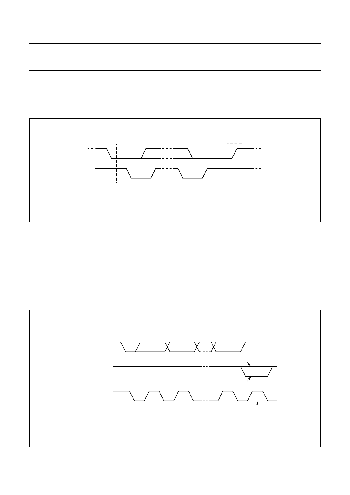
9.2.2 READ MODE
handbook, full pagewidth
SCE
SCLK
SDATA
SDO
DB7D/C DB6 DB5 DB4
DB3 DB2 DB1 DB0
Fig.19 Read mode serial interface 3-line.
The read mode of the interface means that the
microcontroller reads data from the OM6208. To do so the
microcontroller first has to send a command, the read
statuscommand,and then the followingbyteistransmitted
in the opposite direction using SDO (see Fig.19). After
that, SCE is required to go HIGH before a new command
is sent.
The OM6208 samples the SDATA data at rising SCLK
edges and shifts SDO data at falling SCLK edges. Thus
the SDO data is available for the microcontroller to read at
rising SCLK edges.
After the read status command has been sent, the SDATA
linemustbe set to 3-state not later then at the falling SCLK
edge of the last bit (see Fig.19).
D/C
DB7 DB6 DB5 DB4 DB3 DB2 DB1
DB0
MCE176
The 8th read bit is shorter than the others because it is
terminated by the rising SCLK edge (see Fig.35). The last
rising SCLK edge sets SDO to 3-state after the delay
time t4.
9.2.3 READ DATA FORMAT
Regardless of which serial interface is used there are five
bits that can be read (ID1 to ID4 and VM) and one
temperatureregister.For the bits, one bit istransmittedper
byte read and is selected by issuing the appropriate read
instruction from the instruction set. Bits ID1 and ID2 are
hard-wired so that ID1 always returns a logic 0 and ID2
always returns a logic 1. Bits ID3 and ID4 are the
identification bits and are set via ID3/SA0 and ID4/SA1
pads. The format for the read bit, B, is shown in Table 2.
Table 2 Read data format
D7 (MSB) D6 D5 D4 D3 D2 D1 D0 (LSB)
(1)
x
BBBBBBB
Note
1. x = undefined.
Table 3 Read temperature sensor
Sending the instruction to read back the temperature sensor data will select the following status byte.
D7 (MSB) D6 D5 D4 D3 D2 D1 D0 (LSB)
(1)
x
TD[6] TD[5] TD[4] TD[3] TD[2] TD[1] TD[0]
Note
1. x = undefined.
2003 feb 10 18
Philips Semiconductors Product specification
65 x 96 pixels matrix grey-scale LCD driver OM6208
10 I2C-BUS INTERFACE
2
10.1 Characteristics of the I
C-bus (Hs-mode)
The I2C-bus Hs-mode is for bidirectional, two-line
communication between different ICs or modules with
speeds up to 3.4 MHz. The only difference between
Hs-modeslavedevicesandF/S-modeslavedevicesisthe
speed at which they operate, therefore the buffers on the
SDAH output have an open drain. This is the same for
2
C-bus master devices which have an open-drain SDAH
I
output and a combination of an open-drain pull-down and
current source pull-up circuits on the SCLH output. Only
the current source of one master is enabled at any one
time and only during Hs-mode. Both lines must be
connected to a positive supply via a pull-up resistor.
Data transfer may be initiated only when the bus is not
busy.
SDA
SCL
MASTER
TRANSMITTER/
RECEIVER
SLAVE
RECEIVER
TRANSMITTER/
RECEIVER
10.1.1 S
YSTEM CONFIGURATION
Definition (see Fig.20):
• Transmitter: the device that sends the data to the bus
• Receiver: the device that receives the data from the bus
• Master: the device that initiates a transfer, generates
clock signals and terminates a transfer
• Slave: the device addressed by a master
• Multi-master: more than one master can attempt to
control the bus at the same time without corrupting the
message
• Arbitration: procedure to ensure that, if more than one
master simultaneously tries to control the bus, only one
is allowed to do so and the message is not corrupted
• Synchronisation: procedure to synchronize the clock
signals of two or more devices.
SLAVE
MASTER
TRANSMITTER
MASTER
TRANSMITTER/
RECEIVER
MGA807
Fig.20 System configuration.
10.1.2 BIT TRANSFER
One data bit is transferred during each clock pulse (see
Fig.21). The data on the SDAH line must remain stable
handbook, full pagewidth
SDA
SCL
data line
stable;
data valid
Fig.21 Bit transfer.
2003 feb 10 19
during the HIGH period of the clock pulse as changes in
the data line at this time will be interpreted as a control
signal.
change
of data
allowed
MBC621
Philips Semiconductors Product specification
65 x 96 pixels matrix grey-scale LCD driver OM6208
10.1.3 START AND STOP CONDITIONS
BothdataandclocklinesremainHIGHwhenthe bus is not
busy (see Fig.22). A HIGH-to-LOW transition of the data
handbook, full pagewidth
SDA
SCL
S
START condition
Fig.22 Definition of START and STOP conditions.
10.1.4 ACKNOWLEDGE
Each byte of 8 bits is followed by an acknowledge bit (see
Fig.23). The acknowledge bit is a HIGH signal put on the
bus by the transmitter during which time the master
generates an extra acknowledge related clock pulse.
A slave receiver which is addressed must generate an
acknowledge after the reception of each byte. Also a
master receiver must generate an acknowledge after the
reception of each byte that has been clocked out of the
line, while the clock is HIGH is defined as the START
condition (S). A LOW-to-HIGH transition of the data line
while the clock is HIGH is defined as the STOP
condition (P).
SDA
P
STOP condition
SCL
MBC622
slave transmitter. The device that acknowledges must
pull-down the SDA line during the acknowledge clock
pulse, so that the SDA line is stable LOW during the HIGH
period of the acknowledge related clock pulse (set-up and
hold times must be taken into consideration). A master
receiver must signal an end of data to the transmitter by
not generating an acknowledge on the last byte that has
been clocked out of the slave. In this event the transmitter
must leave the data line HIGH to enable the master to
generate a stop condition.
handbook, full pagewidth
DATA OUTPUT
BY TRANSMITTER
DATA OUTPUT
BY RECEIVER
SCL FROM
MASTER
S
START
condition
Fig.23 Acknowledge on the I2C-bus.
2003 feb 10 20
not acknowledge
acknowledge
acknowledgement
9821
clock pulse for
MBC602
Philips Semiconductors Product specification
65 x 96 pixels matrix grey-scale LCD driver OM6208
R/
10.2 I2C-bus Hs-mode protocol
TheOM6208 is a slave receiver/transmitter. If data is to be
read from the device the SDAHOUT and SDAH pads must
be connected for acknowledge to be used (see Table 1,
note 6).
Hs-mode can only commence after the following
conditions.
• START condition (S)
• 8-bit master code (00001XXX)
• not-acknowledge bit (A).
The master code has two functions as shown in Figs 24
and 25, it allows arbitration and synchronization between
competing masters at F/S-mode speeds, resulting in one
winner.Also the master code indicates the beginning of an
Hs-mode transfer.
As no device is allowed to acknowledge the master code,
then a master code transmission must be followed by a
not-acknowledge (A). After this A bit, and the SCLH line
has been pulled up to a HIGH level, the active master
switches to Hs-mode and enables at tHthe current-source
pull-up circuit for the SCLH signal (see Fig.25).
The active master will then send a repeated START
condition (Sr) followed by a 7-bit slave address with a
W bit, and receives an acknowledge bit (A) from the
selected slave. After each acknowledge bit (A) or
not-acknowledge bit (A) the active master disables its
current-source pull-up circuit. The active master
re-enables its current source again when all devices have
released and the SCLH signal reaches a HIGH level. The
rising of the SCLH is done by a resistor pull-up and so is
slower, the last part of the SCLH rise time is speeded up
because the current source is enabled. Data transfer only
switches back to F/S-mode after a STOP (P) condition.
The write sequence that occurs after the Hs-mode is
selected is shown in Fig.26. The sequence is initiated with
a START (S) condition from the I2C-bus master which is
followed by the slave address. All slaves with the
corresponding address acknowledge in parallel, all the
others will ignore the I2C-bus transfer.
After an acknowledgement cycle of a write (W), one or
morecommandwordsfollowwhichdefinethestatusofthe
addressed slaves. A command word consists of a control
byte, which defines Co and D/C, plus a data byte (see
Fig.26 and Table 4).
The last control byte is tagged with a cleared most
significantbit,the continuation bit Co. Thecontrolanddata
bytes are also acknowledged by all addressed slaves on
the bus.
Table 4 Co and Sr definition
Co D/C R/W ACTION
0 −−
1 −−
− 0
− 1
Afterthelast control byte, dependingontheD/C bit setting,
a series of display data bytes or command data bytes may
follow. If the Sr bit was set to logic 1, these display bytes
are stored in the display RAM at the address specified by
the data pointer. The data pointer is automatically updated
and the data is directed to the intended OM6208 device.
If the Sr bit of the last control byte was set to logic 0, these
command bytes will be decoded and the setting of the
device will be changed according to the received
commands. The acknowledgement after each byte is
made only by the addressed OM6208. At the end of the
last control byte to be sent; only a stream of data bytes are allowed to follow; this stream
may only be terminated by a STOP or repeated START condition
another control byte will follow the data byte unless a STOP or repeated START condition
is received
0 data byte will be decoded and used to set up the device
1 data byte will return the status byte
0 data byte will be stored in the display RAM
1 RAM read back is not supported
transmission the I2C-bus master issues a STOP
condition (P) and switches back to F/S-mode, however, to
reduce the overhead of the master code, it i s possible that
a master links a number of Hs-mode transfers, separated
by repeated START conditions (Sr).
A read sequence (see Fig.27) follows after the Hs-mode is
selected. The OM6208 will immediately start to output the
requested data until a not acknowledge is transmitted by
the master. The write access should be terminated by a
repeated START condition so that the Hs-mode is not
disabled.
2003 feb 10 21

Philips Semiconductors Product specification
65 x 96 pixels matrix grey-scale LCD driver OM6208
handbook, full pagewidth
handbook, full pagewidth
SDAH
SCLH
F/S-mode
S R/WMASTER CODE Sr SLAVE ADD.
Hs-mode (current-source for SCLH enabled)
Fig.24 Data transfer format in Hs-mode.
S
1 2 to 5
8-bit Master code 00001xxx
F/S-mode
AA A/ADATA
(n bytes + ack.)
6789
P
Hs-mode continues
SLAVE ADD.
Sr
MSC616
t
1
A
t
H
F/S mode
Sr
SDAH
SCLH
t
H
= MCS current source pull-up
= Rp resistor pull-up
7-bit SLA
16789 67891
2 to 5
R/W A
Hs-mode
Fig.25 Complete data transfer in Hs-mode.
2003 feb 10 22
n × (8-bit DATA + A/A)
2 to 5
Sr P
If P then
F/S mode
If Sr (dotted lines)
then Hs-mode
t
FS
MSC618

Philips Semiconductors Product specification
65 x 96 pixels matrix grey-scale LCD driver OM6208
handbook, full pagewidth
Sr01111
slave address
handbook, full pagewidth
acknowledge
from OM6208
S
S
0A
A
A
0
1
R/W
1
D/C
from OM6208
control byte
acknowledge
A data byte data byte
2n ≥ 0 bytes
acknowledge
from OM6208
control byte
0A AP
A
D/C
CoCo
1 byte
Fig.26 Master transmits in Hs-mode to slave receiver; write mode.
NOT acknowledgement
from Master
P
STOP condition
MGW831
Sr01111
slave address
acknowledgement
from OM6208
S
S
A
1
A
0
(1)
status information A
1A
R/W
acknowledge
from OM6208
MSB . . . . . . . . . . . LSB
acknowledge
from OM6208
n ≥ 0 bytes
MGW830
(1) These bits are set by inputs ID3/SA0 and ID4/SA1.
Fig.27 Master receives from slave transmitter (status register is read); read mode.
10.3 Command decoder
The command decoder identifies command words that
arrive on the I2C-bus:
• Pairs of bytes
– firstbytedetermineswhether information is display or
instruction data
– 2nd byte contains information.
• Stream of information bytes after Co = 0; display or
instruction data depending on last D/C.
2003 feb 10 23
Themost-significantbitofa control byte is the continuation
bit Co. If this bit is logic 1, it indicates that only one byte,
either command or RAM-data, will follow. If this bit is
logic 0, it indicates that a series of bytes, either command
or RAM-data, may follow. The DB6 bit of a control byte is
the RAM-data/command bit D/C. When this bit is logic 1, it
indicates that a RAM-data byte will be transferred next.
If the bit is logic 0, it indicates that a command byte will be
transferred next.

Philips Semiconductors Product specification
65 x 96 pixels matrix grey-scale LCD driver OM6208
10.4 Read mode
I2C-bus read mode operates differently from the other
interfaces. Two different status bytes can be read back
and are selected by first sending a ‘read’ instruction.
Sending the instruction to read ID1, ID2 and VM will select
the status byte shown in Table 5.
Sending the instruction to read back the temperature
sensor will select the status byte shown in Table 6.
A repeated START or STOP and START must then be
generated followed by the slave address with the R/W bit
set to read in order to read the status register.
Table 5 Read status byte ID1, ID2 and VM
D7 (MSB) D6 D5 D4 D3 D2 D1 D0 (LSB)
(1)
x
(1)
x
(1)
x
(1)
x
(1)
x
VM ID2
(2)
ID1
Notes
1. x = undefined.
2
2. Bits ID3 and ID4 are not available for I
C-bus because they are used to make up the two LSBs of the slave address.
Table 6 Read temperature sensor
D7 (MSB) D6 D5 D4 D3 D2 D1 D0 (LSB)
(1)
x
TD[6] TD[5] TD[4] TD[3] TD[2] TD[1] TD[0]
Note
1. x = undefined.
(2)
2003 feb 10 24

Philips Semiconductors Product specification
65 x 96 pixels matrix grey-scale LCD driver OM6208
11 INSTRUCTIONS
The OM6208 may be interfaced via 3-line or 4-line Serial
PeripheralInterface (SPI), 3-line serialinterfaceor I2C-bus
interface. In all cases, processing of instructions is
asynchronous and does not require the internal/external
oscillator to be running.
Data transmission to OM6208 may be of two types, those
that define the operating mode of the device (commands)
and those that fill display RAM (data). Table 7 lists all
commands that are recognised by OM6208.
The Most Significant Bit (MSB) is sent first. The mode in
which the D/C bit is defined varies with the type of serial
D/C bit definitions:
• With 4-line SPI interface selected, the D/C bit is
implemented as hard-wired input at pad D/C
• With 3-line SPI interface selected, the D/C bit is not
implemented and all transmission are commands by
default unless preceded by the Display data length
command
• With3-lineserial and I2C-businterfaceselected, the D/C
bit is implemented through the interface protocol.
Commands can consist of one byte (single-byte) and two
bytes (double-byte). Unless otherwise specified,
commands may be executed in any order.
interface that is used.
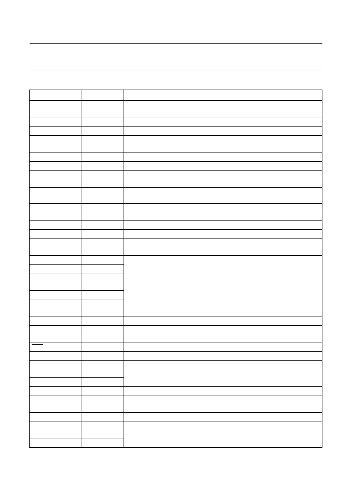
Table 7 Instruction set
Instructions not expressly defined in this table and reserved instructions must not be used.
COMMAND BYTE
COMMAND NAME D/
C
(MSB) D6 D5 D4 D3 D2 D1
D
D
D
D
D
Write data 1 D
Horizontal addressing 0 0 0 0 0 X
Horizontal addressing 0 0 0 0 1 δ
7
6
5
4
3
3
(1)
Power control 0 0 0101PCδ
D
2
1
X
X
X
2
1
X
6
5
(1)
(LSB)
FUNCTION DESCRIPTION
D0
D
RAM data
0
X0set X address; lower 4 bits
X4set X address; upper 3 bits
(1)
δ
charge pump on/off
Charge pump control 0 0 011110 1set multiplication factor
(1)
0 δ
Set V
Set V
PR
PR
00 0100V
01 00V
Set bias 0 0 0110BS
(1)
(1)
(1)
(1)
δ
δ
δ
δ
pr4Vpr3Vpr2Vpr1
(1)
δ
pr7Vpr6
2BS1
S
1
S
0
V
write Vpr register
pr5
V
write Vpr register
pr0
BS0set bias
Display mode 0 1 010010DALall on/normal display
Display mode 0 1 010011 Enormal/inverse display
Display mode 0 1 010111DONdisplay ON/OFF
Data order 0 1 010100DORswap RAM MSB/LSB order
RAM addressing 0 1 010101 Vvertical or horizontal mode
Vertical addressing 0 1 0 1 1 Y
Vertical addressing 0 0 011111Y
Vertical mirroring 0 1 1 0 0 MY δ
ID read 0 1 101101 0identification: ID1
ID read 0 1 101101 1identification: ID2
ID read 0 1 101110 0identification: ID3
ID read 0 1 101110 1identification: ID4
Y
3
(1)
Y
2
δ
Y0set Yaddress
1
4
(1)
(1)
δ
set Yaddress
mirror Y
(2)(3)
(2)(3)
(2)
(2)
Temperature sense 0 1 101111 0temperature read back
VM read 0 1 101111 1voltage monitor
(3)(4)
Row control 0 1 110000BRSswap the bottom rows
2003 feb 10 25

Philips Semiconductors Product specification
65 x 96 pixels matrix grey-scale LCD driver OM6208
COMMAND BYTE
COMMAND NAME D/C
(MSB) D6 D5 D4 D3 D2 D1
(LSB)
Software reset 0 1 110001 0internal reset
NOP 01 110001 1no operation
Display data length 0 1 110100 0display data length for 3-line
Temperature
compensation
Temperature
compensation
Frame frequency
range, oscillator tune
and mode
Temperature
0D
00 011100 0setTCslopes A and B (SLA
(1)
0 δ
00 011100 1setTC slopes C and D
(1)
0 δ
00 011110 0frame frequency range and
0 MOD T
01 110101TCEenable/disable temperature
D
7
6
D
5
SLB2SLB1SLB0δ
SLD2SLD1SLD0δ
T
2
1
D
4
T
0
D
D
3
2
(1)
SLA2SLA1SLA
(1)
SLC2SLC1SLC
(1)
δ
FR2FR1FR
D
1
compensation enable
Oscillator selection 0 0 011101ECexternal oscillator
OTP programming 0 1 11100OSECALMMenter calibration mode and
LOAD0 01 101100 0write0 to shift register
LOAD1 01 101100 1write1 to shift register
Select factory
01 110110SFDenable/disable defaults
defaults
N-line inversion and
super-frame inversion
01 010110 1N-line inversion and
0FINL
6NL5
00 1δ
01 01000δ
NL4NL3NL2NL
(1)
(1)
δ
(1)
δ
NL
1
(1)
δ
(1)
δ
(1)
01 010110 0reserved
(1)
01 1010δ
(1)
δ
01 110100 1reserved
01 11001δ
(1)
01 110111δ
(1)
(1)
(1)
δ
01 11101δ
01 1111δ
FUNCTION DESCRIPTION
D0
SPI
D
0
and SLB)
0
(SLC and SLD)
0
oscillator tune and working
0
mode
compensation
control programming
super-frame Inversion
0
(1)
δ
reserved
(1)
δ
reserved
(1)
δ
reserved
(1)
δ
reserved
(1)
reserved
(1)
δ
reserved for testing
(1)
δ
reserved for testing
Notes
1. δ = don’t care.
2. ID1, ID2, ID3, ID4 and VM are read back via interface as described in Section 9.2.3. Reading back with I2C-bus
interface is possible for temperature, ID1, ID2 and VM, as described in Section 10.4.
3. ID1 will always return to logic 0; ID2 will always return to logic 1. The VM bit is set to logic 1 when the charge pump
is running and logic 0 when the charge pump is not running.
4. If the Factory Defaults bit (MMFD) has been programmed to 1, then the SFD instruction is ignored and the device
will always use the OTP default data.
2003 feb 10 26

Philips Semiconductors Product specification
65 x 96 pixels matrix grey-scale LCD driver OM6208
11.1 Description of command bits
Table 8 Bit descriptions
BIT 0 1 RESET STATE
DON display off display on 0
E normal display inverse video mode 0
DAL normal display all pixel on 1
MY no Y mirroring Y mirroring 0
PC charge pump off charge pump on 0
DOR normal data order MSB/LSB transposed for RAM data 0
V horizontal addressing vertical addressing 0
BRS bottom rows are not mirrored bottom rows are mirrored 0
EC internal oscillator is selected external clock to be used 0
(2)
(1)
(1)
0
0
0
(2)
(2)
(2)
(2)
(2)
(2)
(2)(3)
(2)(3)
(2)
(2)
(2)
CALMM exit OTP calibration mode enter OTP calibration mode
TCE disable temperature compensation enable temperature compensation 1
OSE disable OTP programmed voltage enable OTP programmed voltage
SFD use interface programmed data use OTP programmed data
MOD grey-scale mode is selected black-and-white mode is selected 0
SLA[2:0] select slope for segment A 000
SLB[2:0] select slope for segment B 000
SLC[2:0] select slope for segment C 000
SLD[2:0] select slope for segment D 000
X[6:0] sets X address (column) for writing in the RAM 0000000
Y[4:0] sets Yaddress (bank) for writing in the RAM 00000
S[1:0] charge pump multiplication factor (see Table 10) 0000
NL[6:0] sets N-line inversion (see Table 18) 0001101
FR[2:0] sets frame frequency range (see Table 11) 001
T[2:0] oscillator tune; sets frame frequency within a range (see Table 11) 110
D[7:0] display data length for 3-line SPI interface 00000000
VPR[7:0] V
register 00000000
PR
BS[2:0] bias setting level (see Table 13) 000
FI super-frame inversion 0
Notes
1. Calibration mode may not be entered if the SEAL bit has been set. Programming is only possible when in calibration
mode.
2. Thesevaluescanbe set by the module maker. If the factory defaults OTP bit (MMFD) has been set then these values
cannot be changed via the interface. Otherwise, the OTP data will only be used if bit SFD is set to 1.
3. FR[2:0] = 001 and T[2:0] = 110 gives 150 Hz as default frame frequency.
2003 feb 10 27

Philips Semiconductors Product specification
65 x 96 pixels matrix grey-scale LCD driver OM6208
Table 9 Display and power mode bits DON, DAL and E
(1)
DON DAL
00X
(2)
E
(3)
display off; all row and column
DESCRIPTION
outputs at VSS; oscillator on;
HV generator enabled
(3)
01X
Power-downmode;displayoff;
all row and column outputs at
VSS; oscillator off;
HV generator disabled
1 0 0 normal display mode
1 0 1 inverse display mode
11X
(3)
all pixels on
Notes
1. The DAL bit has priority over the
E bit.
2. Refer also to Table 17.
3. X = don’t care.
Table 10 Multiplication settings for charge pump
S1 S0
VOLTAGE
MULTIPLIER
004×
015×
106×
117×
Table 11 Frame frequencies for f
FR2 FR1 FR0
DIVISION
RATIO
= 400 kHz
osc
f
frame
(Hz)
0 0 0 2448 163.4
0 0 1 3265 122.5
0 1 0 4082 98.0
0 1 1 4896 81.7
1 0 0 5714 70.0
1 0 1 7340 54.5
1 1 0 8968 44.6
1 1 1 11428 35.0
Oscillator tuning is controlled by the parameter T[2:0]. As
a result of oscillator tuning, f
is increased by
OSC
approximately 4% per step according to the equation
f
OSC
400 kHz 1 0.04 T×+()×=
(1)
where T is the decimal value of T[2:0].
Example. For the default values given in Table 8
(i.e. FR[2:0] = 001 and T[2:0] = 110) the selected frame
frequency is 122.5 Hz × (1 + 6 × 0.04) = 151.9 Hz.
Equation (1) shows the typical value of the oscillator
frequency. The accuracy of this parameter is defined in
Chapter 15. The frame frequency accuracy results directly
from the oscillator accuracy.
11.2 Frame frequency setting and oscillator tuning
Grey-scale mode and black-and-white mode require
different frame frequencies. The appropriate frame
frequency (f
(f
) using a presettable divider as shown in the equation
osc
) is derived from the oscillator frequency
frame
f
f
=
frame
OSC
--------------------------------division ratio
There are eight possible divider settings and these are
selected by the parameter FR[2:0], see Table 11.
2003 feb 10 28
11.3 Initialization
Immediately following power-on, all internal registers and
the RAM content are undefined. A reset pulse must be
applied to the
RES pad.
Reset is accomplished by applying an external reset pulse
(active LOW) to the RES input. When reset occurs within
the specified time, all internal registers are reset, however
the RAM remains undefined. The state after reset is
described in Section 11.4.
At power-on, the RES input must be ≤0.3V
reachesV
after V
DD1
pulse can be applied when V
(orhigher)within the maximum timet
DD(min)
going HIGH (see Fig.37). Alternatively a reset
is stable.
DD1
DD1
when V
DD1
VHRL
A reset can also be made by sending a reset command.
This command can be used during normal operation but
not to initialize the chip after power-on.
After power-off, the RES input must not be HIGH when
V
is not HIGH.
DD1

Philips Semiconductors Product specification
65 x 96 pixels matrix grey-scale LCD driver OM6208
11.4 Reset function
After reset, the LCD driver is in Power-down mode, the
RAM is undefined and the internal registers have the
status shown in Table 8.
11.5 Power-down mode
In the Power-down mode:
• All LCD outputs (row and column outputs) are at V
SS
(display off)
• Bias generator and V
external V
supply can be applied or disconnected
LCD
generator are switched off;
LCD
• Oscillator is off (an external clock is possible)
• RAM contents are unchanged; RAM data can be written
• V
is discharged to VSS.
LCD
Power-down mode is active when the display is off
(DON = 0) and all the pixels are on (DAL = 1).
11.6 Display Control
The bits DON, E and DAL select the display mode (see
Table 9).
11.6.1 HORIZONTAL MIRRORING
When the MX input is at logic 0, the display RAM is written
from left to right (X = 0 is on the left side).
11.7 Set Yaddress of RAM
Y[4:0] defines the Y address of the display RAM.
Table 12 Yaddress range
Y4 Y3 Y2 Y1 Y0 DISPLAY RAM
0 0 0 0 0 bank 0
0 0 0 0 1 bank 1
0 0 0 1 0 bank 2
0 0 0 1 1 bank 3
0 0 1 0 0 bank 4
0 0 1 0 1 bank 5
0 0 1 1 0 bank 6
0 0 1 1 1 bank 7
0 1 0 0 0 bank 8
0 1 0 0 1 bank 9
0 1 0 1 0 bank 10
0 1 0 1 1 bank 11
0 1 1 0 0 bank 12
0 1 1 0 1 bank 13
0 1 1 1 0 bank 14
0 1 1 1 1 bank 15
1 0 0 0 1 bank 16
When the MX input is set to 1, the display RAM is written
from right to left (X = 0 is on the right side).
The MX input value has an impact on the way the RAM is
written: if a horizontal mirroring of the display is desired,
the RAM must be rewritten after changing the MX pad
value.
11.6.2 VERTICAL MIRRORING
When the MY bit is set to logic 1, the display is mirrored
vertically.
Achangeofthisbithasanimmediateeffect on the display,
it is not necessary to rewrite RAM for the effect to take
place.
11.8 Set X address of RAM
The X address points to the columns. The range of X is
0 to 95.
11.9 Bias levels
TheOM6208is a grey-scale driver able toprovidedifferent
bias voltage levels for rows and columns. The row voltage
values are V
LCD,VSS
and VC, generated using the resistor
chain shown in Fig.28.
The five levels used to drive the columns are shown in
Fig.28. These are V2L, V1L,VC, V1H and V2H, all of which
depend on the value of alpha. Table 13 shows all possible
combinations of alpha settable by programming the
BS[2:0] bits.
2003 feb 10 29

Philips Semiconductors Product specification
65 x 96 pixels matrix grey-scale LCD driver OM6208
handbook, halfpage
F
α is in the range 0.0 to 1.05.
Table 13 Bias setting levels for p = 4
BS2 BS1 BS0 F/G α a
0 0 0 1.000 0.00 4.00
0 0 1 1.075 0.15 4.30
0 1 0 1.150 0.30 4.60
0 1 1 1.225 0.45 4.90
1 0 0 1.300 0.60 5.20
1 0 1 1.375 0.75 5.50
1 1 0 1.450 0.90 5.80
1 1 1 1.525 1.05 6.10
V
LCD
αR
V
2H
R
G
R
R
R
αR
V
1H
V
C
V
1L
V
2L
VSS = V
Fig.28 Bias system.
Because the voltage level of the row depends on the
programmed bias level, it can be seen that
The situation where F = G occurs only when BS[2:0] is
zero and alpha is zero. In this case αR = 0 and G = F;
therefore V
internal buffers are no longer needed and therefore are
switched off to reduce power consumption.
The relationship between F and G is defined by the
parameter a (indicated in Table 13) and p as follows
= V
row(max)
row(min)
MGW832
2H=VLCD
FG≥
and V2L=VSS, also two of the
F
a
=
----
-- -
G
p
Each of the eight possible values of alpha results in a
different set of five values for the column voltages.
Bias level F (see Fig.28) is half of the maximum row
voltage level as shown by the equation
V
LCD
F
=
------------ 2
Figure 28 also shows that G is used to define the
maximum column voltage level related to the V
C
level.
2003 feb 10 30
It can be seen from Fig.28 that
F
a
-- p
α 2+()
----------------- 2
---G
α
1
+== =
--2
or
a
α
--2
1+
p⋅= α
a
1–
-- -
p
2⋅=
The BS[2:0] bias bits can be selected by a command and
also can be programmed by OTP.

Philips Semiconductors Product specification
65 x 96 pixels matrix grey-scale LCD driver OM6208
The relationship between the parameters F, p, a and N
(number of rows of the display) and the V
V
voltage values according to the typical LCD
off(rms)
on(rms)
and
properties of the pixel are shown in equations (2) and (3).
pa2N2a++()⋅
V
on(rms)
V
off(rms)
F
------------------------------------------ -⋅=
--a
pa2N2a–+()⋅
F
------------------------------------------⋅=
--a
N
N
(2)
(3)
11.10 LCD drive voltage
11.10.1 LCD
V
may be supplied externally or generated internally by
LCD
DRIVE VOLTAGE GENERATION
the on-chip capacitive charge pump. OM6208 features
on-chip capacitors resulting in a minimum of external
components required for operation (see Chapter 16).
The‘power control’ instruction may be used to switch V
LCD
generation on or off. The charge pump control instruction
may be used to select the required voltage multiplication
factor. The ‘set VPR’ instruction is used for programming
the LCD drive voltage V
The generation of V
This shows all factors that effect V
LCD.
in OM6208 is illustrated in Fig.29.
LCD
generation,
LCD
including the 6 bits of MMVOPCAL (from OTP) and the
7 bits resulting from the temperature compensation
mechanism. Equations summarizing all factors are
V
VPRMMVOPCAL V
OP
++=
T
(4)
Table 14 Parameters of V
LCD
SYMBOL VALUE UNIT
b 0.03 V
a3V
CAUTION
As the programming range for the internally generated
V
allows values above the maximum allowed V
LCD
(9 V), the user has to ensure, while setting the V
LCD
PR
register and selecting the temperature compensation,
that under all conditions and including all tolerances
V
remains below 9.0 V.
LCD
Also, because the programming range for the internally
generated V
allowed V
allows values below the minimum
LCD
(5 V), the user has to ensure, while setting
LCD
the VPR register and selecting the temperature
compensation, that under all conditions and including all
tolerances V
remains above 5.0 V.
LCD
and
LCD
VOPb⋅ a+=
(5)
V
Where:
[7:0] is set in the instruction decoder and is the
V
PR
programmed VPRregister value as an unsigned number
MMVOPCAL[5:0] is the value of the offset stored in the
OTP cells in twos complement format
VT[7:0] in twos complement format comes from the
temperature compensation block (see Table 16)
a and b are fixed constant values (see Table 14).
2003 feb 10 31

Philips Semiconductors Product specification
65 x 96 pixels matrix grey-scale LCD driver OM6208
handbook, full pagewidth
TEMPERATURE
MEASUREMENT
Fig.29 V
measured temperature slopes
B C D
A
V
T
TD
7
−40
generation including the temperature compensation and OTP calibration.
LCD
0
TEMPERATURE COMPENSATION
+85
T (°C)
[
]
7:0
V
PR
V
8
T
]
8
8
V
OP
abMMVOPCAL[5:0
MGW833
V
LCD
handbook, full pagewidth
V
LCD
b
a
00 01 02
VPR[7:0] programming: 00 to FF (HEX).
Assuming MMVOPCAL = 0 and VT=0V.
03 04 05 06
Fig.30 V
. . . . . . FD FE FF
programming of OM6208 shown as plots of equations (4) and (5).
LCD
MGT847
V
OP
2003 feb 10 32

Philips Semiconductors Product specification
65 x 96 pixels matrix grey-scale LCD driver OM6208
11.10.2 TEMPERATURE MEASUREMENT
The temperature measurement is repeated every
10 seconds. The measured value is provided as a 7-bit
digital value TD[6:0] which can be read back via the
interface. The temperature can be determined from
TD[6:0] using the equation
T 1.875 TD× 40–()°C=
(6)
11.10.3 TEMPERATURE COMPENSATION
Due to the temperature dependency of the liquid crystal’s
viscosity,the LCD controlling voltage V
mayhave to be
LCD
adjusted at different temperatures to maintain optimal
contrast.
Internal temperature compensation may be enabled via
the ‘temperature compensation enable’ instruction. When
the internal temperature compensation is applied (TCE bit
is set to 1) then according to Equation (4) the V
LCD
depends also on VT (the temperature compensation
component defined in Table 16), otherwise VT is
considered to be 0 V.
After the reset, the V
is fixed because the VPR is a
LCD
register that is reset to zero. The MMVOPCAL is also set
to zero because this comes from the registers of OTP that
are not refreshed yet, also VTis evaluated after the reset
because the temperature measurement block supplies a
TD value that is the default value stored in the register
after the reset.
The four temperature coefficients MA, MB, MC and MD
correspond to four equally spaced temperature regions.
Each coefficient can be selected from a choice of eight
different slopes, or multiplication factors. Each one of
these coefficients may be independently selected by the
user via the ‘temperature compensation enable’
instruction. The default for each slope register can be
stored in OTP.
Table 15 Temperature coefficients
Slopes of V
are calculated from equations (4), (5), (6)
LCD
and Table 16.
SLA, SLB, SLC
and SLD
MA, MB, MC
and MD
SLOPE
(mV/K)
111 3.00 −48
110 2.00 −32
101 1.25 −20
100 1.00 −16
011 0.75 −12
010 0.50 −8
001 0.25 −4
000 0.00 0
Temperature compensation is implemented by adding an
offset V
to the VPR value (additionally to the OTP
T
calibration offset MMVOPCAL).
The final result for V
calculation is an 8-bit positive
LCD
number as shown in equations (4) and (5). Care must be
taken by the user to ensure that the ranges of VPR,
MMVOPCAL and VT do not cause clipping and hence
undesired results. The adder stages will not permit
overflow or underflow and will clamp results to either end
of the range.
The temperature read-out generates a 7-bit result,
TD[6:0]. For temperatures below −40 °C, the value of TD
is zero. For temperatures above 79 °C, the value of TD is
higher than 63, but for VT calibration the value TD = 63 is
used.
The offset value VTmay be calculated from Table 16. The
effect on V
can be calculated by multiplying the offset
LCD
value with the value of b (from Table 14).
For example, if T = −10 °C, TD = 16 and MB = 1.25 then
V
LCDoffset
=30mV×(32 − 16) × 1.25 = 600 mV.
Table 16 Temperature compensation equations
TEMPERATURE RANGE (°C) TD RANGE EQUATION
−40 to −11 0 to 15 V
−10 to +19 16 to 31 V
+20 to +49 32 to 47 V
+50 to +79 48 to 63 V
= (16 × MB) + MA × (16 − TD)
T
= (32 − TD) × MB
T
= −(TD − 32) × MC
T
= −(16 × MC)+MD×(TD − 48)
T
2003 feb 10 33

Philips Semiconductors Product specification
65 x 96 pixels matrix grey-scale LCD driver OM6208
handbook, full pagewidth
V
LCD
ACBD
Fig.31 Example of segmented temperature coefficients.
11.11 Grey-scale mode and black-and-white mode
It is possible to set via command the working mode of the
OM6208. This is by setting the MOD bit of the ‘frame
frequency’ instruction, oscillator tune and mode.
By default, the MOD bit is set to logic 0 and grey-scale
mode is selected. In that mode, grey-scales are generated
using Frame Rate Control (FRC). Three frames together
form a super-frame. The frame frequency is adjustable but
all three frames have the same duration. A grey-scale is
generated by selecting either 0, 1, 2 or all 3 frames (see
Table 17).
If the MOD bit is set to logic 1 black-and-white mode is
selected, meaning that only black-and-white levels are
generated and only one frame type is sent to the display.
Thus only the MSBs stored in the RAM are used for all
three frames. The LSBs are ignored. Thus the way the
data is stored in the RAM is the same as for grey-scale.
As all frames are identical the frame frequency may be
reduced (see Table 11).
MGW834
20 50 80−40 −10
T (°C)
Table 17 Grey-scale levels with FRC
GREY-SCALE
GS[1:0] SUPER-FRAME
(1)
LEVELS
Normal mode (E = 0)
0 0 000 white
0 1 001 light grey
1 0 110 dark grey
1 1 111 black
Inverse mode (E = 1)
0 0 111 black
0 1 110 dark grey
1 0 001 light grey
1 1 000 white
Note
1. The first and second frames in each super-frame are
related to the MSB of GS[1:0] (GS = 11); the third
frame is related to the LSB (GS = 00).
2003 feb 10 34
11.12 N-line inversion and frame inversion
N-line inversion can be set from 0 to 127 as shown in
Table 18.

Philips Semiconductors Product specification
65 x 96 pixels matrix grey-scale LCD driver OM6208
Table 18 N-line inversion
INVERSION AFTER NL
NL
6
NL
5
NL
4
NL
3
NL
2
NL
1
FI
0
0-line inversion 0 0 0 0 0 0 0 0
1-line inversion 0 0 0 0 0 0 1 0
2-line inversion 0 0 0 0 0 1 0 0
3-line inversion 0 0 0 0 0 1 1 0
4-line inversion 0 0 0 0 1 0 0 0
5-line inversion 0 0 0 0 1 0 1 0
6-line inversion 0 0 0 0 1 1 0 0
7-line inversion 0 0 0 0 1 1 1 0
8-line inversion 0 0 0 1 0 0 0 0
: ::::::::
66-line inversion 1 0 0 0 0 1 0 0
67-line inversion 1 0 0 0 0 1 1 0
68-line inversion 1 0 0 0 1 0 0 0
: ::::::::
127-line inversion 0 1 0 0 0 0 0 0
0 only super-frame inversion 0 0 0 0 0 0 0 1
1-line inversion and super-frame inversion 0 0 0 0 0 0 1 1
2-line inversion and super-frame inversion 0 0 0 0 0 1 0 1
3-line inversion and super-frame inversion 0 0 0 0 0 1 1 1
4-line inversion and super-frame inversion 0 0 0 0 1 0 0 1
5-line inversion and super-frame inversion 0 0 0 0 1 0 1 1
6-line inversion and super-frame inversion 0 0 0 0 1 1 0 1
7-line inversion and super-frame inversion 0 0 0 0 1 1 1 1
8-line inversion and super-frame inversion 0 0 0 1 0 0 0 1
: ::::::::
66-line inversion and super-frame inversion 1 0 0 0 0 1 0 1
67-line inversion and super-frame inversion 1 0 0 0 0 1 1 1
68-line inversion and super-frame inversion 1 0 0 0 1 0 0 1
: ::::::::
127-line inversion and super-frame inversion 1 1 1 1 1 1 1 1
Notes
1. In grey-scale mode the super-frame inversion is performed if bit FI in the ‘N-line inversion and super-frame inversion’
instruction is set to logic 1. In black-and-white mode, the super-frame inversion continues in groups of three frames.
2. NL[6:0] may be set in the range 0 to 127. If NL = 0, then no line inversion is performed; if NL = MUX rate = 68 then
N-line inversion is equal to frame inversion.
3. With N-line inversion the output signal polarity changes every N row pulse periods (with p = 4 this means inversion
occurs after every 4 × NL rows of the display).
4. If after a super-frame FI = 1 and there is an inversion due to an N-line inversion, this inversion occurs only once.
2003 feb 10 35

Philips Semiconductors Product specification
65 x 96 pixels matrix grey-scale LCD driver OM6208
SUB
FRAME 3
SUB
FRAME 2
SUB
FRAME 1
SUB
FRAME 0
SUB
FRAME 3
SUB
FRAME 2
SUPER-FRAME 1
SUB
FRAME 1
SUB
FRAME 0
SUB
FRAME 3
SUB
FRAME 2
This text is here in white to force landscape pages to be rotated correctly when browsing through the pdf in the Acrobat reader.This text is here in
_white to force landscape pages to be rotated correctly when browsing through the pdf in the Acrobat reader.This text is here inThis text is here in
white to force landscape pages to be rotated correctly when browsing through the pdf in the Acrobat reader. white to force landscape pages to be ...
The example in Table 19 shows the first super-frame with the settings NL = 3, MUX = 20 and p = 4 applied; the super-frame contains three frames. The
next super-frame will be a repeat of the first super-frame if bit FI is set to logic 0 (no super-frame inversion), or will start with the first frame having the
opposite sign if bit FI is at logic 1 (super-frame inversion) and the N-line inversion counter will also restart.
2003 feb 10 36
FRAME 1 FRAME 2 FRAME 3
SUB
FRAME 1
−−+++−−−+++−
−−+++−−−+++−
−−+++−−−+++−
−−+++−−−+++−
−+++−−−+++−−
−+++−−−+++−−
−+++−−−+++−−
−+++−−−+++−−
+++−−−+++−−−
+++−−−+++−−−
+++−−−+++−−−
SUB
FRAME 0
+ −−−+++−−−++
Super-frame inversion requires that the state of the previous super-frame is remembered, i.e., if the previous super-frame started ‘+’, then the next
super-frame must start ‘−’. This has priority over inversions triggered by the counter, so that if the counter triggers an inversion at a super-frame
boundary and super-frame inversion is active, then the two do not cancel each other out but the super-frame inversion has priority.
Table 19 Example showing line inversions in one super-frame: NL = 3, MUX = 20 and p = 4
+−−−+++−−−++
++−−−+++−−−+
++−−−+++−−−+
+−−−+++−−−++
+−−−+++−−−++
+++−−−+++−−−
++−−−+++−−−+
++−−−+++−−−+

Philips Semiconductors Product specification
65 x 96 pixels matrix grey-scale LCD driver OM6208
12 LIMITING VALUES
In accordance with the Absolute Maximum Rating System (IEC 60134); notes 1 and 2.
SYMBOL PARAMETER MIN. MAX. UNIT
V
DD1
V
DD2
V
DD3
V
LCD
V
I
I
SS
I
, I
I
O
P
tot
P/out power dissipation per output − 30 mW
T
stg
Notes
1. Stresses above those listed under limiting values may cause permanent damage to the device.
2. Parameters are valid over operating temperature range unless otherwise specified. All voltages are with respect to
VSS unless otherwise noted.
supply voltage (logic circuits) −0.5 +6.5 V
,
supply voltage (analog circuits) −0.5 +5.0 V
LCD supply voltage −0.5 +10.0 V
input voltage (any pad) −0.5 V
DD1
ground supply current −50 +50 mA
DC input or output current −10 +10 mA
total power dissipation − 300 mW
storage temperature −65 +150 °C
+ 0.5 V
13 HANDLING
Inputs and outputs are protected against electrostatic discharge in normal handling. However, to be totally safe, it is
desirable to take normal precautions appropriate to handling MOS devices (see
“Handling MOS devices”
).
14 DC CHARACTERISTICS
V
= 1.7 to 3.3 V; VSS=0V; V
DD1
= 5 to 9.0 V; T
LCD
= −40 to +85 °C; unless otherwise specified.
amb
SYMBOL PARAMETER CONDITIONS MIN. TYP. MAX. UNIT
V
DD1
V
DD2
V
DD3
V
LCDIN
supply voltage (logic circuits) 1.7 − 3.3 V
,
supply voltage (analog circuits) 2.4 − 4.5 V
LCD supply voltage input LCD voltage supplied
−− 9.0 V
externally; high voltage
generator disabled
V
LCDOUT
LCD supply voltage output LCD voltage generated
−− 9.0 V
internally; high voltage
generator enabled; note 1
V
LCD(tol)
I
DD
I
DD1
I
, I
DD2
I
DD2
tolerance of generated V
supply current; pins V
V
and V
DD2
supply current; pin V
supply current; pins V
DD3
and V
DD3
supply current; pin V
DD3
DD1
DD1
DD2
DD2
LCD
,
with calibration; note 2 −70 − +70 mV
Power-down mode (all static
− 3 −µA
currents switched off); note 3
notes 3 and 4 − 20 40 µA
notes 3 and 4
DC load on V
DC load on V
= 300 µA − 2400 −µA
LCD
= 170 µA − 1200 2000 µA
LCD
notes 4 and 5
DC load on V
=32µA − 360 −µA
LCD
2003 feb 10 37

Philips Semiconductors Product specification
65 x 96 pixels matrix grey-scale LCD driver OM6208
SYMBOL PARAMETER CONDITIONS MIN. TYP. MAX. UNIT
Logic circuits
V
OL
V
OH
V
IL
V
IH
I
L
LOW-level output voltage IOL= 0.5 mA V
HIGH-level output voltage IOH= −0.5 mA 0.8V
LOW-level input voltage V
HIGH-level input voltage 0.7V
leakage current VI=V
Column and row outputs
R
col
column output resistance
C0 to C95
R
row
row output resistance
R0 to R64
V
col
V
row
bias tolerance C0 to C95 −70 0 +70 mV
bias tolerance R0 to R64 −70 0 +70 mV
Temperature read-back
∆T
RB
temperature read-back
tolerance
SS
SS
or V
DD1
V
=7V − 37kΩ
LCD
V
= 7 V; load 10 µA;
LCD
SS
−1 − +1 µA
− 25kΩ
outputs tested one at a time
−8 − +8 °C
− 0.2V
− V
DD1
− 0.3V
− V
DD1
DD1
DD1
DD1
DD1
V
V
V
V
Notes
1. The maximum possible V
voltage that may be generated is dependent on voltage, temperature and (display) load.
LCD
2. Valid for the values of temperature, VPR and temperature compensation used at calibration.
3. V
= 1.8 V; V
DD1
= 2.7 V; inputs at V
DD2
or VSS; interface inactive; internal V
DD1
generation.
LCD
4. Grey-scale or black-and-white mode; display mode ON; all outputs open-circuit; BS[2:0] = 000.
5. V
= 6.84 V; default frequency; data pattern in RAM is with all bytes = AA(HEX); multiplication factor = 5.
LCD
2003 feb 10 38

Philips Semiconductors Product specification
65 x 96 pixels matrix grey-scale LCD driver OM6208
15 AC CHARACTERISTICS
V
= 1.7 to 3.3 V;VSS=0V;V
DD1
unless otherwise specified.
SYMBOL PARAMETER CONDITIONS MIN. TYP. MAX. UNIT
f
OSC
f
EXT
f
frame
∆f
∆f
OSC
frame
,
oscillator frequency selection see Section 11.2, equation (1) 400
external clock frequency 400 496 512 kHz
frame frequency selection default frequency: FR[2:0] = 001;
accuracy of oscillator frequency
and frame frequency
Serial timing characteristics: 3-line and 4-line SPI and serial interface; V
f
SCLK
T
CYC
t
PWH1
t
PWL1
t
S2
t
H2
t
PWH2
t
S4
t
H4
t
S3
t
H3
t
S1
t
H1
t
1
t
2
t
3
t
4
C
b
R
b
2
C-bus interface timing characteristics; V
I
f
SCLH
t
SU;STA
clock frequency −−6.5 MHz
SCLK clock cycle time 153 −−ns
SCLK pulse width high 70 −−ns
SCLK pulse width low 60 −−ns
SCE set-up time 60 −−ns
SCE hold time 60 −−ns
SCE minimum HIGH time 50 −−ns
SDATA set-up time 60 −−ns
SDATA hold time 60 −−ns
data/command set-up time 60 −−ns
data/command hold time 60 −−ns
SDATA set-up time 50 −−ns
SDATA hold time 70 −−ns
SDO access time −−50 ns
SDO disable time 3-line SPI or 4-line SPI interface −−50 ns
SCE hold time 50 −−ns
SDO disable time 3-line serial interface 25 − 110 ns
capacitive load for SDO note 4 −−50 pF
series resistance for SDO note 4 −−500 Ω
SCLH clock frequency 0 − 3.4 MHz
set-up time (repeated) START
condition
t
HD;STA
hold time (repeated) START
condition
t
LOW
t
HIGH
t
SU;DAT
t
HD;DAT
t
rDA
t
fDA
LOW period of the SCLH clock 160 −−ns
HIGH period of the SCLH clock 60 −−ns
data set-up time 10 −−ns
data hold time 15 − 70 ns
rise time of SDAH signal 20 − 80 ns
fall time of SDAH signal 20 − 80 ns
= max. 9.0 V;T
LCD
= −40 to +85 °C; all timings are between 20% and 80% of V
amb
T[2:0] = 110
V
= 2.8 V;
DD1
T
= −20 to +70 °C
amb
= 1.8 to 3.3 V; see Fig.36
DD1
(1)
496
(2)
512
35 151.9 210 Hz
−15 − +15 %
= 1.8 to 3.3 V; see Figs 32 to 35
DD1
160 −−ns
160 −−ns
(3)
DD1
kHz
;
2003 feb 10 39

Philips Semiconductors Product specification
65 x 96 pixels matrix grey-scale LCD driver OM6208
SYMBOL PARAMETER CONDITIONS MIN. TYP. MAX. UNIT
t
SU;STO
C
b
t
SW
V
nL
V
nH
RESET timing characteristics; see Fig.37
t
VHRL
t
RW
t
RWS
set-up time for STOP condition 160 −−ns
capacitive load for SDAH and
note 5 −−100 pF
SCLH lines
capacitive load for SDAH + SDA
−−400 pF
line and SCLH + SCL line
tolerable spike width on bus −−5ns
noise margin at the LOW level for
0.1VDD−−V
each connected device (including
hysteresis)
noise margin at the HIGH level for
0.2VDD−−V
each connected device (including
hysteresis)
VDD to RES LOW 0
(6)
− 1 µs
reset low pulse width 1000 −−ns
reset pulse width spike
−−100 ns
suppression
Notes
1. f
2. f
3. f
4. Maximum value is for f
defined for T[2:0] = 000.
OSC
defined for T[2:0] = 110 (default value).
OSC
defined for T[2:0] = 111.
OSC
= 6.5 MHz; series resistance includes ITO track + connector resistance + PCB.
SCLK
5. Cb= 100 pF total capacitance of one bus line.
6. RES may be LOW before V
goes HIGH.
DD1
2003 feb 10 40

Philips Semiconductors Product specification
65 x 96 pixels matrix grey-scale LCD driver OM6208
handbook, full pagewidth
SCE
SCLK
SDATA
handbook, full pagewidth
t
S1
t
PWL1
t
S2
t
PWH1
t
H1
Fig.32 3-line serial interface timing.
t
S2
t
H2
t
T
cyc
t
H2
S2
t
PWH2
t
PWH2
MGU642
SCE
D/C
SCLK
SDATA
t
S4
t
S3
t
PWL1
t
H3
t
PWH1
t
H4
Fig.33 4-line SPI interface timing.
t
T
cyc
S2
MGU643
2003 feb 10 41

Philips Semiconductors Product specification
65 x 96 pixels matrix grey-scale LCD driver OM6208
handbook, full pagewidth
SCE
SCLK
SDATA
SDO
handbook, full pagewidth
SCE
t
3
t
H1
t
1
t
2
Fig.34 3-line and 4-line SPI timing (read mode).
t
S1
MCE174
SCLK
SDATA
SDO
t
H1
t
1
t
4
Fig.35 3-line serial interface timing (read mode).
t
3
t
S1
MCE175
2003 feb 10 42

Philips Semiconductors Product specification
65 x 96 pixels matrix grey-scale LCD driver OM6208
handbook, full pagewidth
SDAH
SCLH
t
fDA
t
SU;STA
= MCS current source pull-up
= Rp resistor pull-up
t
HD;STA
t
rCL1
t
rDA
t
HD;DAT
t
SU;DAT
t
fCL
(1)
t
HIGH
t
LOW
t
rCL
t
LOWtHIGH
Fig.36 I2C-bus timing diagram (Hs-mode).
t
rCL1
t
SU;STO
(1)
SrSr P
MGK871
handbook, full pagewidth
V
DD1
RES
V
DD1
RES
t
RW
t
VHRL
t
RW
Fig.37 Reset timing.
2003 feb 10 43
t
RW
t
RW
t
RWS
MGW835

Philips Semiconductors Product specification
65 x 96 pixels matrix grey-scale LCD driver OM6208
16 APPLICATION INFORMATION
16.1 Protection from light
Semiconductors are light sensitive. Exposure to light
sourcescancausemalfunctionofthe IC. In the application
it is therefore required to protect the IC from light. The
protection has to be done on all sides of the IC, i.e. front,
rear and all edges.
16.2 Chip-on-glass displays
The pinning of the OM6208 has an optimal design for
single plane wiring, e.g. for chip-on-glass display modules.
handbook, full pagewidth
DISPLAY 65 × 96 pixels
32 3396
16.3 Application examples
In the following application examples, the required values
of the external capacitors are:
• C
• C
=1µF minimum
VLCD
VDD,CVDD1
and C
=1µF minimum
VDD2
• Higher capacitor values can be used for the supply.
When the internal charge pump is used, the V
LCD
lines
must be short-circuited externally to ensure that the
resistance between pads is zero. This is to allow the bias
system to work correctly when BS[2:0] is not 000.
OM6208
I/O
V
DD2,3VDD1
V
DD
C
VDD
V
SS1VSS2
V
C
SS
VLCD
LCDIN
LCDOUT
LCDSENSE
V
V
V
MGW836
Fig.38 Application example using the internal charge pump and a single VDD source.
2003 feb 10 44

Philips Semiconductors Product specification
65 x 96 pixels matrix grey-scale LCD driver OM6208
handbook, full pagewidth
DISPLAY 65 × 96 pixels
32 3396
OM6208
I/O
V
DD2
DD2,3VDD1
V
V
DD1
C
VDD1
C
VDD2
V
SS1VSS2
V
C
SS
VLCD
LCDIN
LCDOUT
LCDSENSE
V
V
V
MGW837
Fig.39 Application example using the internal charge pump and two separate VDD sources (V
handbook, full pagewidth
DISPLAY 65 × 96 pixels
32 3396
DD1
and V
DD2
).
OM6208
DD2VDD1
V
C
I/O
V
DD
VDD
Fig.40 Application example using external high voltage generation.
2003 feb 10 45
V
SS
SS1VSS2
V
LCDOUTVLCDIN
LCDSENSE
V
V
V
LCDIN
MGW838

Philips Semiconductors Product specification
65 x 96 pixels matrix grey-scale LCD driver OM6208
17 MODULE MAKER PROGRAMMING
One Time Programmable (OTP) technology has been
implemented in the OM6208. This enables the module
maker to program some extended features of the OM6208
after it has been assembled on an LCD module.
Programming is made under the control of the interfaces
and the use of one special pin. This pin must be made
available on the module glass but does not need to be
accessed by the set maker.
The OM6208 features the following module maker
programmable parameters:
• V
calibration
LCD
• Default temperature compensation slopes
• Default charge pump multiplication factor
• Default VPR value
• Default bias levels BS[2:0]
• Default frame frequency range in grey-scale mode
GFR[2:0]
• Default oscillator tuning in grey-scale mode GT[2:0]
• Default frame frequency in black-and-white mode
SFR[2:0]
• Default oscillator tune in black-and-white mode ST[2:0]
• Default N-line inversion NL[6:0]
• Default frame inversion FI
• Enable factory default FD
• Seal bit.
17.1 V
calibration
LCD
The first OTP feature included is the ability to tune the
V
voltage with a 6-bit code (MMVOPCAL). This code is
LCD
implemented in twos complement notation giving rise to a
positive or negative offset to the VPRregister. The adder in
the circuit has underflow and overflow protection. In the
event of an overflow, the output will be clamped to 255;
with an underflow, the output will be clamped to logic 0.
The final control to the high voltage generator, VOP, will be
the sum of all the calibration registers according to
Section 11.10, equation (4).
Table 20 V
MMVOPCAL
543210
calibration
LCD
DECIMAL
EQUIVALENT
V
LCD
OFFSET
(mV)
011111 31 930
011110 30 900
011101 29 870
:::::: : :
000010 2 60
000001 1 30
000000 0 0
111111 −1 −30
111110 −2 −60
:::::: : :
100010 −30 −900
100001 −31 −930
100000 −32 −960
handbook, full pagewidth
Temperature compensation VT, 7 bit value
[
]
6:0
V
T
OTP V
MMVOPCAL[5:0
VPR register, 8 bit value
V
PR
calibration, 6 bit offset
LCD
]
[
]
7:0
range: −64 to +63
range: −32 to +31
range: 0 to +255
(usable range +32 to +224)
Fig.41 V
LCD
2003 feb 10 46
calibration.
+
range: 0 to +255
V
OP
MGW839
to high voltage
generator

Philips Semiconductors Product specification
65 x 96 pixels matrix grey-scale LCD driver OM6208
17.2 Factory defaults
17.2.1 CONFIGURATION DERIVED FROM OTP CELLS
In some instances it is desirable that the configuration is
derived from OTP cells and not from user-configurable
registers.Itisthereforepossibletopre-definethefollowing
features using the OTP facility:
• Default temperature compensation slopes
• Default charge pump multiplication factor
• Default VPR value
• Default bias levels BS[2:0]
• Default frame frequency range in grey-scale mode
GFR[2:0]
• Default oscillator tune in grey-scale mode GT[2:0]
• Default frame frequency in black-and-white mode
SFR[2:0]
• Default oscillator tune in black-and-white mode ST[2:0]
• Default N-line inversion NL[6:0]
• Default frame inversion FI
• Enable factory default FD
• Seal bit.
The selection of the mode for factory defaults is made by
setting the factory default OTP cell bit MMFD.
Table 21 Factory default bit MMFD
MMFD ACTION
0 configuration data is taken from the interface
1 OTP values are used for configuration data
The operation can be shown as a switch that selects
between two sources of data (see Fig.42). When the OTP
defaults are selected, changing the default values via the
interface is not possible.
handbook, full pagewidth
INTERFACE
FACTORY
DEFAULT
INTERFACE
REGISTERS
e.g. SLA[2:0
OTP DEFAULTS
e.g. SLA[2:0
MMFD
= 0
]
MMFD
= 1
]
Fig.42 Factory defaults.
to temperature
compensation circuit
MGW840
2003 feb 10 47

Philips Semiconductors Product specification
65 x 96 pixels matrix grey-scale LCD driver OM6208
17.2.2 DEFAULTS FROM INTERFACE REGISTERS
Factorydefaultsavailable from user-configurable registers
are as follows:
• Temperatureslopeselectionvaluesareset by SLA[2:0],
SLB[2:0], SLC[2:0] and SLD[2:0]
• Default charge pump multiplication factor value is set by
S[1:0]
• Default VPR value is set by VPR[7:0]
• Default bias level values are set by BS[2:0]
• Grey-scale mode default frame frequency and tuning
values are set by GFR[2:0] and GT[2:0]
• Black-and-white mode default frame frequency and
tuning values are set by SFR[2:0] and ST[2:0].
17.3 Seal bit
The module maker programming is performed in a special
mode: the calibration mode (CALMM). This mode is
entered via a special interface command, CALMM. To
prevent wrongful programming, a seal bit has been
implemented which prevents the device from entering the
calibration mode. This seal bit, once programmed, cannot
be reversed, thus further changes in programmed values
arenotpossible. Applying theprogrammingvoltages when
not in CALMM mode has no effect on the programmed
values.
Table 22 Seal bit definition
SEAL BIT ACTION
0 possible to enter calibration mode
1 calibration mode disabled
17.4 OTP architecture
The OTP circuitry in the OM6208 contains many bits of
data. The circuitry for one bit is called an OTP slice. Each
OTP slice consists of two main parts: the OTP cell (a
non-volatile memory cell) and the shift register cell (a
flip-flop). The OTP cells are accessible only through their
shift register cells: both reading from and writing to the
OTP cells are performed with the shift register cells, but
only the shift register cells are visible to the rest of the
circuit. The basic OTP architecture is shown in Fig.43.
handbook, full pagewidth
read data
from the
OTP cell
OTP slice
SHIFT
REGISTER
FLIP-FLOP
OTP CELL
write data
to the
OTP cell
SHIFT
REGISTER
DATA
INPUT
DATA TO THE CIRCUIT FOR
CONFIGURATION AND CALIBRATION
SHIFT
REGISTER
OTP CELLS
MGW841
Fig.43 Basic OTP architecture.
2003 feb 10 48

Philips Semiconductors Product specification
65 x 96 pixels matrix grey-scale LCD driver OM6208
17.4.1 OTP OPERATIONAL EFFECTS
The OTP architecture allows the following operations:
• Reading data from the OTP cells. The content of the
non-volatile OTP cells is transferred to the shift register
where upon it may affect the OM6208 operation.
• Writing data to the OTP cells. First, all 9 bits of data are
shifted into the shift register via the interface. Then the
content of the shift register is transferred to the OTP
cells (there are some limitations related to storing data
in these cells, see Section 17.7).
• Checking calibration without writing to the OTP cells.
Shifting data into the shift register allows the effects on
the V
The reading of data from the OTP cells is initiated by
writing to the DON register. The OTP cells will not be
updated until the device leaves power down and the
oscillator starts. The reading operation needs up to 5 ms
to complete.
Table 23 OTP bit order (See Fig.44 for a graphical representation)
voltage to be observed.
LCD
POSITION OTP CELL POSITION OTP CELL POSITION OTP CELL
1 MMVPR[7] 19 MMSLA[1] 37 MMGT[1]
2 MMVPR[6] 20 MMSLA[0] 38 MMGT[0]
3 MMVPR[5] 21 MMS[1] 39 MMSFR[2]
4 MMVPR[4] 22 MMS[0] 40 MMSFR[1]
5 MMVPR[3] 23 MMBS[2] 41 MMSFR[0]
6 MMVPR[2] 24 MMBS[1] 42 MMST[2]
7 MMVPR[1] 25 MMBS[0] 43 MMST[1]
8 MMVPR[0] 26 MMFD 44 MMST[0]
9 MMSLD[2] 27 MMVOPCAL[5] 45 MMNL[6]
10 MMSLD[1] 28 MMVOPCAL[4] 46 MMNL[5]
11 MMSLD[0] 29 MMVOPCAL[3] 47 MMNL[4]
12 MMSLC[2] 30 MMVOPCAL[2] 48 MMNL[3]
13 MMSLC[1] 31 MMVOPCAL[1] 49 MMNL[2]
14 MMSLC[0] 32 MMVOPCAL[0] 50 MMNL[1]
15 MMSLB[2] 33 MMGFR[2] 51 MMNL[0]
16 MMSLB[1] 34 MMGFR[1] 52 MMFI
17 MMSLB[0] 35 MMGFR[0] 53 SEAL
18 MMSLA[2] 36 MMGT[2] −−
The shifting of the data into the shift register is performed
in the special mode CALMM. In the OM6208, the CALMM
mode is entered through the CALMM command. Once in
the CALMM mode the data is shifted into the shift register
via the interface at the rate of 1-bit per command. After
transmitting the last bit and exiting the CALMM mode the
serial interface is again in the normal mode and all other
commands can be sent. Care should be taken that always
all bits of data (or a multiple of all bits) are transferred
before exiting the CALMM mode, otherwise the bits will be
in the wrong positions.
In the shift register the value of the seal bit is, like the other
bits, always zero at reset. To make sure the security
feature works correctly, the CALMM command is disabled
until a Power-down mode has been left. Once a refresh is
completed, the seal bit value in the shift register is valid
and permission to enter CALMM mode can thus be
determined.
The bits are shifted into the shift register in a predefined
order as shown in Table 23.
2003 feb 10 49

Philips Semiconductors Product specification
65 x 96 pixels matrix grey-scale LCD driver OM6208
17.5 Interface commands
Table 24 OTP instructions
These instructions are in addition to those in the Instruction set, Table 7.
NAME D/
C
ACTION
D7 D6 D5 D4 D3 D2 D1 D0
COMMAND BYTE
OTP
programming
0111100OSECALMM enter calibration
mode and control
programming
DON
01010111DONdisplay ON/OFF
(refresh)
Load 0 0 11011000write0 to shift
register
Load 1 0 11011001write1 to shift
register
17.5.1 CALMM INSTRUCTION
This instruction enters the device into the calibration
mode. This mode enables the shift register for loading and
allows programming of the non-volatile OTP cells to take
place. If the seal bit is set, then this mode cannot be
accessed and the instruction will be ignored. Once in
calibrationmode,datamaybeloadedintotheshiftregister
via the ‘LOAD0’ and ‘LOAD1’ instructions (on the falling
edge of SCLK).
The CALMM mode may be left by setting the CALMM bit
to logic 0. Reset will also clear this mode.
The programming can only take place when OTP Switch
17.5.2 REFRESH INSTRUCTION
The action of the ‘refresh’ instruction is to force the OTP
shiftregistertoreloadfrom the non-volatile OTP cells. This
instruction takes up to 5 ms to complete. During this time
all other instructions may be sent.
In the OM6208 the ‘refresh’ instruction is associated with
the ‘DON’ instruction so that the shift register is
automatically refreshed every time DON is enabled or
disabled.
Note: If this instruction is sent while in power save mode,
the DON bit will be updated but the refreshing is delayed
until the device leaves power-down.
Enable (OSE) has been set to logic 1. This bit enables the
V
OTPPROG
V
OTPGATE
input to be passed to the OTP cells. This allows
to be tied to SCLH/SCE on the module for
normal operation. Reset will also clear this mode.
2003 feb 10 50

Philips Semiconductors Product specification
65 x 96 pixels matrix grey-scale LCD driver OM6208
17.6 Example of filling the shift register
An example sequence of commands and data is shown in
Table 25. In this example the shift register is filled with the
following data: MMVPR = 11010000, and the seal bit
is logic 0.
It is assumed that the OM6208 has just been reset. After
transmitting the last bit, the OM6208 can exit or remain in
CALMM mode (see step 1). Note that while in CALMM
mode the interface does not recognize commands in the
normal sense.
After this sequence has been applied it is possible to
observe the impact of the data shifted in. The sequence
described is not useful for OTP programming because the
number of bits with the value logic 1’ is greater than that
allowed for programming (see Section 17.7). The shift
register contents after this action are shown in Fig.44.
Table 25 Example sequence for filling the shift register
STEP D/C D7 D6 D5 D4 D3 D2 D1 D0 ACTION
1010101111exit power-down
2 wait 5 ms for refresh to take effect
3011110001enter CALMM mode
4011011001shift in data, first bit is MMVPR[7]; note 1
5011011001MMVPR[6]
6011011000MMVPR[5]
7011011001MMVPR[4]
8011011000MMVPR[3]
9011011000MMVPR[2]
10
::::::::::
57011011001MMFI
58011011000seal bit
59011110000exit CALMM mode
Note
1. The data for the bits is not in the correct shift register position until all bits have been sent.
handbook, full pagewidth
shifting
direction
SEAL BIT
0
10
MMNL[6:0
001110
OTP SHIFT REGISTER
]
MSBLSBMMFI
MMST MMSLD[2:0
1 101
]
00
MMVPR[7:0
001011
Fig.44 Shift register contents after example sequence of Table 25.
2003 feb 10 51
]
MSBLSB
MGW842

Philips Semiconductors Product specification
65 x 96 pixels matrix grey-scale LCD driver OM6208
17.7 Programming flow
Programming is achieved whilst in CALMM mode and with
the application of the programming voltages. As the data
for programming the OTP cell is contained in the
corresponding shift register cell, the shift register cell must
be loaded with a logic 1 in order to program the
corresponding OTP cell. If the shift register cell contains
a logic 0, then no action will take place when the
programming voltages are applied.
Once an OTP cell is programmed it cannot be
de-programmed. An already programmed cell (an OTP
Although the order for programming cells is not significant,
it is recommended that the seal bit is programmed last.
Once this bit has been programmed it will not be possible
to re-enter the CALMM mode.
During programming, a substantial current flows in the
V
pin. For this reason it is recommended
LCDIN
programming only one OTP cell at a time. This is achieved
by filling all but one shift register cells with logic 0.
The programming specification refers to the voltages at
the chip pads, therefore the contact resistance is
significant and must be considered by the user.
cell containing a logic 1) must not be reprogrammed.
A sequence of commands and data for OTP programming
is shown as an example in Table 26.
Table 26 Sequence for OTP programming
This sequence assumes the OM6208 has just been reset.
STEP D/
C D7 D6 D5 D4 D3 D2 D1 D0 ACTION
1010101111exit power-down (DON = 1)
2 wait 5 ms for refresh to take effect
3011110011enter CALMM mode and OSE
4011011001shift-in data, MMVPR[7] is first bit; note 1
5011011000MMVPR[6]
6011011000MMVPR[5]
7011011000MMVPR[4]
7011011000MMVPR[3]
9011011000MMVPR[2]
10
::::::::::
58011011000MMFI
59011011010seal bit
60 apply programming voltage at
pins V
OTPPROG
and V
according to
LCDIN
Section 17.8
Repeat steps 5 to 60 for each bit that should be programmed to 1
61 apply external reset
Note
1. The data for the bits is not in the correct shift register position until all the bits have been sent.
2003 feb 10 52

Philips Semiconductors Product specification
65 x 96 pixels matrix grey-scale LCD driver OM6208
17.8 Programming specification
Table 27 Programming specification (refer to Fig.45)
SYMBOL PARAMETER CONDITION MIN. TYP. MAX. UNIT
V
OTPPROG
V
LCDIN
I
LCDIN
I
OTPPROG
T
PROG
t
su(SCLK)
t
hd(SCLK)
t
su(gate)
t
hd(gate)
t
PW
voltage applied to
pad V
OTPPROG
voltage applied to
pad V
LCDIN
current drawn by pad V
LCDIN
during programming
current drawn by
pad V
OTPPROG
during
programming
ambient temperature during
programming
internal data set-up time
after last clock
internal data hold time
before next clock
V
OTPPROG
gate set-up time
prior to programming
V
OTPPROG
gate hold time
after programming
pulse width of programming
voltage
V
OTPPROG
relative to V
SS1
;
note 1
programming active 11.0 11.5 12.0 V
programming inactive V
V
relative to V
LCDIN
SS1
;
− 0.2 0 V
SS
DD1
notes 1 and 2
programming active 9.0 9.5 10.0 V
programming inactive V
when programming a single
SS2
V
DD2
− 850 1000 µA
4.5 V
bit to logic 1
− 100 200 µA
02540°C
1 −−µs
1 −−µs
1 − 10 µs
1 − 10 µs
100 120 200 ms
V
Notes
1. The voltage drop across the ITO track and zebra connector must be taken into account to guarantee sufficient
voltage at the chip pads.
2. The Power-down mode (DON = 0 and DAL = 1) and CALMM mode must be active while the V
input is being
LCDIN
driven.
2003 feb 10 53

Philips Semiconductors Product specification
65 x 96 pixels matrix grey-scale LCD driver OM6208
handbook, full pagewidth
V
SCLK
VOTPPROG
V
LCDIN
t
su(SCLK)
t
su(gate)
t
PW
Fig.45 Programming waveforms.
t
t
hd(gate)
hd(SCLK)
MGW843
2003 feb 10 54

Philips Semiconductors Product specification
65 x 96 pixels matrix grey-scale LCD driver OM6208
18 DEVICE PROTECTION DIAGRAM
handbook, full pagewidth
V
DD1
V
SS1
V
SS2
V
SS1
V
OTPPROG
V
SS1
LCD
outputs
V
DD2
V
SS1
V
SS2
V
LCDIN,
V
LCDSENSE
V
SS1
V
LCDIN
V
SS1
V
DD3
V
SS1
V
LCDOUT
V
SS1
V
DD1
SCLK,
SDATA,
SDO
V
SS1
V
DD1
OSC, RES,
D/C, PS[2:0
T1, T2, T5
V
SS1
Protection diode maximum forward current = 5 mA.
I2C-bus
],
pads
Fig.46 Protection circuit diagrams.
2003 feb 10 55
V
V
DD1
SS1
T3, T4,
V
SS1, VDD
V
V
DD1
SS1
MGW850

Philips Semiconductors Product specification
65 x 96 pixels matrix grey-scale LCD driver OM6208
19 BONDING PAD INFORMATION
handbook, full pagewidth
V
LCDIN
ID3/SA0, ID4/SA1
, V
LCDOUT
V
OTPPROG
SCLH/SCE
V
SS1
SDAHOUT
V
DD2
, V
LCDSENSE
RES
MX
, V
SS2
SDATA
SDO
SDAH
SCLK
V
DD1
PS[1:0
D/C
OSC
, V
DD3
R32
33 row
driver
outputs
R64
C95
x
y
]
MGW844
96 column
driver
outputs
C0
R31
32 row
driver
outputs
R0
Fig.47 Bonding pad locations (viewed from bump side).
2003 feb 10 56

Philips Semiconductors Product specification
65 x 96 pixels matrix grey-scale LCD driver OM6208
Table 28 Bonding pad locations
All x and y coordinates indicate pad centres and are
referenced to the centre of the chip; dimensions in µm
(see Fig.47).
COORDINATES
SYMBOL PAD
xy
dummy 1 −4919 +1279
dummy 2 −4856 +1279
alignment mark 3 −4762 +1220
dummy 4 −4649 +1279
V
LCDIN
V
LCDIN
V
LCDIN
V
LCDIN
V
LCDOUT
V
LCDOUT
V
LCDOUT
V
LCDOUT
V
LCDOUT
V
LCDOUT
V
LCDOUT
V
LCDSEN
V
DD2
V
DD2
V
DD2
V
DD2
V
DD2
V
DD2
V
DD2
V
DD2
V
DD2
V
DD2
V
DD3
V
DD3
V
DD3
5 −4586 +1279
6 −4523 +1279
7 −4460 +1279
8 −4397 +1279
9 −4323 +1279
10 −4260 +1279
11 −4197 +1279
12 −4134 +1279
13 −4071 +1279
14 −4008 +1279
15 −3945 +1279
16 −3882 +1279
17 −3566 +1279
18 −3503 +1279
19 −3440 +1279
20 −3377 +1279
21 −3314 +1279
22 −3251 +1279
23 −3188 +1279
24 −3125 +1279
25 −3062 +1279
26 −2999 +1279
27 −2928 +1279
28 −2865 +1279
29 −2802 +1279
OSC 30 −2639 +1279
DC 31 −2475 +1279
PS1 32 −2345 +1279
PS0 33 −2217 +1279
V
V
V
DD1
DD1
DD1
34 −2102 +1279
35 −2039 +1279
36 −1976 +1279
SYMBOL PAD
COORDINATES
xy
V
V
V
DD1
DD1
DD1
37 −1913 +1279
38 −1850 +1279
39 −1787 +1279
dummy 40 −1669 +1279
dummy 41 −1503 +1279
dummy 42 −1337 +1279
dummy 43 −1172 +1279
SDAHOUT 44 −1006 +1279
dummy 45 −829 +1279
SCLK 46 −657 +1279
dummy 47 −468 +1279
dummy 48 −303 +1279
dummy 49 −137 +1279
dummy 50 29 1 279
dummy 51 194 1279
SDAH 52 360 1279
SDO 53 605 1279
SDATA 54 696 1279
V
SS2
V
SS2
V
SS2
V
SS2
V
SS2
V
SS2
V
SS2
V
SS1
V
SS1
V
SS1
V
SS1
V
SS1
V
SS1
55 795 1279
56 858 1279
57 921 1279
58 984 1279
59 1047 1279
60 1110 1279
61 1173 1279
62 1246 1279
63 1309 1279
64 1372 1279
65 1435 1279
66 1498 1279
67 1561 1279
MX 68 1693 1279
T3 69 1865 1 279
T4 70 2028 1 279
T1 71 2114 1 279
T2 72 2232 1 279
T5 73 2350 1 279
T6 74 2468 1 279
ID3_SA0 75 2586 1 279
2003 feb 10 57

Philips Semiconductors Product specification
65 x 96 pixels matrix grey-scale LCD driver OM6208
SYMBOL PAD
COORDINATES
xy
ID4_SA1 76 2704 1 279
VDD1 77 2849 1 279
dummy 78 3005 1279
dummy 79 3171 1279
dummy 80 3336 1279
dummy 81 3502 1279
dummy 82 3667 1279
SCLH 83 3833 1 279
V
OTPPROG
V
OTPPROG
V
OTPPROG
84 3958 1279
85 4021 1279
86 4084 1279
dummy 87 4243 1279
RES 88 4387 1279
dummy 89 4489 1279
dummy 90 4552 1279
dummy 91 4615 1279
dummy 92 4678 1279
alignment mark 93 4799 1220
bumps alignment
94 4902 1258
mark
dummy 95 +4900 −1275
dummy 96 +4849 −1275
dummy 97 +4797 −1275
dummy 98 +4745 −1275
dummy 99 +4693 −1275
dummy 100 +4641 −1275
dummy 101 +4589 −1275
dummy 102 +4538 −1275
dummy 103 +4486 −1275
dummy 104 +4434 −1275
R32 105 +4330 −1275
R33 106 +4278 −1275
R34 107 +4227 −1275
R35 108 +4175 −1275
R36 109 +4123 −1275
R37 110 +4071 −1275
R38 111 +4019 −1275
R39 112 +3967 −1275
R40 113 +3916 −1275
R41 114 +3864 −1275
SYMBOL PAD
COORDINATES
xy
R42 115 +3812 −1275
R43 116 +3760 −1275
R44 117 +3708 −1275
R45 118 +3656 −1275
R46 119 +3604 −1275
R47 120 +3553 −1275
R48 121 +3501 −1275
R49 122 +3449 −1275
R50 123 +3397 −1275
R51 124 +3345 −1275
R52 125 +3293 −1275
R53 126 +3242 −1275
R54 127 +3190 −1275
R55 128 +3138 −1275
R56 129 +3086 −1275
R57 130 +3034. −1275
R58 131 +2982 −1275
R59 132 +2931 −1275
R60 133 +2879 −1275
R61 134 +2829 −1275
R62 135 +2775 −1275
R63 136 +2723 −1275
R64 137 +2671 −1275
VC 138 +2620 −1275
dummy 139 +2568 −1275
dummy 140 +2516 −1275
T8 141 +2413 −1275
T7 142 +2360 −1275
V1_L 143 +2308 −1275
C95 144 +2257 −1275
C94 145 +2205 −1275
C93 146 +2153 −1275
C92 147 +2101 −1275
C91 148 +2049 −1275
C90 149 +1997 −1275
C89 150 +1946 −1275
C88 151 +1894 −1275
C87 152 +1842 −1275
C86 153 +1790 −1275
2003 feb 10 58

Philips Semiconductors Product specification
65 x 96 pixels matrix grey-scale LCD driver OM6208
SYMBOL PAD
COORDINATES
xy
C85 154 +1738 −1275
C84 155 +1686 −1275
C83 156 +1635 −1275
C82 157 +1583 −1275
C81 158 +1531 −1275
C80 159 +1479 −1275
C79 160 +1427 −1275
C78 161 +1375 −1275
C77 162 +1324 −1275
C76 163 +1272 −1275
C75 164 +1219.86 −1275
C74 165 +1168 −1275
C73 166 +1116 −1275
C72 167 +1064 −1275
C71 168 +961 −1275
C70 169 +909 −1275
C69 170 +857 −1275
C68 171 +805 −1275
C67 172 +753 −1275
C66 173 +701 −1275
C65 174 +650 −1275
C64 175 +598 −1275
C63 176 +546 −1275
C62 177 +494 −1275
C61 178 +442 −1275
C60 179 +390 −1275
C59 180 +339 −1275
C58 181 +287 −1275
C57 182 +235 −1275
C56 183 +183 −1275
C55 184 +131 −1275
C54 185 +79 −1275
C53 186 +28 −1275
C52 187 −24 −1275
C51 188 −76 −1275
C50 189 −128 −1275
C49 190 −180 −1275
C48 191 −232 −1275
dummy 192 −283 −1275
SYMBOL PAD
COORDINATES
xy
dummy 193 −335 −1275
C47 194 −387 −1275
C46 195 −439 −1275
C45 196 −491 −1275
C44 197 −543 −1275
C43 198 −595 −1275
C42 199 −646 −1275
C41 200 −698 −1275
C40 201 −750 −1275
C39 202 −802 −1275
C38 203 −854 −1275
C37 204 −906 −1275
C36 205 −957 −1275
C35 206 −1009 −1275
C34 207 −1061 −1275
C33 208 −1113 −1275
C32 209 −1165 −1275
C31 210 −1217 −1275
C30 211 −1268 −1275
C29 212 −1320 −1275
C28 213 −1372 −1275
C27 214 −1424 −1275
C26 215 −1476 −1275
C25 216 −1528 −1275
C24 217 −1579 −1275
C23 218 −1683 −1275
C22 219 −1735 −1275
C21 220 −1787 −1275
C20 221 −1839 −1275
C19 222 −1891 −1275
C18 223 −1942 −1275
C17 224 −1994 −1275
C16 225 −2046 −1275
C15 226 −2098 −1275
C14 227 −2150 −1275
C13 228 −2202 −1275
C12 229 −2253 −1275
C11 230 −2305 −1275
C10 231 −2357 −1275
2003 feb 10 59

Philips Semiconductors Product specification
65 x 96 pixels matrix grey-scale LCD driver OM6208
SYMBOL PAD
COORDINATES
xy
C9 232 −2409 −1275
C8 233 −2461 −1275
C7 234 −2513 −1275
C6 235 −2564 −1275
C5 236 −2616 −1275
C4 237 −2668 −1275
C3 238 −2720 −1275
C2 239 −2772 −1275
C1 240 −2824 −1275
C0 241 −2875 −1275
dummy 242 −2927 −1275
dummy 243 −2979 −1275
V1_H 244 −3031 −1275
V2_L 245 −3083 −1275
V2_H 246 −3135 −1275
R31 247 −3187 −1275
R30 248 −3238 −1275
R29 249 −3290 −1275
R28 250 −3342 −1275
R27 251 −3394 −1275
R26 252 −3446 −1275
R25 253 −3498 −1275
R24 254 −3549 −1275
R23 255 −3601 −1275
R22 256 −3653 −1275
SYMBOL PAD
COORDINATES
xy
R21 257 −3705 −1275
R20 258 −3757 −1275
R19 259 −3809 −1275
R18 260 −3860 −1275
R17 261 −3912 −1275
R16 262 −3964 −1275
R15 263 −4016 −1275
R14 264 −4068 −1275
R13 265 −4120 −1275
R12 266 −4171 −1275
R11 267 −4223 −1275
R10 268 −4275 −1275
R9 269 −4327 −1275
R8 270 −4379 −1275
R7 271 −4431 −1275
R6 272 −4483 −1275
R5 273 −4534 −1275
R4 274 −4586 −1275
R3 275 −4638 −1275
R2 276 −4690 −1275
R1 277 −4742 −1275
R0 278 −4794 −1275
dummy 279 −4845 −1275
dummy 280 −4897 −1275
2003 feb 10 60

Philips Semiconductors Product specification
65 x 96 pixels matrix grey-scale LCD driver OM6208
Table 29 Chip information
ITEM ROW/COL SIDE UNIT
Row/column side
Pad pitch 51.84 (minimum) µm
CBB opening 15.3 × 5.4 µm
Bump dimensions 30.0 × 99 (±3) µm
Bump height 15.0 µm
Minimum bump
21.8 µm
distance
Wafer thickness
381 (±25) µm
(excl. bumps)
Interface side
Pad pitch 63 (minimum) µm
CBB opening 25.7 × 5.4 µm
Bump dimensions 42 × 90 (±3) µm
Bump height 15.0 µm
Minimum bump
distance
Wafer thickness
shortened bumps: 21
µm
normal bumps: 22
381 (±25) µm
(excl. bumps)
handbook, halfpage
2.840
mm
x
Fig.48 Chip size and pad pitch.
10.140 mm
OM6208
pitch
y
bump distance
MGW845
handbook, halfpage
y centre
x centre
90
µm
MGW846
Fig.49 Shape of alignment mark.
2003 feb 10 61
handbook, halfpage
y centre
Fig.50 Shape of bump alignment mark.
60 µm
x centre
60 µm
MGW847

Philips Semiconductors Product specification
65 x 96 pixels matrix grey-scale LCD driver OM6208
20 TRAY INFORMATION
handbook, full pagewidth
x
y
F
A
E
C
D
B
MGW848
Fig.51 Tray details.
handbook, halfpage
OM6208-1
MGW849
The orientation of the IC in a pocket is indicated by the position of
the IC type name on the die surface with respect to the chamfer on
the upper left corner of the tray. Refer to the bonding pad location
diagram (Fig.47) for the orientation and position of the type name on
the die surface.
Fig.52 Tray alignment.
2003 feb 10 62
Table 30 Tray dimensions
DIM. DESCRIPTION VALUE
A pocket pitch, x direction 14.25 mm
B pocket pitch, y direction 4.87 mm
C pocket width, x direction 10.24 mm
D pocket width, y direction 2.94mm
E tray width, x direction 50.80 mm
F tray width, y direction 50.80 mm
x number of pockets in
X direction
y number of pockets in
Y direction
3
9

Philips Semiconductors Product specification
65 x 96 pixels matrix grey-scale LCD driver OM6208
21 DATA SHEET STATUS
LEVEL
DATA SHEET
STATUS
(1)
PRODUCT
STATUS
(2)(3)
DEFINITION
I Objective data Development This data sheet contains data from the objective specification for product
development. Philips Semiconductors reserves the right to change the
specification in any manner without notice.
II Preliminary data Qualification This data sheet contains data from the preliminary specification.
Supplementary data will be published at a later date. Philips
Semiconductors reserves the right to change the specification without
notice, in order to improve the design and supply the best possible
product.
III Product data Production This data sheet contains data from the product specification. Philips
Semiconductors reserves the right to make changes at any time in order
to improve the design, manufacturing and supply. Relevant changes will
be communicated via a Customer Product/Process Change Notification
(CPCN).
Notes
1. Please consult the most recently issued data sheet before initiating or completing a design.
2. The product status of the device(s) described in this data sheet may have changed since this data sheet was
published. The latest information is available on the Internet at URL http://www.semiconductors.philips.com.
3. For data sheets describing multiple type numbers, the highest-level product status determines the data sheet status.
22 DEFINITIONS
23 DISCLAIMERS
Short-form specification The data in a short-form
specification is extracted from a full data sheet with the
same type number and title. For detailed information see
the relevant data sheet or data handbook.
Limiting values definition Limiting values given are in
accordance with the Absolute Maximum Rating System
(IEC 60134). Stress above one or more of the limiting
values may cause permanent damage to the device.
These are stress ratings only and operation of the device
attheseorat any other conditions above those given in the
Characteristics sections of the specification is not implied.
Exposure to limiting values for extended periods may
affect device reliability.
Application information Applications that are
described herein for any of these products are for
illustrative purposes only. Philips Semiconductors make
norepresentationor warranty that suchapplicationswillbe
suitable for the specified use without further testing or
modification.
Life support applications These products are not
designed for use in life support appliances, devices, or
systems where malfunction of these products can
reasonably be expected to result in personal injury. Philips
Semiconductorscustomersusing or selling theseproducts
for use in such applications do so at their own risk and
agree to fully indemnify Philips Semiconductors for any
damages resulting from such application.
Right to make changes Philips Semiconductors
reserves the right to make changes in the products including circuits, standard cells, and/or software described or contained herein in order to improve design
and/or performance. When the product is in full production
(status ‘Production’), relevant changes will be
communicated via a Customer Product/Process Change
Notification (CPCN). Philips Semiconductors assumes no
responsibility or liability for the use of any of these
products, conveys no licence or title under any patent,
copyright, or mask work right to these products, and
makes no representations or warranties that these
products are free from patent, copyright, or mask work
right infringement, unless otherwise specified.
2003 feb 10 63

Philips Semiconductors Product specification
65 x 96 pixels matrix grey-scale LCD driver OM6208
Bare die All die are tested and are guaranteed to
comply with all data sheet limits up to the point of wafer
sawing for a period of ninety (90) days from the date of
Philips' delivery. If there are data sheet limits not
guaranteed, these will be separately indicated in the data
sheet. There are no post packing tests performed on
individual die or wafer. Philips Semiconductors has no
control of third party procedures in the sawing, handling,
2
24 PURCHASE OF PHILIPS I
Purchase of Philips I
components in the I2C system provided the system conforms to the I2C specification defined by
Philips. This specification can be ordered using the code 9398 393 40011.
C COMPONENTS
2
C components conveys a license under the Philips’ I2C patent to use the
packing or assembly of the die. Accordingly, Philips
Semiconductors assumes no liability for device
functionality or performance of the die or systems after
third party sawing, handling, packing or assembly of the
die. It is the responsibility of the customer to test and
qualify their application in which the die is used.
2003 feb 10 64

Philips Semiconductors Product specification
65 x 96 pixels matrix grey-scale LCD driver OM6208
NOTES
2003 feb 10 65

Philips Semiconductors Product specification
65 x 96 pixels matrix grey-scale LCD driver OM6208
NOTES
2003 feb 10 66

Philips Semiconductors Product specification
65 x 96 pixels matrix grey-scale LCD driver OM6208
NOTES
2003 feb 10 67

Philips Semiconductors – a w orldwide compan y
Contact information
For additional information please visit http://www.semiconductors.philips.com. Fax: +31 40 27 24825
For sales offices addresses send e-mail to: sales.addresses@www.semiconductors.philips.com.
© Koninklijke Philips Electronics N.V. 2003
All rights are reserved. Reproduction in whole or in part is prohibited without the prior written consent of the copyright owner.
The information presented in this document does not form part of any quotation or contract, is believed to be accurate and reliable and may be changed
without notice. No liability will be accepted by the publisher for any consequence of its use. Publication thereof does not convey nor imply any license
under patent- or other industrial or intellectual property rights.
Printed in The Netherlands 403512/02/pp68 Date of release: 2003 feb 10 Document order number: 9397 750 11077
SCA75
 Loading...