

Page 1

查询OM6213供应商
INTEGRATED CIRCUITS
DATA SH EET
OM6213
48 × 84 pixels matrix LCD driver
Product specification
File under Integrated Circuits, IC17
2001 Nov 07
Page 2

Philips Semiconductors Product specification
48 × 84 pixels matrix LCD driver OM6213
CONTENTS
1 FEATURES
2 APPLICATIONS
3 GENERAL DESCRIPTION
4 ORDERING INFORMATION
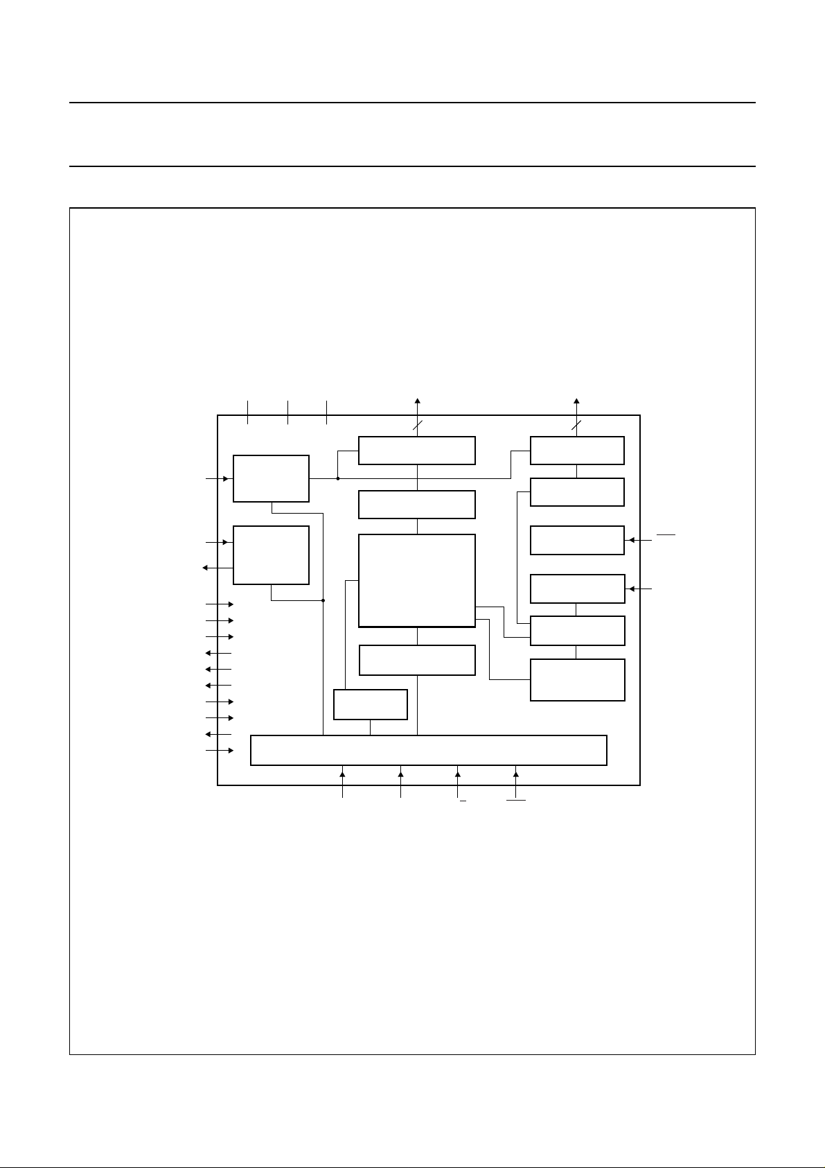
5 BLOCK DIAGRAM
6 PINNING
7 PIN FUNCTIONS
7.1 ROW 0 to ROW 47 row driver outputs
7.2 COL 0 to COL 83 column driver outputs
7.3 V
7.4 V
7.5 V
and V
SS1
DD1
LCDOUT, VLCDIN
to V
SS2
: positive power supply rails
DD3
: negative power supply rails
and V
LCDSENSE
: LCD power
supplies
7.6 V
OS0
to V
OS4
7.7 T1 to T7: test pads
7.8 SDIN: serial data line
7.9 SCLK: serial clock line
7.10 D/C: mode select
7.11 SCE: chip enable
7.12 OSC: oscillator
7.13 RES: reset
8 BLOCK DIAGRAM FUNCTIONS
8.1 Oscillator
8.2 Address counter (AC)
8.3 Display Data RAM (DDRAM)
8.4 Timing generator
8.5 Display address counter
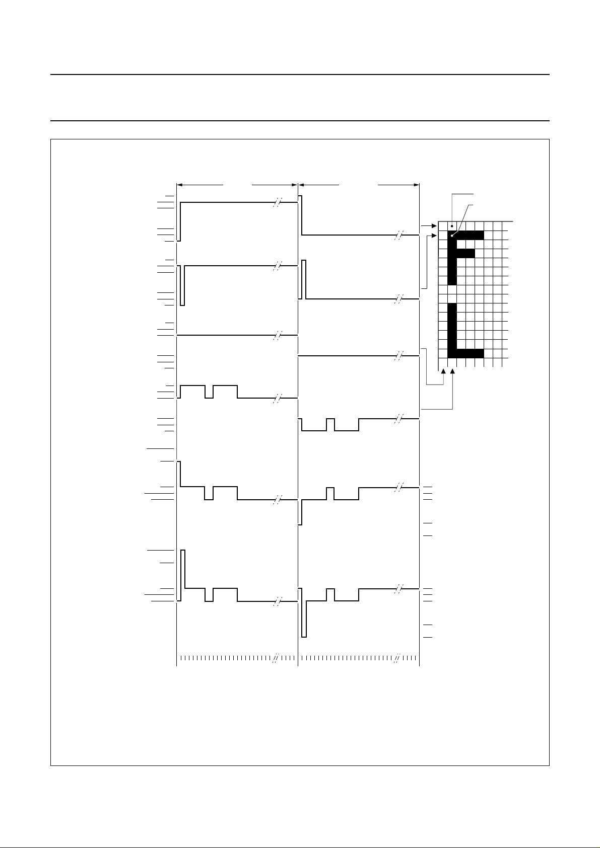
8.6 LCD row and column drivers
8.7 V
generator
LCD
9 INITIALIZATION
10 ADDRESSING
10.1 Data structure
11 INSTRUCTIONS
11.1 Reset function
11.2 Function set
11.2.1 PD
11.2.2 V
11.2.3 H
11.3 Display Control
11.3.1 D, E
11.4 Set Y address of RAM
11.5 Set X address of RAM
11.6 Temperature Control
11.7 Bias value:
11.8 V
generator
LCD
12 TEMPERATURE COMPENSATION
13 LIMITING VALUES
14 HANDLING
15 DC CHARACTERISTICS
16 AC CHARACTERISTICS
17 SERIAL INTERFACE
18 RESET
19 APPLICATION INFORMATION
20 MODULE MAKER PROGRAMMING
20.1 V
calibration
LCD
20.2 Charge pump multiplication factor
20.3 Bias system selected when BS[2:0] = 100
20.4 V
temperature coefficient selected when
LCD
TC[1:0] = 01 (TC1)
20.5 Seal bit
20.6 Module Maker parameter programming
20.7 Example of V
calibration flow
LCD
21 CHIP INFORMATION
22 BONDING PAD LOCATIONS
23 DEVICE PROTECTION DIAGRAM
24 TRAY INFORMATION
25 DEFINITIONS
26 LIFE SUPPORT APPLICATIONS
2001 Nov 07 2
Page 3

Philips Semiconductors Product specification
48 × 84 pixels matrix LCD driver OM6213
1 FEATURES
• Single-chip LCD controller/driver
• 48 row, 84 column outputs
• Display data RAM 48 × 84 bits
• On-chip:
– Generation of LCD supply voltage (external supply
also possible)
– Generation of intermediate LCD bias voltages
– Oscillator requires noexternal components (external
clock also possible).
• External reset (RES) input pin
• Serial interface maximum 4.0 Mbit/s
• CMOS compatible inputs
• Mux rate: 1 : 48
• Logic supply voltage range V
• Supply voltage range for high voltage part V
to VSS: 2.5 to 3.3 V
DD1
DD2
to VSS:
2.5 to 3.3 V
• Display supply voltage range V
to VSS: 4.5 to 9.0 V
LCD
• Low power consumption (typically 120 µA), suitable for
battery operated systems
• Temperature compensation of V
• Temperature range: T
amb
LCD
= −40 to +85 °C
• 5 Module Maker programmable parameters.
2 APPLICATIONS
• Telecommunications equipment.
3 GENERAL DESCRIPTION
The OM6213 is a low power CMOS LCD controller driver,
designed to drive a graphic display of 48 rows and
84 columns. All necessary functions for the display are
provided in a single chip, including on-chip generation of
LCD supply and bias voltages, resulting in a minimum of
external components and low power consumption. The
OM6213 interfaces to microcontrollers via a serial bus
interface.
4 ORDERING INFORMATION
PACKAGE
TYPE NUMBER
NAME DESCRIPTION VERSION
OM6213U TRAY chip with bumps in tray −
2001 Nov 07 3
Page 4
Philips Semiconductors Product specification
48 × 84 pixels matrix LCD driver OM6213
5 BLOCK DIAGRAM
V
handbook, full pagewidth
DD1
V
DD2VDD3
COL 0 to COL 83
ROW 0 to ROW 47
V
LCDIN
V
LCDSENSE
V
LCDOUT
V
V
V
OS
SS1
SS2
[
4:0
T1
T2
T3
T4
T5
T6
T7
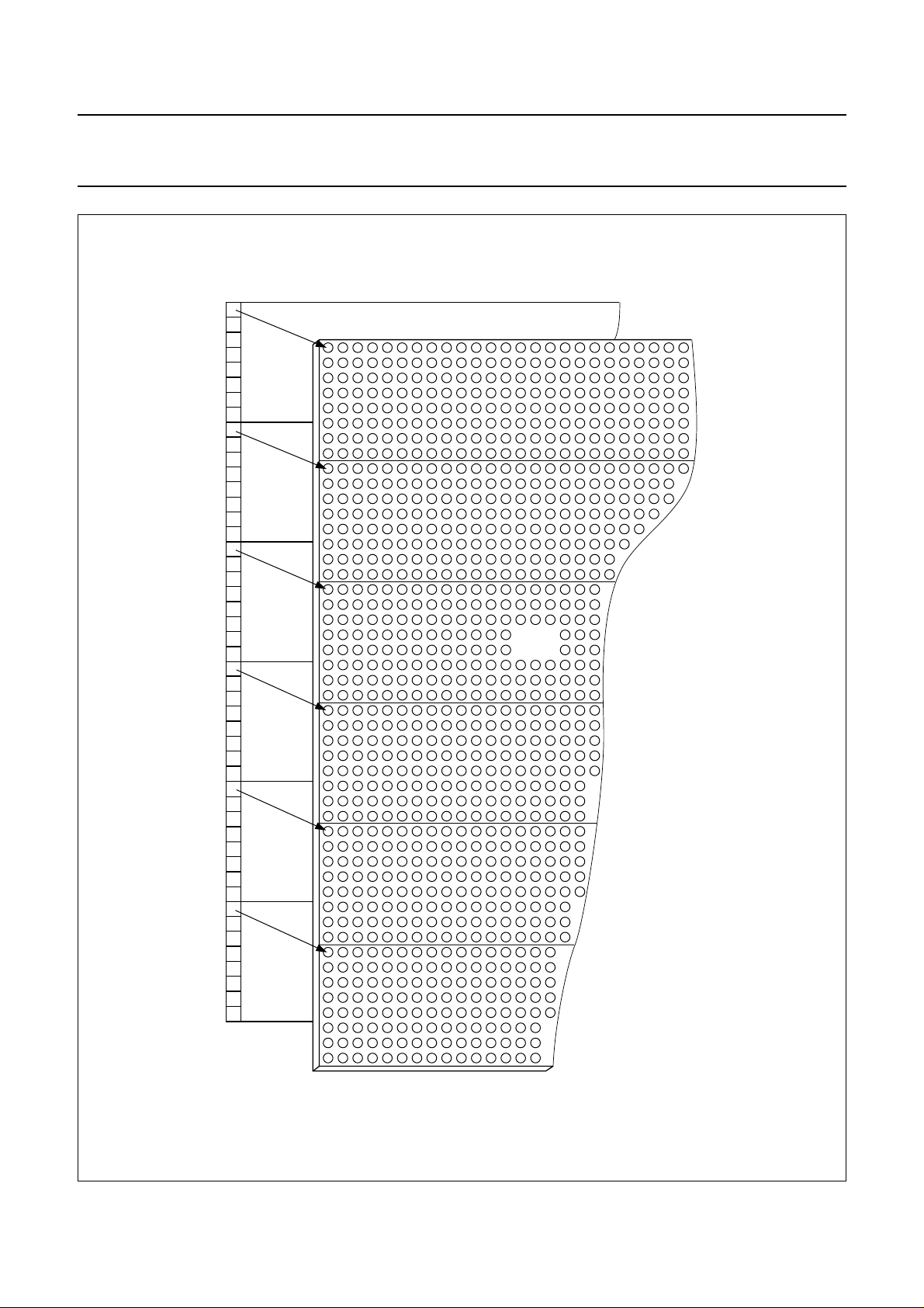
]
BIAS
VOLTAGE
GENERATOR
V
LCD
GENERATOR
COLUMN DRIVERS
DATA LATCHES
DISPLAY DATA RAM
(DDRAM)
48 × 84 bits
ADDRESS COUNTER
DATA
REGISTER
SDIN SCLK
84
I/O BUFFER
OM6213
D/C
ROW DRIVERS
SHIFT REGISTER
OSCILLATOR
GENERATOR
SCE
48
RESET
TIMING
DISPLAY
ADDRESS
COUNTER
RES
OSC
MGT840
Fig.1 Block diagram.
2001 Nov 07 4
Page 5

Philips Semiconductors Product specification
48 × 84 pixels matrix LCD driver OM6213
6 PINNING
SYMBOL PAD DESCRIPTION
V
V
V
V
V
V
V
V
OS4
OS3
OS2
OS1
OS0
DD1
DD3
DD2
3V
4V
5V
6V
7V
13 to 18 supply voltage 1
19 to 22 supply voltage 3
23 to 30 supply voltage 2
offset pad 0 input
LCD
offset pad 1 input
LCD
offset pad 2 input
LCD
offset pad 3 input
LCD
offset pad 4 input
LCD
SCLK 31 serial clock input
T7 32 to 35 test 7 alternative HV-gen
programming input
SDIN 36 to 39 serial data input and HV-gen
programming input
D/
C 40 data/command input
SCE 41 chip enable input (active
LOW)
OSC 42 oscillator input
V
SS2
43 to 50 ground 2
T4 51 test 4 input
T5 52 test 5 input
T6 53 test 6 output
V
SS1
54 to 61 ground 1
SYMBOL PAD DESCRIPTION
T1 62 test 1 output
T2 63 test 2 output
T3 64 test 3 output
V
LCDIN
65 to 70 V
supply voltage input and
LCD
HV-gen programming input
V
LCDOUT
V
LCDSENSE
71 to 77 V
78 V
generator output
LCD
generator regulation
LCD
input
RES 79 reset input (active LOW)
ROW 11 to
89 to 100 LCD row driver outputs
ROW 0
ROW 12 to
101 to 112 LCD row driver outputs
ROW 23
COL 0 to
113 to 196 LCD column driver outputs
COL 83
ROW 47 to
197 to 208 LCD row driver outputs
ROW 36
ROW 24 to
209 to 220 LCD row driver outputs
ROW 35
1,8 to 12,
dummy pads
81 to 88,
221 and
222
7 PIN FUNCTIONS
7.1 ROW 0 to ROW 47 row driver outputs
These pads output the row signals.
7.2 COL 0 to COL 83 column driver outputs
These pads output the column signals.
7.3 V
V
SS1
SS1
andV
and V
mustbe connected together, jointly referred
SS2
: negative power supply rails
SS2
to as VSS. When a pin has to be connected externally to
VSS, V
7.4 V
V
DD1
analog supply; jointly referred to as V
should be used.
SS1
DD1
to V
: positive power supply rails
DD3
provides the logic supply. V
DD2
and V
DD2
. V
DD3
DD2
provide the
and V
DD3
must be connected together.
2001 Nov 07 5
7.5 V
LCDOUT, VLCDIN
and V
LCDSENSE
: LCD power
supplies
If the internal V
be connected together. If not (the internal V
generator is used, then all 3 pins must
LCD
LCD
generator
is disabled and an external voltage is supplied at pin
V
), V
LCDIN
LCDOUT
must be connected to V
switch-off the charge pump if an external V
is used. V
7.6 V
LCDIN
OS0
Five input pins for on-glass V
connected to V
V
, which corresponds to logic 1. All five pins define a
DD1
must be left open-circuit and V
LCDIN.VPR
must be set to logic 0to
generator
LCD
is also used for HV-gen programming.
to V
OS4
offset. Each pin must be
LCD
, which corresponds to logic 0, or to
SS1
LCDSENSE
5-bit two’s complement number ranging from −16 to +15
decimal (from 10000 to 01111). The default value, with all
pins connected to V
, is 0 decimal (00000). The register
SS1
is refreshed by each set bias system command or when
exiting the Power-down mode.
Page 6

Philips Semiconductors Product specification
48 × 84 pixels matrix LCD driver OM6213
7.7 T1 to T7: test pads
In the application, T4, T5 and T7 must be connected to
VSS. T1, T2, T3 and T6 must be left open-circuit.
7.8 SDIN: serial data line
Data line and HV-gen programming input.
7.9 SCLK: serial clock line
Input for the clock signal. 0 to 4.0 Mbits/s.
7.10 D/C: mode select
Input to select either command/address or data input.
7.11 SCE: chip enable
The enable pin allows data to be clocked in; this signal is
active LOW.
7.12 OSC: oscillator
If the on-chip oscillator is used, this input must be
connected to V
connected to pin OSC. If pin OSC is left at V
. If an external clock is used, it must be
DD1
, the
SS1
internal clock isdisabled, the deviceis not clocked and the
display may be left in a DC state. To avoid this, it is
advisable to enter the Power-down mode before stopping
the clock.
8.3 Display Data RAM (DDRAM)
The OM6213 contains a 48 × 84 bit static RAM which
storesthe display data.The RAM is dividedinto 6 banks of
84 bytes (6 × 8 × 84 bits). During RAM access, data is
transferred to the RAM via the serial interface. There is a
direct correspondence between the X address and the
column output number.
8.4 Timing generator
The timing generator produces the various signals
required to drive the internal circuitry. Internal chip
operation is not affected by operations on the data bus.
8.5 Display address counter
The display is generated by continuously shifting rows of
RAM data to the dot matrix LCD via the column outputs.
The display status (all dots on/off and normal/inverse
video) is set by bits D and E in the command ‘Display
control’ (see Table 2).
8.6 LCD row and column drivers
The OM6213 contains 48 rows and 84 column drivers,
which connect the appropriate LCD bias voltages in
sequence to the display in accordance with the data to be
displayed. Figure 2 shows typical waveforms. Unused
outputs should be left unconnected.
7.13 RES: reset
This signal will reset the device and must be applied to
properly initialize the chip; this signal is active LOW.
8 BLOCK DIAGRAM FUNCTIONS
8.1 Oscillator
The on-chip oscillator provides the clock signal for the
display system. No external components are required and
the OSC input must be connected to V
. If an external
DD1
clock signal is used, it must be connected to pin OSC.
8.2 Address counter (AC)
The address counter assigns addresses to the display
data RAM for writing. The X address X[6:0] and the
Y addressY[2:0] are set separately. Afterawrite operation
the address counter is automatically incremented by 1
according to the V flag.
8.7 V
generator
LCD
The voltage multiplier (i.e. charge pump) generates the
V
voltage. The multiplication factor is Module Maker
LCD
programmable (default value 4).
2001 Nov 07 6
Page 7
Philips Semiconductors Product specification
48 × 84 pixels matrix LCD driver OM6213
ROW 0
R0 (t)
ROW 1
R1 (t)
COL 0
C0 (t)
COL 1
C1 (t)
V
V3 − V
LCD
V
V
V
V
V
V
V
V
V
V
V
V
V
V
V
V
V
V
V
V
V
V
V
V
SS1
LCD
2
3
4
5
SS1
LCD
2
3
4
5
SS1
LCD
2
3
4
5
SS1
LCD
2
3
4
5
SS1
frame n frame n + 1
V
state1
V
state2
(t)
(t)
V
state1
V
state2
(t) = C1(t) − R0(t)
V
state1
V
(t) = C1(t) − R1(t)
state2
V
− V
LCD
0 V
V3 − V
V
LCD
V3 − V
V
LCD
0 V
V3 − V
2
SS1
− V
2
2
2
012345678... ... 47 012345678... ... 47
(t)
(t)
V4 − V
0 V
V
SS1
V4 − V
− V
LCD
V4 − V
0 V
V
SS1
V4 − V
− V
LCD
MGT841
5
− V
LCD
5
− V
LCD
5
5
Fig.2 Typical LCD driver waveforms.
2001 Nov 07 7
Page 8
Philips Semiconductors Product specification
48 × 84 pixels matrix LCD driver OM6213
DDRAM
bank 0
top of LCD
R0
bank 1
R8
bank 2
bank 3
bank 4
bank 5
R16
LCD
R24
R32
R40
Fig.3 DDRAM to display mapping.
2001 Nov 07 8
R47
MGT842
Page 9
Philips Semiconductors Product specification
48 × 84 pixels matrix LCD driver OM6213
9 INITIALIZATION
Immediately following power-on, all internal registers and
the RAM content are undefined. A reset (RES)pulse must
be applied. It should be noted that the device may be
damaged if not properly reset.
Reset is accomplished by applying an external RES pulse
(active LOW) at pad RES. When reset occurs within the
specified time, all internal registers are reset, however the
RAM is still undefined. The state after reset is described in
Section “Reset function”.
RES input must be ≤ 0.3V
V
(or higher) according to t
DD(min)
DD1
after V
VHRL
reaches
DD1
timing (see
Fig.16).
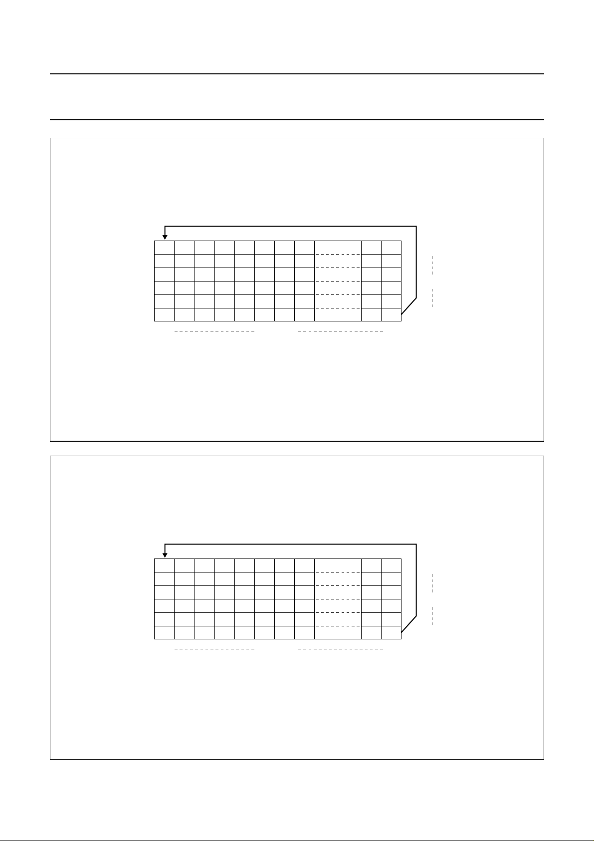
10 ADDRESSING
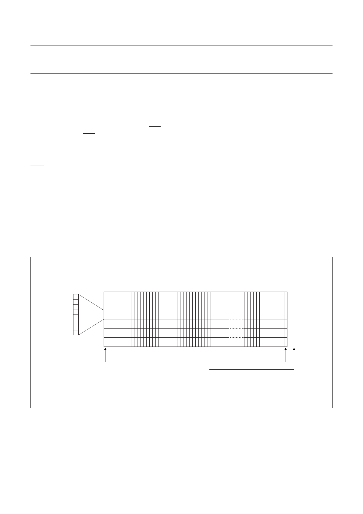
Data is downloaded in bytes into the RAM matrix of the
OM6213 as indicated in Figs.3, 4, 5 and 6. The display
RAM has a matrix of 48 × 84 bits. The columns are
addressed by the address pointer.
10.1 Data structure
The address ranges are: X=0to83 (1010011) and
Y = 0 to 5 (101). Addresses outside these ranges are not
allowed.
In vertical addressing mode (V = 1) the Y address
increments after each byte (see Fig.5). After the last
Y address (Y = 5) Y wraps around to 0 and X increments
to address the next column.
In horizontal addressing mode (V = 0) the X address
increments after each byte; see Fig.6. After the last
X address (X = 83) X wrapsaround to 0 andY increments
to address the next row.
After the very last address (X = 83 and Y = 5) the address
pointers wrap around to address (X = 0 and Y = 0).
handbook, full pagewidth
LSB
MSB
0 83X address
Y address
Fig.4 RAM format, addressing.
0
5
MGT843
2001 Nov 07 9
Page 10
Philips Semiconductors Product specification
48 × 84 pixels matrix LCD driver OM6213
handbook, full pagewidth
06
17
2
3
4
5
083X address
0
Y address
5503
MGT844
Fig.5 Sequence of writing data bytes into RAM with vertical addressing (V = 1).
handbook, full pagewidth
012
84 85 86
168 169 170
252 253 254
336 337 338
420 421 422
083X address
Fig.6 Sequence of writing data bytes into RAM with horizontal addressing (V = 0).
2001 Nov 07 10
0
Y address
5503
MGT845
Page 11

Philips Semiconductors Product specification
48 × 84 pixels matrix LCD driver OM6213
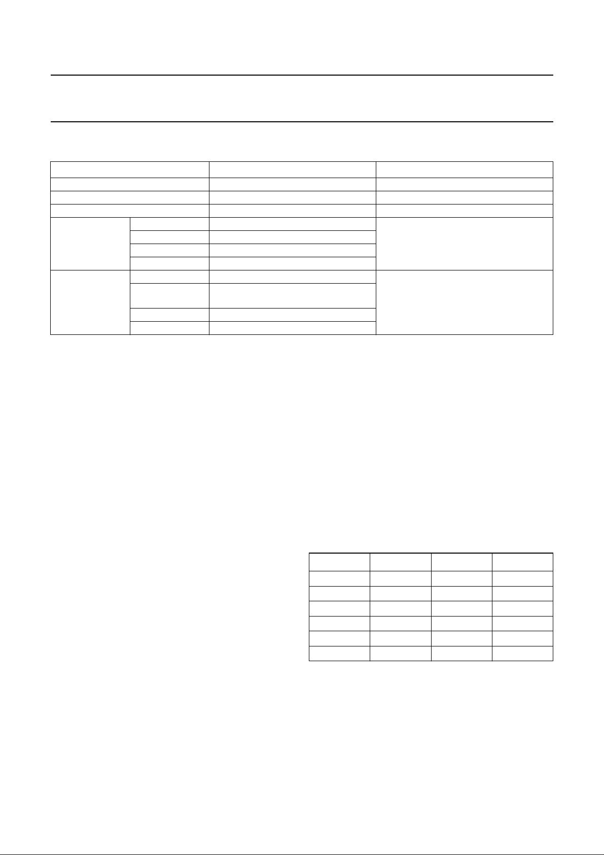
11 INSTRUCTIONS
The instruction format is divided into two modes. If D/C
(mode select) isset LOW the current byte is interpretedas
command byte (see Table 1). If D/C is set HIGH the
following bytes are stored in the DDRAM. After every data
byte the address counter is incremented automatically.
The level of the D/C signal is read during the last bit of the
data byte.
Instructions can be sent in any order to the OM6213 (the
exception being that the temperature control command
mustbefollowed by at least onebyteofdata or command).
TheMSBis transmitted first (see Fig.7).Figure 8showsan
example of a command stream, used to set-up the LCD
driver.
The serial interfaceis initialized whenSCE is HIGH. In this
state SCLK clock pulses have no effect and no power is
consumedby the serialinterface. A negativeedge on SCE
enablestheserial interface and indicates the startofadata
transmission.
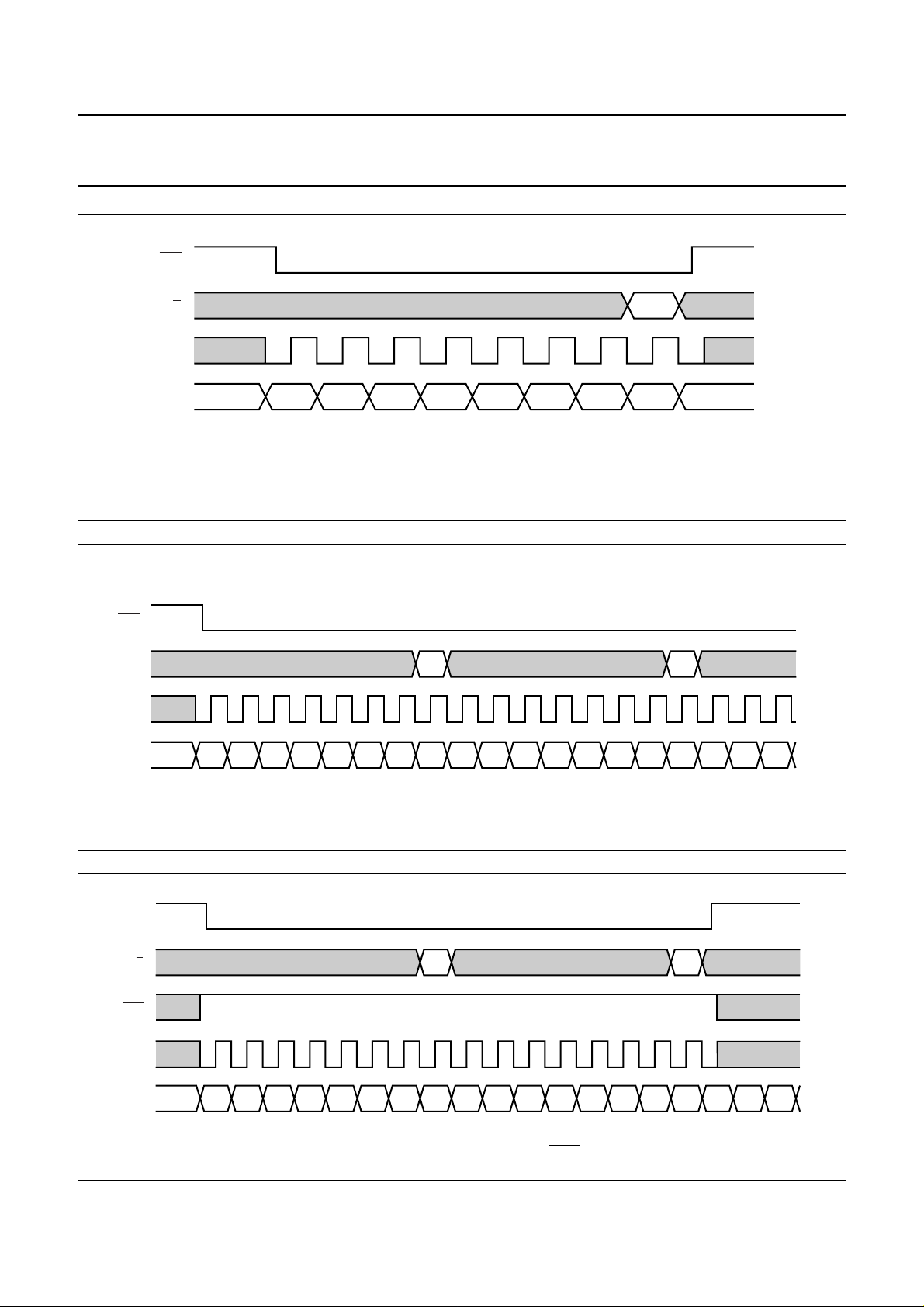
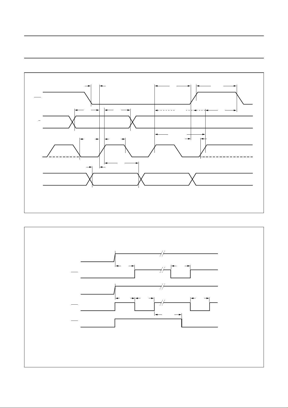
Figures 9 and 10 show the serial bus protocol.
• When SCE is HIGH, SCLK clocks are ignored. During
the HIGH time of SCE the serial interface is initialized
(see Fig.11).
• SDIN is sampled at the positive edge of SCLK
• D/C indicates whether the byte is a command (D/C=0)
or RAM data (D/C = 1). It is read with the eighth SCLK
pulse.
• If SCE stays LOW after the last bit of a command/data
byte,the serial interfaceexpects bit DB7 ofthe next byte
at the next rising edge of SCLK (see Fig.11)
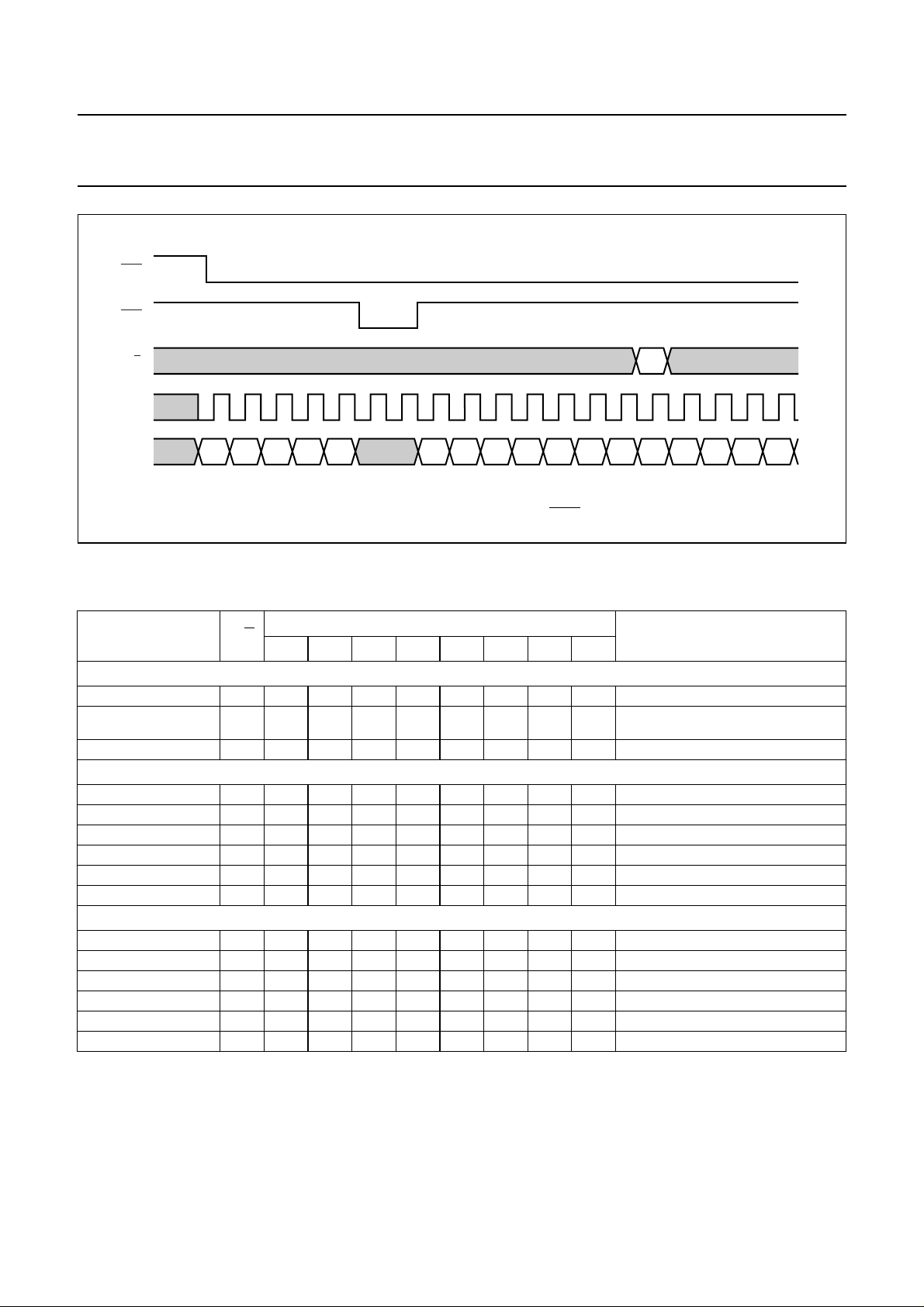
• A reset pulse with RES interrupts the transmission. The
data being written into the RAM may be corrupted. The
registers are cleared. If SCE is LOW after the rising
edge of RES, the serial interface is ready to receive the
D/C bit of a command/data byte (see Fig.12).
• Instructions (except the temperature control command)
are executed on the SCLK positive edge which latches
DB0 and D/C
• The temperature control command is executed on the
SCLK positive edge which latches DB0 and D/C of the
next command or the next write to the DDRAM
(whichever occurs first).This command requires 2 bytes
to be executed.
handbook, full pagewidth
handbook, halfpage
MSB (DB7) LSB (DB0)
Fig.7 General format of data stream.
bias systemfunction set (H = 1)
datadata
MGT639
set V
PR
temperature control
Fig.8 Serial data stream, example.
X addressY addressdisplay controlfunction set (H = 0)
MGT846
2001 Nov 07 11
Page 12
Philips Semiconductors Product specification
48 × 84 pixels matrix LCD driver OM6213
handbook, full pagewidth
handbook, full pagewidth
SCE
D/C
SCLK
SDIN
SCE
D/C
DB7 DB6 DB5 DB4 DB3 DB2 DB1 DB0
MGT641
Fig.9 Serial bus protocol; transmission of one byte.
SCLK
SDIN DB7 DB6 DB5 DB4 DB3 DB2 DB1 DB0 DB7DB7 DB6 DB5 DB4 DB3 DB2 DB1 DB0
Fig.10 Serial bus protocol; transmission of several bytes.
handbook, full pagewidth
SCE
D/C
RES
SCLK
SDIN DB7 DB6 DB5 DB4 DB3 DB2 DB1 DB0 DB7DB7 DB6 DB5 DB4 DB3 DB2 DB1 DB0
Fig.11 Serial bus reset function (SCE).
DB6 DB5
MGT642
DB6 DB5
MGT643
2001 Nov 07 12
Page 13
Philips Semiconductors Product specification
48 × 84 pixels matrix LCD driver OM6213
handbook, full pagewidth
SCE
RES
D/C
SCLK
SDIN DB7 DB6 DB5 DB4 DB3 DB7DB7 DB6 DB5 DB4 DB3 DB2 DB1 DB0
DB6 DB5 DB4
MGT644
Fig.12 Serial bus reset function (RES).
Table 1 Instruction set; see note 1 and Table 2
Instructions not expressly defined in Table 1 and reserved instructions must not be used in the application.
COMMAND BYTE
INSTRUCTION D/
C
DESCRIPTION
DB7 DB6 DB5 DB4 DB3 DB2 DB1 DB0
(H=0or1)
NOP
Function set
Write data
000000000
000100PDVH
1D7D6D5D4D3D2D1D
no operation
Power-down control; entry mode;
extended instruction set control (H)
writes data to display RAM.
0
(H=0)
Reserved
Reserved
Display control
Reserved
Set Y address of RAM
Set X address of RAM.
00000001X
0000001XX
000001D0E
00001XXXX
001000Y
01X
6
X
5
X
4
X
3
2
X
2
Y
1
X
1
reserved
reserved
sets display configuration
reserved
sets Y address of RAM; 0 ≤ Y ≤ 5
Y
0
Sets X address part of RAM; 0 ≤ Y ≤ 5
X
0
(H=1)
Reserved
Temperature control
Reserved
Bias system
Reserved
Set V
PR
00000001X
0000001TC
1TC0
000001XXX
000010BS
2BS1
001XXXXXX
01V
PR6VPR5VPR4VPR3VPR2VPR1VPR0
reserved
set temperature coefficient (TCx)
reserved
set bias system (BSx)
BS
0
reserved
write VPR to register
Note
1. X = don’t care.
2001 Nov 07 13
Page 14
Philips Semiconductors Product specification
48 × 84 pixels matrix LCD driver OM6213
Table 2 Explanations for symbols in Table 1
BIT LOGIC 0 LOGIC 1
PD chip is active chip is in Power-down mode
V horizontal addressing vertical addressing
H use basic instruction set use extended instruction set
D, E 00 display blank
10 normal mode
01 all display segments on
11 inverse video mode
TC1 and TC0 00 (TC0) V
01 (TC1)
10 (TC2) V
11 (TC3) V
temperature coefficient TCA
LCD
Module Maker defined;
V
temperature coefficient
LCD
temperature coefficient TCC
LCD
temperature coefficient TCD
LCD
11.1 Reset function
After reset the LCD driver has the following state:
• Power-down mode (PD = 1)
• Horizontal addressing (V = 0) normal instruction set
(H=0)
• Display blank (E = D = 0)
• Address counter X[6:0] = 0, Y[2:0] = 0
• Temperature control mode (TC[1:0] = 0, TC0, TCA)
• Bias system (BS[2:0] = 0)
• V
is equal to 0, the HV-generator is switched off
LCD
(VPR[6:0] = 0)
• After power-on, RAM data is undefined
• Oscillator off (external clock operation is possible).
11.2 Function set
11.2.1 PD
• All LCD outputs at V
• Bias generator and V
(display off)
SS1
generator off, V
LCD
LCD
can be
disconnected
• Oscillator off
• Serial bus, command, etc. function
• RAM contents not cleared; RAM data can be written.
11.2.2 V
When V = 0, horizontal addressing is selected. Thedata is
written into the DDRAM as shown in Fig.6. When V = 1,
vertical addressing is selected. The data is written into the
DDRAM as shown in Fig.5.
11.2.3 H
When H = 0 the commands ‘display control’, ‘set
Y address’ and ‘set X address’ can be performed, when
H = 1 the others can be executed. The commands ‘write
data’ and ‘function set’ can be executed in both cases.
11.3 Display Control
11.3.1 D, E
The bits D and E select the display mode (see Table 2).
11.4 Set Yaddress of RAM
Y2 to Y0 defines the Y address vector address of the
display RAM; see Table 3.
Table 3 Yaddress range
Y2 Y1 Y0 CONTENT
0 0 0 bank 0
0 0 1 bank 1
0 1 0 bank 2
0 1 1 bank 3
1 0 0 bank 4
1 0 1 bank 5
11.5 Set X address of RAM
The X address points to the columns. The range of X is
0 to 83 (53H).
11.6 Temperature Control
The temperature coefficient of V
is selected by the two
LCD
bits TC1 and TC0.
2001 Nov 07 14
Page 15

Philips Semiconductors Product specification
48 × 84 pixels matrix LCD driver OM6213
11.7 Bias value
The bias voltage levels are set in the ratio of R - R - nR - R - R giving a bias system. Different multiplex rates
1
----------------n4+()
require different factors of ‘n’ (see Table 4). This is programmed by BS[2:0]. For Mux 1 : 48 the optimum bias value ‘n’ is
1
given by resulting in
n483–3.928 4===
⁄8bias.
Table 4 Programming the required bias system
BS2 BS1 BS0
0007
0016
0105
0114
100−Module Maker
n BIAS SYSTEM RECOMMENDED MUX RATE
1
⁄
11
1
⁄
10
1
⁄
9
1
⁄
8
1 : 100
1:80
1:65
1:48
−
programmable
(see Table 11)
1012
1101
1110
1
⁄
6
1
⁄
5
1
⁄
4
1:24
1:18/1:16
1:10/1:9/1:8
Table 5 LCD bias voltage
SYMBOL BIAS VOLTAGE FOR1⁄8 BIAS SYSTEM
V1 V
V2
V3
V4
V5
V6 V
7
⁄8× V
6
⁄8× V
2
⁄8× V
1
⁄8× V
LCD
LCD
LCD
LCD
LCD
SS
2001 Nov 07 15
Page 16

Philips Semiconductors Product specification
48 × 84 pixels matrix LCD driver OM6213
11.8 V
Thebinary number V
generator
LCD
representingthe operating voltage
OP
can be set by the serial interface command and can be
adjusted (calibrated) by 5 input pins according to the
following formulae:
V
OP
V
OSVCAL
2V
×()++=
PR
(1)
where:
• V
is an 8-bit unsigned number used internally for
OP
generation of the LCD supply voltage V
LCD
• VOS is a 5-bit two’s complement number set by the
5 input pins VOS[4:0]; see Table 6
• V
is a 5-bit two’s complement number set by the
CAL
Module Maker; see Table 7
• VPRisa7-bit unsigned number set bytheserialinterface
command.
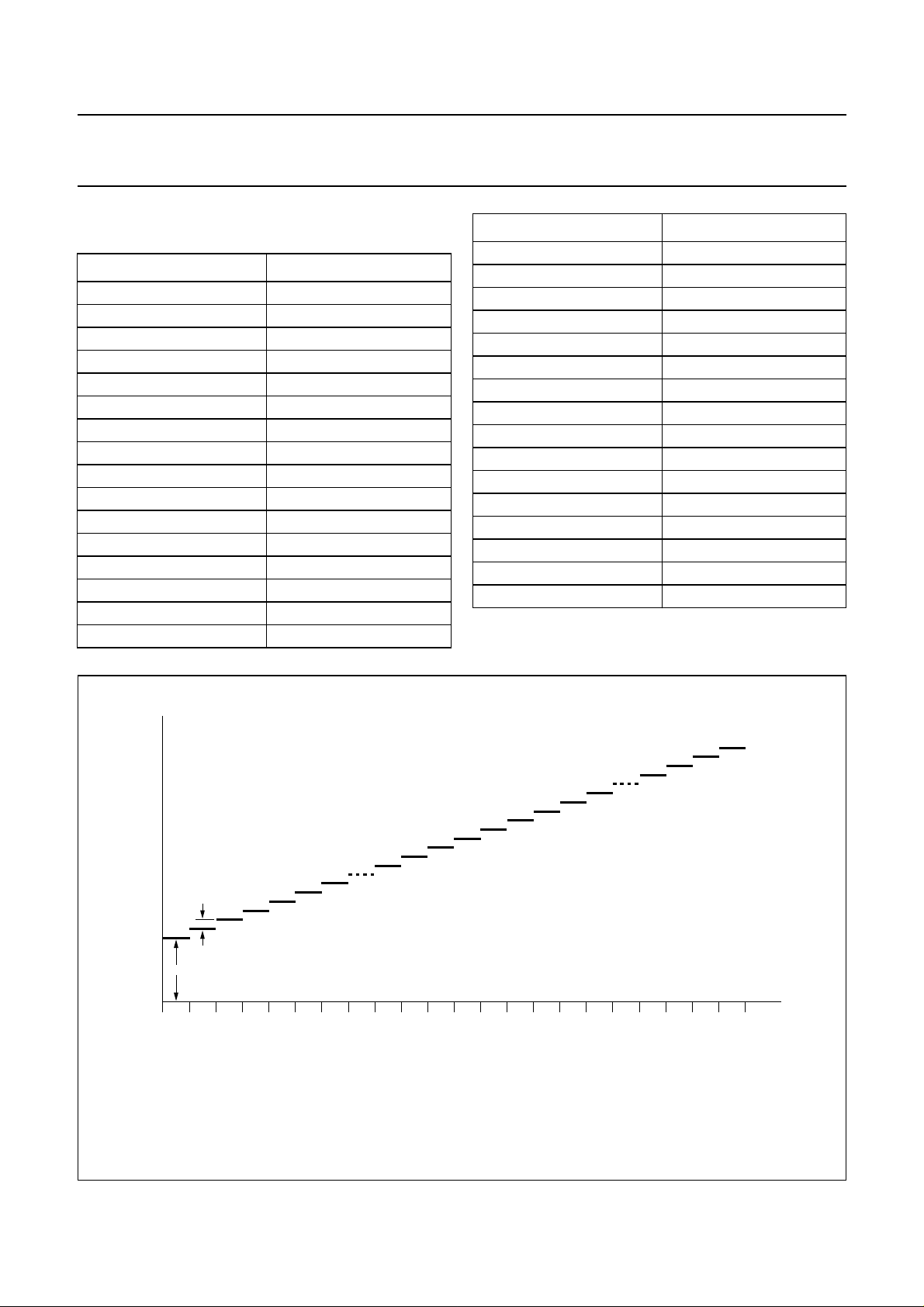
To avoid numerical overflow the allowed values of V
should be limited to the range V
PR(min)
to V
PR(max)
PR
(decimal).
The corresponding voltage at the reference temperature,
T
, can be calculated as:
CUT
V
LCD Tcut()
aVOPb×+()=
(2)
The generated voltage at V
is dependent on the
LCD
temperature, programmed temperature coefficient (TC)
and the programmed voltage at thereference temperature
(T
).
CUT
V
LCD
,a and b for eachtemperature coefficient aregiven in
T
CUT
aVOPb×+()1TC TT
–()×+[]×=
CUT
(3)
Table 6. The maximum voltage that can be generated is
dependent on the voltage of V
and the display load
DD2
current.
Astheprogramming range for the internally generated
V
allows values above the maximum allowed V
LCD
LCD
the user has to ensure while setting the VPR register
and selecting the Temperature Compensation (TC),
that under all conditions and including all tolerances
the V
Fora particular liquid,the optimum V
limit of maximum 9 V will never be exceeded.
LCD
canbe calculated
LCD
for a given multiplex rate. For a mux rate of 1 : 48, the
optimum operating voltage of the liquid can be calculated
as follows;
where V
V
LCD
is the threshold voltage of theliquid crystal used.
th
148+
------------------------------------21
⋅
1
–
----------
48
6.06 Vth⋅=⋅=
V
th
(4)
,
Table 6 Typical values for parameters of the HV generator programming
SYMBOL TCA TCB TCC TCD UNIT
a 3.06 3.84 3.62 3.37 V
b 30.3 24.3 26.1 28.0 mV
T
CUT
27 27 27 27 °C
TC 0 −0.87 −0.58 −0.29 10
V
PR(min)
V
PR(max)
V
LCD(min)
V
LCD(max)
V
LCD(min)
V
LCD(max)
V
LCD
values are the values corresponding to V
values are the theoretical values corresponding to V
must never exceed 9 V.
Example: VPR is set to 63 (decimal) and TCB is selected. At temperature T
wants to decrease V
LCD
49 20 30 39 decimal
127 101 110 120 decimal
6.04 4.81 5.18 5.56 V
10.77 8.74 9.35 10.11 V
.
PR(min)
. Under all conditions and including all tolerances
PR(max)
by 100 mV in order to set V
the measured V
CUT
to 6.8 V. The best value for VOSis then −4 decimal (11100 binary
LCD
is 6.9 V. The user
LCD
in the two’s complement notation).
If VPR[6:0] is set to zero, the charge pump is turned off.
-3
/°C
2001 Nov 07 16
Page 17
Philips Semiconductors Product specification
48 × 84 pixels matrix LCD driver OM6213
Table 7 VOS and V
notation
DECIMAL BINARY
0 00000
1 00001
2 00010
3 00011
4 00100
5 00101
6 00110
7 00111
8 01000
9 01001
10 01010
11 01011
12 01100
13 01101
14 01110
15 01111
values in two’s complement
CAL
DECIMAL BINARY
−1 11111
−2 11110
−3 11101
−4 11100
−5 11011
−6 11010
−7 11001
−8 11000
−9 10111
−10 10110
−11 10101
−12 10100
−13 10011
−14 10010
−15 10001
−16 10000
handbook, full pagewidth
V
LCD
b
a
00 01 02
VOP 7 to 0 programming (00H to FFH).
Depending on VPR restrictions defined in Table 6 and depending on VOS and V
If VPR is set to 0, the charge pump is turned off and V
03 04 05 06
Fig.13 V
. . . . . . FD FE FF
= 0 V if no external V
LCD
programming of the OM6213.
LCD
, not all VOP[7:0] can be selected.
CAL
supply is provided.
LCD
MGT847
V
OP
2001 Nov 07 17
Page 18
Philips Semiconductors Product specification
48 × 84 pixels matrix LCD driver OM6213
12 TEMPERATURE COMPENSATION
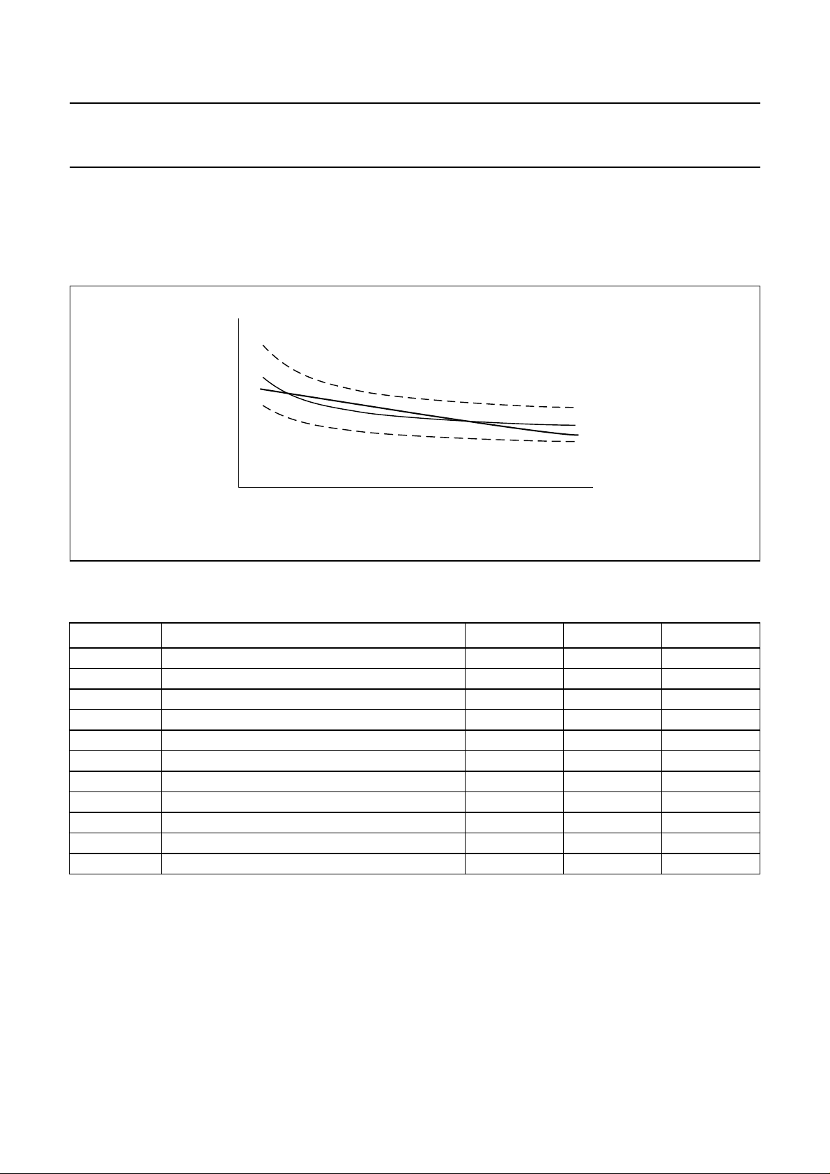
Due to the temperature dependency of the liquid crystal viscosity, the LCD controlling voltage V
with lower temperature to maintain optimum contrast. Figure 14. shows V
temperature coefficient of V
handbook, full pagewidth
V
can be selected from 4 values (see Table 2) by setting bits TC[1:0].
LCD
LCD
Fig.14 V
as a function of liquid crystal temperature (typical values).
LCD
for high multiplex rates. In the OM6213 the
LCD
MGT848
T
13 LIMITING VALUES
In accordance with the Absolute Maximum Rating System (IEC 60134); see notes 1 and 2.
must be increased
LCD
SYMBOL PARAMETER MIN. MAX. UNIT
V
DD1
V
DD2,3
V
LCD
V
i
I
SS
I
, I
I
P
tot
P
out
T
amb
T
jun
T
stg
o
logic supply voltage −0.5 +6.5 V
high supply voltage −0.5 +6.5 V
LCD supply voltage −0.5 +10 V
all input voltages −0.5 V
+ 0.5 V
DD1
ground supply current −50 +50 mA
DC input or output current −10 +10 mA
total power dissipation − 100 mW
power dissipation per output − 10 mW
ambient temperature −40 +85 °C
junction temperature −65 +150 °C
storage temperature −65 +150 °C
Notes
1. Stresses above those listed under Limiting Values may cause permanent damage to the device.
2. Parameters are valid over operating temperature range unless otherwise specified. All voltages are referenced to
unless otherwise noted.
V
SS1
14 HANDLING
Inputs and outputs are protected against electrostatic discharge in normal handling. However, to be totally safe, it is
desirable to take normal precautions appropriate to handling MOS devices (see
“Handling MOS devices”
).
2001 Nov 07 18
Page 19
Philips Semiconductors Product specification
48 × 84 pixels matrix LCD driver OM6213
15 DC CHARACTERISTICS
V
DD1=VDD2
SYMBOL PARAMETER CONDITIONS MIN. TYP. MAX. UNIT
V
DD1
V
DD2,3
V
LCD
I
DD1
I
DD2
I
DD3
I
LCDIN
Logic
V
IL
V
IH
I
LI
Column and row outputs
R
o(col)
R
o(row)
V
bias(col)
V
bias(row)
LCD supply voltage generator
V
LCD(tol)
= 2.5 to 3.3 V; VSS=0V; V
= 4.5 to 9.0 V; T
LCD
= −40 to +85 °C; unless otherwise specified.
amb
logic supply voltage 2.5 − 3.3 V
high supply voltage 2.5 − 3.3 V
LCD supply voltage note 1 4.5 − 9.0 V
total (V
DD1
+ V
supply current 1
DD2
+ V
)
normal mode;
DD3
V
DD1=VDD2=VDD3
V
= 6.9 V (4 booster device);
LCD
f
SCLK
= 0; T
amb
=25°C;
display load = 10µA; inputs at V
= 2.85 V;
DD1
or
− 120 −µA
VSS, bias system1⁄7; note 2
supply current 2 Power-down mode; with internal or
− 3 −µA
external LCD supply voltage; inputs at
V
or VSS; note 3
DD1
supply current external
V
LCD
V
DD1=VDD2=VDD3
V
= 6.9 V; f
LCD
SCLK
= 2.85 V;
= 0; T
amb
=25°C;
display load = 10 µA; inputs at V
DD1
− 20 −µA
or
VSS; bias system1⁄7; notes 2 and 5
supply current from
external V
LCD
V
DD1=VDD2=VDD3
V
= 6.9 V; f
LCD
SCLK
= 2.85 V;
= 0; T
amb
=25°C;
display load = 10 µA; inputs at V
DD1
− 25 −µA
or
VSS; bias system1⁄7; notes 2, 4 and 5
LOW-level input voltage V
SS
HIGH-level input voltage 0.7V
input leakage current Vi=V
column output resistance
note 6 − 420 kΩ
DD1
or V
SS
−1 − +1 µA
DD1
− 0.3V
− V
DD1
DD1
COL0 to COL83
row output resistance
note 6 − 420 kΩ
ROW0 to ROW47
bias tolerance COL0 to
−100 0 +100 mV
COL83
bias tolerance ROW0 to
−100 0 +100 mV
ROW47
V
tolerance internally
LCD
note 7 −70 − +70 mV
generated
V
V
2001 Nov 07 19
Page 20

Philips Semiconductors Product specification
48 × 84 pixels matrix LCD driver OM6213
Notes to the DC characteristics
1. Themaximum possible V
2. Internal clock.
3. Power-down mode: during Power-down all static currents are switched off.
4. If external V
5. V
external voltage applied to V
LCD
, the display load current is not transmitted to I
LCD
switch-off the charge pump.
6. Load current 10 µA, outputs tested one at a time.
7. Valid for values of temperature, VOP and TC used at the calibration.
16 AC CHARACTERISTICS
V
DD1=VDD2
= 2.5 V to 3.3 V; VSS=0V; V
SYMBOL PARAMETER CONDITIONS MIN. TYP. MAX. UNIT
f
clk(ext)
f
frame
t
VHRL
external clock frequency 30.9 34.3 37.7 kHz
frame frequency internal oscillator; note 1 63 70 77 Hz
reset LOW pulse set-up time
after power-on
t
RW
t
R(op)
reset LOW pulse width see Fig.16 100 −−ns
end of reset pulse to interface
being operational
Serial bus timing characteristics
f
SCLK
T
cy(SCLK)
t
PWH1
t
PWL1
t
S2
t
H2
t
PWH2
t
H5
t
S3
t
H3
t
S4
t
H4
clock frequency V
clock cycle time SCLK 250 −−ns
SCLK pulse width HIGH 100 −−ns
SCLK pulse width LOW 100 −−ns
SCE set-up time 60 −−ns
SCE hold time 100 −−ns
SCE minimum HIGH time 100 −−ns
SCE start hold time note 4 100 −−ns
D/C set-up time 100 −−ns
D/C hold time 100 −−ns
SDIN set-up time 100 −−ns
SDIN hold time 100 −−ns
voltage that maybe generated isdependent on voltage, temperature and (display) load.
LCD
DD.
LCDIN
and V
LCDSENSE
= 4.5 to 9.0 V; T
LCD
inputs; V
= −40 to +85 °C; unless otherwise specified.
amb
disconnected. VPR must be set to 0 to
LCDOUT
notes 2 and 3; see Fig.16 0 − 30 µs
−−1000 ns
= 3.0 V ±10%; all signal
DD1
0 − 4.00 MHz
timing is based on 20% to 80% of
VDD and a maximum rise and fall
time of 10 ns
Notes
1. t
frame=fclk(ext)
/490.
2. RES may be LOW before VDD goes HIGH (see Fig.16). This is recommended.
3. Decoupling capacitor V
LCD/VSS1
= 100 nF (higher capacitor size increases t
or higher V
VHRL
DD1,2,3
reduces t
VHRL
).
4. tH5is the time from the previous SCLK positive edge (irrespective of the state of SCE) to the negative edge of SCE
(see Fig.15).
2001 Nov 07 20
Page 21
Philips Semiconductors Product specification
48 × 84 pixels matrix LCD driver OM6213
17 SERIAL INTERFACE
handbook, full pagewidth
SCE
D/C
SCLK
SDIN
18 RESET
t
S3
t
PWL1
t
S2
t
H3
t
PWH1
t
t
S4
H4
t
H2
(tH5)
T
cy(SCLK)
t
PWH2
t
H5
t
S2
MGT849
Fig.15 Serial interface timing.
handbook, full pagewidth
V
RES
V
RES
SCE
DD1
DD1
t
RW
t
VHRL
t
RW
Fig.16 Reset timing.
2001 Nov 07 21
t
R(op)
t
RW
t
RW
MGT850
Page 22
Philips Semiconductors Product specification
48 × 84 pixels matrix LCD driver OM6213
19 APPLICATION INFORMATION
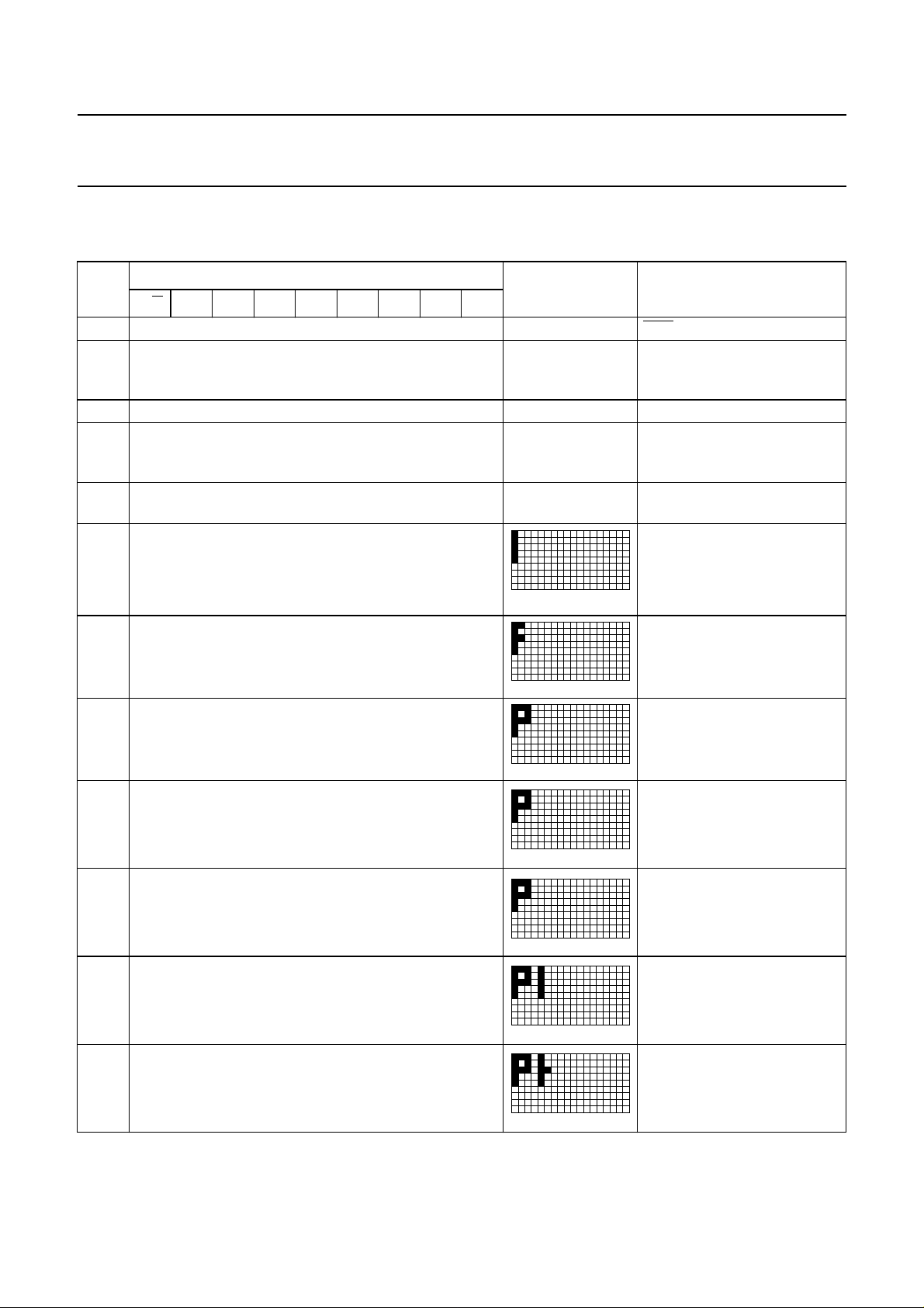
Table 8 Example of OM6213 operation
STEP
DISPLAY OPERATION
D/C DB7 DB6 DB5 DB4 DB3 DB2 DB1 DB0
SERIAL BUS BYTE
1 Start
SCE is going LOW
2 0 0 0 1 0 0 0 0 1 function set; PD = 0, V = 0,
select extended instruction set
(H = 1 mode)
3 0 1 0 0 1 0 0 0 0 set V
; VPR is set to 16
PR
4 0 0 0 1 0 0 0 0 0 function set; PD = 0, V = 0,
select normal instruction set
(H = 0 mode)
5 0 0 0 0 0 1 1 0 0 display control; set normal
mode (D = 1, E = 0)
6 1 0 0 0 1 1 1 1 1 data write; Yand X are
initialized to 0 by default, so
they are not set here
MGS405
7 1 0 0 0 0 0 1 0 1 data write
MGS406
8 1 0 0 0 0 0 1 1 1 data write
MGS407
9 1 0 0 0 0 0 0 0 0 data write
MGS407
10 1 0 0 0 1 1 1 1 1 data write
MGS408
11 1 0 0 0 0 0 1 0 0 data write
MGS409
12 1 0 0 0 1 1 1 1 1 data write
MGS410
2001 Nov 07 22
Page 23
Philips Semiconductors Product specification
48 × 84 pixels matrix LCD driver OM6213
STEP
D/
C DB7 DB6 DB5 DB4 DB3 DB2 DB1 DB0
DISPLAY OPERATION
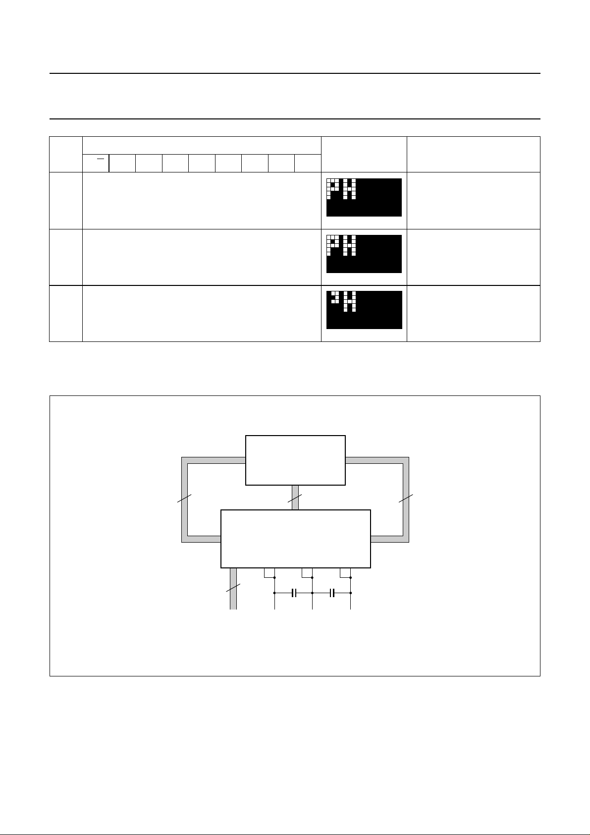
13 0 0 0 0 0 1 1 0 1 display control; set inverse
video mode (D = 1, E = 1)
SERIAL BUS BYTE
MGS412
14 0 1 0 0 0 0 0 0 0 set X address of RAM; set
address to 0000000
MGS412
15 1 0 0 0 0 0 0 0 0 data write
MGS414
The pinning of the OM6213 is optimized for single plane wiring e.g. for chip-on-glass display modules. Display size:
48 × 84 pixels.
handbook, full pagewidth
DISPLAY 48 × 84
8424 24
OM6213
6
I/O
V
DD
V
SS
V
LCD
C
ext
MGT851
Fig.17 Application diagram.
The required minimum value for the external capacitors in an application with the OM6213 are:
= 100 nF (min.) for V
C
ext
LCD1,2/VSS1,2
, C
= 1.0 µF (min.) for V
ext
LCD1,2,3/VSS1,2
Higher capacitor values are recommended for ripple reduction.
2001 Nov 07 23
Page 24
Philips Semiconductors Product specification
48 × 84 pixels matrix LCD driver OM6213
20 Module Maker programming
The OM6213 features five Module Maker programmable
parameters:
1. V
calibration
LCD
2. Charge pump multiplication factor
3. Bias system selected when BS[2:0] = 100
4. V
temperature coefficient selected when
LCD
TC[1:0] = 01 (TC1)
5. Seal bit. Used to select the use of the default
parameters or the Module Maker programmable
parameters. Once set:
a) The seal bit cannot be reset
b) The Module Maker programmable parameters
cannot be changed
c) The Module Maker programmable parameters are
selected and the default parameters are
deselected.
20.1 V
The first parameter calibrates the V
A 5-bit code (V
calibration
LCD
CAL
voltage.
LCD
[4:0]) is used for this parameter. The
code is implemented in two’s complement notation giving
rise to a positive or negative offset to the VPR register.
V
calibration may be used together with V
LCD
(performed by connecting the VOS[4:0] pads to either V
or to V
DD1
).
LCD
offset
SS1
VPR values must always be within the ranges specified in
Table 6.
OP
V
LCD
V
OSVCAL
aVOPb at×+= T
V
canbe calculated fromequations(5) and (6):a and b
V
LCD
2V
×()++=
PR
nom
(5)
(6)
are parameters defined in Table 6. An example of the
correspondence between the V
V
calibration is shown in Table 9, where b is assumed
LCD
code and the relative
CAL
to be 24.3 mV(TCB, temperature coefficient B) andVOSis
assumed to be 0.
handbook, full pagewidth
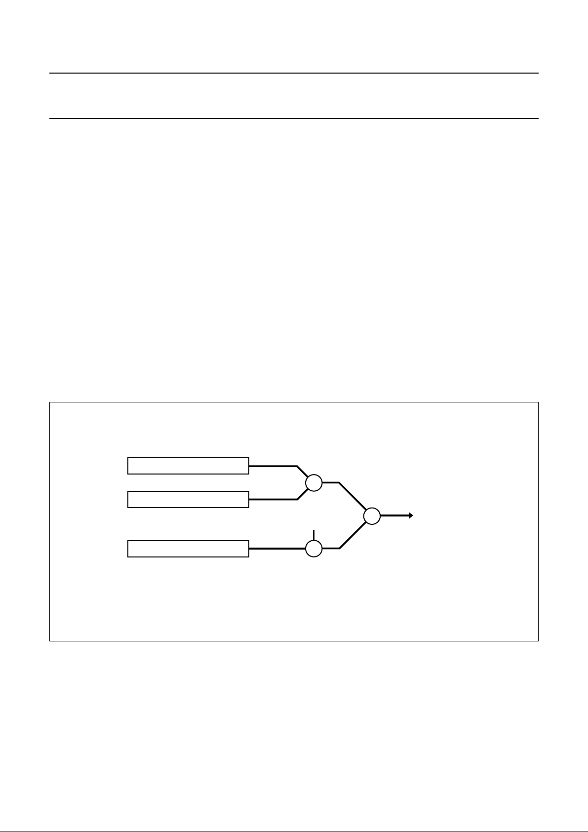
V
offset: 5-bit signed value
LCD
[
]
4:0
V
OS
V
calibration: 5-bit signed value
LCD
[
]
4:0
V
CAL
VPR register: 7-bit unsigned value
[
]
6:0
V
PR
−16 to +15
−16 to +15
0 to +127
Fig.18 V
+
2
×
offset and calibration
LCD
V
OP
+
to high voltage
generator
MGT852
2001 Nov 07 24
Page 25
Philips Semiconductors Product specification
48 × 84 pixels matrix LCD driver OM6213
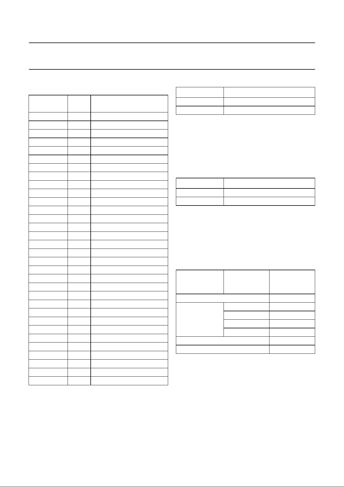
Table 9 V
V
CAL
codes and associated nominal calibration
CAL
voltage (TCB, V
[4:0] V
CAL
OS
=0)
V
CALIBRATION (mV)
LCD
(TCB, VOS=0)
00000 0 0 mV (default)
00001 1 +24.3
00010 2 +48.6
00011 3 +72.9
00100 4 +97.2
00101 5 +121.5
00110 6 +145.8
00111 7 +170.1
01000 8 +194.4
01001 9 +218.7
01010 10 +243
01011 11 +267.3
01100 12 +291.6
01101 13 +315.9
01110 14 +340.2
01111 15 +364.5
11111 −1 −24.3
11110 −2 −48.6
11101 −3 −72.9
11100 −4 −97.2
11011 −5 −121.5
11010 −6 −145.8
11001 −7 −170.1
11000 −8 −194.4
10111 −9 −218.7
10110 −10 −243
10101 −11 −267.3
10100 −12 −291.6
10011 −13 −315.9
10010 −14 −340.2
10001 −15 −364.5
10000 −16 −388.8
Table 10 Charge pump multiplication factor definition
MF MULTIPLICATION FACTOR
0 4 (default)
13
20.3 Bias system selected when BS[2:0] = 100
The third parameter defines the bias system selected
when BS[2:0] = 100.
A 1-bit code (BS100) is used for this parameter.
Table 11 Bias system selected when BS[2:0] = 100
definition
BS 00 BIAS SYSTEM
1
⁄7 (default)
1
⁄
6
20.4 V
0
1
temperature coefficient selected when
LCD
TC[1:0] = 01 (TC1)
The fourth parameter defines the V
temperature
LCD
coefficient selected when TC[1:0] = 01 (TC1).
TC1 may be defined by using a two bit code (TCx[1:0]).
Table 12 V
TC[1:0] TC1[1:0]
temperature coefficient
LCD
V
LCD
TEMPERATURE
COEFFICIENT
00 (TC0) TCA
01 (TC1) 00 TCB (default)
01 TCA
10 TCD
11 TCC
10 (TC2) TCC
11 (TC3) TCD
20.2 Charge pump multiplication factor
The second parameter defines the charge pump
multiplication factor.
A 1-bit code (MF) is used for this parameter.
2001 Nov 07 25
Page 26
Philips Semiconductors Product specification
48 × 84 pixels matrix LCD driver OM6213
20.5 Seal bit
The seal bit selects between the default parameters and the Module Maker programmed parameters. The seal bit
prevents further changes to the Module Maker programmable parameters. A 1-bit code (SB) is used for this parameter.
The seal bit, once set to 1, cannot be reset to 0.
Table 13 Seal bit definition
SB PARAMETERS
0 defaults programming possible
1 Module Maker programmable programming prevented
20.6 Module Maker parameter programming
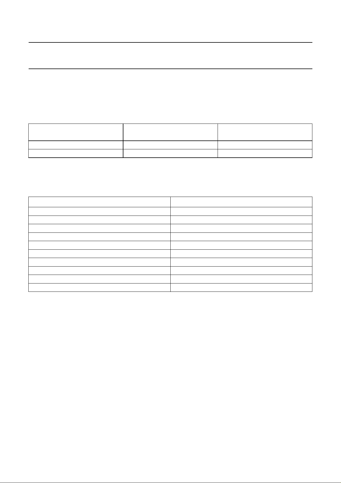
Module Maker programmable parameters are stored in 10 non-volatile cells.
Table 14 Non-volatile cell list
CELL[9:0] DESCRIPTION
9V
8V
7V
6V
5V
4MF
3 BS100
2 TC1[1]
1 TC1[0]
0SB
MODULE MAKER
PROGRAMMABLE PARAMETERS
[4]
CAL
[3]
CAL
[2]
CAL
[1]
CAL
[0]
CAL
An unprogrammed cell contains 0. A programmed cell contains 1. OM6213 dice are shipped to the Module Maker with
all cells unprogrammed (containing 0). An unprogrammed cell may be programmed by using the described procedure.
A programmed cell cannot be unprogrammed to 0.
2001 Nov 07 26
Page 27
Philips Semiconductors Product specification
48 × 84 pixels matrix LCD driver OM6213
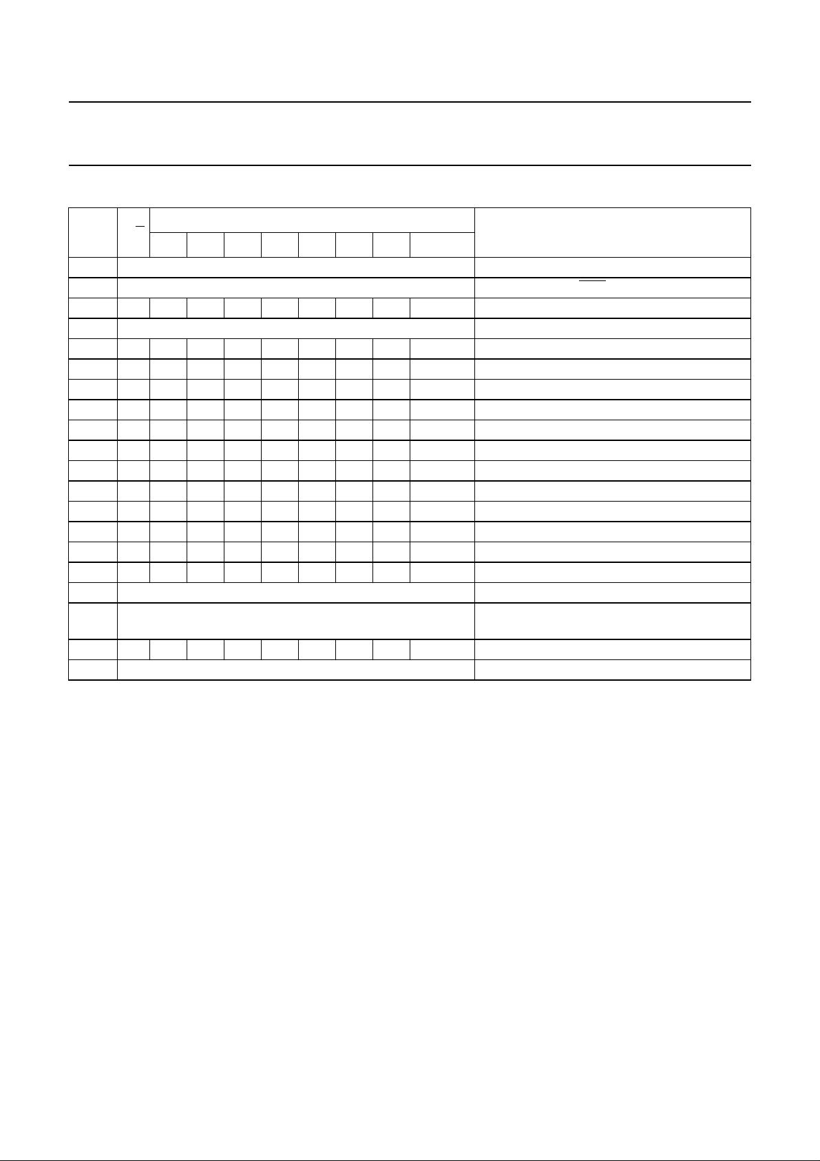
Table 15 Module Maker parameters programming procedure
STEP D/C
ACTION
DB7 DB6 DB5 DB4 DB3 DB2 DB1 DB0
1 switch power on
2 reset the device (RES pulse)
3 0 0 0 1 0 0 0 0 0 exit Power-down and set H = 0 instruction set
4 wait 5 ms
5 0 0 0 1 0 0 1 0 0 enter Power-down
6 0 0 0 0 0 0 1 0 1 enter programming mode
COMMAND BYTE
7 0 1 0 0 0 0 0 0 CELL[9] specify CELL[9] (V
8 0 1 0 0 0 0 0 0 CELL[8] specify CELL[8] (V
9 0 1 0 0 0 0 0 0 CELL[7] specify CELL[7] (V
10 0 1 0 0 0 0 0 0 CELL[6] specify CELL[6] (V
11 0 1 0 0 0 0 0 0 CELL[5] specify CELL[5] (V
CAL
CAL
CAL
CAL
CAL
[4])
[3])
[2])
[1])
[0])
12 0 1 0 0 0 0 0 0 CELL[4] specify CELL[4] (MF)
13 0 1 0 0 0 0 0 0 CELL[3] specify CELL[3] (BS100)
14 0 1 0 0 0 0 0 0 CELL[2] specify CELL[2] (TC1[1])
15 0 1 0 0 0 0 0 0 CELL[1] specify CELL[1] (TC1[0])
16 0 1 0 0 0 0 0 0 CELL[0] specify CELL[0] (SB)
17 apply programming waveforms
18 go back to step 7 if other cells need to be
programmed (see note 5)
19 0 0 0 0 0 0 0 0 0 exit programming mode
20 switch power off
Notes
1. Programming voltages are applied via pins SDIN and VLCDIN.
2. It is possible to program only one cell at a time. When applying programming waveforms, all cells (except the one
being programmed) should be 0; see also example in note 5.
3. The seal bit (SB) must be the last to be programmed, since no further programming is possible when SB = 1.
4. Ifthe seal bit is unprogrammed (SB = 0) thedefaults (andnot the Module Maker programmed parameters) are taken
into account.
5. Example:a device has to be programmed to use a charge pump with a multiplication factor equal to 3 (initial state is
MF = SB = 0, final state is MF = SB = 1).
a) Execute steps 1 to 6.
b) Set CELL[9:0] to 0000010000 (steps 7 to 16).
c) Apply programming waveforms (step 17): MF cell is now programmed (MF = 1, SB = 0).
d) Go back to step 7.
e) Set CELL[9:0] to 0000000001 (steps 7 to 16).
f) Apply programming waveforms (step 17): SB cell is now programmed (MF = SB = 1).
g) Execute steps 18 to 20.
6. Programming waveforms MUST only be applied at step 17.
2001 Nov 07 27
Page 28

Philips Semiconductors Product specification
48 × 84 pixels matrix LCD driver OM6213
Table 16 Programming parameters
SYMBOL PARAMETER CONDITION MIN. TYP. MAX. UNIT
V
SDIN
V
LCDIN
I
LCDIN
I
SDIN
T
amb(prog)
t
su;SCLK
t
h;SCLK
t
su;SDIN
t
h;SDIN
t
W
voltage applied to pin SDIN relative
to V
SS1
voltage applied to pin V
relative to V
SS1
current drawn by V
LCDIN
LCDIN
during
programming
current drawn by V
SDIN
during
programming
ambient temperature during
programming
set-up of internal data after last
clock
hold of internal data before next
clock
set-up of V
SDIN
prior to
programming
hold of V
after programming 1 − 10 ms
SDIN
pulse width of programming voltage 100 120 200 ms
notes 1 and 3
programming active 11 11.5 12 V
programming
0 − V
DD1
inactive
notes 1 and 2
programming active 9 9.5 10 V
programming
0 − V
DD2
inactive
when programming a
− 850 1000 µA
single bit to one
− 100 200 µA
02540
1 −−µs
1 −−µs
1 − 10 ms
V
V
o
C
Notes
1. The voltage drop across the ITO track and zebra connector must be taken into account to guarantee sufficient
voltage at the chip pins.
2. The high voltage generator must be disabled (VPR= 0) when the V
pin is being driven.
LCDIN
3. Maximum voltage must never be exceeded (even for a short time). Care must be taken when applying the
programming waveforms in order to avoid overshoots.
2001 Nov 07 28
Page 29
Philips Semiconductors Product specification
48 × 84 pixels matrix LCD driver OM6213
handbook, full pagewidth
SCLK
SDIN
V
LCDIN
DB1
DB0 DB7 DB6
t
su;SCLK
t
su;SDIN
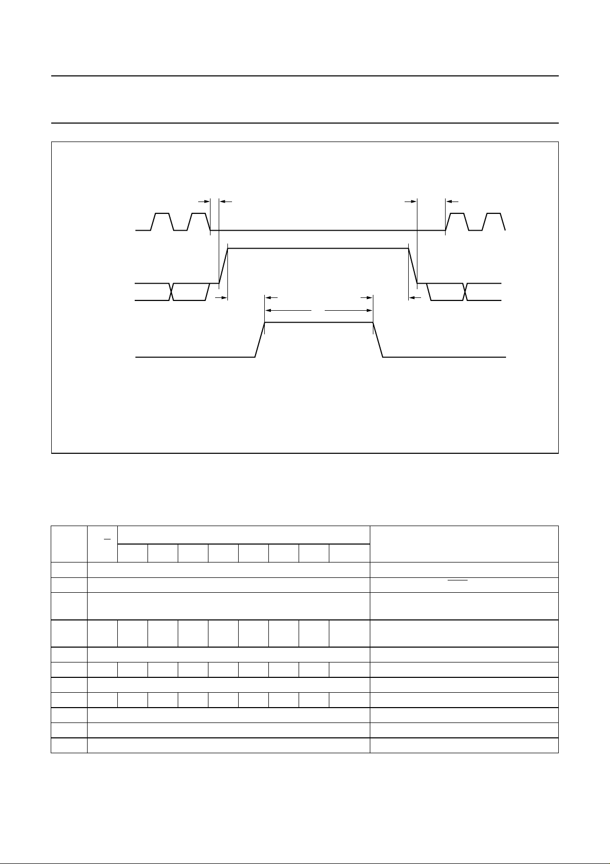
Fig.19 Programming waveforms.
20.7 Example of V
calibration flow
LCD
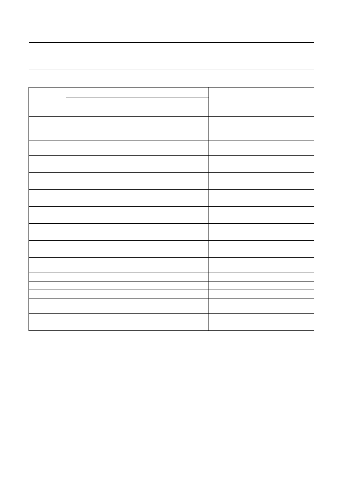
The following tables are examples of the flow to calibrate V
LCD
t
h;SCLK
t
h;SDIN
t
W
MGT853
.
Table 17 V
calibration flow 1
LCD
COMMAND BYTE
STEP D/
C
ACTION
DB7 DB6 DB5 DB4 DB3 DB2 DB1 DB0
1 switch power on
2 reset the device (
RES pulse)
3 configure the device and fill in the DDRAM
without switching the charge pump on
4 000100001 exit Power-down and set H = 1 instruction
set
5 wait 5 ms
6 01V
PR6VPR5VPR4VPR3VPR2VPR1VPR0
7 measure V
set VPR and switch charge pump on
LCD
8 010000000 switch charge pump off
9 switch power off
10 calculate V
11 store V
[4:0] with look-up tables
CAL
[4:0] for programming later
CAL
2001 Nov 07 29
Page 30
Philips Semiconductors Product specification
48 × 84 pixels matrix LCD driver OM6213
Table 18 V
calibration flow 2
LCD
COMMAND BYTE
STEP D/
C
ACTION
DB7 DB6 DB5 DB4 DB3 DB2 DB1 DB0
1 switch power on
2 reset the device (RES pulse)
3 configure the deviceand fill in the DDRAM
without switching the charge pump on
4 00010000 0exitPower-down and set H = 0 instruction
set
5 wait 5 ms
6 00000010 1enter programming mode
7 01000000CELL[9] specify CELL[9] (V
8 01000000CELL[8] specify CELL[8] (V
9 01000000CELL[7] specify CELL[7] (V
10 01000000CELL[6] specify CELL[6] (V
11 01000000CELL[5] specify CELL[5] (V
CAL
CAL
CAL
CAL
CAL
[4])
[3])
[2])
[1])
[0])
12 01000000CELL[4] specify CELL[4] (MF)
13 01000000CELL[3] specify CELL[3] (BS100)
14 01000000CELL[2] specify CELL[2] (TC1[1])
15 01000000CELL[1] specify CELL[1] (TC1[0])
16 00000000 1specify CELL[0] = 1 (SB = 1)
17 00010000 1set H = 1 instruction set (exit
programming mode)
18 0 1 V
PR6VPR5VPR4VPR3VPR2VPR1
19 measure V
V
set VPR and switch charge pump on
PR0
LCD
20 01000000 0switch charge pump off
21 if V
is not correct, go back to step 2
LCD
and try a different V
CAL
[4:0]
22 switch power off
23 store V
[4:0] for programming later
CAL
2001 Nov 07 30
Page 31
Philips Semiconductors Product specification
48 × 84 pixels matrix LCD driver OM6213
21 CHIP INFORMATION
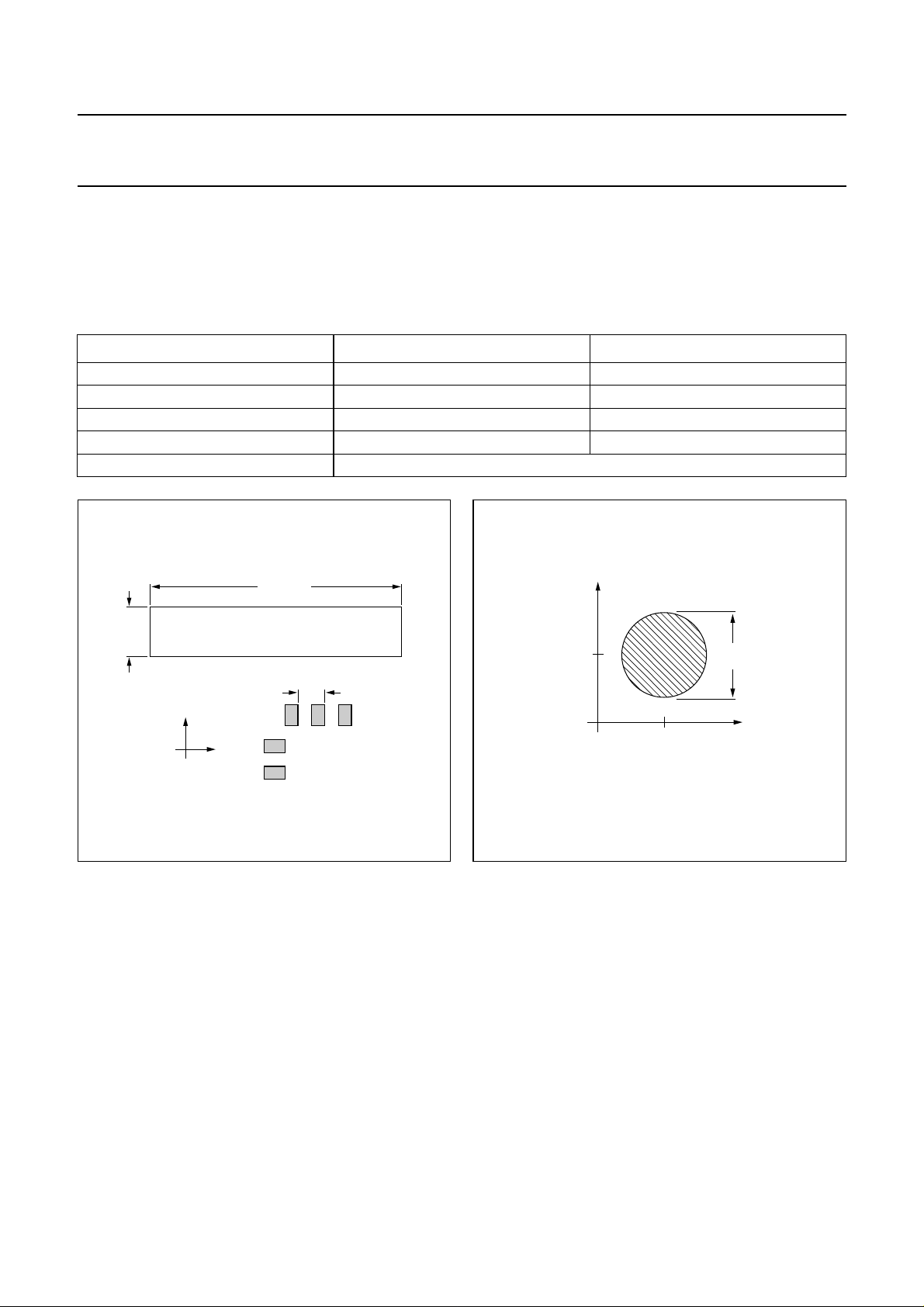
The OM6213 is manufactured in n-well CMOS technology.
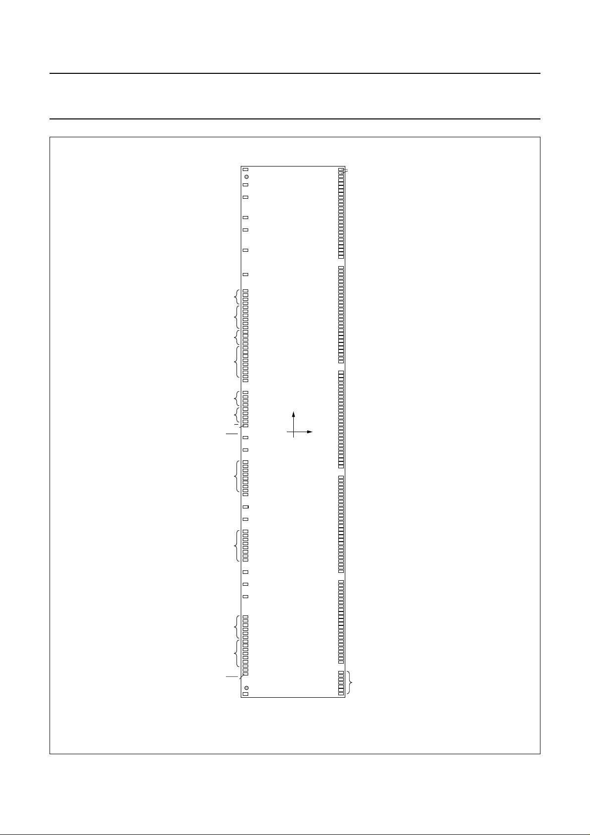
22 BONDING PAD INFORMATION
Table 19 Bonding pad information
NAME ROW/COL SIDE INTERFACE SIDE
Pad pitch 60 µm (min.) 70 µm (min.)
Pad size, aluminium 50 × 90 µm (min.) 60× 100 µm (min.)
CBB opening 26 × 66 µm (min.) 36 × 76 µm (min.)
Bump dimensions 40 × 80 × 17.5 µm (±5) (min.) 50 × 90 × 17.5 µm (±5) (min.)
Wafer thickness (excluding bumps) 381 µm (±25)
handbook, halfpage
1.78
mm
9.11 mm
OM6213
y
x
Fig.20 Bonding pads.
pitch
MGT854
handbook, halfpage
y center
x center
MGT855
Fig.21 Shape of alignment mark (100 µm
diameter).
100
µm
2001 Nov 07 31
Page 32
Philips Semiconductors Product specification
48 × 84 pixels matrix LCD driver OM6213
23 BONDING PAD LOCATION
Table 20 Bonding pad location
All x and y co-ordinates are referenced to the centre of
the chip (dimensions in µm; seeFig.22).
COORDINATES
SYMBOL PAD
xy
Dummy pad 1 −820 +4505
Alignment 2 −810 +4385
V
V
V
V
V
OS4
OS3
OS2
OS1
OS0
3 −820 +4240
4 −820 +4030
5 −820 +3680
6 −820 +3470
7 −820 +3120
Dummy pad 8 −820 +2700
Dummy pad 9 −820 +2420
Dummy pad 10 −820 +2350
Dummy pad 11 −820 +2280
Dummy pad 12 −820 +2210
V
V
V
V
V
V
V
V
V
V
V
V
V
V
V
V
V
V
DD1
DD1
DD1
DD1
DD1
DD1
DD3
DD3
DD3
DD3
DD2
DD2
DD2
DD2
DD2
DD2
DD2
DD2
13 −820 +2140
14 −820 +2070
15 −820 +2000
16 −820 +1930
17 −820 +1860
18 −820 +1790
19 −820 +1720
20 −820 +1650
21 −820 +1580
22 −820 +1510
23 −820 +1440
24 −820 +1370
25 −820 +1300
26 −820 +1230
27 −820 +1160
28 −820 +1090
29 −820 +1020
30 −820 +950
SCLK 31 −820 +880
T7 32 −820 +670
T7 33 −820 +600
T7 34 −820 +530
T7 35 −820 +460
SDIN 36 −820 +390
SYMBOL PAD
COORDINATES
xy
SDIN 37 −820 +320
SDIN 38 −820 +250
SDIN 39 −820 +180
D/
C40−820 +110
SCE 41 −820 −100
OSC 42 −820 −310
V
SS2
V
SS2
V
SS2
V
SS2
V
SS2
V
SS2
V
SS2
V
SS2
43 −820 −520
44 −820 −590
45 −820 −660
46 −820 −730
47 −820 −800
48 −820 −870
49 −820 −940
50 −820 −1010
T4 51 −820 −1080
T5 52 −820 −1290
T6 53 −820 −1500
V
SS1
V
SS1
V
SS1
V
SS1
V
SS1
V
SS1
V
SS1
V
SS1
54 −820 −1710
55 −820 −1780
56 −820 −1850
57 −820 −1920
58 −820 −1990
59 −820 −2060
60 −820 −2130
61 −820 −2200
T1 62 −820 −2410
T2 63 −820 −2620
T3 64 −820 −2830
V
LCDIN
V
LCDIN
V
LCDIN
V
LCDIN
V
LCDIN
V
LCDIN
V
LCDOUT
V
LCDOUT
V
LCDOUT
V
LCDOUT
V
LCDOUT
65 −820 −3180
66 −820 −3250
67 −820 −3320
68 −820 −3390
69 −820 −3460
70 −820 −3530
71 −820 −3600
72 −820 −3670
73 −820 −3740
74 −820 −3810
75 −820 −3880
2001 Nov 07 32
Page 33
Philips Semiconductors Product specification
48 × 84 pixels matrix LCD driver OM6213
SYMBOL PAD
V
LCDOUT
V
LCDOUT
VLCDSEN 78 −820 −4090
RES 79 −820 −4160
Alignment 80 −810 −4400
Dummy pad 81 −820 −4505
Dummy pad 82 +825 −4495
Dummy pad 83 +825 −4435
Dummy pad 84 +825 −4375
Dummy pad 85 +825 −4315
Dummy pad 86 +825 −4255
Dummy pad 87 +825 −4195
Dummy pad 88 +825 −4135
ROW 11 89 +825 −3955
ROW 10 90 +825 −3895
ROW 9 91 +825 −3835
ROW 8 92 +825 −3775
ROW 7 93 +825 −3715
ROW 6 94 +825 −3655
ROW 5 95 +825 −3595
ROW 4 96 +825 −3535
ROW 3 97 +825 −3475
ROW 2 98 +825 −3415
ROW 1 99 +825 −3355
ROW 0 100 +825 −3295
ROW 12 101 +825 −3235
ROW 13 102 +825 −3175
ROW 14 103 +825 −3115
ROW 15 104 +825 −3055
ROW 16 105 +825 −2995
ROW 17 106 +825 −2935
ROW 18 107 +825 −2875
ROW 19 108 +825 −2815
ROW 20 109 +825 −2755
ROW 21 110 +825 −2695
ROW 22 111 +825 −2635
ROW 23 112 +825 −2575
COL 0 113 +825 −2395
COL 1 114 +825 −2335
76 −820 −3950
77 −820 −4020
COORDINATES
xy
SYMBOL PAD
COORDINATES
xy
COL 2 115 +825 −2275
COL 3 116 +825 −2215
COL 4 117 +825 −2155
COL 5 118 +825 −2095
COL 6 119 +825 −2035
COL 7 120 +825 −1975
COL 8 121 +825 −1915
COL 9 122 +825 −1855
COL 10 123 +825 −1795
COL 11 124 +825 −1735
COL 12 125 +825 −1675
COL 13 126 +825 −1615
COL 14 127 +825 −1555
COL 15 128 +825 −1495
COL 16 129 +825 −1435
COL 17 130 +825 −1375
COL 18 131 +825 −1315
COL 19 132 +825 −1255
COL 20 133 +825 −1195
COL 21 134 +825 −1135
COL 22 135 +825 −1075
COL 23 136 +825 −1015
COL 24 137 +825 −955
COL 25 138 +825 −895
COL 26 139 +825 −835
COL 27 140 +825 −775
COL 28 141 +825 −595
COL 29 142 +825 −535
COL 30 143 +825 −475
COL 31 144 +825 −415
COL 32 145 +825 −355
COL 33 146 +825 −295
COL 34 147 +825 −235
COL 35 148 +825 −175
COL 36 149 +825 −115
COL 37 150 +825 −55
COL 38 151 +825 +5
COL 39 152 +825 +65
COL 40 153 +825 +125
2001 Nov 07 33
Page 34
Philips Semiconductors Product specification
48 × 84 pixels matrix LCD driver OM6213
SYMBOL PAD
COORDINATES
xy
COL 41 154 +825 +185
COL 42 155 +825 +245
COL 43 156 +825 +305
COL 44 157 +825 +365
COL 45 158 +825 +425
COL 46 159 +825 +485
COL 47 160 +825 +545
COL 48 161 +825 +605
COL 49 162 +825 +665
COL 50 163 +825 +725
COL 51 164 +825 +785
COL 52 165 +825 +845
COL 53 166 +825 +905
COL 54 167 +825 +965
COL 55 168 +825 +1025
COL 56 169 +825 +1205
COL 57 170 +825 +1265
COL 58 171 +825 +1325
COL 59 172 +825 +1385
COL 60 173 +825 +1445
COL 61 174 +825 +1505
COL 62 175 +825 +1565
COL 63 176 +825 +1625
COL 64 177 +825 +1685
COL 65 178 +825 +1745
COL 66 179 +825 +1805
COL 67 180 +825 +1865
COL 68 181 +825 +1925
COL 69 182 +825 +1985
COL 70 183 +825 +2045
COL 71 184 +825 +2105
COL 72 185 +825 +2165
COL 73 186 +825 +2225
COL 74 187 +825 +2285
COL 75 188 +825 +2345
SYMBOL PAD
COORDINATES
xy
COL 76 189 +825 +2405
COL 77 190 +825 +2465
COL 78 191 +825 +2525
COL 79 192 +825 +2585
COL 80 193 +825 +2645
COL 81 194 +825 +2705
COL 82 195 +825 +2765
COL 83 196 +825 +2825
ROW 47 197 +825 +3005
ROW 46 198 +825 +3065
ROW 45 199 +825 +3125
ROW 44 200 +825 +3185
ROW 43 201 +825 +3245
ROW 42 202 +825 +3305
ROW 41 203 +825 +3365
ROW 40 204 +825 +3425
ROW 39 205 +825 +3485
ROW 38 206 +825 +3545
ROW 37 207 +825 +3605
ROW 36 208 +825 +3665
ROW 24 209 +825 +3725
ROW 25 210 +825 +3785
ROW 26 211 +825 +3845
ROW 27 212 +825 +3905
ROW 28 213 +825 +3965
ROW 29 214 +825 +4025
ROW 30 215 +825 +4085
ROW 31 216 +825 +4145
ROW 32 217 +825 +4205
ROW 33 218 +825 +4265
ROW 34 219 +825 +4325
ROW 35 220 +825 +4385
Dummy pad 221 +825 +4445
Dummy pad 222 +825 +4505
2001 Nov 07 34
Page 35
Philips Semiconductors Product specification
48 × 84 pixels matrix LCD driver OM6213
dummy pad dummy pad
V
dummy pad
dummy pad
V
DD1
V
DD3
V
DD2
SDIN
V
SS2
OS4
V
OS3
V
OS2
V
OS1
V
OS0
SCLK
T7
D/C
SCE
OSC
T4
T5
T6
alignment mark
y
0,0
ROW 35
.
.
.
.
.
.
ROW 24
ROW 36
.
.
.
.
.
.
ROW 47
COL 83
.
.
.
.
.
.
COL 56
COL 55
.
.
.
x
.
.
.
COL 28
COL 27
.
.
.
V
SS1
T1
T2
T3
V
LCDIN
V
LCDOUT
V
LCDSEN
RES
dummy pad
alignment mark
Fig.22 Pad locations.
2001 Nov 07 35
OM6213
MGT856
.
.
.
COL 0
ROW 23
.
.
.
.
.
.
ROW 12
ROW 0
.
.
.
.
.
.
ROW 11
dummy pad
Page 36
Philips Semiconductors Product specification
48 × 84 pixels matrix LCD driver OM6213
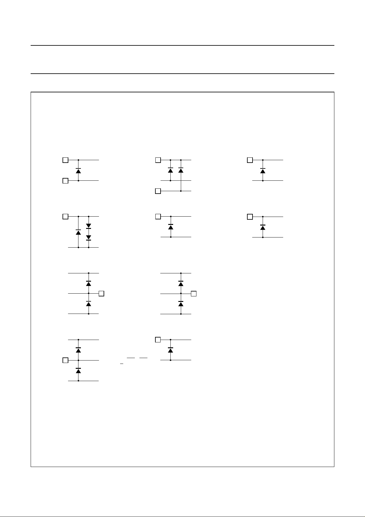
24 DEVICE PROTECTION DIAGRAM
handbook, full pagewidth
V
DD1
V
SS1
V
SS2
V
SS1
V
DD1
T1, T2, T3, T6
V
SS1
V
DD2
V
SS1
V
SS2
V
LCDIN
V
LCDSENSE
V
SS1
V
LCDIN
V
SS1
V
DD3
V
SS1
,
V
LCDOUT
V
SS1
V
DD1
OSC, SCLK, SCE, RES,
T4, T5, D/C, V
V
SS1
The conditions for continuity test are as follows:
Maximum forward current = 5 mA; Maximum reverse voltage = 5 V.
OS
[
]
4:0
Fig.23 Device protection diagram.
2001 Nov 07 36
SDIN, T7
V
SS1
MGT858
Page 37
Philips Semiconductors Product specification
48 × 84 pixels matrix LCD driver OM6213
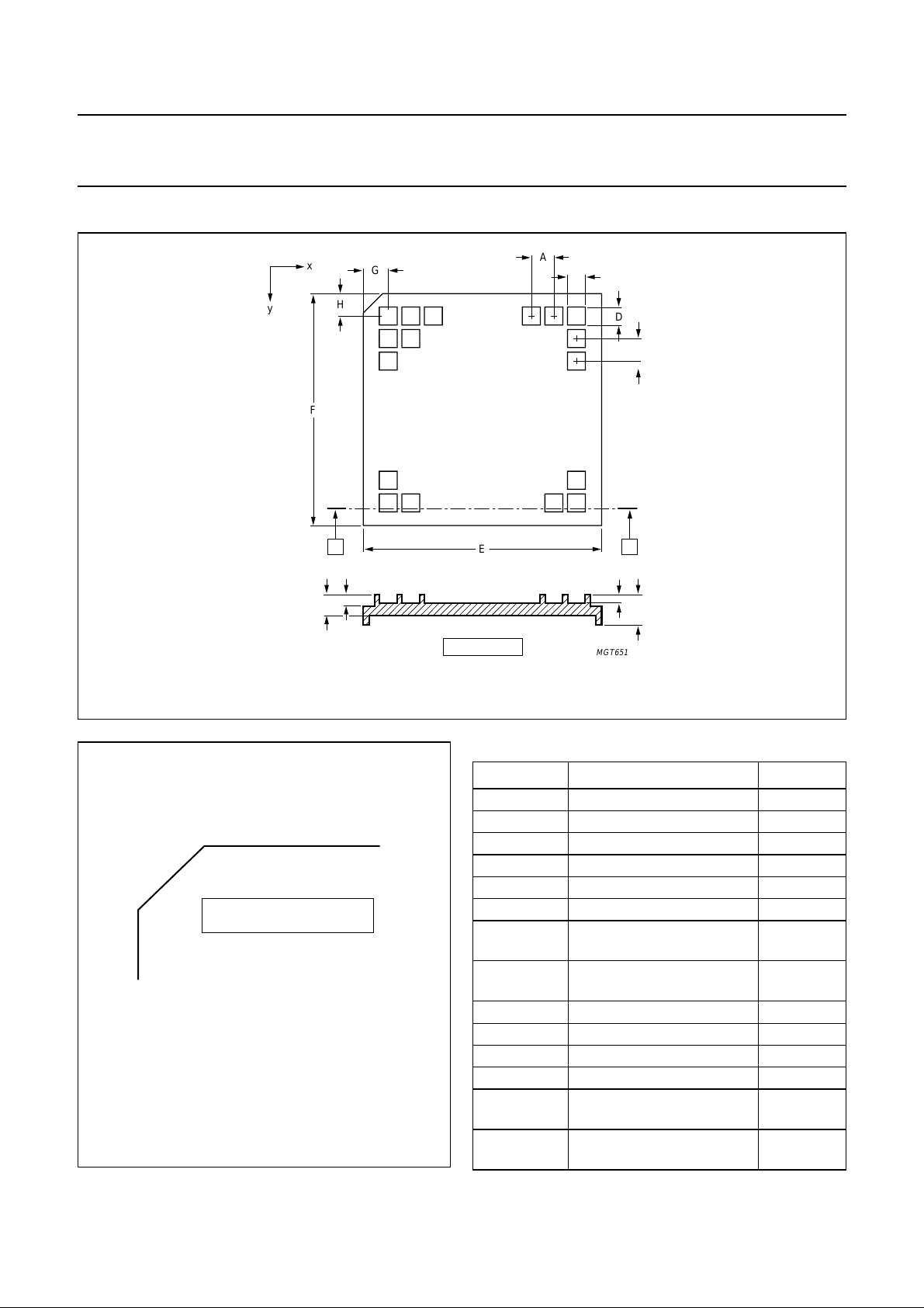
25 TRAY INFORMATION
handbook, full pagewidth
x
y
F
L
G
H
1,1 x,12,1
3,1
1,2
2,2
1,3
1,y
A
K
E
SECTION A-A
A
C
D
B
x,y
A
M
J
MGT651
Fig.24 Tray details.
handbook, halfpage
OM6213-1
MGT857
The orientationof the IC in a pocketis indicated by the position ofthe
IC type name on the die surface with respect to the chamfer on the
upper left corner of the tray. Refer to the bonding pad location
diagram for the orientating and position of the type name on the
surface.
Fig.25 Tray alignment.
Table 21 Tray dimensions
DIMENSION DESCRIPTION VALUE
A pocket pitch, x direction 14.45 mm
B pocket pitch, y direction 3.76 mm
C pocket width, x direction 9.31 mm
D pocket width, y direction 1.98 mm
E tray width, x direction 50.8 mm
F tray width, y direction 50.8 mm
G distance from cut corner to
10.95 mm
pocket (1 and 1) centre
H distance from cut corner to
4.72 mm
pocket (1 and 1) centre
J tray thickness 3.96 mm
K tray cross section 1.78 mm
L tray cross section 2.44 mm
M pocket depth 0.89 mm
x number of pockets in
3
x direction
y number of pockets in
12
y direction
2001 Nov 07 37
Page 38

Philips Semiconductors Product specification
48 × 84 pixels matrix LCD driver OM6213
26 DATA SHEET STATUS
PRODUCT
DATA SHEET STATUS
Objective data Development This data sheet contains data from the objective specification for product
Preliminary data Qualification This data sheet contains data from the preliminary specification.
Product data Production This data sheet contains data from the product specification. Philips
(1)
STATUS
(2)
DEFINITIONS
development. Philips Semiconductors reserves the right to change the
specification in any manner without notice.
Supplementary data will be published at a later date. Philips
Semiconductors reserves the right to change the specification without
notice, in order to improve the design and supply the best possible
product.
Semiconductors reserves the right to make changes at any time in order
to improve the design, manufacturing and supply. Changes will be
communicated according to the Customer Product/Process Change
Notification (CPCN) procedure SNW-SQ-650A.
Notes
1. Please consult the most recently issued data sheet before initiating or completing a design.
2. The product status of the device(s) described in this data sheet may have changed since this data sheet was
published. The latest information is available on the Internet at URL http://www.semiconductors.philips.com.
27 DEFINITIONS
Short-form specification The data in a short-form
specification is extracted from a full data sheet with the
same type number and title. For detailed information see
the relevant data sheet or data handbook.
Limiting values definition Limiting values given are in
accordance with the Absolute Maximum Rating System
(IEC 60134). Stress above one or more of the limiting
values may cause permanent damage to the device.
These are stress ratings only and operation of the device
atthese or at anyotherconditionsabove those given inthe
Characteristics sections of the specification is not implied.
Exposure to limiting values for extended periods may
affect device reliability.
Application information Applications that are
described herein for any of these products are for
illustrative purposes only. Philips Semiconductors make
norepresentationorwarranty that such applications willbe
suitable for the specified use without further testing or
modification.
28 DISCLAIMERS
Life support applications These products are not
designed for use in life support appliances, devices, or
systems where malfunction of these products can
reasonably be expected to result inpersonal injury. Philips
Semiconductorscustomersusingor selling these products
for use in such applications do so at their own risk and
agree to fully indemnify Philips Semiconductors for any
damages resulting from such application.
Right to make changes Philips Semiconductors
reserves the right to make changes, without notice, in the
products, including circuits, standard cells, and/or
software, described or contained herein in order to
improve design and/or performance. Philips
Semiconductors assumes no responsibility or liability for
theuseof any of these products,conveysnolicence or title
under any patent, copyright, or mask work right to these
products,and makes no representationsorwarranties that
these products are free from patent, copyright, or mask
work right infringement, unless otherwise specified.
2001 Nov 07 38
Page 39

Philips Semiconductors Product specification
48 × 84 pixels matrix LCD driver OM6213
NOTES
2001 Nov 07 39
Page 40

Philips Semiconductors – a w orldwide compan y
Contact information
For additional information please visit http://www.semiconductors.philips.com. Fax: +31 40 27 24825
For sales offices addresses send e-mail to: [email protected].
© Koninklijke Philips Electronics N.V. 2001
All rights are reserved. Reproduction in whole or in part is prohibited without the prior written consent of the copyright owner.
The information presented in this document does not form part of any quotation or contract, is believed to be accurate and reliable and may be changed
without notice. No liability will be accepted by the publisher for any consequence of its use. Publication thereof does not convey nor imply any license
under patent- or other industrial or intellectual property rights.
Printed in The Netherlands 403506/01/pp40 Date of release: 2001 Nov 07 Document order number: 9397 750 07745
SCA73
 Loading...