

Page 1

查询AU5517D供应商查询AU5517D供应商
INTEGRATED CIRCUITS
NE5517/NE5517A/AU5517
Dual operational transconductance
amplifier
Product data
Replaces NE5517/NE5517A dated 2001 Aug 03
2002 Dec 06
Page 2
Philips Semiconductor Product data
Dual operational transconductance amplifier
DESCRIPTION
The AU5517 and NE5517 contain two current-controlled
transconductance amplifiers, each with a differential input and
push-pull output. The AU5517/NE5517 offers significant design and
performance advantages over similar devices for all types of
programmable gain applications. Circuit performance is enhanced
through the use of linearizing diodes at the inputs which enable a
10 dB signal-to-noise improvement referenced to 0.5% THD. The
AU5517/NE5517 is suited for a wide variety of industrial and
consumer applications.
Constant impedance buffers on the chip allow general use of the
AU5517/NE5517. These buffers are made of Darlington transistors
and a biasing network that virtually eliminate the change of offset
voltage due to a burst in the bias current I
, hence eliminating the
ABC
audible noise that could otherwise be heard in high quality audio
applications.
FEA TURES
•Constant impedance buffers
•∆V
of buffer is constant with amplifier I
BE
BIAS
change
•Excellent matching between amplifiers
•Linearizing diodes
•High output signal-to-noise ratio
APPLICA TIONS
•Multiplexers
•Timers
•Electronic music synthesizers
•Dolby HX Systems
•Current-controlled amplifiers, filters
•Current-controlled oscillators, impedances
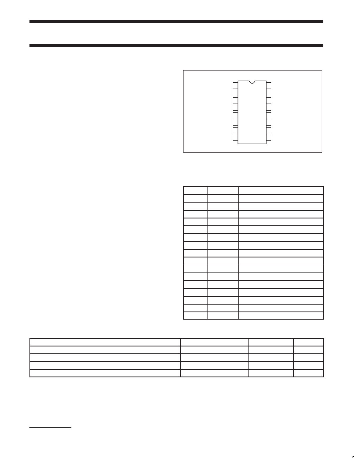
PIN CONFIGURATION
PIN DESIGNA TION
PIN NO. SYMBOL NAME AND FUNCTION
NE5517/NE5517A/
N, D Packages
1
I
ABCa
2
D
a
3
+IN
a
4
–IN
a
5
VO
a
6
V–
INBUFFER
VO
BUFFERa
1 I
2 D
3 +IN
4 –IN
5 V
6 V– Negative supply
7 IN
BUFFERa
8 VO
9 VO
10 IN
BUFFERb
11 V+ Positive supply
12 V
13 –IN
14 +IN
15 D
16 I
7
a
8
Top View
Figure 1. Pin Configuration
ABCa
Oa
Amplifier bias input A
Diode bias A
a
Non-inverting input A
a
Inverting input A
a
Output A
Buffer input A
BUFFERa
BUFFERb
Buffer output A
Buffer output B
Buffer input B
Ob
ABCb
Output B
Inverting input B
b
Non-inverting input B
b
Diode bias B
b
Amplifier bias input B
16
15
14
13
12
11
10
9
I
ABCb
D
b
+IN
b
–IN
b
VO
b
V+
IN
BUFFERb
VO
BUFFERb
SL00306
AU5517
ORDERING INFORMATION
DESCRIPTION TEMPERATURE RANGE ORDER CODE DWG #
16-Pin Plastic Dual In-Line Package (DIP) 0 to +70 °C NE5517N SOT38-4
16-Pin Plastic Dual In-Line Package (DIP) 0 to +70 °C NE5517AN SOT38-4
16-Pin Small Outline (SO) Package 0 to +70 °C NE5517D SOT109-1
16-Pin Small Outline (SO) Package –40 to +125 °C AU5517D SOT109-1
Dolby is a registered trademark of Dolby Laboratories Inc., San Francisco, Calif.
2002 Dec 06
2
Page 3
Philips Semiconductor Product data
Dual operational transconductance amplifier
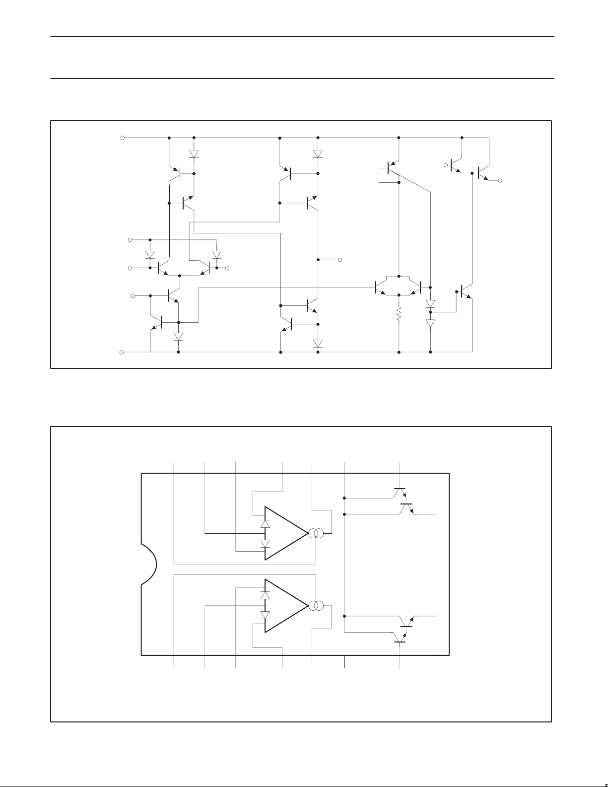
CIRCUIT SCHEMATIC
V+
11
D4
2,15
–INPUT
AMP BIAS
INPUT
V–
6
4,13
1,16
Q6
Q7
D2
Q4
Q5
Q2
Q1
D1
D3
+INPUT
3,14
Q10
Q8
Figure 2. Circuit Schematic
Q9
Q11
NE5517/NE5517A/
AU5517
D6
Q14
V
OUTPUT
5,12
Q15 Q16
R1
D5
7,10
D7
D8
Q12
Q13
8,9
Q3
SL00307
CONNECTION DIAGRAM
B
AMP
BIAS
INPUT
16 15 14 13 12 11 10 9
INPUT
NOTE:
1. V+ of output buffers and amplifiers are internally connected.
DIODE
123 45 6 7 8
AMP
DIODE
BIAS
A
B
BIAS
BIAS
AA
B
INPUT
(+)
INPUT
(+)
Figure 3. Connection Diagram
INPUT
–
+
+
–
INPUT
B
(–)
(–)
A
B
OUTPUT
B
A
OUTPUT
V+ (1)
A
V–
B
BUFFER
INPUT
BUFFER
INPUT
A
B
BUFFER
OUTPUT
BUFFER
OUTPUT
A
SL00308
2002 Dec 06
3
Page 4
Philips Semiconductor Product data
Dual operational transconductance amplifier
NE5517/NE5517A/
AU5517
ABSOLUTE MAXIMUM RATINGS
SYMBOL PARAMETER RATING UNIT
V
S
P
D
Supply voltage
Power dissipation,
T
= 25 °C (still air)
amb
NE5517N, NE5517AN 1500 mW
NE5517D, AU5517D 1125 mW
V
I
D
I
ABC
I
SC
I
OUT
T
IN
amb
Differential input voltage ±5 V
Diode bias current 2 mA
Amplifier bias current 2 mA
Output short-circuit duration Indefinite
Buffer output current
Operating temperature range
NE5517N, NE5517AN 0 °C to +70 °C °C
AU5517D –40 °C to +125 °C °C
V
DC
T
stg
T
sld
DC input voltage +VS to –V
Storage temperature range –65 °C to +150 °C °C
Lead soldering temperature (10 sec max) 230 °C
NOTES:
1. For selections to a supply voltage above ±22 V, contact factory
2. The following derating factors should be applied above 25 °C
N package at 12.0 mW/°C
D package at 9.0 mW/°C
3. Buffer output current should be limited so as to not exceed package dissipation.
1
2
3
44 VDC or ±22 V
20 mA
S
2002 Dec 06
4
Page 5
Philips Semiconductor Product data
SYMBOL
PARAMETER
TEST CONDITIONS
UNIT
I
BIAS
In ut bias current
gMForward transconductance
Dual operational transconductance amplifier
NE5517/NE5517A/
AU5517
DC ELECTRICAL CHARACTERISTICS
V
OS
V
OS
I
OS
I
OUT
V
OUT
I
CC
CMRR
I
IN
R
IN
B
W
SR Slew rate Unity gain compensated 50 50 V/µs
IN
BUFFER
VO
BUFFER
NOTES:
1. These specifications apply for V
specified. The inputs to the buffers are grounded and outputs are open.
2. These specifications apply for V
connected to the transconductance amplifier output.
= ±15, R
3. V
S
Input offset voltage Over temperature range 5 mV
∆VOS/∆T Avg. TC of input offset voltage 7 7 µV/°C
VOS including diodes Diode bias current (ID) = 500 µA 0.5 5 0.5 2 mV
Input offset change 5 µA ≤ I
Input offset current 0.1 0.6 0.1 0.6 µA
∆IOS/∆T Avg. TC of input offset current 0.001 0.001 µA/°C
p
∆IB/∆T Avg. TC of input current 0.01 0.01 µA/°C
gM tracking 0.3 0.3 dB
Peak output current RL = 0, I
Peak output voltage
Positive RL = ∞, 5 µA ≤ I
Negative RL = ∞, 5 µA ≤ I
Supply current I
VOS sensitivity
Positive ∆ VOS/∆ V+ 20 150 20 150 µV/V
Negative ∆ VOS/∆ V– 20 150 20 150 µV/V
Common-mode rejection
ration
Common-mode range ±12 ±13.5 ±12 ±13.5 V
Crosstalk
Differential input current I
Leakage current I
Input resistance 10 26 10 26 kΩ
Open-loop bandwidth 2 2 MHz
Buffer input current 5 0.4 5 0.4 5 µA
Peak buffer output voltage 5 10 10 V
∆VBE of buffer Refer to Buffer VBE test circuit
= ±15 V, T
S
= ±15 V, I
S
= 5 kΩ connected from Buffer output to –VS and 5 µA ≤ I
OUT
1
AU5517/NE5517 NE5517A
Min Typ Max Min Typ Max
0.4 5 0.4 2 mV
I
5 µA 0.3 5 0.3 2 mV
ABC
≤ 500 µA 0.1 0.1 3 mV
ABC
0.4 5 0.4 5 µA
Over temperature range 1 8 1 7 µA
6700 9600 1300 7700 9600 1200 µmho
Over temperature range 5400 4000 µmho
RL = 0, I
=5 µA 5 3 5 7 µA
ABC
= 500 µA 350 500 650 350 500 650 µA
ABC
RL = 0 300 300 µA
≤ 500 µA +12 +14.2 +12 +14.2 V
ABC
≤ 500 µA –12 –14.4 –12 –14.4 V
ABC
= 500 µA, both channels 2.6 4 2.6 4 mA
ABC
80 110 80 110 dB
Referred to input2
20 Hz < f < 20 kHz
= 0, input = ±4 V 0.02 100 0.02 10 nA
ABC
= 0 (Refer to test circuit) 0.2 100 0.2 5 nA
ABC
3
= 25 °C, amplifier bias current (I
amb
= 500 µA, R
ABC
= 5 kΩ connected from the buffer output to –VS and the input of the buffer is
OUT
≤ 500 µA.
ABC
100 100 dB
0.5 5 0.5 5 mV
) = 500 µA, Pins 2 and 15 open unless otherwise
ABC
2002 Dec 06
5
Page 6
Philips Semiconductor Product data
Dual operational transconductance amplifier
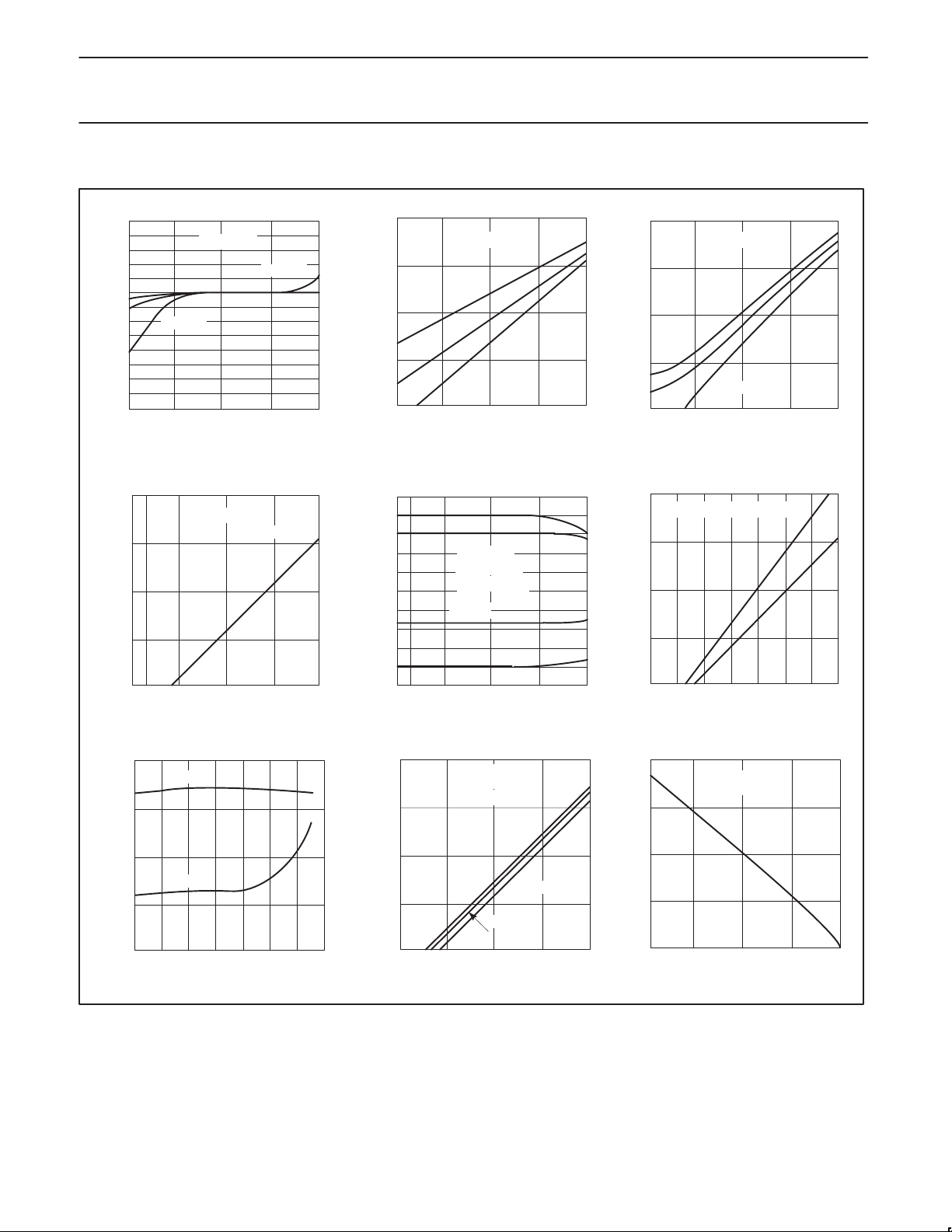
TYPICAL PERFORMANCE CHARACTERISTICS
Input Offset Voltage
VS = ±15V
-55°C
+25°C
+125°C
0.1µA1µA10µA 100µA 1000µA
AMPLIFIER BIAS CURRENT (I
Peak Output Current
VS = ±15V
0.1µA1µA10µA 100µA 1000µA
AMPLIFIER BIAS CURRENT (I
INPUT OFFSET VOLTAGE (mV)
µ
PEAK OUTPUT CURRENT ( A)
5
4
3
2
1
0
-1
-2
-3
-4
-5
-6
-7
-8
4
10
3
10
2
10
10
1
+125°C
ABC
+125°C
ABC
)
+25°C
-55°C
3
10
2
10
10
1
INPUT OFFSET CURRENT (nA)
0.1
5
4
3
2
1
0
-1
-2
-3
-4
-5
COMMON-MODE RANGE (V)
-6
PEAK OUTPUT VOLTAGE AND
-7
-8
)
Input Bias Current
VS = ±15V
-55°C
+25°C
0.1µA1µA10µA 100µA 1000µA
AMPLIFIER BIAS CURRENT (I
Peak Output Voltage and
Common-Mode Range
V
OUT
V
CMR
VS = ±15V
RLOAD = ∞
T
amb
V
CMR
V
OUT
0.1µA1µA10µA 100µA 1000µA
AMPLIFIER BIAS CURRENT (I
+125°C
= 25°C
ABC
ABC
NE5517/NE5517A/
AU5517
4
10
3
10
2
10
10
INPUT BIAS CURRENT (nA)
1
)
5
10
4
10
3
10
2
10
LEAKAGE CURRENT (pA)
10
-50°C -25°C0°C25°C50°C75°C100°C125°C
)
Input Bias Current
VS = ±15V
-55°C
+25°C
0.1µA1µA10µA 100µA 1000µA
AMPLIFIER BIAS CURRENT (I
+125°C
ABC
)
Leakage Current
(+)VIN = (–)VIN = V
AMBIENT TEMPERATURE (TA)
OUT
= 36V
0V
4
10
3
10
2
10
10
INPUT LEAKAGE CURRENT (pA)
1
012345 67
Input Leakage
+125°C
+25°C
INPUT DIFFERENTIAL VOLTAGE
2002 Dec 06
5
10
µ
4
10
3
10
2
10
TRANSCONDUCTANCE (gM) — ( ohm)
10
Transconductance
gM
0.1µA1µA10µA 100µA 1000µA
AMPLIFIER BIAS CURRENT (I
PINS 2, 15
VS = ±15V
-55°C
OPEN
+25°C
+125°C
ABC
)
mq
m
M
Figure 4. Typical Performance Characteristics
6
2
10
Ω
1
10
1
0.1
INPUT RESISTANCE (MEG )
0.01
Input Resistance
PINS 2, 15
OPEN
0.1µA1µA10µA 100µA 1000µA
AMPLIFIER BIAS CURRENT (I
ABC
SL00309
)
Page 7

Philips Semiconductor Product data
Dual operational transconductance amplifier
TYPICAL PERFORMANCE CHARACTERISTICS (Continued)
Amplifier Bias Voltage vs
2000
1800
1600
1400
1200
1000
800
600
400
AMPLIFIER BIAS VOLTAGE (mV)
200
0
0.1µA1µA10µA 100µA 1000µA
-55°C
+25°C
+125°C
AMPLIFIER BIAS CURRENT (I
Voltage vs Amplifier Bias Current Noise vs Frequency
20
0
-20
-40
-60
1 VOLT RMS (dB)
-80
OUTPUT VOLTAGE RELATIVE TO
-100
0.1µA1µA10µA 100µA 1000µA
I
ABC
Amplifier Bias Current
)
ABC
VS = ±15V
RL = 10kΩ
VIN = 80mV
P-P
OUTPUT NOISE
20kHz BW
AMPLIFIER BIAS CURRENT (µA)
Figure 5. Typical Performance Characteristics (cont.)
Input and Output Capacitance
7
VS = ±15V
6
5
4
3
CAPACITANCE (pF)
2
1
0
0.1µA1µA10µA 100µA 1000µA
AMPLIFIER BIAS CURRENT (I
VIN = 40mV
P-P
T
amb
C
IN
C
OUT
= +25°C
NE5517/NE5517A/
Distortion vs Differential
100
RL = 10kΩ
I
= 1mA
ABC
10
1
0.1
OUTPUT DISTORTION (%)
0.01
1 10 100 1000
)
ABC
600
500
400
300
200
100
OUTPUT NOISE CURRENT (pA/Hz)
0
10 100 1k 10k 100k
FREQUENCY (Hz)
DIFFERENTIAL INPUT VOLTAGE (mV
I
ABC
I
= 100µA
ABC
Input Voltage
= 1mA
AU5517
)
P-P
SL00310
2002 Dec 06
7
Page 8

Philips Semiconductor Product data
Dual operational transconductance amplifier
TYPICAL PERFORMANCE CHARACTERISTICS (Continued)
+36V
4, 13
2, 15
3, 14
–
+
A
Leakage Current Test Circuit Differential Input Current Test Circuit
NE5517
11
7, 10
5, 12
1, 15
6
8, 9
V+
NE5517/NE5517A/
AU5517
+15V
4V
A
4, 13
2, 15
3, 14
–
+
11
5, 12
NE5517
1, 10
6
–15V
APPLICATIONS
INPUT
V
50kΩ
V–
Buffer V
Test Circuit
BE
Figure 6. Typical Performance Characteristics (cont.)
+15V
10k
390pF
51Ω
1.3k
3, 14
2, 15
4, 13
–
+
NE5517
10k
11
6
–15V
0.001µF
1, 16
0.01µF
Unity Gain Follower
Figure 7. Applications
62k
5, 12
7, 10
0.01µF
8, 9
5k
–15V
SL00311
OUTPUT
SL00312
2002 Dec 06
8
Page 9

Philips Semiconductor Product data
Dual operational transconductance amplifier
CIRCUIT DESCRIPTION
The circuit schematic diagram of one-half of the AU5517/NE5517, a
dual operational transconductance amplifier with linearizing diodes
and impedance buffers, is shown in Figure 8.
1. Transconductance Amplifier
The transistor pair, Q4 and Q5, forms a transconductance stage. The
ratio of their collector currents (I
the differential input voltage, V
I
5
KT
+
V
IN
Where V
In
q
I
4
is the difference of the two input voltages
IN
KT ≅ 26 mV at room temperature (300 °k).
Transistors Q
the sum of current I
I
+ I
4
, Q2 and diode D1 form a current mirror which focuses
1
and I5 to be equal to amplifier bias current IB:
4
= I
5
B
If VIN is small, the ratio of I5 and I4 will approach unity and the Taylor
series of In function can be approximated as
KT
q
and I
KT
q
I
* I4+ V
5
In
≅ I5 ≅ I
4
I
In
I
I
5
I
4
5
[
4
I5* I
KT
[
q
I
4
B
I5* I
KT
4
1ń2I
ǒ
I
B
2KT
+
B
q
Ǔ
q
IN
The remaining transistors (Q6 to Q11) and diodes (D4 to D6) form
three current mirrors that produce an output current equal to I
minus I4. Thus:
q
ǒ
V
IN
The term
proportional to I
Ǔ
I
B
+ I
2KT
O
q
ǒ
Ǔ
I
B
is then the transconductance of the amplifier and is
2KT
.
B
2. Linearizing Diodes
For VIN greater than a few millivolts, equation 3 becomes invalid and
the transconductance increases non-linearly. Figure 9 shows how
the internal diodes can linearize the transfer function of the
operational amplifier. Assume D
sources and the input signal current is I
I
4
I
4
+ I
= (I
= IB and I
5
– I0), I
B
5
5
= (I
– I
= I0, that is:
4
+ I0)
B
and I5, respectively) is defined by
4
, which is shown in equation 1.
IN
4
I5* I
2KT
q
4
+ V
. Since
S
IN
I
B
and D3 are biased with current
2
(1)
(2)
(3)
(4)
5
(5)
NE5517/NE5517A/
AU5517
For the diodes and the input transistors that have identical
geometries and are subject to similar voltages and temperatures,
the following equation is true:
I
D
) I
I
2
D
2
S
* I
2IB
I
D
S
KT
+
q
S
for |IS| t
In
T
In
q
I
+ I
O
The only limitation is that the signal current should not exceed ID.
3. Impedance Buffer
The upper limit of transconductance is defined by the maximum
value of I
(2 mA). The lowest value of IB for which the amplifier will
B
function therefore determines the overall dynamic range. At low
values of I
, a buffer with very low input bias current is desired. A
B
Darlington amplifier with constant-current source (Q
D
, and R1) suits the need.
8
APPLICATIONS
Voltage-Controlled Amplifier
In Figure 10, the voltage divider R2, R3 divides the input-voltage into
small values (mV range) so the amplifier operates in a linear
manner.
It is:
R
I
+*V
+ I
V
OUT
V
IN
= 19.2 I
M
IN
OUT
+
OUT
V
OUT
A +
(3) g
(gM in µmhos for I
Since g
is directly proportional to I
M
controlled by the voltage V
When VC is taken relative to –VCC the following formula is valid:
* 1.2V)
(V
I
ABC
C
+
R
The 1.2 V is the voltage across two base-emitter baths in the current
mirrors. This circuit is the base for many applications of the
AU5517/NE5517.
@
R2) R
@ RL;
R
R2) R
ABC
ABC
1
3
3
3
in mA)
) IO)
1ń2(I
B
1ń2(I
* IO)
B
I
D
2
@ gM;
3
@ gM @ R
L
ABC
in a simple way.
C
, Q15, Q16, D7,
14
, the amplification is
(6)
2002 Dec 06
9
Page 10

Philips Semiconductor Product data
Dual operational transconductance amplifier
V+
11
2,15
–INPUT
AMP BIAS
INPUT
V–
6
Q6
D2
Q4
4,13
1,16
Q1
D1
Q2
Q7
Q5
D4
Q10
Q11
D3
+INPUT
3,14
Q9
Q8
Figure 8. Circuit Diagram of NE5517
NE5517/NE5517A/
AU5517
D6
Q14
V
OUTPUT
5,12
Q15 Q16
R1
D5
7,10
D7
D8
Q12
Q13
8,9
Q3
SL00313
+V
S
I
D
I
B
S
I
D
SL00314
–V
I
B
S
I0 2I
4
I
5
I
5
I
D
2
1/2I
I
S
I
S
I
D
I
D
3
D
S
1/2I
I
S
2
D
D
2
I0 I5 I
I
4
Q
4
Figure 9. Linearizing Diode
Stereo Amplifier With Gain Control
Figure 1 1 shows a stereo amplifier with variable gain via a control
input. Excellent tracking of typical 0.3 dB is easy to achieve. With
the potentiometer, R
, the offset can be adjusted. For AC-coupled
P
amplifiers, the potentiometer may be replaced with two 510 Ω
resistors.
Modulators
Because the transconductance of an OTA (Operational
Transconductance Amplifier) is directly proportional to I
amplification of a signal can be controlled easily. The output current
is the product from transconductance×input voltage. The circuit is
effective up to approximately 200 kHz. Modulation of 99% is easy to
achieve.
ABC
, the
Voltage-Controlled Resistor (VCR)
Because an OTA is capable of producing an output current
proportional to the input voltage, a voltage variable resistor can be
made. Figure 13 shows how this is done. A voltage presented at the
RX terminals forces a voltage at the input. This voltage is multiplied
by g
and thereby forces a current through the RX terminals:
M
R R
gM R
A
A
R
=
X
where gM is approximately 19.21 µMHOs at room temperature.
Figure 14 shows a Voltage Controlled Resistor using linearizing
diodes. This improves the noise performance of the resistor.
Voltage-Controlled Filters
Figure 15 shows a Voltage Controlled Low-Pass Filter. The circuit is
a unity gain buffer until X
is equal to R/RA. Then, the frequency
C/gM
response rolls off at a 6dB per octave with the –3 dB point being
defined by the given equations. Operating in the same manner, a
Voltage Controlled High-Pass Filter is shown in Figure 16. Higher
order filters can be made using additional amplifiers as shown in
Figures 17 and 18.
Voltage-Controlled Oscillators
Figure 19 shows a voltage-controlled triangle-square wave
generator. With the indicated values a range from 2 Hz to 200 kHz is
possible by varying I
The output amplitude is determined by I
Please notice the differential input voltage is not allowed to be above
5 V.
With a slight modification of this circuit you can get the sawtooth
pulse generator, as shown in Figure 20.
from 1 mA to 10 µA.
ABC
OUT
× R
OUT
.
2002 Dec 06
10
Page 11

Philips Semiconductor Product data
Dual operational transconductance amplifier
APPLICATION HINTS
To hold the transconductance gM within the linear range, I
should be chosen not greater than 1 mA. The current mirror ratio
should be as accurate as possible over the entire current range. A
current mirror with only two transistors is not recommended. A
suitable current mirror can be built with a PNP transistor array which
causes excellent matching and thermal coupling among the
V
R4 = R2/ /R
IN
3
R
2
ABC
V
C
+V
CC
R
11
NE5517
6
TYPICAL VALUES:
1
1
I
OUT
3
+
–
4
R
3
Figure 10.
NE5517/NE5517A/
AU5517
transistors. The output current range of the DAC normally reaches
from 0 to –2 mA. In this application, however, the current range is
set through R
I
DACMAX
I
ABC
5
R
L
R
R2 = 10k
R
R
R
RS = 47k
7
= 47k
1
= 200Ω
3
= 200Ω
4
= 100k
L
(10 kΩ) to 0 to –1 mA.
REF
V
REF
2
2
R
REF
8
R
S
SL00315
5V
1mA
10kW
INT
+V
CC
V
OUT
INT
–V
CC
+V
CC
30k
R
10k
R
10k
R
C
IN
R
P
1k
+V
CC
IN
R
P
1k
+V
CC
V
IN1
V
C
V
IN2
15k
R
15k
R
3
+
11
15
4
14
13
NE5517/A
–
+
NE5517/A
–
I
ABC
1
R
L
10k
16
I
ABC
6
10
12
R
L
10k
D
D
5.1k
R
INT
+V
CC
8
V
OUT1
–V
CC
+V
CC
9
V
OUT2
S
–V
CC
INT
SL00316
Figure 11. Gain-Controlled Stereo Amplifier
2002 Dec 06
11
Page 12

Philips Semiconductor Product data
Dual operational transconductance amplifier
R
C
V
IN2
SIGNAL
V
IN1
CARRIER
200
200
V
OS
10k
3
2
4
30k
I
ABC
I
D
15k
1k
2
3
4
+V
CC
+
NE5517/A
–
–V
CC
Figure 12. Amplitude Modulator
+V
CC
11
+
NE5517/A
–
–V
CC
I
O
5
Figure 13. VCR
11
6
30k
7
C
R
X
100k
NE5517/NE5517A/
AU5517
1
INT
+V
CC
5
8
R
10k
R
10k
7
8
R
S
R R
gM R
A
A
V
–V
INT
OUT
CC
SL00317
SL00318
L
RX
V
C
INT
+V
CC
V
OUT
–V
CC
INT
2002 Dec 06
+V
CC
2
3
4
+V
NE5517/A
–V
CC
I
D
R
OS
P
1k
V
1
CC
11
5
6
30k
7
C
R
X
100k
8
R
10k
+V
–V
INT
V
INT
C
CC
CC
SL00319
Figure 14. VCR with Linearizing Diodes
12
Page 13

Philips Semiconductor Product data
Dual operational transconductance amplifier
1
+V
CC
NOTE:
fO
V
NULL
NOTE:
fO
OS
V
-V
100k
IN
RAg
g(R RA) 2pC
+V
CC
100k
CC
1k
RAg
M
g(R RA) 2pC
200
M
Figure 15. Voltage-Controlled Low-Pass Filter
Figure 16. Voltage-Controlled High-Pass Filter
3
2
R
A
3
2
4
R
A
1k
+
NE5517/A
–
4
200
+V
+
NE5517/A
–
–V
–V
CC
CC
11
6
150pF
CC
1
I
ABC
11
6
0.005µF
I
ABC
5
NE5517/NE5517A/
AU5517
30k
5
7
C
R
100k
30k
7
C
R
100k
10k
10k
SL00320
8
SL00321
V
C
INT
+V
CC
8
V
OUT
–V
CC
INT
V
C
INT
+V
CC
V
OUT
–V
CC
INT
V
IN
NOTE:
fO
2002 Dec 06
200
R
A
200
RAg
M
(R RA)2p C
+V
CC
+
NE5517/A
–
–V
CC
+V
CC
+
NE5517/A
–
A
R
A
200
C
100pF
100k
100k
R
200
10k
-V
100k
CC
R
Figure 17. Butterworth Filter – 2nd Order
13
15k
200pF
2C
10k
V
C
INT
+V
CC
V
OUT
–V
CC
INT
SL00322
Page 14

Philips Semiconductor Product data
Dual operational transconductance amplifier
1
+V
10k
CC
3
+
11
2
NE5517/A
–
6
1k
–V
CC
5
7
800pF
20k
Figure 18. State Variable Filter
3
4
30k
–
NE5517/A
+
–V
11
6
CC
+V
CC
1
5
7
C
0.1µF
20k
–V
CC
V
C
INT
V
+V
8
OUT1
5.1k
–V
+V
20k
CC
CC
CC
1k
BANDPASS OUT
13
–
NE5517/A
+
14
NE5517/NE5517A/
AU5517
800pF
9
20k
15k
10k
INT
+V
CC
V
OUT2
–V
CC
INT
GAIN
CONTROL
LOW
PASS
V
OUT
5.1k
SL00323
V
C
INT
+V
CC
9
–V
CC
INT
16
14
+
NE5517/A
15
–
13
+V
CC
47k
12 10
16
12 10
NOTE:
(VC 0.8) R
VPK
2002 Dec 06
R1 R
SL00324
Figure 19. Triangle-Square Wave Generator (VCO)
I
1
TL
B
5
C
0.1µF
2VPKxC
I
C
f
OSC
7
20k
–V
CC
I
C
2VPKxC
INT
+V
CC
8
V
OUT1
ICI
13
14
–
NE5517/A
+
B
+V
CC
16
47k
12 10
R
2
30k
INT
+V
CC
30k
–V
CC
V
OUT2
INT
SL00325
I
C
4
2
3
TH
470k
+V
+
11
NE5517/A
–
6
–V
CC
2VPKxC
I
B
CC
V
C
R
1
30k
1
2
Figure 20. Sawtooth Pulse VCO
14
Page 15

Philips Semiconductor Product data
Dual operational transconductance amplifier
NE5517/NE5517A/
AU5517
DIP16: plastic dual in-line package; 16 leads (300 mil) SOT38-4
2002 Dec 06
15
Page 16

Philips Semiconductor Product data
Dual operational transconductance amplifier
NE5517/NE5517A/
AU5517
SO16: plastic small outline package; 16 leads; body width 3.9 mm SOT109-1
2002 Dec 06
16
Page 17

Philips Semiconductor Product data
Dual operational transconductance amplifier
NE5517/NE5517A/
AU5517
REVISION HISTORY
Rev Date Description
_3 20021206 Product data (9397 750 10796); type number AU5517 added. ECN 853–0887 29176 of 08 November 2002;
_2 20010803 Product data (9397 750 09175); NE5517/NE5517A only; ECN 853–0887 26833 of 2001 Aug 03 .
supersedes Product data NE5517_NE5517A version 2 of 03 August 2001.
Modifications:
•Type number AU5517 added.
•“Description” section edited.
2002 Dec 06
17
Page 18

Philips Semiconductor Product data
Dual operational transconductance amplifier
NE5517/NE5517A/
AU5517
Data sheet status
Product
Level
I
II
III
[1] Please consult the most recently issued data sheet before initiating or completing a design.
[2] The product status of the device(s) described in this data sheet may have changed since this data sheet was published. The latest information is available on the Internet at URL
[3] For data sheets describing multiple type numbers, the highest-level product status determines the data sheet status.
Data sheet status
Objective data
Preliminary data
Product data
http://www.semiconductors.philips.com.
[1]
[2] [3]
status
Development
Qualification
Production
Definitions
This data sheet contains data from the objective specification for product development.
Philips Semiconductors reserves the right to change the specification in any manner without notice.
This data sheet contains data from the preliminary specification. Supplementary data will be published
at a later date. Philips Semiconductors reserves the right to change the specification without notice, in
order to improve the design and supply the best possible product.
This data sheet contains data from the product specification. Philips Semiconductors reserves the
right to make changes at any time in order to improve the design, manufacturing and supply. Relevant
changes will be communicated via a Customer Product/Process Change Notification (CPCN).
Definitions
Short-form specification — The data in a short-form specification is extracted from a full data sheet with the same type number and title. For detailed information see
the relevant data sheet or data handbook.
Limiting values definition — Limiting values given are in accordance with the Absolute Maximum Rating System (IEC 60134). Stress above one or more of the limiting
values may cause permanent damage to the device. These are stress ratings only and operation of the device at these or at any other conditions above those given
in the Characteristics sections of the specification is not implied. Exposure to limiting values for extended periods may affect device reliability.
Application information — Applications that are described herein for any of these products are for illustrative purposes only. Philips Semiconductors make no
representation or warranty that such applications will be suitable for the specified use without further testing or modification.
Disclaimers
Life support — These products are not designed for use in life support appliances, devices, or systems where malfunction of these products can reasonably be
expected to result in personal injury . Philips Semiconductors customers using or selling these products for use in such applications do so at their own risk and agree
to fully indemnify Philips Semiconductors for any damages resulting from such application.
Right to make changes — Philips Semiconductors reserves the right to make changes in the products—including circuits, standard cells, and/or software—described
or contained herein in order to improve design and/or performance. When the product is in full production (status ‘Production’), relevant changes will be communicated
via a Customer Product/Process Change Notification (CPCN). Philips Semiconductors assumes no responsibility or liability for the use of any of these products, conveys
no license or title under any patent, copyright, or mask work right to these products, and makes no representations or warranties that these products are free from patent,
copyright, or mask work right infringement, unless otherwise specified.
Contact information
For additional information please visit
http://www.semiconductors.philips.com . Fax: +31 40 27 24825
For sales offices addresses send e-mail to:
sales.addresses@www.semiconductors.philips.com.
Document order number: 9397 750 10796
Koninklijke Philips Electronics N.V. 2002
All rights reserved. Printed in U.S.A.
Date of release: 12-02
2002 Dec 06
18
 Loading...