

Philips NE5204A Service Manual
INTEGRATED CIRCUITS
NE/SA5204A
Wide-band high-frequency amplifier
Product specification 1992 Feb 25
RF Communications Handbook
Philips Semiconductors
Philips Semiconductors Product specification
NE/SA5204AWide-band high-frequency amplifier
DESCRIPTION
The NE/SA5204A family of wideband amplifiers replaces the
NE/SA5204 family . The ‘A’ parts are fabricated on a rugged 2µm
bipolar process featuring excellent statistical process control.
Electrical performance is nomically identical to the original parts.
The NE/SA5204A is a high-frequency amplifier with a fixed insertion
gain of 20dB. The gain is flat to ±0.5dB from DC to 200MHz. The
-3dB bandwidth is greater than 350MHz. This performance makes
the amplifier ideal for cable TV applications. The NE/SA5204A
operates with a single supply of 6V, and only draws 25mA of supply
current, which is much less than comparable hybrid parts. The noise
figure is 4.8dB in a 75Ω system and 6dB in a 50Ω system.
The NE/SA5204A is a relaxed version of the NE5205. Minimum
guaranteed bandwidth is relaxed to 350MHz and the “S” parameter
Min/Max limits are specified as typicals only.
Until now, most RF or high-frequency designers had to settle for
discrete or hybrid solutions to their amplification problems. Most of
these solutions required trade-offs that the designer had to accept in
order to use high-frequency gain stages. These include high power
consumption, large component count, transformers, large packages
with heat sinks, and high part cost. The NE/SA5204A solves these
problems by incorporating a wideband amplifier on a single
monolithic chip.
The part is well matched to 50 or 75Ω input and output impedances.
The standing wave ratios in 50 and 75Ω systems do not exceed 1.5
on either the input or output over the entire DC to 350MHz operating
range.
Since the part is a small, monolithic IC die, problems such as stray
capacitance are minimized. The die size is small enough to fit into a
very cost-effective 8-pin small-outline (SO) package to further
reduce parasitic effects.
No external components are needed other than AC-coupling
capacitors because the NE/SA5204A is internally compensated and
matched to 50 and 75Ω. The amplifier has very good distortion
specifications, with second and third-order intermodulation
intercepts of +24dBm and +17dBm, respectively, at 100MHz.
The part is well matched for 50Ω test equipment such as signal
generators, oscilloscopes, frequency counters, and all kinds of
signal analyzers. Other applications at 50Ω include mobile radio, CB
radio, and data/video transmission in fiber optics, as well as
broadband LANs and telecom systems. A gain greater than 20dB
can be achieved by cascading additional NE/SA5204As in series as
required, without any degradation in amplifier stability.
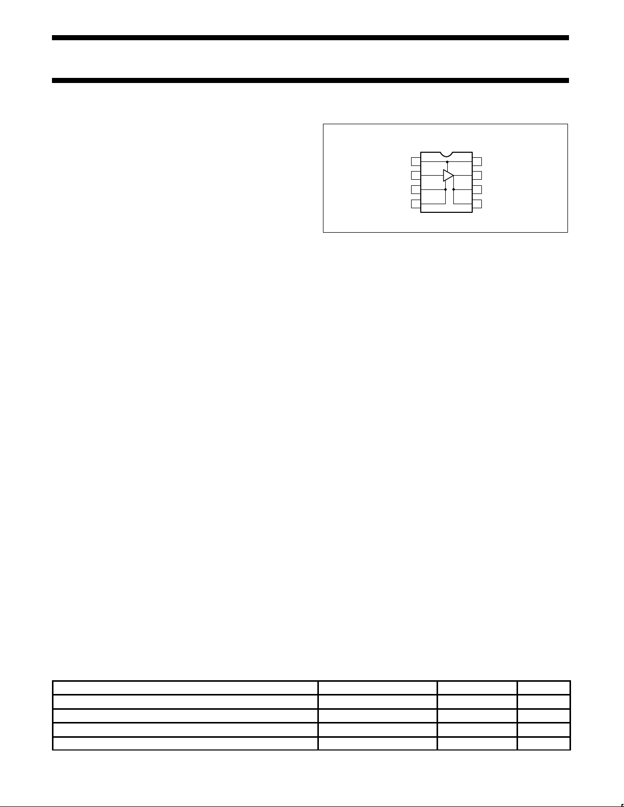
PIN CONFIGURA TION
N, D Packages
1
V
CC
2
V
IN
3
GND
GND
TOP VIEW
Figure 1. Pin Configuration
20dB
8
V
CC
7
V
OUT
6
GND
54
GND
FEATURES
•Bandwidth (min.)
200 MHz, ±0.5dB
350 MHz, -3dB
•20dB insertion gain
•4.8dB (6dB) noise figure Z
=75Ω (ZO=50Ω)
O
•No external components required
•Input and output impedances matched to 50/75Ω systems
•Surface-mount package available
•Cascadable
•2000V ESD protection
APPLICATIONS
•Antenna amplifiers
•Amplified splitters
•Signal generators
•Frequency counters
•Oscilloscopes
•Signal analyzers
•Broadband LANs
•Networks
•Modems
•Mobile radio
•Security systems
•Telecommunications
SR00193
ORDERING INFORMATION
DESCRIPTION TEMPERATURE RANGE ORDER CODE DWG #
8-Pin Plastic Dual In-Line Package (DIP) 0 to +70°C NE5204AN SOT97-1
8-Pin Plastic Small Outline (SO) package 0 to +70°C NE5204AD SOT96-1
8-Pin Plastic Dual In-Line Package (DIP) –40 to +85°C SA5204AN SOT97-1
8-Pin Plastic Small Outline (SO) package –40 to +85°C SA5204AD SOT96-1
1992 Feb 25 853-1599 05790
2
Philips Semiconductors Product specification
NE/SA5204AWide-band high-frequency amplifier
ABSOLUTE MAXIMUM RATINGS
SYMBOL PARAMETER RATING UNIT
V
CC
V
IN
T
A
P
DMAX
T
J
T
STG
T
SOLD
NOTES:
1. Derate above 25°C, at the following rates
N package at 9.3mW/°C
D package at 6.2mW/°C
2. See “Power Dissipation Considerations” section.
Supply voltage 9 V
AC input voltage 5 V
P–P
Operating ambient temperature range
NE grade 0 to +70 °C
SA grade –40 to +85 °C
Maximum power dissipation
1, 2
TA=25°C(still–air)
N package 1160 mW
D package 780 mW
Junction temperature 150 °C
Storage temperature range –55 to +150 °C
Lead temperature
(soldering 60s)
300 °C
EQUIVALENT SCHEMATIC
V
IN
V
CC
R
1
Q
3
Q
1
R
E1
Q
4
R
F1
R
F2
Figure 2. Equivalent Schematic
R
2
R
0
Q
6
Q
2
R
3
R
E2
Q
5
V
OUT
SR00194
1992 Feb 25
3
Philips Semiconductors Product specification
SYMBOL
PARAMETER
TEST CONDITIONS
UNIT
S11
I
dB
S22
Output
dB
S12
Isolati
dB
NE/SA5204AWide-band high-frequency amplifier
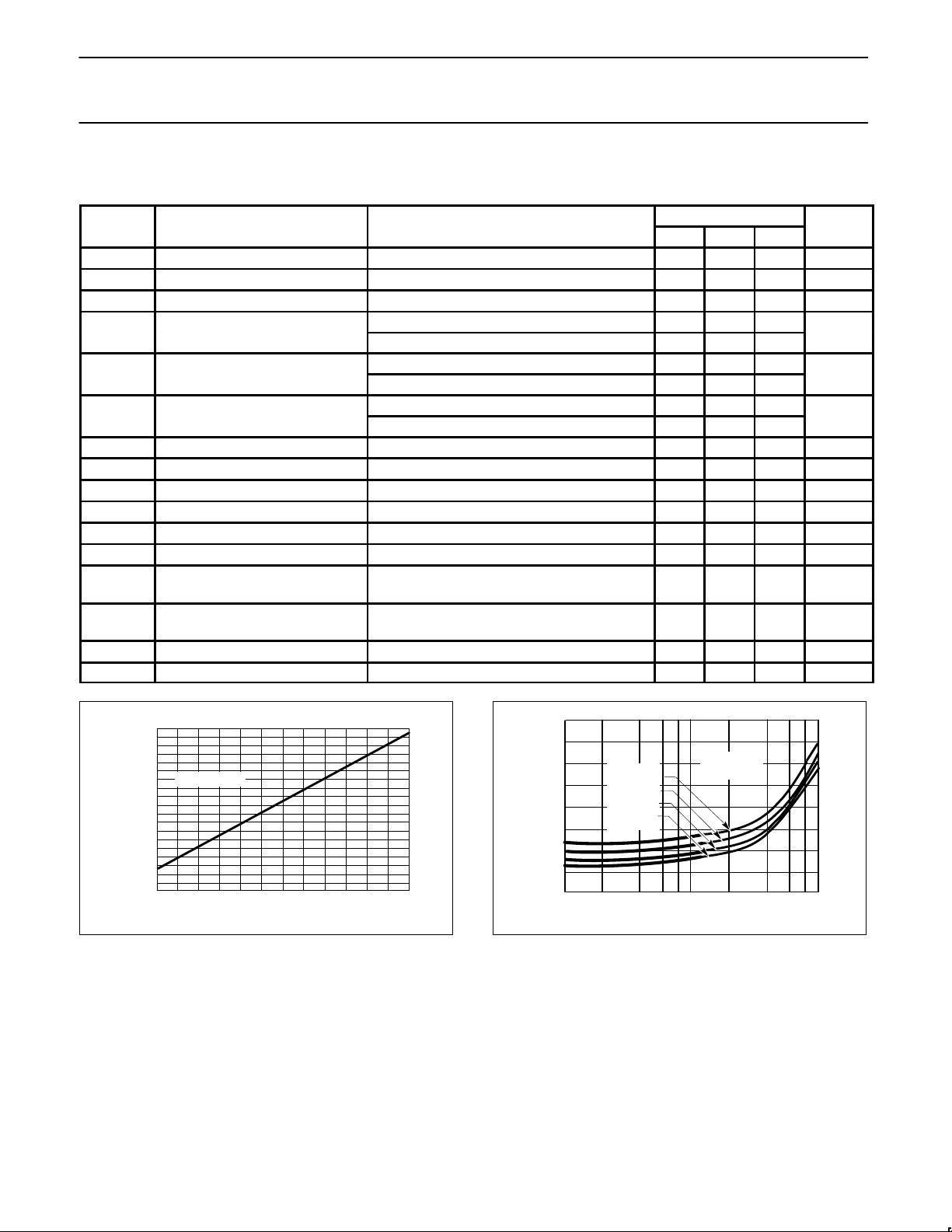
DC ELECTRICAL CHARACTERISTICS
VCC=6V, ZS=ZL=ZO=50Ω and TA=25°C, in all packages, unless otherwise specified.
LIMITS
Min Typ Max
V
CC
I
CC
S21 Insertion gain f=100MHz, over temperature 16 19 22 dB
BW Bandwidth ±0.5dB 200 350 MHz
BW Bandwidth –3dB 350 550 MHz
t
R
t
P
Operating supply voltage range Over temperature 5 8 V
Supply current Over temperature 19 25 33 mA
nput return loss
return loss
on
f=100MHz 25
DC –550MHz 12
f=100MHz 27
DC –550MHz 12
f=100MHz –25
DC –550MHz –18
Noise figure (75Ω) f=100MHz 4.8 dB
Noise figure (50Ω) f=100MHz 6.0 dB
Saturated output power f=100MHz +7.0 dBm
1dB gain compression f=100MHz +4.0 dBm
Third–order intermodulation inter-
cept (output)
Second–order intermodulation inter-
cept (output)
f=100MHz +17 dBm
f=100MHz +24 dBm
Rise time 500 ps
Propagation delay 500 ps
35
34
32
30
28
26
24
22
20
SUPPLY CURRENT—mA
18
16
TA = 25oC
5 5.5 6 6.5 7 7.5 8
SUPPLY VOLTAGE—V
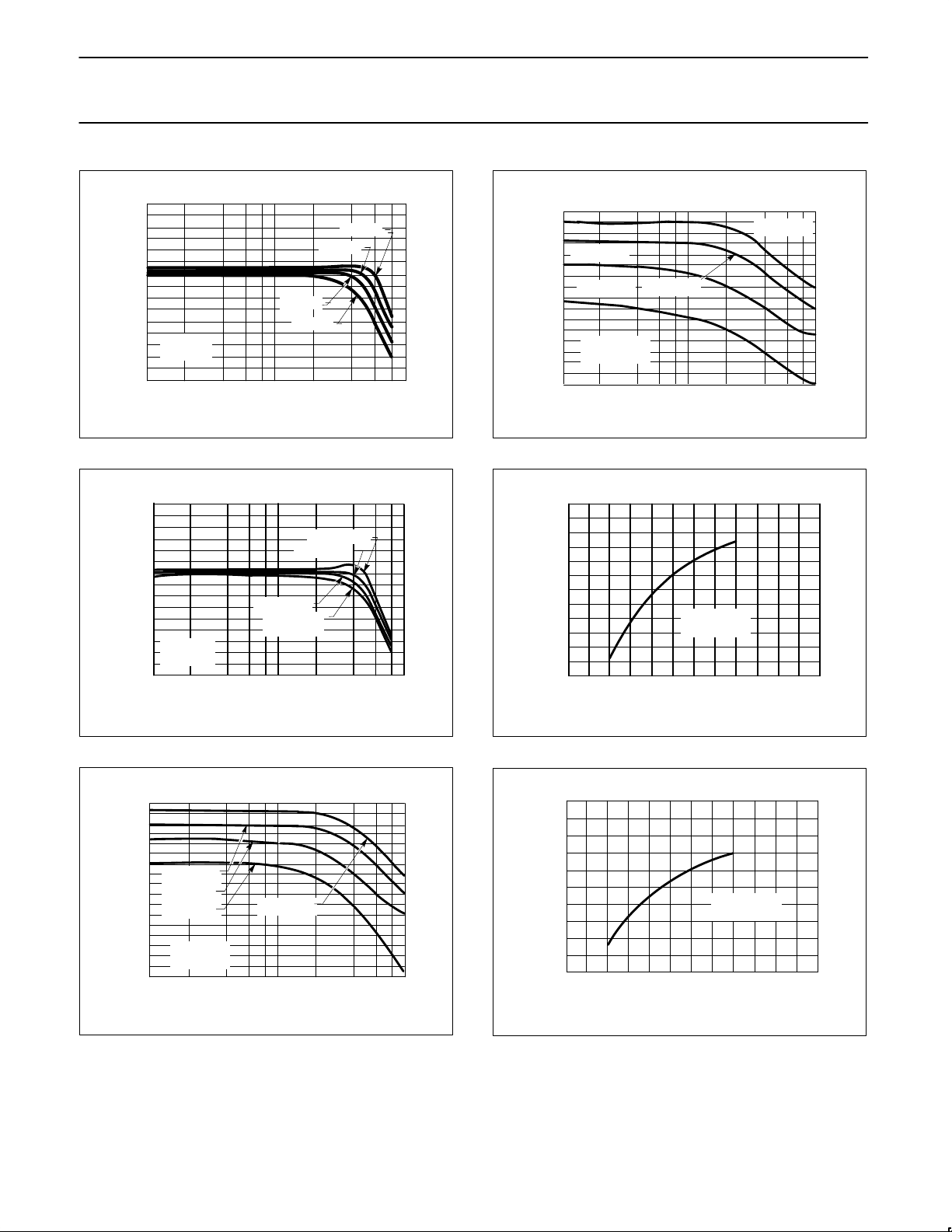
Figure 3. Supply Current vs Supply Voltage
SR00195
9
8
7
NOISE FIGURE—dBm
6
5
10
vcc = 8v
vcc = 7v
vcc = 6v
vcc = 5v
12 468 2 468
ZO = 50Ω
= 25oC
T
A
2
10
FREQUENCY—MHz
Figure 4. Noise Figure vs Frequency
3
10
SR00196
1992 Feb 25
4
Philips Semiconductors Product specification
NE/SA5204AWide-band high-frequency amplifier
25
vcc = 8v
v
= 7v
20
15
ZO = 50Ω
INSERTION GAIN—dB
= 25oC
T
A
10
12 468 2 468
10
10
FREQUENCY—MHz
cc
vcc = 6v
vcc = 5v
2
Figure 5. Insertion Gain vs Frequency (S21)
25
TA = 55oC
TA = 85oC
TA =
125oC
2
10
TA = 25oC
20
15
INSERTION GAIN—dB
VCC = 8V
= 50Ω
Z
O
10
12 468 2 468
10
FREQUENCY—MHz
Figure 6. Insertion Gain vs Frequency (S21)
3
10
SR00197
3
10
SR00199
10
9
8
7
6
V
6V
CC =
5
4
3
V
CC =
2
1
0
–1
–2
OUTPUT LEVEL—dBm
–3
–4
–5
–6
ZO = 50Ω
T
A
12 468 2 468
10
5V
= 25oC
V
7V
CC =
2
10
FREQUENCY—MHz
V
CC =
8V
3
10
SR00198
Figure 8. 1dB Gain Compression vs Frequency
40
35
30
25
20
15
SECOND–ORDER INTERCEPT—dBm
10
45678910
POWER SUPPLY VOLTAGE—V
ZO = 50Ω
= 25oC
T
A
SR00200
Figure 9. Second-Order Output Intercept vs Supply Voltage
11
10
9
8
7
6
5
4
VCC = 7V
3
2
VCC = 6V
1
VCC = 5V
0
–1
–2
–3
OUTPUT LEVEL—dBm
ZO = 50Ω
–4
–5
–6
= 25oC
T
A
12 468 2 468
10
VCC = 8V
2
FREQUENCY—MHz
10
Figure 7. Saturated Output Power vs Frequency
1992 Feb 25
3
10
SR00201
30
25
20
15
10
THIRD–ORDER INTERCEPT—dBm
5
45678910
POWER SUPPLY VOLTAGE—V
ZO = 50Ω
= 25oC
T
A
SR00202
Figure 10. Third-Order Intercept vs Supply Voltage
5
 Loading...