

Philips N74F32N, N74F32D Datasheet
INTEGRATED CIRCUITS
74F32
Quad 2-input OR gate
Product specification
IC15 Data Handbook
1990 Oct 04
Philips Semiconductors Product specification
74F32Quad 2-input OR gate
FEA TURE
•Industrial temperature range available (–40°C to +85°C)
TYPE
74F32 4.1ns 8.2mA
TYPICAL
PROPAGATION
DELAY
TYPICAL
SUPPLY CURRENT
(TOTAL)
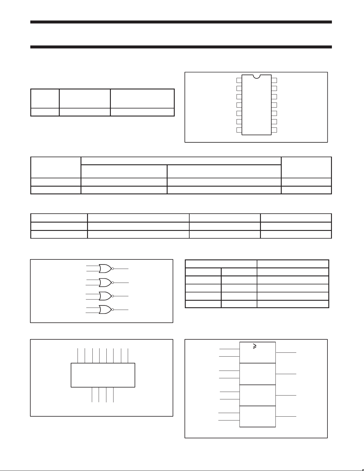
PIN CONFIGURATION
D0a
1
D0b
2
Q0
3
D1a
4
D1b
5
Q1
6
GND
14
V
CC
D3b
13
D3a
12
Q3
11
D2b
10
D2a
9
Q2
87
SF00038
ORDERING INFORMA TION
ORDER CODE
DESCRIPTION
COMMERCIAL RANGE
VCC = 5V ±10%, T
= 0°C to +70°C
amb
VCC = 5V ±10%, T
INDUSTRIAL RANGE
= –40°C to +85°C
amb
PKG DWG #
14-pin plastic DIP N74F32N I74F32N SOT27-1
14-pin plastic SO N74F32D I74F32D SOT108–1
INPUT AND OUTPUT LOADING AND FAN OUT TABLE
PINS DESCRIPTION 74F (U.L.) HIGH/LOW LOAD VALUE HIGH/LOW
Dna, Dnb Data inputs 1.0/1.0 20µA/0.6mA
Qn Data output 50/33 1.0mA/20mA
NOTE: One (1.0) FAST unit load is defined as: 20µA in the high state and 0.6mA in the low state.
LOGIC DIAGRAM
VCC = Pin 14
GND = Pin 7
LOGIC SYMBOL
= Pin 14
V
CC
GND = Pin 7
1
D0a
2
D0b
4
D1a
5
D1b
9
D2a
10
D2b
12
D3a
13
D3b
12459101213
D0a D0bD1a D2a D2b D3a D3bD1b
Q0 Q1 Q2 Q3
36811
3
6
8
11
SF00039
SF00040
Q3
Q0
Q1
Q2
FUNCTION TABLE
INPUTS OUTPUT
Dna Dnb Qn
L L L
L H H
H L H
H H H
NOTES:
1 H = High voltage level
2 L = Low voltage level
IEC/IEEE SYMBOL
1
2
4
5
9
10
12
13
1
3
6
8
11
SF00041
October 4, 1990 853 0333 00624
2
Philips Semiconductors Product specification
T
Operating free air temperature range
T
Operating free air temperature range
74F32Quad 2-input OR gate
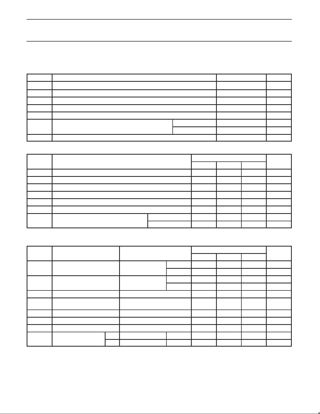
ABSOLUTE MAXIMUM RATINGS
(Operation beyond the limit set forth in this table may impair the useful life of the device.
Unless otherwise noted these limits are over the operating free air temperature range.)
SYMBOL
V
V
I
IN
V
I
OUT
T
CC
IN
OUT
amb
stg
Supply voltage
Input voltage –0.5 to +7.0 V
Input current –30 to +5 mA
Voltage applied to output in high output state –0.5 to V
Current applied to output in low output state 40 mA
p
p
Storage temperature range –65 to +150 °C
RECOMMENDED OPERATING CONDITIONS
SYMBOL PARAMETER LIMITS UNIT
V
V
V
I
I
I
CC
IH
IL
Ik
OH
OL
amb
Supply voltage 4.5 5.0 5.5 V
High-level input voltage 2.0 V
Low-level input voltage 0.8 V
Input clamp current –18 mA
High-level output current –1 mA
Low-level output current 20 mA
p
p
PARAMETER RATING UNIT
–0.5 to +7.0 V
CC
V
Commercial range 0 to +70 °C
Industrial range –40 to +85 °C
MIN NOM MAX
Commercial range 0 +70 °C
Industrial range –40 +85 °C
DC ELECTRICAL CHARACTERISTICS
(Over recommended operating free-air temperature range unless otherwise noted.)
SYMBOL
V
OH
High-level output voltage VCC = MIN, VIL = MAX ±10%V
PARAMETER TEST CONDITIONS
VIH = MIN, IOH = MAX ±5%V
V
OL
V
IK
I
I
I
IH
I
IL
I
OS
I
CC
Low-level output voltage VCC = MIN, VIL = MAX ±10%V
VIH = MIN, I
Input clamp voltage VCC = MIN, II = I
Input current at maximum input
voltage
VCC = MAX, VI = 7.0V 100 µA
= MAX ±5%V
Ol
IK
High-level input current VCC = MAX, VI = 2.7V 20 µA
Low-level input current VCC = MAX, VI = 0.5V -0.6 mA
Short-circuit output current
Supply current (total) I
3
CCHVCC
I
CCLVCC
VCC = MAX -60 -150 mA
= MAX VIN = 4.5V 6.1 9.2 mA
= MAX VIN = GND 10.3 15.5 mA
NOTES:
1 For conditions shown as MIN or MAX, use the appropriate value specified under recommended operating conditions for the applicable type.
2 All typical values are at V
3 Not more than one output should be shorted at a time. For testing I
= 5V, T
CC
techniques are preferable in order to minimize internal heating and more accurately reflect operational values. Otherwise, prolonged shorting
amb
= 25°C.
OS
of a high output may raise the chip temperature well above normal and thereby cause invalid readings in other parameter tests. In any
sequence of parameter tests, I
tests should be performed last.
OS
1
MIN TYP
CC
CC
CC
CC
2.5 V
2.7 3.4 V
LIMITS UNIT
2
MAX
0.30 0.50 V
0.30 0.50 V
-0.73 -1.2 V
, the use of high-speed test apparatus and/or sample-and-hold
October 4, 1990
3
 Loading...