

Philips N74F3038N, N74F3038D Datasheet

INTEGRATED CIRCUITS
74F3038
Quad 2-input NAND 30 Ω line driver
(open collector)
Product specification
Supersedes data of 1990 Jan 29
IC15 Data Handbook
1998 May 21
Philips Semiconductors Product specification
74F3038Quad 2-input NAND 30Ω line driver (open collector)
FEA TURES
•30Ω line driver
•160mA output drive capability
•High speed
•Facilitates incident wave switching
•3nh lead inductance each on V
are used
DESCRIPTION
The 74F3038 is a high current Open-Collector Line Driver
composed of four 2-input NAND gates. It has been designed to deal
with the transmission line effects of PC boards which appear when
fast edge rates are used.
The 74F3038 can sink 160mA with a V
guarantees incident wave switching with V
while driving impedances as low as 30Ω. This is applicable with any
combination of outputs using continuous duty.
The AC specifications for the 74F3038 were determined using the
standard FAST load for open-collector parts of 50pF capacitance, a
500Ω pull-up resistor and a 500Ω pull-down resistor. (See Test
Circuit).
Reducing the load resistors to 100Ω will decrease the t
propagation delay by approximately 50% while increasing t
slightly. The graph of typical propagation delay versus load resistor
(see AC Characteristics section for Graph) shows a spline fit curve
from four measured data points, R
= 500Ω.
and R
L
and GND when both side pins
CC
as low as 4.5V. This
CC
not more than 0.8V
OL
PLH
PHL
= 30Ω, RL = 100Ω, RL = 300Ω,
L
only
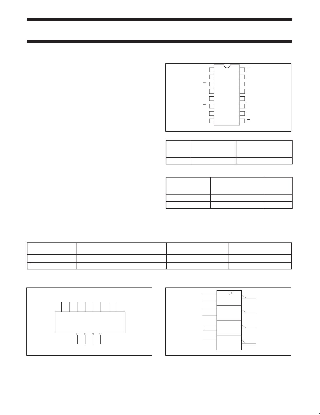
PIN CONFIGURATION
1
D0a
2
D0b
3
Q0
4
GND
5
GND
1
6
Q
D1a
D1b
8
TYPICAL
TYPE
PROPAGATION
DELAY
74F3038 6.0ns 17mA
16
Q3
15
D3b
14
D3a
13
V
CC
V
12
CC
D2a
11
D2b
107
Q
9
2
SF00570
TYPICAL
SUPPLY CURRENT
(TOTAL)
ORDERING INFORMATION
COMMERCIAL RANGE
DESCRIPTION
VCC = 5V ±10%,
T
= 0°C to +70°C
amb
16-pin Plastic DIP N74F3038N SOT38-4
16-pin Plastic SOL N74F3038D SOT162-1
PACKAGE
DRAWING
NUMBER
INPUT AND OUTPUT LOADING AND FAN-OUT TABLE
PINS DESCRIPTION
74F(U.L.)
HIGH/LOW
Dna, Dnb Data inputs 1.0/1.0 20µA/0.6mA
Qn Data outputs OC/266 OC/160mA
NOTE: One (1.0) FAST unit load is defined as: 20µA in the High state and 0.6mA in the Low state. OC = Open Collector.
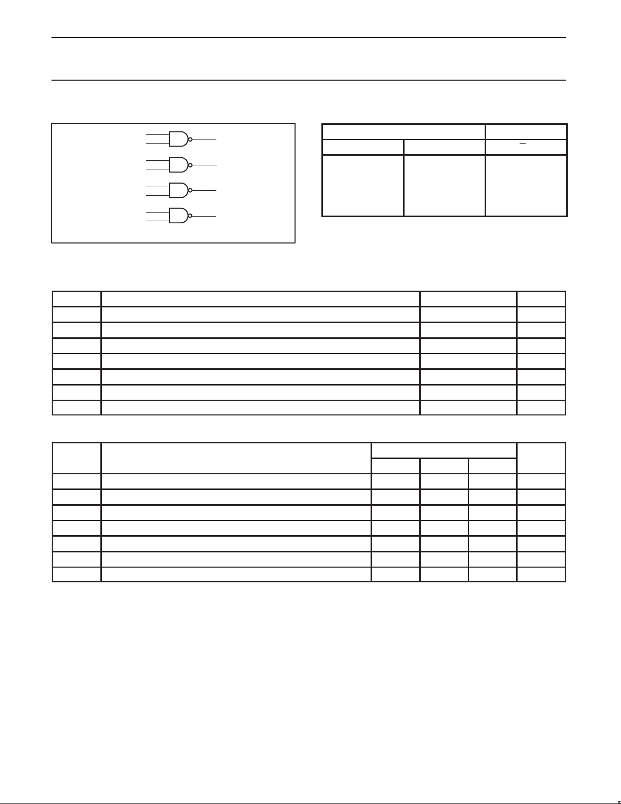
LOGIC SYMBOL
1 2 7 8 10 11 14 15
D0a
VCC = Pin 12,13
GND = Pin 4, 5
D0b D1a D2a D2b D3a D3b
D1a
Q0 Q1 Q2 Q3
36916
SF00571
IEC/IEEE SYMBOL
1
2
7
8
10
11
14
15
&
LOAD VALUE
HIGH/LOW
3
6
9
16
SF00572
1998 May 21 853-0022 19433
2
Philips Semiconductors Product specification
SYMBOL
PARAMETER
UNIT
74F3038Quad 2-input NAND 30Ω line driver (open collector)
LOGIC DIAGRAM
VCC = Pin 12,13
GND = Pin 4, 5
D0a
D0b
D1a
D1b
D2a
D2b
D3a
D3b
1
2
7
8
10
11
14
15
3
6
9
16
SF00569
Q0
Q1
Q2
Q3
FUNCTION TABLE
Dna Dnb Qn
L L H
L H H
H L H
H H L
H = High voltage level
L = Low voltage level
ABSOLUTE MAXIMUM RATINGS
(Operation beyond the limits set forth in this table may impair the useful life of the device.
Unless otherwise noted these limits are over the operating free-air temperature range.)
SYMBOL
V
CC
V
IN
I
IN
V
OUT
I
OUT
T
amb
T
stg
Supply voltage –0.5 to +7.0 V
Input voltage –0.5 to +7.0 V
Input current –30 to +5 mA
Voltage applied to output in High output state –0.5 to V
Current applied to output in Low output state 320 mA
Operating free-air temperature range 0 to +70 °C
Storage temperature range –65 to +150 °C
PARAMETER RA TING UNIT
INPUTS OUTPUT
CC
V
RECOMMENDED OPERATING CONDITIONS
V
V
V
I
V
I
T
CC
IH
IL
IK
OH
OL
amb
Supply voltage 4.5 5.0 5.5 V
High-level input voltage 2.0 V
Low-level input voltage 0.8 V
Input clamp current –18 mA
High-level output voltage 4.5 V
Low-level output current 160 mA
Operating free-air temperature range 0 +70 °C
LIMITS
MIN NOM MAX
1998 May 21
3
 Loading...