

Philips N74F253D, N74F253N Datasheet

INTEGRATED CIRCUITS
74F253
Dual 4-bit input multiplexer (3-State)
Product specification
IC15 Data Handbook
1988 Nov 29

Philips Semiconductors Product specification
74F253Dual 4-input multiplexer (3-State)
FEA TURES
•3-State outputs for bus interface and multiplex expansion
•Common select inputs
•Separate Output Enable Inputs
DESCRIPTION
The 74F253 has two identical 4-input multiplexers with 3-State
outputs which select two bits from four sources selected by common
Select inputs (S0, S1). When the individual Output Enable (OE
b) inputs of the 4-input multiplexers are High, the outputs are
OE
forced to a high impedance (Hi-Z) state.
The 74F253 is the logic implementation of a 2-pole, 4-position
switch; the position of the switch being determined by the logic
levels supplied to the two common Select inputs.
To avoid exceeding the maximum current ratings when the outputs
of the 3-State devices are tied together, all but one device must be
in the high-impedance state. Therefore, only one Output Enable
must be active at a time.
a,
PIN CONFIGURATION
1
a
OE
2
S1
3
I3a
4
I2a
5
I1a
6
I0a
Ya
TYPICAL
TYPE
PROPAGATION
DELAY
74F253 7.0ns 12mA
16
V
CC
15
OE
b
14
S0
13
I3b
I2b
12
I1b
11
107
I0b
98GND Yb
SF00798
TYPICAL
SUPPLY CURRENT
(TOTAL)
ORDERING INFORMATION
COMMERCIAL RANGE
DESCRIPTION
VCC = 5V ±10%,
T
= 0°C to +70°C
amb
16-pin plastic DIP N74F253N SOT38-4
16-pin plastic SO N74F253D SOT109-1
PKG DWG #
INPUT AND OUTPUT LOADING AND FAN-OUT TABLE
PINS DESCRIPTION 74F (U.L.) HIGH/LOW LOAD VALUE HIGH/LOW
I0a–I3a Port A data inputs 1.0/1.0 20µA/0.6mA
I0b–I3b Port B data inputs 1.0/1.0 20µA/0.6mA
S0, S1 Common Select inputs 1.0/1.0 20µA/0.6mA
OEa Port A Output Enable input (active Low) 1.0/1.0 20µA/0.6mA
OEb Port B Output Enable input (active Low) 1.0/1.0 20µA/0.6mA
Ya, Yb 3-State outputs 150/40 3mA/24mA
NOTE:
One (1.0) FAST unit load is defined as: 20µA in the High state and 0.6mA in the Low state.
LOGIC SYMBOL
14
2
1
15
V
= Pin 16
CC
GND = Pin 8
6 13121110
I0a I1a I2a I3a I0b I1b I2b I3b
S0
S1
OEa
OEb
345
Ya Yb
97
SF00799
IEC/IEEE SYMBOL
14
2
1
6
5
4
3
15
10
11
12
13
EN
0
0
G
3
1
MUX
0
1
2
3
7
9
SF00800
1988 Nov 29 853–0101 95206
2
Philips Semiconductors Product specification
74F253Dual 4-input multiplexer (3-State)
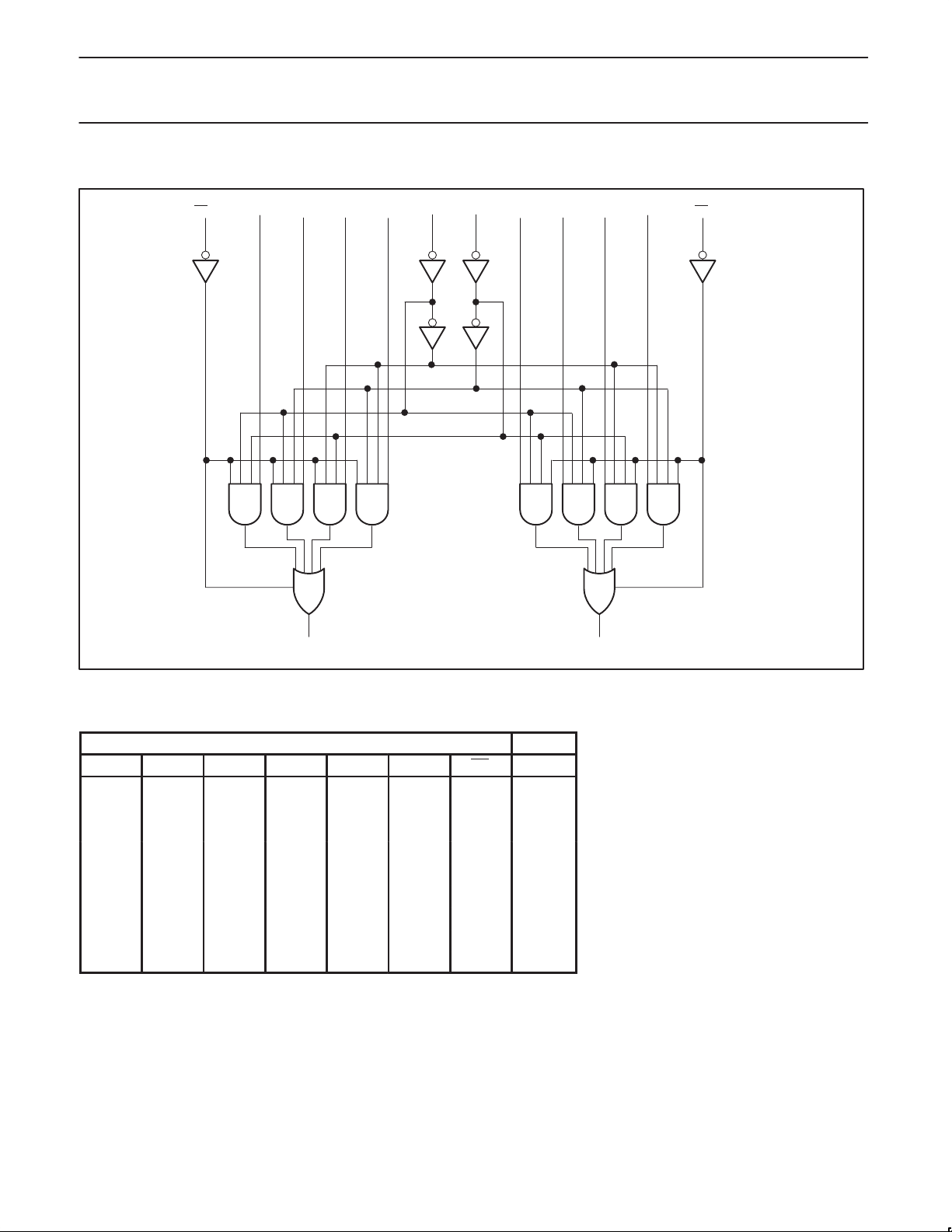
LOGIC DIAGRAM
S0
I0a I1a I2a I3aOE
a
1
S1
3456
2
I0b I1b I2b I3b OE
14
10 11 12 13
b
15
VCC = Pin 16
GND = Pin 8
7
Ya
FUNCTION TABLE
INPUTS OUTPUT
S0 S1 I0 I1 I2 I3 OE Y
X X X X X X H Z
L L L X X X L L
L L H X X X L H
H L X L X X L L
H L X H X X L H
L H X X L X L L
L H X X H X L H
H H X X X L L L
H H X X X H L H
NOTES:
H = High voltage level
L = Low voltage level
X = Don’t care
Z = High impedance “off” state
9
Yb
SF00801
1988 Nov 29
3
 Loading...