

Philips N74F245DB, N74F245D, N74F245N Datasheet

INTEGRATED CIRCUITS
74F245
Octal transceiver (3-State)
Product specification 1994 Nov 15
IC15 Data Handbook
Philips Semiconductors
Philips Semiconductors Product specification
74F245Octal transceiver (3-State)
FEA TURES
•Octal bidirectional bus interface
•3-State buffer outputs sink 64mA
•15mA source current
•Outputs are placed in high impedance state during power-off
conditions
DESCRIPTION
The 74F245 is an octal transceiver featuring non-inverting 3-State
bus compatible outputs in both transmit and receive directions. The
B port outputs are capable of sinking 64mA and sourcing 15mA,
producing very good capacitive drive characteristics. The device
features an Output Enable (OE
Transmit/Receive (T/R
outputs, B0–B7, have been designed to prevent output bus loading if
the power is removed from the device.
TYPE TYPICAL PROPAGATION DELAY TYPICAL SUPPLY CURRENT (TOTAL)
74F245 4.0ns 70mA
ORDERING INFORMATION
DESCRIPTION
20-Pin Plastic DIP N74F245N SOT146-1
20-Pin Plastic SO N74F245D SOT163-1
20-Pin Plastic SSOP Type II N74F245DB SOT339-1
) input for easy cascading and
) input for direction control. The 3-State
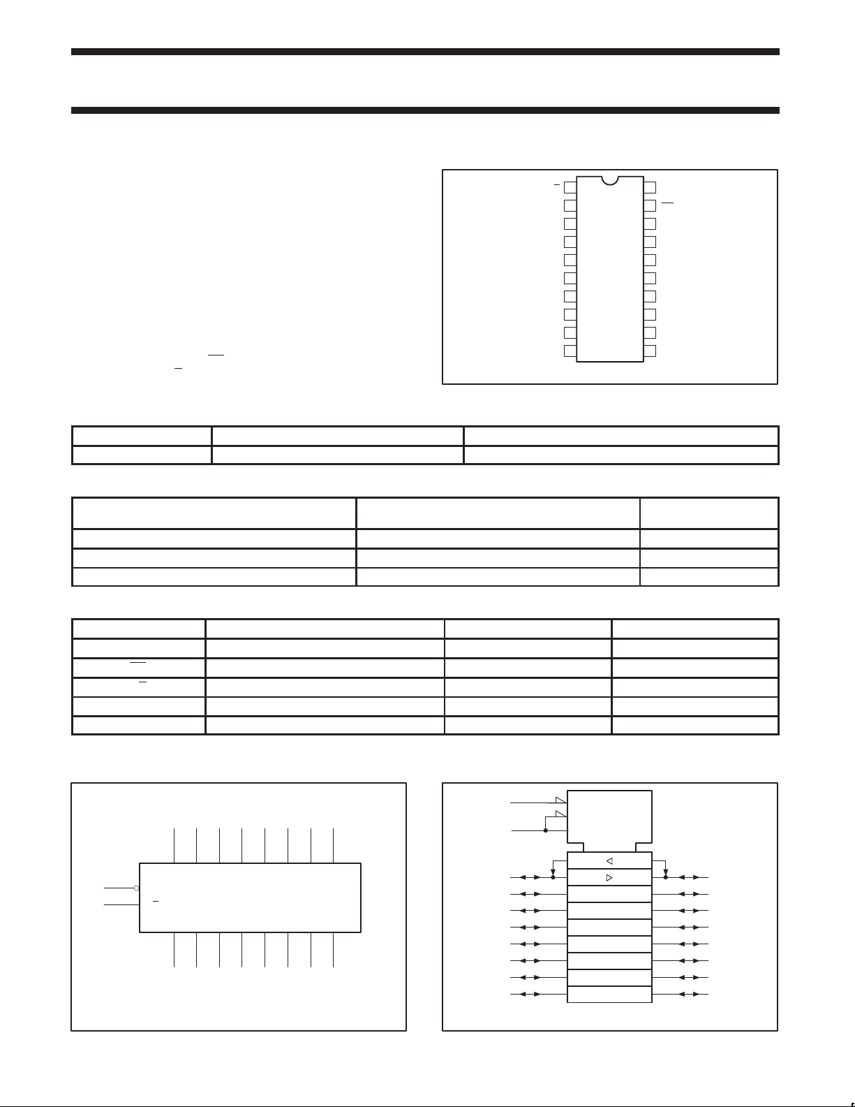
PIN CONFIGURATION
COMMERCIAL RANGE
VCC = 5V ±10%, T
amb
1
T/R
2
A0
3
A1
4
A2
5
A3
6
A4
7
A5
8
A6
9
A7
10 11
GND
= 0°C to +70°C
V
20
CC
19
OE
18
B0
17
B1
16
B2
15
B3
14
B4
13
B5
12
B6
B7
SF00198
DRAWING NUMBER
INPUT AND OUTPUT LOADING AND FAN-OUT TABLE
PINS DESCRIPTION 74F (U.L.) HIGH/LOW LOAD VALUE HIGH/LOW
A0–A7, B0–B7 Data inputs 3.5/1.0 70µA/0.6mA
OE Output Enable input (active Low) 1.0/2.0 20µA/1.2mA
T/R Transmit/Receive input 1.0/2.0 20µA/1.2mA
A0–A7 A port outputs 150/40 3.0mA/24mA
B0–B7 B port outputs 750/106.7 15mA/64mA
NOTE: One (1.0) FAST unit load is defined as: 20µA in the High state and 0.6mA in the Low state.
LOGIC SYMBOL
19
1
V
= Pin 20
CC
GND = Pin 10
OE
T/R
234
A0 A1 A2 A3 A4 A5
B1
B0
17
18
567
B2 B3 B4 B5
16 15 14 13
89
A6 A7
B6 B7
12 11
SF00199
IEC/IEEE SYMBOL
19
1
2
3
4
5
6
7
8
9
G3
3EN1 (BA)
3EN1 (AB)
∇ 1
2 ∇
18
17
16
15
14
13
12
11
SF00200
November 15, 1994 853–0025 14256
2
Philips Semiconductors Product specification
OUTPUTS
I
Current applied to output in Low output state
SYMBOL
PARAMETER
UNIT
IOHHigh-level output current
IOLLow-level output current
74F245Octal transceiver (3-State)
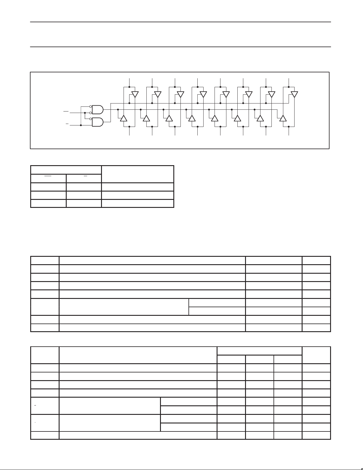
LOGIC DIAGRAM
A0 A1 A2 A3 A4 A5 A6 A7
23456789
19
OE
1
T/R
VCC = Pin 20
GND = Pin 10
FUNCTION TABLE
INPUTS
OE T/R
L L Bus B data to Bus A
L H Bus A data to Bus B
H X Z
H = High voltage level
L = Low voltage level
X = Don’t care
Z = High impedance “off” state
18
B0
17
B1
16
B2
15
B3
14
B4
13
B5
12
B6
B7
SF00201
11
ABSOLUTE MAXIMUM RATINGS
(Operation beyond the limits set forth in this table may impair the useful life of the device.
Unless otherwise noted these limits are over the operating free-air temperature range.)
SYMBOL
V
CC
V
IN
I
IN
V
OUT
OUT
T
amb
T
stg
Supply voltage –0.5 to +7.0 V
Input voltage –0.5 to +7.0 V
Input current –30 to +5 mA
Voltage applied to output in High output state –0.5 to +5.5 V
pp
p
Operating free-air temperature range 0 to +70 °C
Storage temperature range –65 to +150 °C
PARAMETER RATING UNIT
p
A0–A7 48 mA
B0–B7 128 mA
RECOMMENDED OPERATING CONDITIONS
V
V
V
I
T
CC
IH
IL
IK
amb
Supply voltage 4.5 5.0 5.5 V
High-level input voltage 2.0 V
Low-level input voltage 0.8 V
Input clamp current –18 mA
p
p
A0–A7 –3 mA
B0–B7 –15 mA
A0–A7 24 mA
B0–B7 64 mA
Operating free-air temperature range 0 +70 °C
LIMITS
MIN NOM MAX
November 15, 1994
3
 Loading...