

Philips N74F2373N, N74F2373D Datasheet
INTEGRATED CIRCUITS
74F2373
Octal transparent latch with 30Ω
equivalent output termination (3-State)
Product specification
Supersedes data of 1995 Jun 20
IC15 Data Handbook
1999 Feb 01
Philips Semiconductors Product specification
Octal transparent latch with 30Ω equivalent output
termination (3-State)
FEA TURES
•8-bit transparent latch
•30 Ohm output termination for driving DRAM
•3-State outputs glitch free during power-up and power-down
•Common 3-State output register
•Independent register and 3-State buffer operation
DESCRIPTION
The 74F2373 is an octal transparent latch coupled to eight 3-State
output devices. The two sections of the device are controlled
independently by enable (E) and output enable (OE
The 30 Ohm series termination on the outputs reduces
over/undershoot, making them ideal for driving DRAM
ORDERING INFORMATION
DESCRIPTION COMMERCIAL RANGE DRAWING NUMBER
20-pin plastic DIP N74F2373N SOT146-1
20-pin plastic SOL N74F2373D SOT163-1
) control gates.
VCC = 5V ±10%, T
ORDER CODE
The data on the D inputs is transferred to the latch outputs when the
enable (E) input is high. The latch remains transparent to the data
input while E is high, and stores the data that is present one setup
time before the high-to-low enable transition.
The 3-State output buffers are designed to drive heavily loaded
3-State buses, MOS memories, or MOS microprocessors.
The active low output enable (OE
independent of the latch operation. When OE
transparent data appears at the output.
When OE
is high, the outputs are in high impedance “off” state,
which means they will neither drive nor load the bus.
TYPE
74F2373 4.5ns 35mA
= 0°C to +70°C
amb
) controls all eight 3-State buffers
TYPICAL
PROPAGATION
DELA Y
74F2373
is low, latched or
TYPICAL SUPPL Y
CURRENT
(TOTAL)
INPUT AND OUTPUT LOADING AND FAN OUT TABLE
PINS DESCRIPTION
D0 - D7 Data inputs 1.0/1.0
E Enable input (active high) 1.0/1.0
OE Output enable inputs (active low) 1.0/1.0
Q0 - Q7 3-State outputs 150/40 3.0mA/3.0mA
NOTE: One (1.0) FAST unit load is defined as: 20µA in the high state and 0.6mA in the low state.
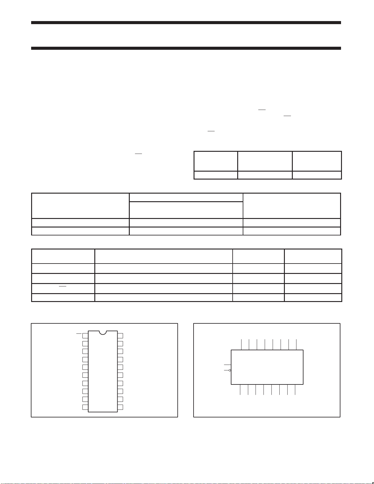
PIN CONFIGURATION
OE
1
2
Q0
3
D0
4
D1
5
Q1
6
Q2
7
D2
8
D3
9
Q3
10 11
GND
20
V
CC
19
Q7
18
D7
17
D6
16
Q6
15
Q5
14
D5
13
D4
12
Q4
E
SF00250
LOGIC SYMBOL
11
E
OE
1
= Pin 20
V
CC
GND = Pin 10
74F (U.L.)
HIGH/LOW
3 4 7 8 13 14 17 18
D0 D1 D2 D3 D4 D5 D6 D7
Q0 Q1 Q2 Q3 Q4 Q5 Q6 Q7
2 5 6 9 12 15 16 19
SF00251
LOAD VALUE
HIGH/LOW
20µA/0.6mA
20µA/0.6mA
20µA/0.6mA
1999 Feb 01 853-2140 20747
2
Philips Semiconductors Product specification
OPERATING MODE
Enable and read register
Latch and read register
Disable outputs
Octal transparent latch with 30Ω equivalent output
termination (3-State)
IEC/IEEE SYMBOL
1
11
3
4
7
8
13
14
17
18
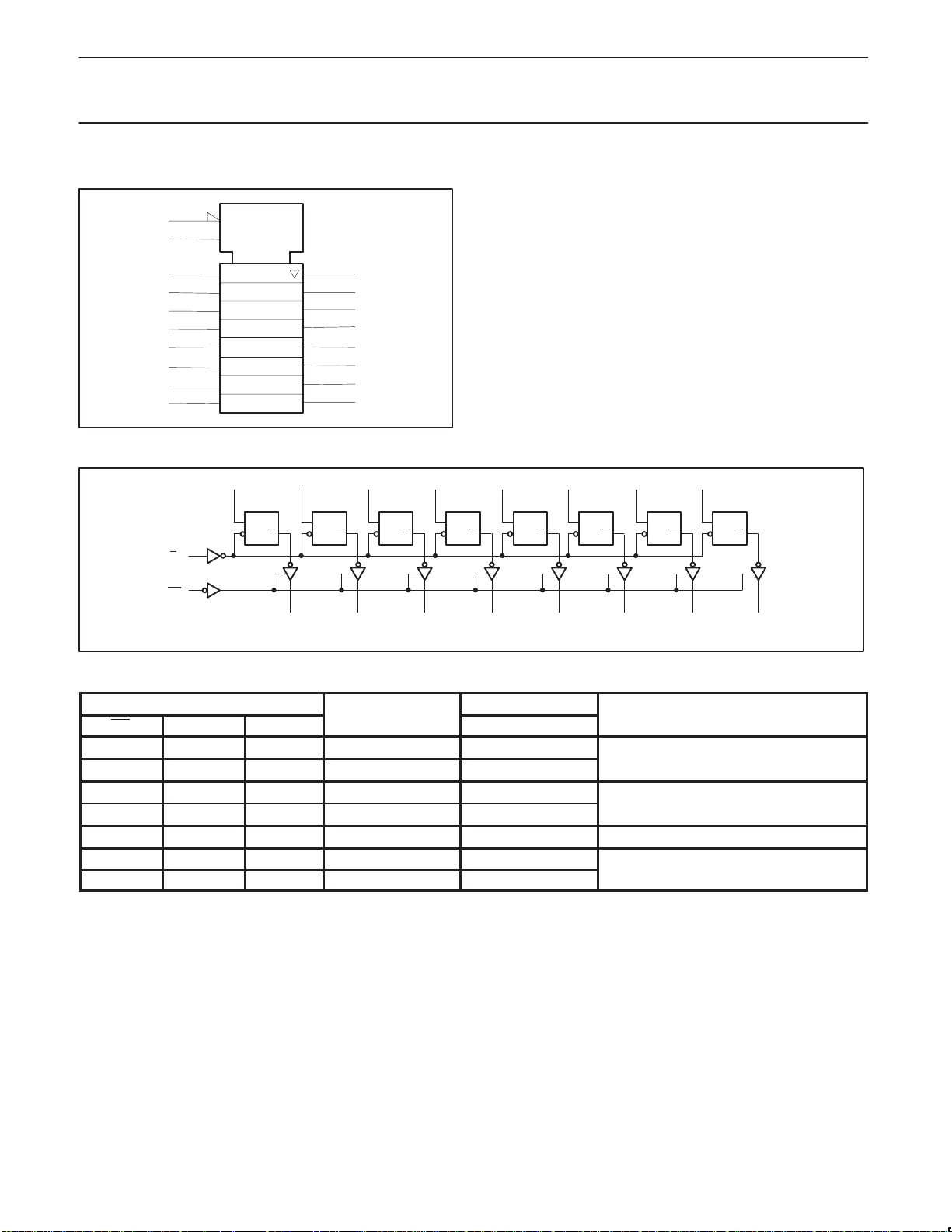
LOGIC DIAGRAM
E
EN1
EN2
SF00252
4
D
E
2
5
6
9
12
15
16
19
D2
7
Q
D
E
D3
8
Q
D
E
D4
13
Q
D
E
2D
D0
11
1
3
D
E
D1
Q
74F2373
D5
14
D
Q
E
D6
17
Q
E
D7
18
D
D
Q
Q
E
1
V
= Pin 20
CC
GND = Pin 10
OE
Q0
2
Q1
5
Q2
6
Q3
9
Q4
FUNCTION TABLE
INPUTS
OE E Dn
INTERNAL
REGISTER
L H L L L
L H H H H
L ↓ l L L
L ↓ h H H
L L X NC NC Hold
H L X NC Z
H H Dn Dn Z
NOTES:
H = High-voltage level
h = High state must be present one setup time before the high-to-low enable transition
L = Low-voltage level
l = Low state must be present one setup time before the high-to-low enable transition
NC= No change
X = Don’t care
Z = High impedance “off” state
↓ = High-to-low enable transition
OUTPUTS
Q0 - Q7
12
Q5
15
Q6
16
19
Q7
SF00256
p
1999 Feb 01
3
 Loading...