

Philips N74F219AN, N74F219AD Datasheet
INTEGRATED CIRCUITS
74F219A
64-bit TTL bipolar RAM, non-inverting
(3-State)
Product specification 1996 Jan 05
IC15 Data Handbook
Philips Semiconductors Product specification
74F219A64-bit TTL bipolar RAM, non-inverting (3-State)
FEA TURES
•High speed performance
•Replaces 74F219
•Address access time: 8ns max vs 28ns for 74F219
•Power dissipation: 4.3mW/bit typ
•Schottky clamp TTL
•One chip enable
•Non–Inverting outputs (for inverting outputs see 74F189A)
•3–state outputs
•74F219A in 150 mil wide SO is preferred options for new designs
•C3F219A in 300 mil wide SOL replaces 74F219 in existing
designs
DESCRIPTION
The 74F219A is a high speed, 64–bit RAM organized as a 16–word
by 4–bit array. Address inputs are buf fered to minimize loading and
are fully decoded on chip. The outputs are in high impedance state
whenever the chip enable (CE) is high. The outputs are active only
in the READ mode (WE
complement of the stored data.
TYPE TYPICAL ACCESS TIME TYPICAL SUPPL Y CURRENT(TOTAL)
74F219A 5.0ns 55mA
= high) and the output data is the
APPLICATIONS
•Scratch pad memory
•Buffer memory
•Push down stacks
•Control store
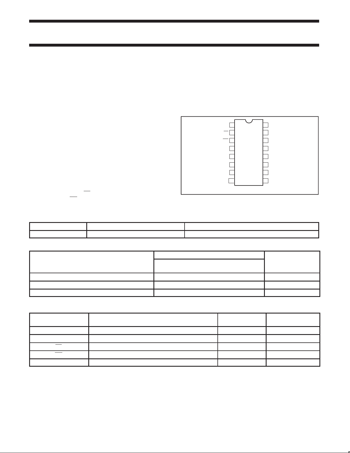
PIN CONFIGURATION
1
A0
2
CE
WE
3
4
D0
Q0
5
D1
6
Q1
GND
16
V
A1
15
A2
14
13
A3
D3
12
11
Q3
D2
107
Q2
98
SF00307
CC
ORDERING INFORMATION
ORDER CODE
DESCRIPTION COMMERCIAL RANGE
= 5V ±10%, T
V
CC
16-pin plastic Dual In-line Package N74F219AN SOT38-4
16-pin plastic Small Outline (150mil) N74F219AD SOT109-1
16-pin plastic Small Outline Large (300mil) C3F219AD SOT162–1
= 0°C to +70°C
amb
DRAWING NUMBER
INPUT AND OUTPUT LOADING AND FAN OUT TABLE
PINS DESCRIPTION 74F (U.L.)
HIGH/LOW
D0 – D3 Data inputs 1.0/1.0 20µA/0.6mA
A0 – A3 Address inputs 1.0/1.0 20µA/0.6mA
CE Chip enable input (active low) 1.0/2.0 20µA/1.2mA
WE Write enable input (active low) 1.0/2.0 20µA/1.2mA
Q0 – Q3 Data outputs 150/40 3mA/24mA
NOTE: One (1.0) FAST unit load is defined as: 20µA in the high state and 0.6mA in the low state.
LOAD VALUE
HIGH/LOW
1996 Jan 05 853-1308 16196
2
Philips Semiconductors Product specification
74F219A64-bit TTL bipolar RAM, non-inverting (3-State)
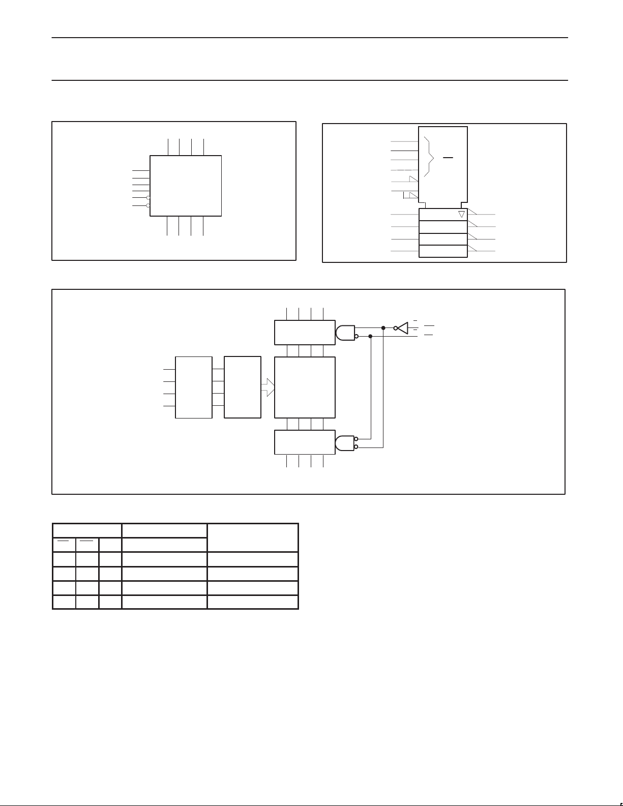
LOGIC SYMBOL
1
15
14
13
2
3
VCC = pin 16
GND = pin 8
LOGIC DIAGRAM
4
D0 D2 D3D1
A0
A1
A2
A3
CE
WE
Q0 Q1 Q2 Q3
57911
1
A0
15
A1
14
A2
13
A3
61012
SF00308
Decoder
Drivers
Address
Decoder
D0 D1 D2 D3
4 6 10 12
Data buffers
16–word x 4–bit
memory cell
array
IEC/IEEE SYMBOL
1
15
14
13
2
3
4
6
10
12
RAM 16X4
0
1
G1
1 EN [READ]
1 C2 [WRITE]
A,2D A
3
WE
2
CE
0
A
15
5
7
9
11
SF00301
VCC = Pin 16
GND = Pin 8
FUNCTION TABLE
INPUTS OUTPUT OPERATING
CE WE Dn Q
n
L H X Stored data Read
L L L High impedance Write “0”
L L H High impedance Write “1”
H X X High impedance Disable input
NOTES:
H = High voltage level
L = Low voltage level
X = Don’t care
MODE
Output buffers
57911
Q0 Q1 Q2 Q3
SF00309
1996 Jan 05
3

Philips Semiconductors Product specification
SYMBOL
PARAMETER
UNIT
74F219A64-bit TTL bipolar RAM, non-inverting (3-State)
ABSOLUTE MAXIMUM RATINGS
(Operation beyond the limit set forth in this table may impair the useful life of the device.
Unless otherwise noted these limits are over the operating free-air temperature range.)
SYMBOL
V
V
I
IN
V
I
OUT
T
amb
T
stg
CC
IN
OUT
Supply voltage –0.5 to +7.0 V
Input voltage –0.5 to +7.0 V
Input current –30 to +5 mA
Voltage applied to output in high output state –0.5 to V
Current applied to output in low output state 48 mA
Operating free-air temperature range 0 to +70 °C
Storage temperature range –65 to +150 °C
RECOMMENDED OPERATING CONDITIONS
V
V
V
I
I
I
T
CC
IH
IL
Ik
OH
OL
amb
Supply voltage 4.5 5.0 5.5 V
High–level input voltage 2.0 V
Low–level input voltage 0.8 V
Input clamp current –18 mA
High–level output current –3 mA
Low–level output current 24 mA
Operating free-air temperature range 0 +70 °C
PARAMETER RATING UNIT
CC
V
LIMITS
MIN NOM MAX
DC ELECTRICAL CHARACTERISTICS
(Over recommended operating free-air temperature range unless otherwise noted.)
SYMBOL
V
OH
High-level output voltage VCC = MIN, VIL = MAX
PARAMETER TEST CONDITIONS
VIH = MIN, IOH = MAX
V
OL
V
IK
I
I
I
IH
I
IL
Low-level output voltage VCC = MIN, VIL = MAX
VIH = MIN, I
Input clamp voltage VCC = MIN, II = I
OL
= MAX
IK
Input current at maximum input voltage VCC = MAX, VI = 7.0V 100 µA
High–level input current VCC = MAX, VI = 2.7V 20 µA
Low–level input current others VCC = MAX, VI = 0.5V -0.6 mA
CE, WE -1.2 mA
I
OZH
I
OZL
I
OS
I
CC
C
C
IN
OUT
Offset output current,
high–level voltage applied
Offset output current,
low–level voltage applied
Short-circuit output current
3
VCC = MAX, VI = 2.7V 50
VCC = MAX, VI = 0.5V –50
VCC = MAX -60 -150 mA
Supply current (total) VCC = MAX, CE = WE = GND 55 80 mA
Input capacitance VCC = 5V, VIN = 2.0V 4 pF
Output capacitance VCC = 5V, V
= 2.0V 7 pF
OUT
NOTES:
1. For conditions shown as MIN or MAX, use the appropriate value specified under recommended operating conditions for the applicable type.
2. All typical values are at V
3. Not more than one output should be shorted at a time. For testing I
techniques are preferable in order to minimize internal heating and more accurately reflect operational values. Otherwise, prolonged shorting
CC
= 5V, T
amb
= 25°C.
, the use of high-speed test apparatus and/or sample-and-hold
OS
of a high output may raise the chip temperature well above normal and thereby cause invalid readings in other parameter tests. In any
sequence of parameter tests, I
tests should be performed last.
OS
1
±10%V
±10%V
±5%V
±5%V
CC
CC
CC
CC
LIMITS UNIT
MIN TYP
2
MAX
2.4 V
2.7 3.4 V
0.35 0.50 V
0.35 0.50 V
-0.73 -1.2 V
µA
µA
1996 Jan 05
4
 Loading...