

Philips N74F198N, N74F198D Datasheet

INTEGRATED CIRCUITS
74F198
8-bit bidirectional universal shift register
Product specification
IC15 Data Handbook
1987 Oct 02
Philips Semiconductors Product specification
74F1988-bit bidirectional universal shift register
FEA TURES
•Buffered clock and control inputs
•Shift right, shift left, and parallel load capability
•Asynchronous Master Reset
DESCRIPTION
The 74F198 Bidirectional Universal Shift Register is designed to
incorporate virtually all of the features a system designer may want
in a shift register. This circuit features parallel inputs and outputs,
shift right and shift left serial inputs, operating mode select inputs,
and direct overriding master reset input. The register has four
distinct modes of operation:
– Parallel (broadside) load
– Shift right (in the direction Q0 toward Q7)
– Shift left (in the direction Q7 toward Q0)
– Inhibit clock (do nothing).
Synchronous parallel loading is accomplished by applying the 8 bits
of data and taking both mode control inputs, S0 and S1, High. The
data is loaded into the associated flip-flop and appears at the
outputs after the positive transition of the clock inputs. During
loading, serial data flow is inhibited.
Shift right is accomplished synchronously, with the rising edge of the
clock pulse when S0 is High and S1 is Low. Serial data for this
mode is entered at the right data input (D
S1 is High, data shifts left synchronously and new data is entered at
the shift-left serial input (D
SL
).
Clocking of the flip-flops is inhibited when both mode control inputs
are Low.
). When S0 is Low and
SR
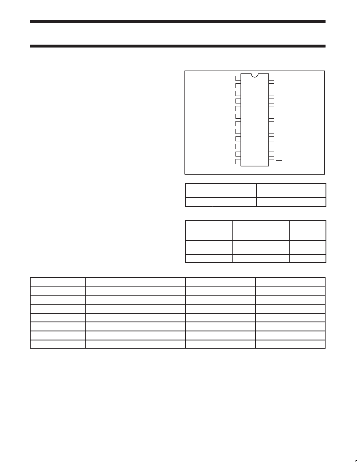
PIN CONFIGURATION
1
S0
2
D
SR
3
D0
4
Q0
5
D1
6
Q1
7
D2
8
Q2
9
D3
10
Q3
11
CP
12 13
GND
TYPE TYPICAL f
TYPICAL SUPPL Y CURRENT
MAX
74F198 95MHz 73mA
24
23
22
21
20
19
18
17
16
15
14
SF00160
V
CC
S1
D
SL
D7
Q7
D6
Q6
D5
Q5
D4
Q4
MR
(TOTAL)
ORDERING INFORMATION
COMMERCIAL RANGE
DESCRIPTION
24-pin Plastic Slim
DIP (300mil)
24-pin Plastic SOL N74F198D SOT137-1
VCC = 5V ±10%,
T
= 0°C to +70°C
amb
N74F198N SOT222-1
PKG DWG #
INPUT AND OUTPUT LOADING AND FAN-OUT TABLE
PINS DESCRIPTION 74F (U.L.) HIGH/LOW LOAD VALUE HIGH/LOW
D0–D7 Parallel data inputs 1.0/1.0 20µA/0.6mA
D
SR
D
SL
S0–S1 Mode Select inputs 1.0/1.0 20µA/0.6mA
CP Clock Pulse input (Active rising edge) 1.0/1.0 20µA/0.6mA
MR Master Reset input (Active Low) 1.0/1.0 20µA/0.6mA
Q0–Q7 Data outputs 50/33 1.0mA/20mA
NOTE: One (1.0) FAST unit load is defined as: 20µA in the High state and 0.6mA in the Low state.
Serial data input (Shift Right) 1.0/1.0 20µA/0.6mA
Serial data input (Shift Left) 1.0/1.0 20µA/0.6mA
October 2, 1987 853–0089 90746
2
Philips Semiconductors Product specification
MR
CP
Q0
Q1…Q6
Q7
74F1988-bit bidirectional universal shift register
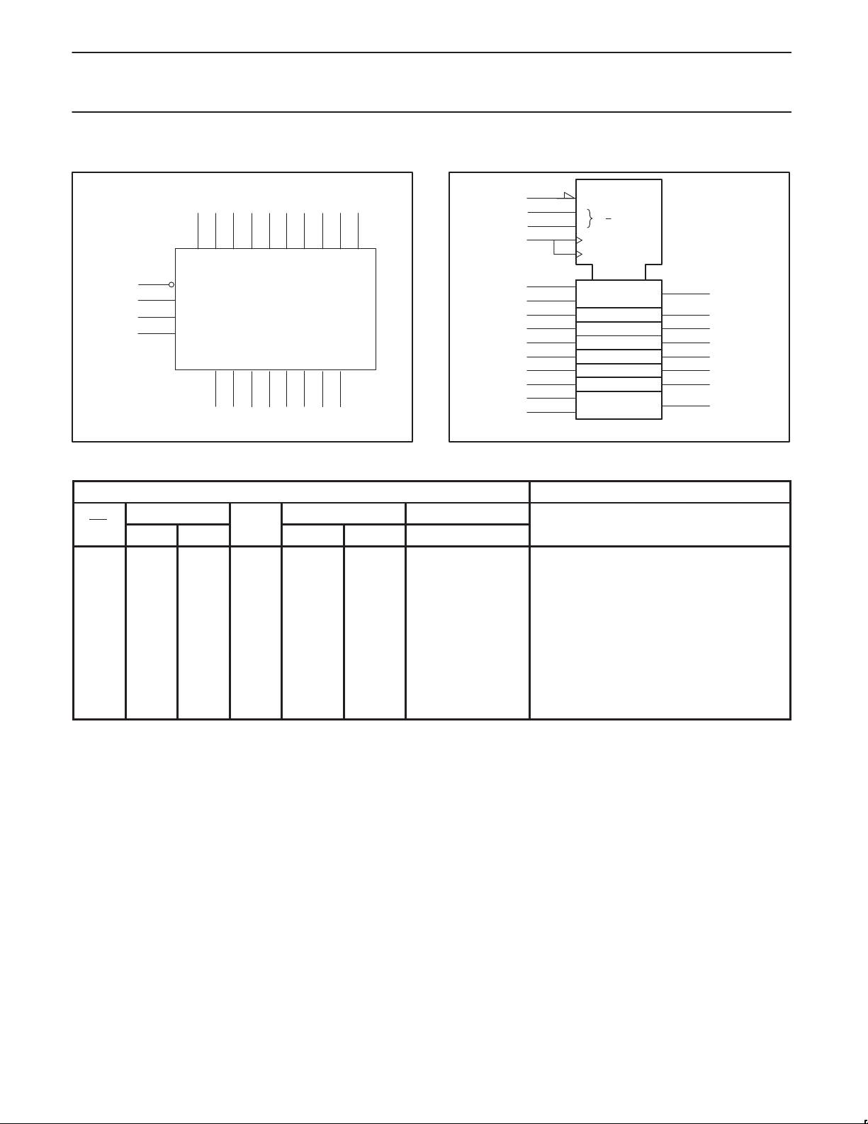
LOGIC SYMBOL
13
1
23
11
= Pin 24
V
CC
GND = Pin 12
79
35
222
D1 D2
D3D0
MR
S0
S1
CP
D
SR
Q0 Q1 Q2 Q3
46810
19 21
15 17
D5 D6
Q5 Q6 Q7
Q4
14 16 18 20
D7D4
D
SF00161
SL
IEC/IEEE SYMBOL
13
1
23
11
2
3
5
7
9
15
17
19
21
22
R
0
M
1
C4
1 → /2 ←
1, 4D
3, 4D
3, 4D
3, 4D
2, 4D
SRG8
0
3
4
6
8
10
14
16
18
20
SF00162
FUNCTION TABLE
INPUTS OUTPUTS
MODE
S0 S1
L X X X X X X L L L L
H X X L X X X Q00 Q10 Q60 Q70
H H H ↑ X X 0…7 0 167
H H L ↑ X H X H Q0n Q5n Q6n
H H L ↑ X L X L Q0n Q5n Q6n
H L H ↑ H X X Q1n Q2n Q7n H
H L H ↑ L X X Q1n Q2n Q7n L
H L L X X X X Q00 Q10 Q60 Q70
H = High voltage level
L = Low voltage level
X = Don’t care
↑ = Low-to-High transition of designated input
0…7 = The level of steady input at inputs 0 through 7, respectively.
Q00, Q10, Q60, Q70 = The level of Q0, Q1, Q6, Q7, respectively, before the indicated steady state input conditions were established.
Q0n, Q1n, Q6n, Q7n = The level of Q0, Q1, Q6, Q7, respectively, before the most recent Low-to-High clock transition.
SERIAL PARALLEL
LEFT RIGHT 0…7
October 2, 1987
3
Philips Semiconductors Product specification
74F1988-bit bidirectional universal shift register
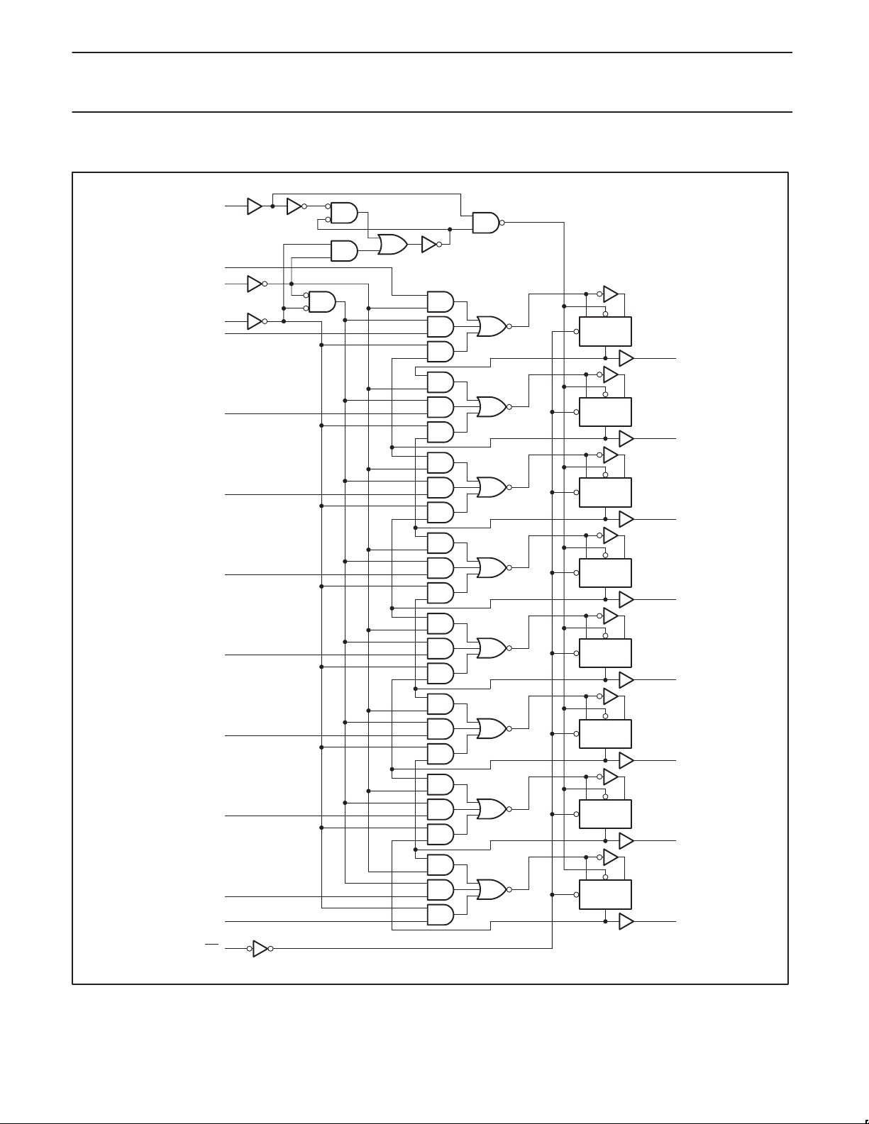
LOGIC DIAGRAM
11
CP
2
D
SR
23
S1
1
S0
3
D0
RCPS
Q
4
Q0
5
D1
7
D2
9
D3
15
D4
17
D5
19
D6
RCPS
Q
RCPS
Q
RCPS
Q
RCPS
Q
RCPS
Q
RCPS
Q
6
Q1
8
Q2
10
Q3
14
Q4
16
Q5
18
Q6
October 2, 1987
D
MR
21
D7
22
SL
13
RCPS
Q
20
SF00163
Q7
4
 Loading...