

Philips N74F194D, N74F194N Datasheet

INTEGRATED CIRCUITS
74F194
4-bit bidirectional universal shift register
Product specification
IC15 Data Handbook
1989 Apr 04
Philips Semiconductors Product specification
74F1944-bit bidirectional universal shift register
FEA TURES
•Shift right and shift left capability
•Synchronous parallel and serial data transfer
•Easily expanded for both serial and parallel operation
•Asynchronous Master Reset
•Hold (do nothing) mode
DESCRIPTION
The functional characteristics of the 74F194 4-Bit Bidirectional Shift
Register are indicated in the Logic Diagram and Function Table. The
register is fully synchronous, with all operations taking place in less
than 9ns (typical) for 74F, making the device especially useful for
implementing very high speed CPUs, or for memory buffer registers.
The 74F194 design has special logic features which increase the
range of application. The synchronous operation of the device is
determined by two Mode Select inputs, S0 and S1. As shown in the
Mode Select-Function Table, data can be entered and shifted from
left to right (shift right, Q0→Q1, etc.), or right to left (shift left,
Q3→Q2, etc.), or parallel data can be entered, loading all 4 bits of
the register simultaneously. When both S0 and S1 are Low, existing
data is retained in a hold (do nothing) mode. The first and last
stages provide D-type Serial Data inputs (D
multistage shift right or shift left data transfers without interfering
with parallel load operation. Mode Select and data inputs on the
74F194 are edge-triggered, responding only to the Low-to-High
transition of the Clock (CP). Therefore, the only timing restriction is
that the Mode Select and selected data inputs must be stable one
setup time prior to the Low-to-High transition of the clock pulse.
Signals on the Mode Select, Parallel Data (D0–D3) and Serial Data
(D
, DSL) can change when the clock is in either state, provided
SR
only the recommended setup and hold times, with respect to the
clock rising edge, are observed. The four Parallel Data inputs
(D0–D3) are D-type inputs. Data appearing on (D0–D3) inputs when
S0 and S1 are High is transferred to the Q0–Q3 outputs
respectively, following the next Low-to-High transition of the clock.
When Low, the asynchronous Master Reset (MR
input conditions and forces the Q outputs Low.
, DSL) to allow
SR
) overrides all other
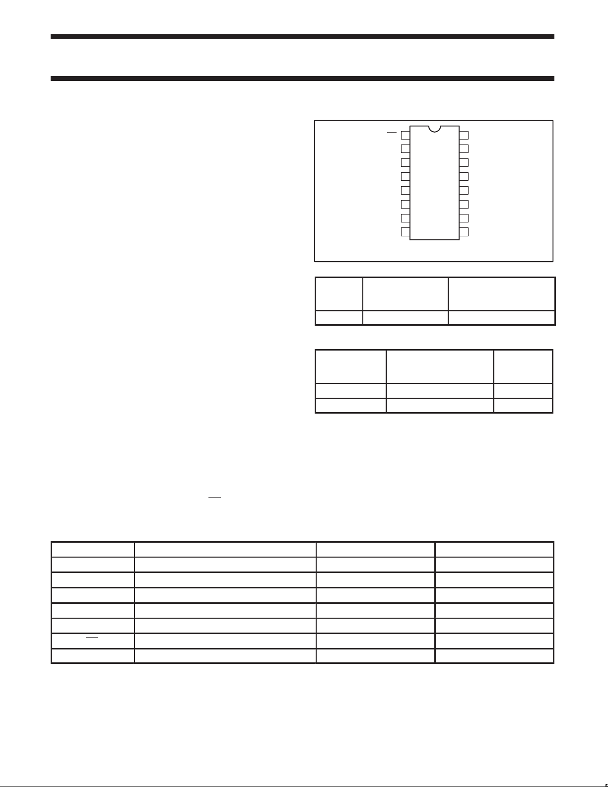
PIN CONFIGURATION
MR
1
D
2
SR
D0
3
D1
4
D2
5
D3
6
D
SL
TYPE TYPICAL f
MAX
74F194 150MHz 33mA
16
V
CC
Q0
15
Q1
14
Q2
13
Q3
12
CP
11
S1
107
98GND S0
SF00167
TYPICAL
SUPPLY CURRENT
(TOTAL)
ORDERING INFORMATION
COMMERCIAL RANGE
DESCRIPTION
16-pin plastic DIP N74F194N SOT38-4
16-pin plastic SO N74F194D SOT109-1
VCC = 5V ±10%,
T
= 0°C to +70°C
amb
PKG DWG #
INPUT AND OUTPUT LOADING AND FAN-OUT TABLE
PINS DESCRIPTION 74F (U.L.) HIGH/LOW LOAD VALUE HIGH/LOW
D0–D3 Parallel data inputs 1.0/1.0 20µA/0.6mA
D
SR
D
SL
S0, S1 Mode Select inputs 1.0/1.0 20µA/0.6mA
CP Clock Pulse input (active rising edge) 1.0/1.0 20µA/0.6mA
MR Asynchronous master Reset input (Active Low) 1.0/1.0 20µA/0.6mA
Q0–Q3 Data outputs 50/33 1.0mA/20mA
NOTE: One (1.0) FAST unit load is defined as: 20µA in the High state and 0.6mA in the Low state.
April 4, 1989 853–0354 96224
Serial data input (Shift Right) 1.0/1.0 20µA/0.6mA
Serial data input (Shift Left) 1.0/1.0 20µA/0.6mA
2
Philips Semiconductors Product specification
74F1944-bit bidirectional universal shift register
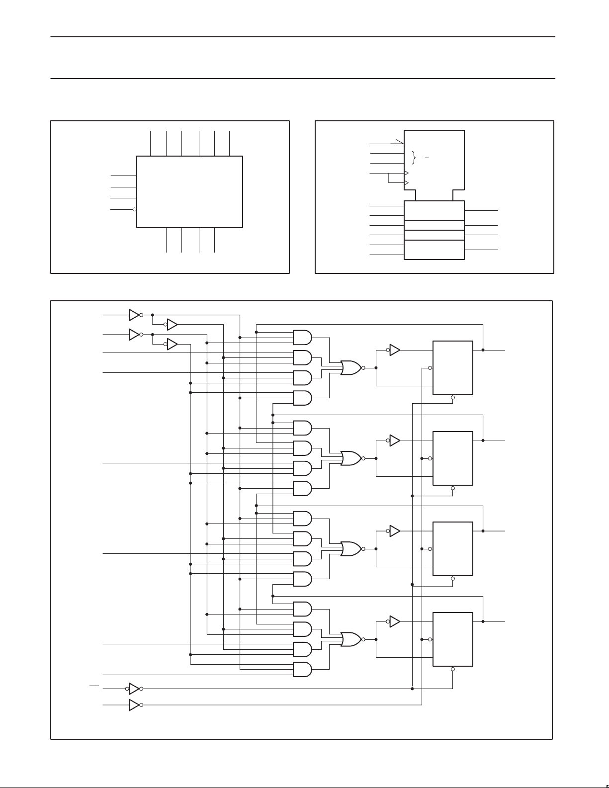
LOGIC SYMBOL
9
10
11
1
V
= Pin 24
CC
GND = Pin 12
LOGIC DIAGRAM
10
S1
9
S0
7
D
SL
6
D3
S0
S1
CP
MR
D
2
SR
34
D1 D2
Q0 Q1
15 14
56
D3D0
Q2 Q3
13 12
7
D
SL
SF00168
IEC/IEEE SYMBOL
1
9
10
11
2
3
4
5
6
7
R
0
M
1
C4
1 → /2 ←
1, 4D
3, 4D
3, 4D
3, 4D
3, 4D
2, 4D
SRG8
0
3
S
CP
R
15
14
13
12
SF00169
Q3
R
D
12
Q3
D
MR
VCC = Pin 24
GND = Pin 12
CP
13
14
15
SF00170
Q2
Q1
Q0
S
Q2
5
D2
4
D1
3
D0
2
SR
1
11
CP
R
S
CP
R
S
CP
R
R
D
Q1
R
D
Q0
R
D
April 4, 1989
3
 Loading...