

Philips N74F191N, N74F191D Datasheet

INTEGRATED CIRCUITS
74F191
Up/down binary counter with reset and
ripple clock
Product specification
IC15 Data Handbook
1995 Jul 17
Philips Semiconductors Product specification
74F191Up/Down binary counter with reset and ripple clock
FEA TURES
•High speed –125MHz typical f
MAX
•Synchronous, reversible counting
•4-Bit binary
•Asynchronous parallel load capability
•Cascadable without external logic
•Single up/down control input
DESCRIPTION
The 74F191 is a 4-bit binary counter. It contains four edge-triggered
master/slave flip-flops with internal gating and steering logic to
provide asynchronous preset and synchronous count-up and
count-down operations.
Asynchronous parallel load capability permits the counter to be
preset to any desired number. Information present on the parallel
data inputs (D
outputs when the Parallel Load (PL
overrides the counting function. Counting is inhibited by a High level
on the count enable (CE) input. When CE is Low, internal state
changes are initiated. Overflow/underflow indications are provided
by two types of outputs, the Terminal Count (TC) and Ripple Clock
(RC
).
The TC output is normally Low and goes High when: 1) the count
reaches zero in the countdown mode or 2) reaches “15” in the count
up mode. The TC output will remain High until a state change
occurs, either by counting or presetting, or until U
output should not be used as a clock signal because it is subject to
decoding spikes. The TC signal is used internally to enable the RC
output. When TC is High and CE is Low, the RC follows the clock
pulse. The RC
width, although delayed in time by two gate delays.
- D3) is loaded into the counter and appears on the
0
) input is Low. This operation
/D is changed. TC
output essentially duplicates the Low clock pulse
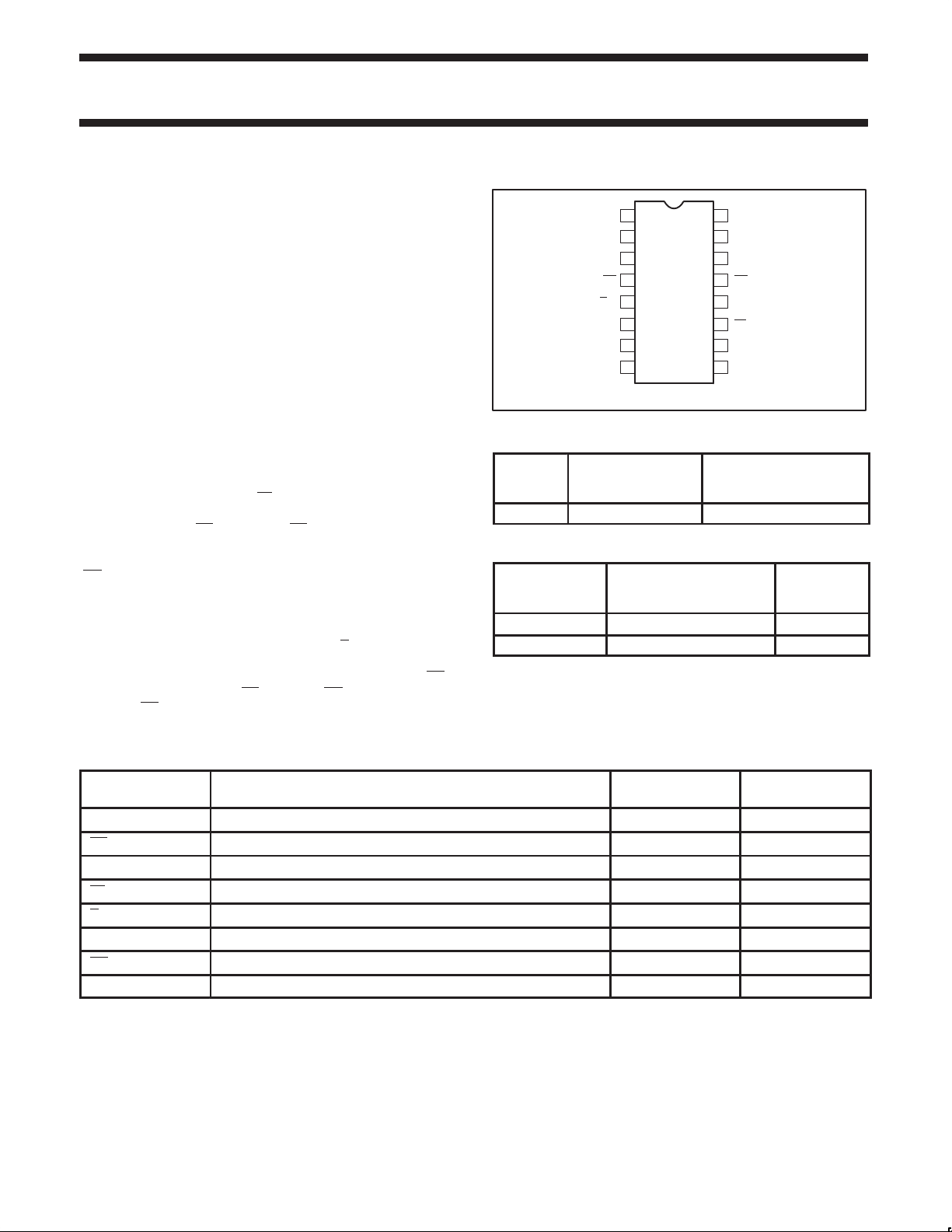
PIN CONFIGURATION
1
D
1
2
Q
1
3
Q
0
CE
4
U/D
5
6
Q
2
7
Q
3
GND
TYPE TYPICAL f
MAX
74F191 125MHz 40mA
16
V
CC
15
D
0
CP
14
RC
13
TC
12
PL
11
10
D
2
98
D
3
SF00729
TYPICAL
SUPPLY CURRENT
(TOTAL)
ORDERING INFORMATION
COMMERCIAL RANGE
DESCRIPTION
16-pin plastic DIP N74F191N SOT38-4
16-pin plastic SO N74F191D SOT109-1
VCC = 5V ±10%,
T
= 0°C to +70°C
amb
PKG DWG #
INPUT AND OUTPUT LOADING AND FAN-OUT TABLE
PINS DESCRIPTION
D0 - D
3
Data inputs 1.0/1.0 20µA/0.6mA
74F(U.L.)
HIGH/LOW
CE Count enable input (active Low) 1.0/3.0 20µA/1.8mA
CP Clock pulse input (active rising edge) 1.0/1.0 20µA/0.6mA
PL Asynchronous parallel load control input (active Low) 1.0/1.0 20µA/0.6mA
U/D Up/down count control input 1.0/1.0 20µA/0.6mA
Q0 - Q
3
Flip-flop outputs 50/33 1.0mA/20mA
RC Ripple clock output (active low) 50/33 1.0mA/20mA
TC Terminal count output 50/33 1.0mA/20mA
NOTE: One (1.0) FAST Unit Load (U.L.) is defined as: 20µA in the High state and 0.6mA in the Low state.
1995 Jul 17 853–0352 15459
2
LOAD VALUE
HIGH/LOW
Philips Semiconductors Product specification
74F191Up/Down binary counter with reset and ripple clock
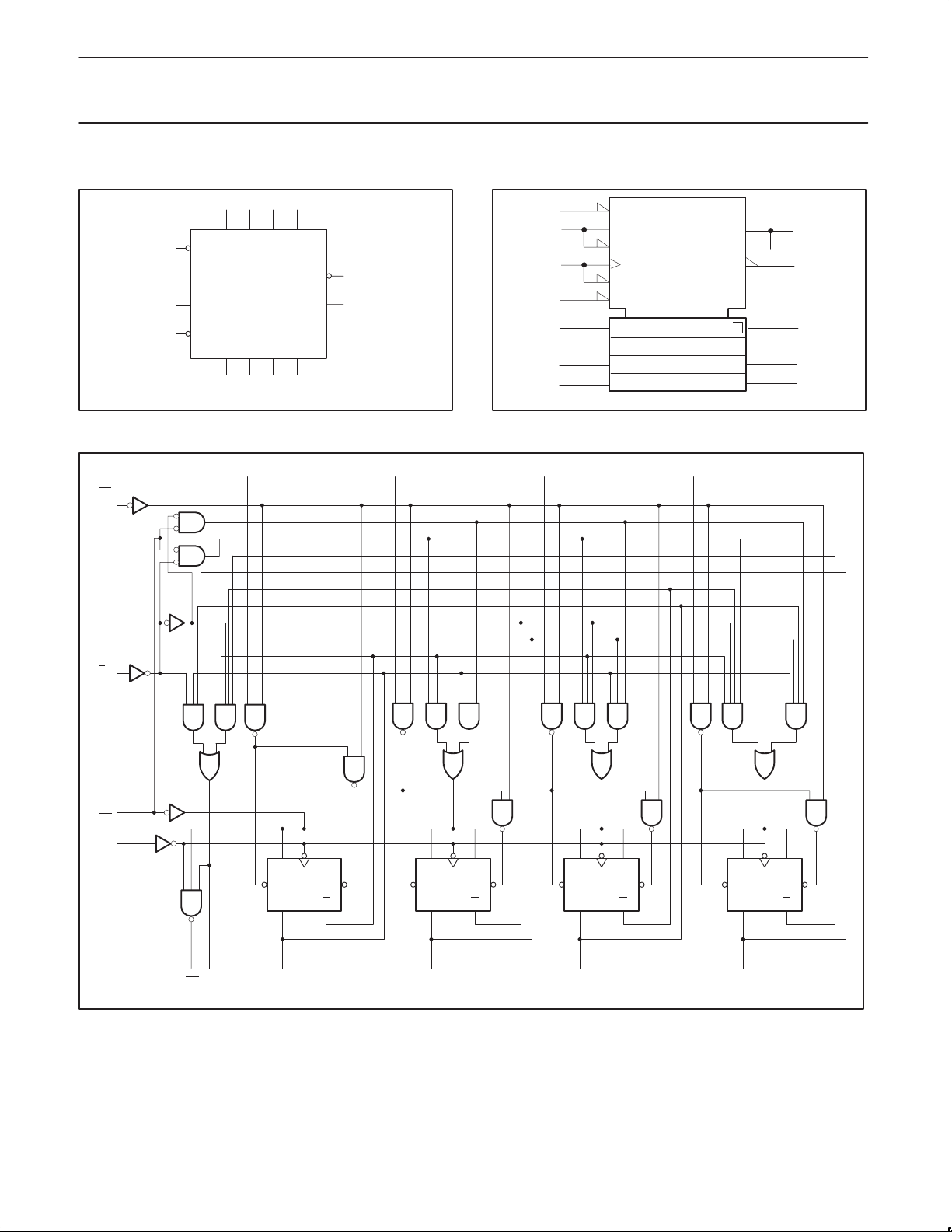
LOGIC SYMBOL
4
5
14
11
VCC=Pin 16
GND=Pin 8
LOGIC DIAGRAM
PL
11
15 1 10 9
D0D
CE
/D
U
CP
PL
Q
0
LOGIC SYMBOL (IEEE/IEC)
4
5
D
D
1
2
3
13
RC
12
TC
Q
Q2Q
1
3
7623
14
11
15
1
10
9
SF00730
D
0
15 1 10 9
D
1
D
2
EN1
M2[DOWN]
M3[UP]
1,2–/1,3+
G4
C5 [LOAD]
5D
CTR DIV 10
[1]
[2]
[4]
[8]
2(CT=0)Z6
3(CT=15)Z6
6, 4, 1
+ –
D
3
12
13
3
2
6
7
SF00731
5
U/D
4
CE
14
CP
VCC= Pin 16
GND = Pin 8
KJ
CP
S
TCRC
Q
R
D
Q
0
D
Q
S
KJ
CP
R
D
Q
Q
1
D
Q
S
KJ
CP
R
D
Q
Q
2
D
Q
S
KJ
CP
R
D
Q
Q
3
D
Q
76231213
SF00732
1995 Jul 17
3
Philips Semiconductors Product specification
74F191Up/Down binary counter with reset and ripple clock
MODE SELECT — FUNCTION TABLE
INPUTS OUTPUTS OPERATING MODE
PL U/D CE CP D
L
L
H L l ↑ X Count up Count up
H H l ↑ X Count down Count down
H X H X X No change Hold (do nothing)
X
X
X
X
X
X
n
L
H
TC AND RC FUNCTION T ABLE
INPUTS TERMINAL COUNT STATE OUTPUTS
U/D CE CP Q
H H X H H H H L H
L H X H H H H H H
L L H H H H H
L H X L L L L L H
H H X L L L L H H
H L L L L L H
H = High voltage level steady state
L = Low voltage level steady state
X = Don’t care
= Low pulse
↑ = Low-to-High clock transition
l = Low voltage level one set-up time prior to the Low-to-High clock transition
0
Q
1
Q
n
L
H
Q
2
Parallel load
Q
3
TC RC
1995 Jul 17
4
Philips Semiconductors Product specification
74F191Up/Down binary counter with reset and ripple clock
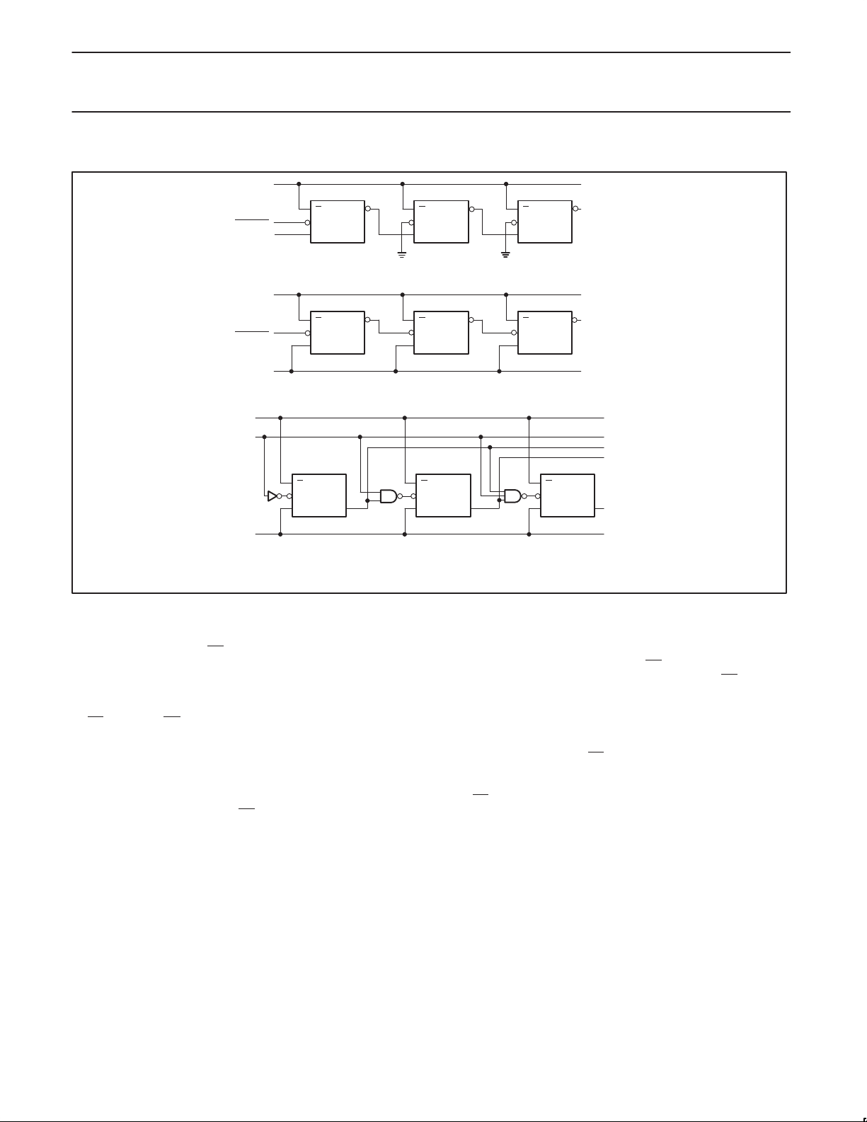
APPLICATIONS
DIRECTION CONTROL
DIRECTION CONTROL
DIRECTION CONTROL
ENABLE
CLOCK
ENABLE
CLOCK
U/D
RC RC RC
CE
CP
U/D
CE
CP
U/D
CE
CP
a. N-Stage Counter Using Ripple Clock
ENABLE
CLOCK
U/D
RC RC RC
CE
CP
U/D
CE
CP
U/D
CE
CP
b. Synchronous N-Stage Counter with Common Clock Using Ripple/Clock
U/D
CE
CP
* = Carry Gate
U/D
CE
TC TC TC
**
CP
U/D
CE
CP
c. Synchronous N-Stage Counter with Common Clock and Terminal Count
SF00733
Figure 1.
The 74F191 simplifies the design of multi-stage counters, as
indicated in Figure 1, each RC
output is used as the clock input for
the next higher stage. When the clock source has a limited drive
capability this configuration is particularly advantageous, since the
clock source drives only the first stage. It is only necessary to inhibit
the first stage to prevent counting in all stages, since a High signal
on CE
inhibits the RC output pulse as indicated in the Mode Select
Table. The timing skew between state changes in the first and last
stages is represented by the cumulative delay of the clock as it
ripples through the preceding stages. This is a disadvantage of the
configuration in some applications.
Figure 1b shows a method of causing state changes to occur
simultaneously in all stages. The RC
output signals propagate in
ripple fashion and all clock inputs are driven in parallel. The Low
state duration of the clock in this configuration must be long enough
to allow the negative-going edge of the RC
to the last stage before the clock goes High. Since the RC
signal to ripple through
output of
any package goes High shortly after its clock input goes High, there
is no such restriction on the High state duration of the clock.
In Figure 1c, the configuration shown avoids ripple delays and their
associated restrictions. The combined TC signals from all the
preceding stages forms the CE
input signal for a given stage. An
enable signal must also be included in each carry gate in order to
inhibit counting. The TC output of a given stage is not affected by its
own CE
, therefore, the simple inhibit scheme of Figure 1a and 1b
does not apply.
1995 Jul 17
5
 Loading...