

Philips N74F189AN, N74F189AD Datasheet

INTEGRATED CIRCUITS
74F189A
64-bit TTL bipolar RAM, inverting
(3-State)
Product specification
IC15 Data Handbook
1990 Feb 23
Philips Semiconductors Product specification
74F189A64-bit TTL bipolar RAM, inverting (3-State)
FEA TURES
•High speed performance
•Replaces 74F189
•Address access time: 8ns max vs 28ns for 74F189
•Power dissipation: 4.3mW/bit
•Schottky clamp TTL
•One chip enable
are fully decoded on chip. The outputs are in high impedance state
whenever the chip enable (CE) is high. The outputs are active only
in the READ mode (WE
= high) and the output data is the
complement of the stored data.
TYPICAL
SUPPL Y
CURRENT
( TOTAL)
TYPE
TYPICAL
ACCESS
TIME
74F189A 5.0ns 55mA
•Inverting outputs (for non-inverting outputs see 74F219A)
•3-State outputs
•74F189A in 150 mil wide SO is preferred options for new designs
DESCRIPTION
The 74F189A is a high speed, 64-bit RAM organized as a 16-word
by 4-bit array. Address inputs are buffered to minimize loading and
ORDERING INFORMATION
ORDER CODE
DESCRIPTION COMMERCIAL RANGE DRAWING NUMBER
VCC = 5V ±10%, T
16-pin plastic Dual In-line Package N74F189AN SOT38-4
16-pin plastic Small Outline (150mil) N74F189AD SOT109-1
= 0°C to +70°C
amb
INPUT AND OUTPUT LOADING AND FAN OUT TABLE
PINS DESCRIPTION 74F (U.L.)
D0 – D3 Data inputs 1.0/1.0 20µA/0.6mA
A0 – A3 Address inputs 1.0/1.0 20µA/0.6mA
CE Chip enable input (active low) 1.0/2.0 20µA/1.2mA
WE Write enable input (active low) 1.0/2.0 20µA/1.2mA
Q0 – Q3 Data outputs 150/40 3mA/24mA
NOTE: One (1.0) FAST unit load is defined as: 20µA in the high state and 0.6mA in the low state.
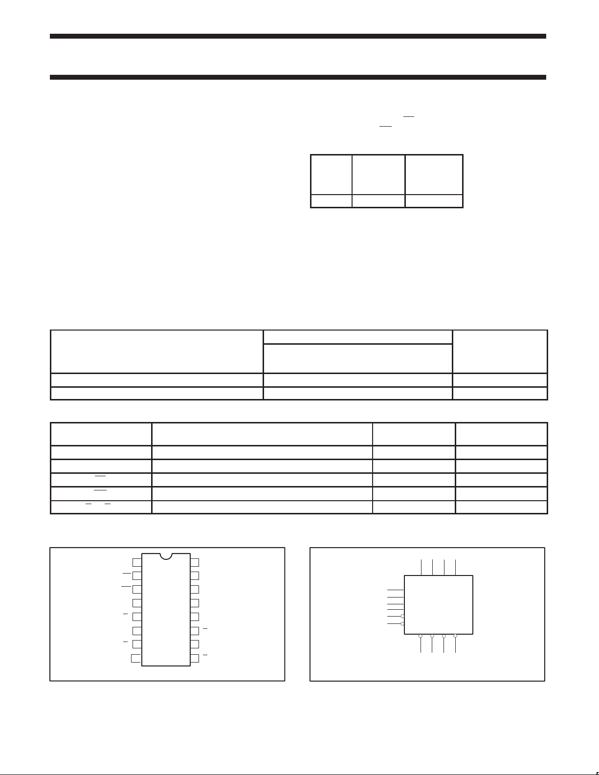
PIN CONFIGURATION
1
A0
2
CE
3
WE
4
D0
Q0
5
D1
6
Q1
GND
16
15
14
13
12
11
107
98
SF00299
V
CC
A1
A2
A3
D3
3
Q
D2
Q2
LOGIC SYMBOL
15
14
13
VCC = pin 16
GND = pin 8
1
2
3
HIGH/LOW
4
D0 D2 D3D1
A0
A1
A2
A3
CE
WE
Q0 Q1 Q2 Q3
57911
LOAD VALUE
HIGH/LOW
61012
SF00300
1990 Feb 23 853–1309 98908
2
Philips Semiconductors Product specification
74F189A64-bit TTL bipolar RAM, inverting (3-State)
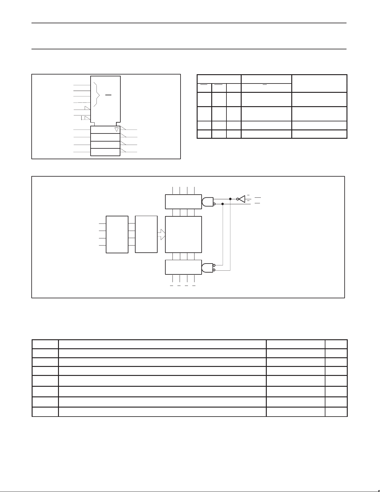
IEC/IEEE SYMBOL
1
15
14
13
2
3
4
6
10
12
LOGIC DIAGRAM
RAM 16X4
0
0
A
15
1
G1
1 EN [READ]
1 C2 [WRITE]
A,2D A
1
A0
15
A1
14
A2
13
A3
Decoder
Drivers
5
7
9
11
Address
Decoder
SF00301
D0 D1 D2 D3
4 6 10 12
Data buffers
16–word x
memory cell
FUNCTION TABLE
INPUTS OUTPUT OPERATING
CE WE Dn Q
L H X
L L L
H L H High impedance Write “1”
H X X High impedance Disable input
NOTES:
H = High voltage level
L = Low voltage level
X = Don’t care
4–bit
array
n
Complement of stored
data
High
impedance
3
WE
2
CE
MODE
Read
Write “0”
Output buffers
V
= Pin 16
CC
GND = Pin 8
57911
Q0Q1Q2Q3
SF00302
ABSOLUTE MAXIMUM RATINGS
(Operation beyond the limit set forth in this table may impair the useful life of the device. Unless otherwise noted these limits are over the
operating free air temperature range.)
SYMBOL
V
CC
V
IN
I
IN
V
OUT
I
OUT
T
amb
T
stg
Supply voltage –0.5 to +7.0 V
Input voltage –0.5 to +7.0 V
Input current –30 to +5 mA
Voltage applied to output in high output state –0.5 to V
Current applied to output in low output state 48 mA
Operating free air temperature range 0 to +70
Storage temperature range –65 to +150
PARAMETER RATING UNIT
CC
V
°C
°C
1990 Feb 23
3
 Loading...