

Philips N74F175AN, N74F175N, N74F175D, N74F175AD Datasheet
74F175*, 74F175A
Quad D flip-flop
Product specification
IC15 Data Handbook
1996 Mar 12
INTEGRATED CIRCUITS
* Discontinued part. Please see the Discontinued Product List in Section 1, page 21.
Philips Semiconductors Product specification
74F175AQuad D flip-flop
2
1996 Mar 12 853–0047 16555
FEA TURES
•Four edge-triggered D-type flip-flops
•Buffered common clock
•Buffered asynchronous Master Reset
•True and complementary outputs
•Industrial temperature range available (–40°C to +85°C)
•PNP light loading inputs
DESCRIPTION
The 74F175A is a quad, edge-triggered D-type flip-flop with
individual D inputs and both Q and Q
outputs. The common buffered
Clock (CP) and Master Reset (MR
) inputs load and reset (clear) all
flip-flops simultaneously.
The register is fully edge-triggered. The state of each D input, one
setup time before the Low-to-High clock transition is transferred to
the corresponding flip-flop’s Q output.
All Q outputs will be forced Low independently of clock or data
inputs by a Low voltage level on the MR
input. The device is useful
for applications where both true and complementary outputs are
required, and the CP and MR
are common to all storage elements.
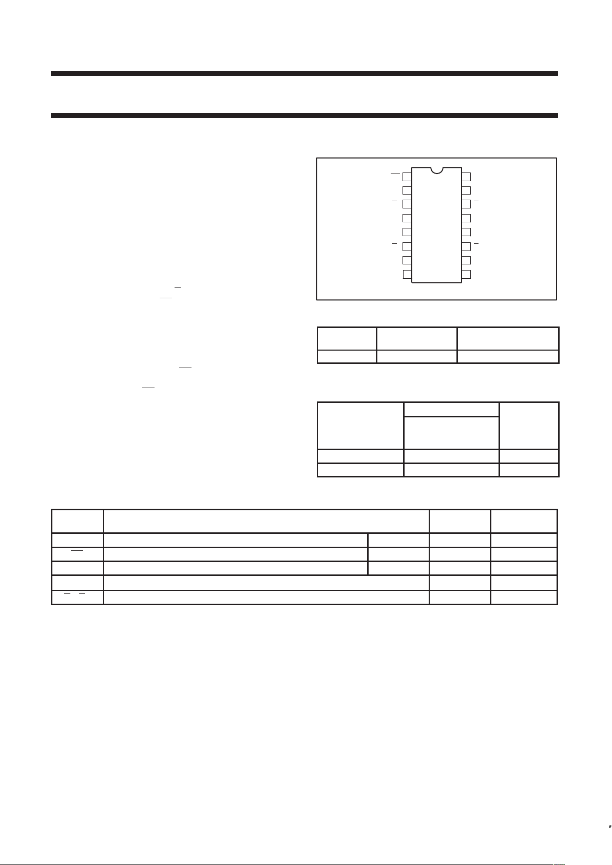
PIN CONFIGURATION
16
15
14
13
12
11
107
6
5
4
3
2
1
98
V
CC
SF00718
Q3
Q
3
D3
D2
Q
2
Q2
CP
MR
Q0
Q
0
D0
D1
Q
1
Q1
GND
TYPE TYPICAL f
max
TYPICAL SUPPL Y
CURRENT (TOTAL)
74F175A 160MHz 22mA
ORDERING INFORMATION
ORDER CODE
DESCRIPTION
COMMERCIAL RANGE
V
CC
= 5V ±10%,
T
amb
= 0°C to +70°C
PKG. DWG. #
16-pin plastic DIP 74F175AN SOT38-4
16-pin plastic SO 74F175AD SOT109-1
INPUT AND OUTPUT LOADING AND FAN OUT TABLE
PINS DESCRIPTION
74F (U.L.)
HIGH/LOW
LOAD VALUE
HIGH/LOW
D0 – D3 Data inputs 74F175A 1.0/0.033 20µA/20µA
MR Master reset input (active–Low) 74F175A 1.0/0.033 20µA/20µA
CP Clock input (active rising edge) 74F175A 1.0/0.033 20µA/20µA
Q0–Q3 True outputs 50/33 1.0mA/20mA
Q0–Q3 Complementary outputs 50/33 1.0mA/20mA
NOTE:
One (1.0) FAST unit load is defined as: 20µA in the High state and 0.6mA in the Low state.
Philips Semiconductors Product specification
74F175AQuad D flip-flop
1996 Mar 12
3
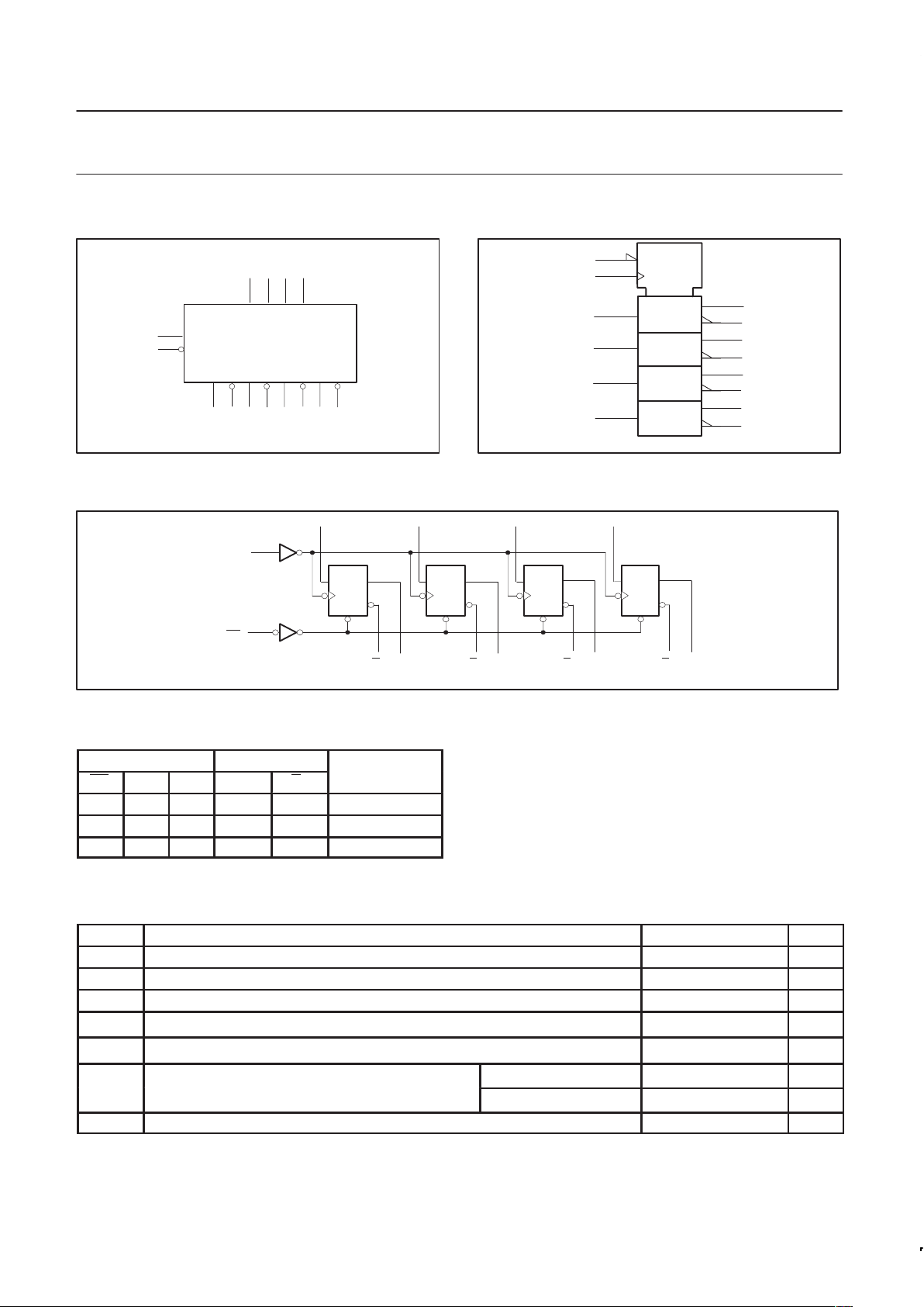
LOGIC SYMBOL
VCC = Pin 16
GND = Pin 8
SF00719
4 5 12 13
D0 D1 D2 D3
CP
MR
9
1
2 3 7 6 10 11 15 14
Q0 Q0 Q1 Q1 Q2 Q2 Q3 Q3
IEC/IEEE SYMBOL
R
C1
1D
SF00720
1
9
4
5
12
13
2
3
7
6
10
11
15
14
LOGIC DIAGRAM
DQ
RD
V
CC
= Pin 16
GND = Pin 8
CP
D0
4
DQ
RD
CP
D1
5
DQ
RD
CP
D2
12
DQ
RD
CP
D3
13
Q
SF00721
CP
MR
9
1
32 6 1110 14157
Q
0Q0 Q1Q1 Q2Q2 Q3Q3
FUNCTION TABLE
INPUTS OUTPUTS
OPERATING
MR CP Dn Q
n
Q
n
MODE
L X X L H Reset (clear)
H ↑ h H L Load “1”
H ↑ I L H Load “0”
H = High voltage level
h = High state must be present one setup time before the
Low-to-High clock transition
L = Low voltage level
l = Low state must be present one setup time before the
Low-to-High clock transition
X = Don’t care
↑ = Low-to-High clock transition
ABSOLUTE MAXIMUM RATINGS
(Operation beyond the limit set forth in this table may impair the useful life of the device.
Unless otherwise noted these limits are over the operating free air temperature range.)
SYMBOL PARAMETER RATING UNIT
V
CC
Supply voltage –0.5 to +7.0 V
V
IN
Input voltage –0.5 to +7.0 V
I
IN
Input current –30 to +5 mA
V
OUT
Voltage applied to output in High output state –0.5 to V
CC
V
I
OUT
Current applied to output in Low output state
40 mA
p
p
Commercial range 0 to +70
°C
T
amb
O erating free air tem erature range
Industrial range –40 to +85
°C
T
stg
Storage temperature range –65 to +150
°C
 Loading...