

Philips N74F173D, N74F173N Datasheet

INTEGRATED CIRCUITS
74F173
Quad D-type flip-flop (3-State)
Product specification
IC15 Data Handbook
1990 Aug 31
Philips Semiconductors Product specification
74F173Quad D-type flip–flop (3-State)
FEA TURES
• Edge–triggered D–type register
• Gated clock enable for hold ”do nothing” mode
• 3–state output buffers
• Gated output enable control
• Speed upgrade of N8T10 and current sink upgrade
• Controlled output edges to minimize ground bounces
• 48mA sinking capability
DESCRIPTION
The 74F173 is a high speed 4–bit parallel load register with
clock enable control, 3–state buffered outputs, and master
reset (MR). When the two clock enable (E
are low, the data on the D inputs is loaded into the register
simultaneously with low–to–high clock (CP) transition. When
one or both enable inputs are high one setup time before the
low–to–high clock transition, the register retains the previous
data.
TYPE TYPICAL f
74F173 125MHz 23mA
0 and E1) inputs
max
Data inputs and clock enable inputs are fully edge–triggered
and must be stable only one setup time before the
low–to–high clock transition.
The master reset (MR) is an active–high asynchronous
input. When the MR is high, all four flip–flops are reset
(cleared) independently of any other input condition.
The 3–state output buffers are controlled by a 2–input NOR
gate. When both output enable (OE
0 and OE1) inputs are
low, the data in the register is presented at the Q output.
When one or both OE
inputs are high, the outputs are forced
to a high impedance ”off” state.
The 3–state output buffers are completely independent of
the register operation; the OE
transition does not affect the
clock and reset operations.
TYPICAL SUPPLY CURRENT (TOTAL)
ORDERING INFORMATION
ORDER CODE
DESCRIPTION COMMERCIAL RANGE
= 5V ±10%, T
V
CC
16–pin plastic DIP N74F173N SOT38-4
16–pin plastic SO N74F173D SOT109-1
= 0°C to +70°C
amb
PKG DWG #
INPUT AND OUTPUT LOADING AND FAN OUT TABLE
PINS DESCRIPTION 74F (U.L.) HIGH/
LOW
D0 – D3 Data inputs 1.0/1.0 20µA/0.6mA
CP Clock input 1.0/1.0 20µA/0.6mA
E0, E1 Clock enable inputs 1.0/1.0 20µA/0.6mA
MR Master reset input 1.0/1.0 20µA/0.6mA
OE0, OE1 Output enable inputs 1.0/1.0 20µA/0.6mA
Q0 – Q3 Data outputs 750/80 15mA/48mA
Note to input and output loading and fan out table
1. One (1.0) FAST unit load is defined as: 20µA in the high state and 0.6mA in the low state.
LOAD VALUE
HIGH/LOW
August 31, 1990 853–1 160 00286
2
Philips Semiconductors Product specification
74F173Quad D-type flip–flop (3-State)
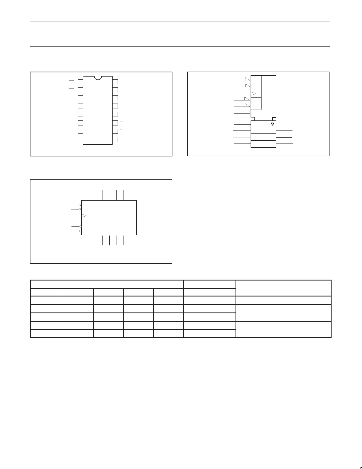
PIN CONFIGURATION
1
OE0
2
OE1
3
Q0
4
Q1
5
Q2
6
Q3
CP
GND
LOGIC SYMBOL
9
10
15
E0
E1
7
CP
MR
1
OE0
2
OE1
16
V
15
MR
14
D0
13
D3
12
D2
11
Q
107
E
98
E0
SF00290
14 13 12 11
D0 D1 D2 D3
Q0 Q1 Q2 Q3
CC
2
1
IEC/IEEE SYMBOL
14
13
12
11
&9
10
7
1
2
15
C1
&
EN
R
1D
3
4
5
6
SF00292
VCC = Pin 16
GND = Pin 8
3456
SF00291
FUNCTION TABLE
INPUTS OUTPUTS OUTPUTS
MR CP E0 E1 Dn Qn (register)
H X X X X L Reset (clear)
L ↑ l l l L Parallel load
L ↑ l l h H
L X h X X qn Hold (do nothing)
L X X h X qn
Notes to function table
H = High–voltage level
h = High state one setup time before the low–to–high clock transition
L = Low–voltage level
l = Low state one setup time before the low–to–high clock transition
qn = Lower case letters indicate the state of the referenced input (or output) on setup time prior to the low–to–high clock transition
X = Don’t care
↑ = Low–to–high clock transition
August 31, 1990
3
 Loading...