

Philips N74F166D, N74F166N Datasheet
INTEGRATED CIRCUITS
74F166
8-bit bidirectional universal shift register
Product specification
IC15 Data Handbook
1991 Feb 14

Philips Semiconductors Product specification
74F1668-bit bidirectional universal shift register
FEA TURES
• High impedance NPN base inputs for reduced loading
(20µA in high and low states)
• Synchronous parallel to serial applications
• Synchronous serial data input for easy expansion
• Clock enable for ”do nothing” mode
• Asynchronous master reset
• Expandable to 16 bits in 8–bit increments
• Industrial temperature range available (–40°C to +85°C)
For expansion of the register in parallel to serial converters,
the Q7 output is connected to the Ds input of the succeeding
stage. The clock input is gated OR structure which allows
one input to be used as an active–low clock enable (CE
input. The pin assignment for the CP and CE
inputs is
arbitrary and can be reversed for layout convenience. The
low–to–high transition of CE
input should only take place
while the CP is high for predictable operation. A low on the
master reset (MR
) input overrides all other inputs and clears
the register asynchronously , forcing all bit positions to a low
DESCRIPTION
state.
The 74F166 is a high speed 8–bit shift register that has fully
synchronous serial parallel data entry selected by an active
low parallel enable (PE
time before the low–to–high clock transition, parallel data is
entered into the register.
When PE
is high, data is entered into internal bit position Q0
) input. When the PE is low one setup
TYPE TYPICAL f
74F166 175MHz 50mA
max
TYPICAL SUPPL Y CUR-
RENT( TOTAL)
from serial data input (Ds), and the remaining bits are shifted
one place to the right (Q0 → Q1 → Q2, etc.) with each
positive going clock transition.
ORDERING INFORMATION
ORDER CODE
COMMERCIAL RANGE INDUSTRIAL RANGE
DESCRIPTION
16–pin plastic DIP N74F166N I74F166N SOT38-4
16–pin plastic SO N74F166D I74F166D SOT109-1
VCC = 5V ±10%, VCC = 5V ±10%,
T
= 0°C to +70°C T
amb
= –40°C to +85°C
amb
PKG DWG #
)
INPUT AND OUTPUT LOADING AND FAN OUT TABLE
PINS DESCRIPTION 74F (U.L.) HIGH/
D0 – D7 Parallel data inputs 1.0/0.033
Ds Serial data input (shift right) 2.0/0.066
CP Clock input (active rising edge) 1.0/0.033
CE Clock enable input (active low) 1.0/0.033
PE Parallel enable input (active low) 1.0/0.033
MR Master reset input (active low) 2.0/0.066
Q7 Data output 50/33
Note to input and output loading and fan out table
1. One (1.0) FAST unit load is defined as: 20µA in the high state and 0.6mA in the low state.
LOW
LOAD VALUE HIGH/
LOW
20µA/20µA
40µA/40µA
20µA/20µA
20µA/20µA
20µA/20µA
40µA/40µA
1.0mA/20mA
Feb. 14, 1991 853–0349 01718
2
Philips Semiconductors Product specification
74F1668-bit bidirectional universal shift register
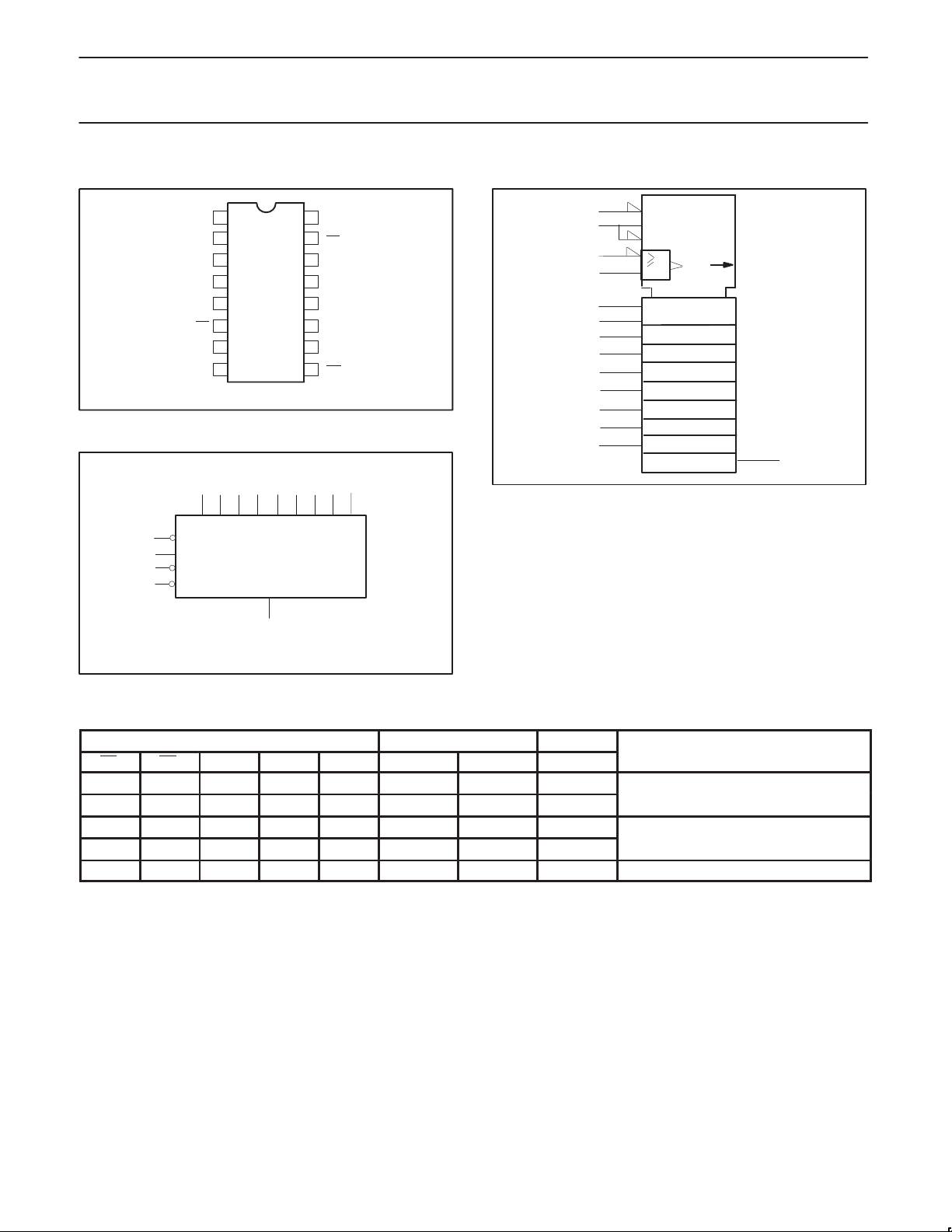
PIN CONFIGURATION
1
Ds
2
D0
3
D1
4
D2
5
D3
6
CE
CP
GND
LOGIC SYMBOL
1234510111214
6
7
9
15
V
CC
GND = Pin 8
Ds D0 D1 D2 D3 D4 D5 D6 D7
CE
CP
MR
PE
= Pin 16
Q7
IEC/IEEE SYMBOL
16
V
CC
15
PE
14
D7
13
Q7
12
D6
11
D5
107
D4
98
MR
SP000283
13
SF00284
9
15
6
7
1
2
3
4
5
10
11
12
14
SRG 8
R
M1 [SHIFT]
M2 [LOAD]
1
1, 3D
2, 3D
2,3D
C3/1
13
SF00285
FUNCTION TABLE
INPUTS Qn REGISTER OUTPUT OPERATING MODE
PE CE CP DS D0 –D7 Q0 Q1 – Q6 Q7
l l ↑ X l – l L L – L L Parallel load
l l ↑ X h – h H H – H H
h l ↑ l X – X L q0 – q5 q6 Serial shift
h l ↑ h X – X H q0 – q5 q6
X h X X X – X qn q1 – q6 q7 Hold (do nothing)
Notes to function table
1. H = High–voltage level
2. h = High voltage level one setup time before the low–to–high clock transition
3. L = Low–voltage level
4. l = Low voltage level one setup time before the low–to–high clock transition
5. qn = Lower case letters indicate the state of the referenced input (or output) one setup time prior to the low–to–high clock transition
6. X = Don’t care
7. ↑ = Low–to–high clock transition
Feb. 14, 1991
3
Philips Semiconductors Product specification
74F1668-bit bidirectional universal shift register
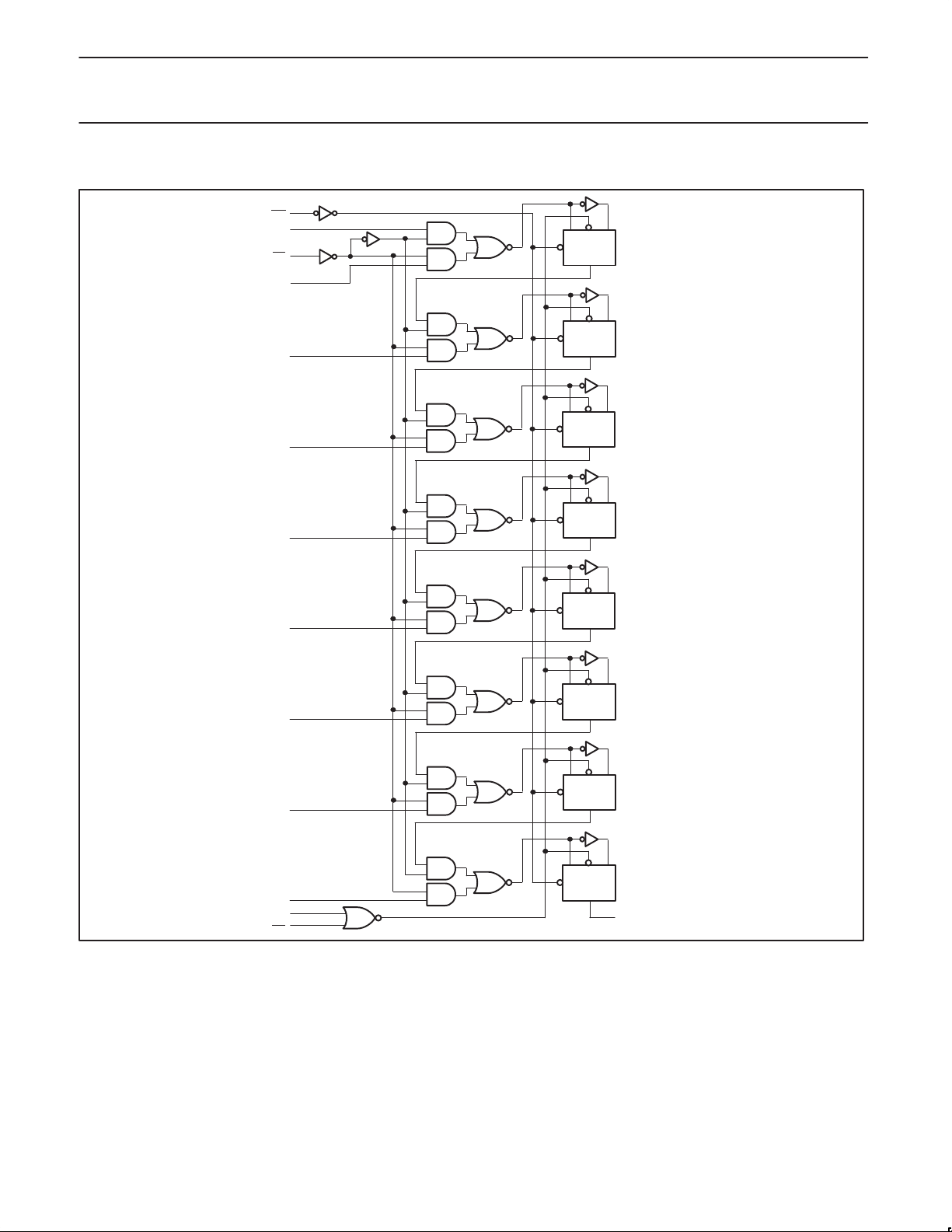
LOGIC DIAGRAM
9
MR
1
DS
D1
D2
PE
D0
15
2
3
4
RCP S
Q
RCP S
Q
RCP S
Q
V
= Pin 16
CC
GND = Pin 8
D3
D4
D5
D6
D7
CP
CE
RCP S
5
10
11
12
14
7
6
Q
RCP S
Q
RCP S
Q
RCP S
Q
RCP S
Q
13
Q7
SF00286
Feb. 14, 1991
4
 Loading...