Philips N74F132N, N74F132D Datasheet

INTEGRATED CIRCUITS
74F132
Quad 2-input NAND Schmitt trigger
Product specification
IC15 Data Handbook
1991 Jun 26

Philips Semiconductors Product specification
74F132Quad 2-input NAND Schmitt trigger
DESCRIPTION
The 74F132 contains four 2-input NAND gates which accept
standard TTL input signals and provide standard TTL output levels.
They are capable of transforming slowly changing input signals into
sharply defined, jitter-free output signals. In addition, they have
greater noise margin than conventional NAND gates. Each circuit
contains a 2-input Schmitt trigger followed by a Darlington level
shifter and a phase splitter driving a TTL totem-pole output. The
Scmitt trigger uses positive feedback to effectively speed-up slow
input transitions and provide different input threshold voltages for
positive and negative-going transitions. This hysteresis between the
positive-going and negative-going input threshold (typically 800mV)
is determined by resistor ratios and is essentially insensitive to
temperature and supply voltage variations. As long as three inputs
remain at a more positive voltage than V
respond in the transition of the other input as shown in Waveform 1.
T+MAX
, the gate will
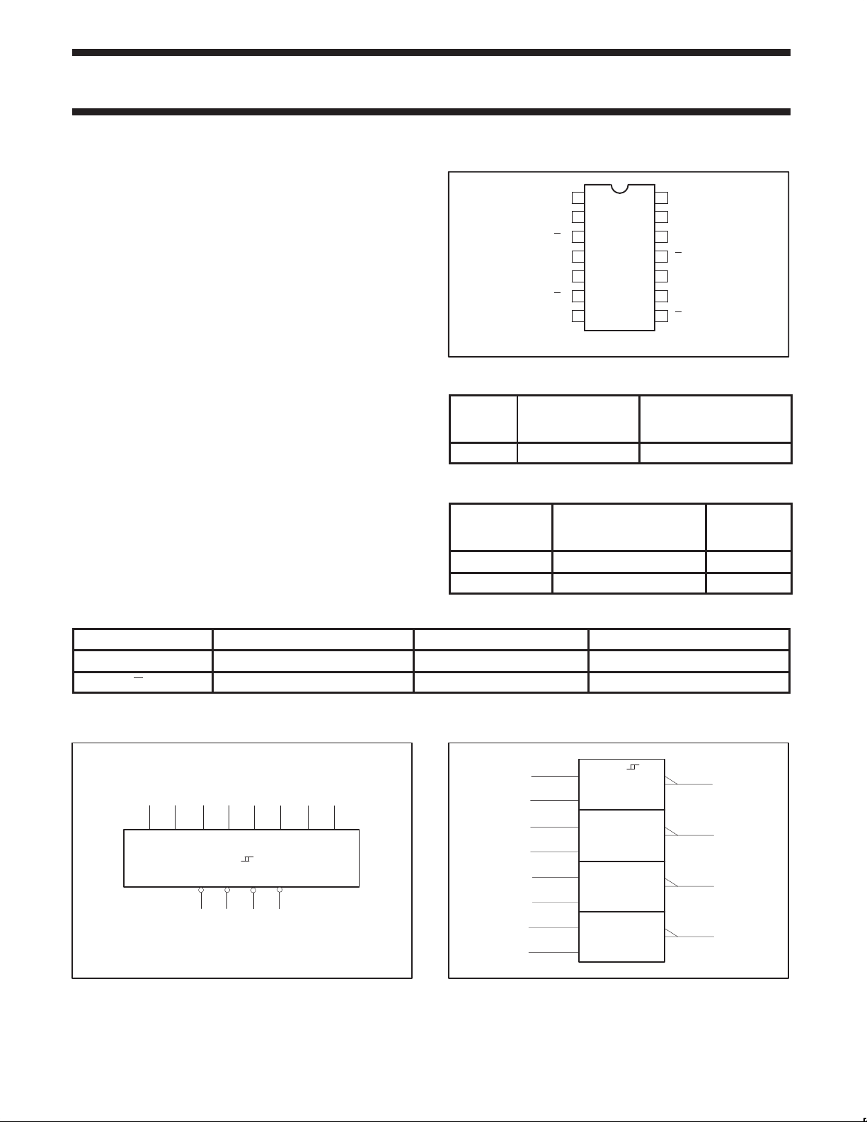
PIN CONFIGURATION
1
D0a
2
D0b
3
0
Q
4
D1a
5
D1b
6
Q
1
7
GND
TYPE TYPICAL
PROPAGATION
DELAY
74F132 6.3ns 13mA
14
V
CC
D3b
13
D3a
12
Q3
11
D2b
10
D2a
9
Q2
8
SF00710
TYPICAL
SUPPLY CURRENT
(TOTAL)
ORDERING INFORMATION
COMMERCIAL RANGE
DESCRIPTION
14-pin plastic DIP N74F132N SOT27-1
14-pin plastic SO N74F132D SOT108-1
VCC = 5V ±10%,
T
= 0°C to +70°C
amb
PKG DWG #
INPUT AND OUTPUT LOADING AND FAN-OUT TABLE
PINS DESCRIPTION 74F (U.L.) HIGH/LOW LOAD VALUE HIGH/LOW
Dna, Dnb Data inputs 1.0/1.0 20µA/0.6mA
Qn Data output 50/33 1.0mA/20mA
NOTE: One (1.0) FAST unit load is defined as: 20µA in the High state and 0.6mA in the Low state.
LOGIC SYMBOL
12459101213
D0a D0b D1a D2a D2b D3a D3bD1b
VCC = Pin 14
GND = Pin 7
Q0 Q1 Q2 Q3
36811
SF00711
IEC/IEEE SYMBOL
1
2
4
5
9
10
12
13
&
3
6
8
11
SF00712
1991 Jun 26 853–0342 03094
2

Philips Semiconductors Product specification
SYMBOL
PARAMETER
UNIT
74F132Quad 2-input NAND Schmitt trigger
LOGIC DIAGRAM
VCC = Pin 14
GND = Pin 7
D0a
D0b
D1a
D1b
D2a
D2b
D3a
D3b
1
2
4
5
9
10
12
13
3
6
8
11
SF00002
Q
0
Q1
Q
2
3
Q
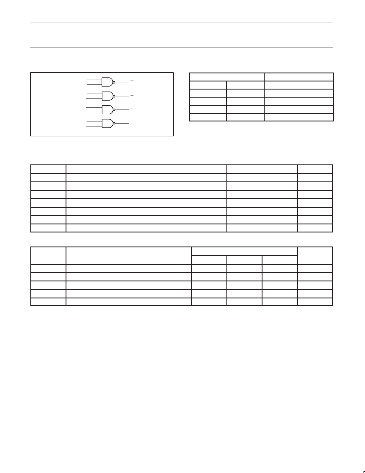
FUNCTION TABLE
Dna Dnb Qn
L L H
L H H
H L H
H H L
NOTES:
H = High voltage level
L = Low voltage level
ABSOLUTE MAXIMUM RATINGS
(Operation beyond the limits set forth in this table may impair the useful life of the device.
Unless otherwise noted these limits are over the operating free-air temperature range.)
SYMBOL
V
CC
V
IN
I
IN
V
OUT
I
OUT
T
amb
T
stg
Supply voltage –0.5 to +7.0 V
Input voltage –0.5 to +7.0 V
Input current –30 to +5 mA
Voltage applied to output in High output state –0.5 to V
Current applied to output in Low output state 40 mA
Operating free-air temperature range 0 to +70 °C
Storage temperature –65 to +150 °C
PARAMETER RATING UNIT
INPUTS OUTPUT
CC
V
RECOMMENDED OPERATING CONDITIONS
V
I
I
I
T
CC
IK
OH
OL
amb
Supply voltage 4.5 5.0 5.5 V
Input clamp current –18 mA
High-level output current –1 mA
Low-level output current 20 mA
Operating free-air temperature range 0 +70 °C
LIMITS
MIN NOM MAX
1991 Jun 26
3
 Loading...