

Philips N74F109N, N74F109D Datasheet
INTEGRATED CIRCUITS
74F109
Positive J-K
flip-flops
Product specification
IC15 Data Handbook
positive edge-triggered
1990 Oct 23
Philips Semiconductors Product specification
74F109Postive J-K positive edge-triggered flip-flops
FEA TURE
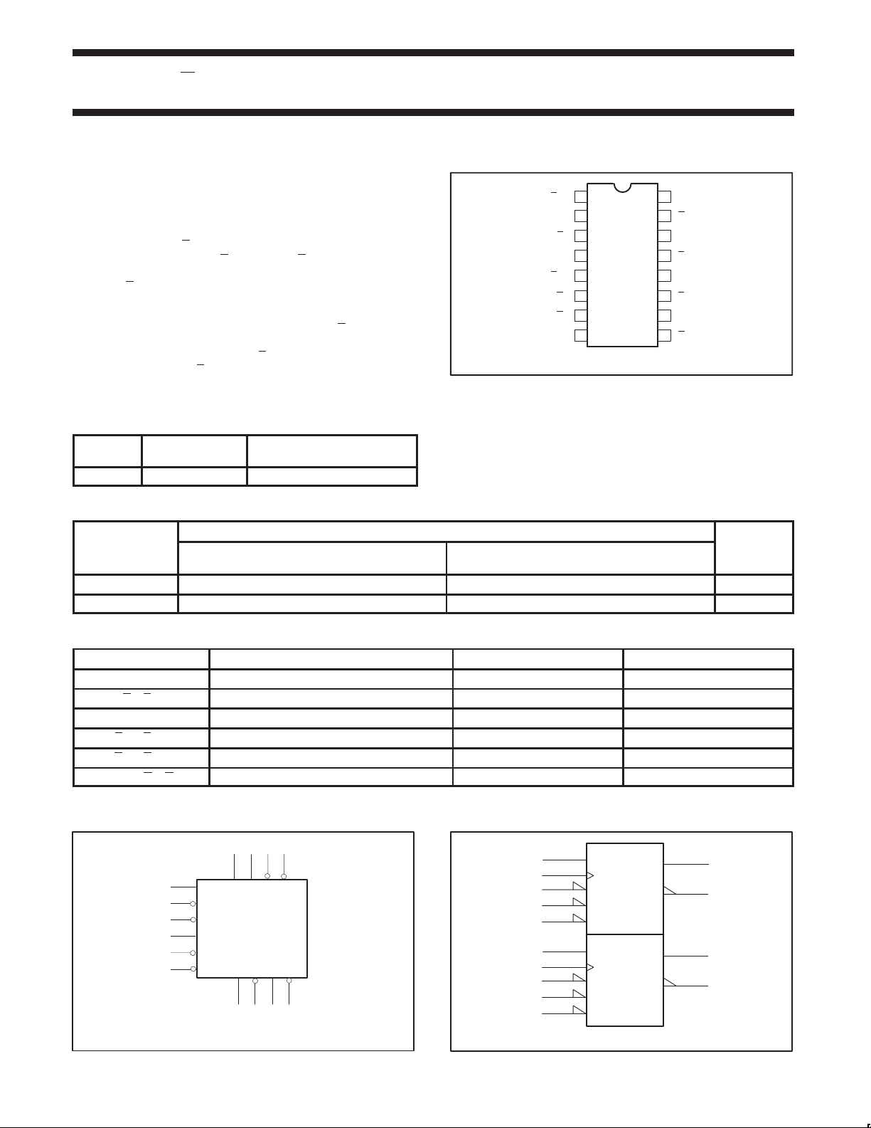
PIN CONFIGURATION
•Industrial temperature range available (–40°C to +85°C)
1
D0
R
2
CP0
S
J0
K
3
0
4
D0
5
0
6
Q
Q
0
DESCRIPTION
The 74F109 is a dual positive edge-triggered JK-type flip-flop
featuring individual J, K
complementary outputs. Set (S
active low inputs and operate independently of the clock (CP) input.
The J and K
are edge-triggered inputs which control the state
changes of the flip-flops as described in the function table. Clock
triggering occurs at a voltage level and is not directly related to the
transition time of the positive-going pulse. The J and K
, clock, set, and reset inputs; also true and
D) and reset (RD) are asynchronous
inputs must
be stable just one setup time prior to the low-to-high transition of the
clock for predictable operation. The JK
D flip-flop by tying J and K
inputs together. Although the clock input
design allows operation as a
is level sensitive, the positive transition of the clock pulse between
the 0.8V and 2.0V levels should be equal to or less than the clock to
output delay time for reliable operation.
TYPE TYPICAL f
TYPICAL SUPPL Y CURRENT
max
(TOTAL)
74F109 125MHz 12.3mA
ORDERING INFORMATION
ORDER CODE
DESCRIPTION
16-pin plastic DIP N74F109N I74F109N SOT38-4
16-pin plastic SO N74F109D I74F109D SOT109-1
COMMERCIAL RANGE
VCC = 5V ±10%, T
= 0°C to +70°C
amb
VCC = 5V ±10%, T
INDUSTRIAL RANGE
= –40°C to +85°C
amb
16
15
14
13
12
11
107
98GND Q1
SF00135
V
R
J1
K1
CP1
SD1
Q1
CC
D1
PKG DWG #
INPUT AND OUTPUT LOADING AND FAN OUT TABLE
PINS DESCRIPTION 74F (U.L.) HIGH/LOW LOAD V ALUE HIGH/LOW
J0, J1 J inputs 1.0/1.0 20µA/0.6mA
K0, K1 K inputs 1.0/1.0 20µA/0.6mA
CP0, CP1 Clock inputs (active rising edge) 1.0/1.0 20µA/0.6mA
SD0, SD1 Set inputs (active Low) 1.0/3.0 20µA/1.8mA
RD0, RD1 Reset inputs (active Low) 1.0/3.0 20µA/1.8mA
Q0, Q1, Q0, Q1 Data outputs 50/33 1.0mA/20mA
NOTE: One (1.0) FAST unit load is defined as: 20µA in the High state and 0.6mA in the Low state.
LOGIC SYMBOL
4
5
1
12
11
15
VCC = Pin 16
GND = Pin 8
CP0
SD0
RD0
CP1
SD1
RD1
2 14 3 13
J1
K0
J0
Q0 Q0 Q1 Q1
6 7 10 9
SF00136
K1
IEC/IEEE SYMBOL
2
4
3
1
5
14
12
13
15
11
1J
C1
1K
R
S
2J
C2
2K
R
S
SF00137
6
7
10
9
October 23, 1990 853–0337 00783
2
Philips Semiconductors Product specification
OPERATING MODE
T
Operating free-air temperature range
SYMBOL
PARAMETER
UNIT
T
Operating free-air temperature range
74F109Postive J-K positive edge-triggered flip-flops
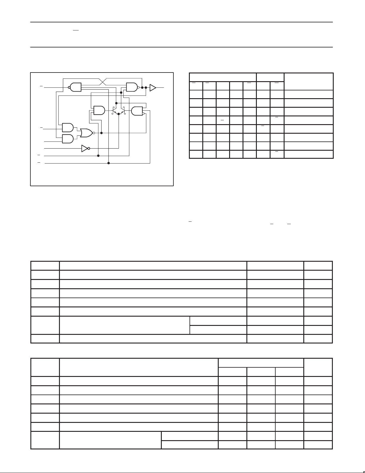
LOGIC DIAGRAM
7, 9
Q
3, 13
K
2, 14
J
4, 12
CP
5, 11
S
D
1, 15
R
D
V
= Pin 16
CC
GND = Pin 8
6, 10
SF00138
FUNCTION TABLE
INPUTS OUTPUTS
Q
SD RD CP J K Q Q
L H X X X H L Asynchronous set
H L X X X L H Asynchronous reset
L L X X X H H Undetermined*
H H ↑ X X q q Hold
H H ↑ h l q q Toggle
H H ↑ h h H L Load ”1” (set)
H H ↑ l l L H Load ”0” (reset)
H H ↑ l h q q Hold ’no change”
NOTES:
H = High-voltage level
h = High-voltage level one setup time prior to low-to-high
clock transition
L = Low-voltage level
l = Low-voltage level one setup time prior to low-to-high
clock transition
q = Lower case indicate the state of the referenced output
prior to the low-to-high clock transition
X = Don’t care
↑ = Low-to-high clock transition
= Not low-to-high clock transition
↑
* = Both outputs will be high if both S
D and RD go low
simultaneously
ABSOLUTE MAXIMUM RATINGS
(Operation beyond the limit set forth in this table may impair the useful life of the device. Unless otherwise noted these limits are over the
operating free air temperature range.)
SYMBOL
V
CC
V
IN
I
IN
V
OUT
I
OUT
amb
T
stg
Supply voltage –0.5 to +7.0 V
Input voltage –0.5 to +7.0 V
Input current –30 to +5 mA
Voltage applied to output in High output state –0.5 to V
Current applied to output in Low output state 40 mA
p
p
Storage temperature range –65 to +150 °C
PARAMETER RATING UNIT
CC
Commercial range 0 to +70 °C
Industrial range –40 to +85 °C
RECOMMENDED OPERATING CONDITIONS
LIMITS
MIN NOM MAX
V
V
V
I
I
I
CC
IN
IL
IK
OH
OL
amb
Supply voltage 4.5 5.0 5.5 V
High-level input voltage 2.0 V
Low-level input voltage 0.8 V
Input clamp current –18 mA
High-level output current –1 mA
Low-level output current 20 mA
p
p
Commercial range 0 +70 °C
Industrial range –40 +85 °C
V
October 23, 1990
3
 Loading...