

Philips MMBTA92 Datasheet
DISCRETE SEMICONDUCTORS
DATA SH EET
, halfpage
M3D088
MMBTA92
PNP high-voltage transistor
Product specification 2000 Apr 11
Philips Semiconductors Product specification
PNP high-voltage transistor MMBTA92
FEATURES
• Low current (max. 100 mA)
• High voltage (max. 300 V).
APPLICATIONS
• Telephony
• Professional communication equipment.
DESCRIPTION
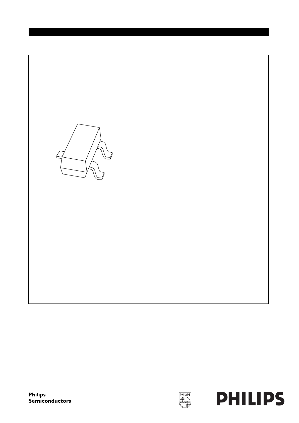
PNP high-voltage transistor in a SOT23 plastic package.
NPN complement: MMBTA42.
MARKING
TYPE NUMBER MARKING CODE
(1)
MMBTA92 7E∗
Note
1. ∗ = p: made in Hong Kong.
∗ = t: made in Malaysia.
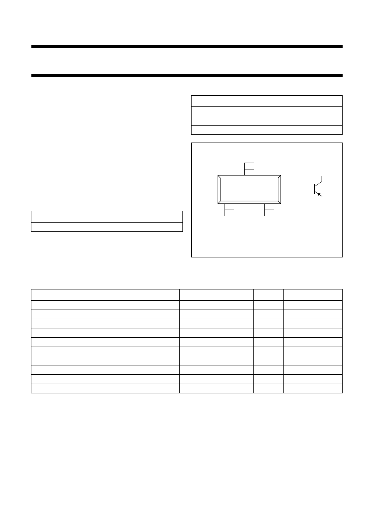
PINNING
PIN DESCRIPTION
1 base
2 emitter
3 collector
handbook, halfpage
Top view
3
21
MAM256
Fig.1 Simplified outline (SOT23) and symbol.
3
1
2
LIMITING VALUES
In accordance with the Absolute Maximum Rating System (IEC 60134).
SYMBOL PARAMETER CONDITIONS MIN. MAX. UNIT
V
CBO
V
CEO
V
EBO
I
C
I
CM
I
BM
P
tot
T
stg
T
j
T
amb
collector-base voltage open emitter −−300 V
collector-emitter voltage open base −−300 V
emitter-base voltage open collector −−5V
collector current (DC) −−100 mA
peak collector current −−200 mA
peak base current −−100 mA
total power dissipation T
≤ 25 °C; note 1 − 250 mW
amb
storage temperature −65 +150 °C
junction temperature − 150 °C
operating ambient temperature −65 +150 °C
Note
1. Transistor mounted on an FR4 printed-circuit board.
2000 Apr 11 2
Philips Semiconductors Product specification
PNP high-voltage transistor MMBTA92
THERMAL CHARACTERISTICS
SYMBOL PARAMETER CONDITIONS VALUE UNIT
R
th j-a
Note
1. Transistor mounted on an FR4 printed-circuit board.
CHARACTERISTICS
T
=25°C unless otherwise specified.
amb
SYMBOL PARAMETER CONDITIONS MIN. MAX. UNIT
I
CBO
I
EBO
h
FE
V
CEsat
V
BEsat
C
c
f
T
thermal resistance from junction to ambient note 1 500 K/W
collector cut-off current IE= 0; VCB= −200 V −−250 nA
emitter cut-off current IC= 0; VEB= −3V −−100 nA
DC current gain VCE= −10 V; note 1
I
= −1mA 25 −
C
I
=−10 mA 40 −
C
I
= −30 mA 25 −
C
collector-emitter saturation voltage IC= −20 mA; IB= −2mA −−500 mV
base-emitter saturation voltage IC= −20 mA; IB= −2mA −−900 mV
collector capacitance IE=ie= 0; VCB= −20 V;
− 6pF
f = 1 MHz
transition frequency IC= −10 mA;VCE= −20 V;
50 − MHz
f = 100 MHz
Note
1. Pulse test: t
≤ 300 µs; δ≤0.02.
p
2000 Apr 11 3
 Loading...