

Page 1

K9K2G08U0A
K9K2G08R0A
K9K2G08X0A
FLASH MEMORY
INFORMATION IN THIS DOCUMENT IS PROVIDED IN RELATION TO SAMSUNG PRODUCTS,
AND IS SUBJECT TO CHANGE WITHOUT NOTICE.
NOTHING IN THIS DOCUMENT SHALL BE CONSTRUED AS GRANTING ANY LICENSE,
EXPRESS OR IMPLIED, BY ESTOPPEL OR OTHERWISE,
TO ANY INTELLECTUAL PROPERTY RIGHTS IN SAMSUNG PRODUCTS OR TECHNOLOGY. ALL
INFORMATION IN THIS DOCUMENT IS PROVIDED
ON AS "AS IS" BASIS WITHOUT GUARANTEE OR WARRANTY OF ANY KIND.
1. For updates or additional information about Samsung products, contact your nearest Samsung office.
2. Samsung products are not intended for use in life support, critical care, medical, safety equipment, or similar
applications where Product failure could result in loss of life or personal or physical harm, or any military or
defense application, or any governmental procurement to which special terms or provisions may apply.
* Samsung Electronics reserves the right to change products or specification without notice.
1
Page 2

K9K2G08U0A
K9K2G08R0A
Document Title
256M x 8 Bit NAND Flash Memory
Revision History
FLASH MEMORY
Revision No
0.0
0.1
0.2
0.3
0.4
1.0
History
1. Initial issue
1. Technical note is changed
2. Notes of AC timing characteristics are added
3. The description of Copy-back program is changed
4. TSOP package is deleted
access time : 23ns->35ns (p.9)
1. CE
1. The value of tREA is changed. (18ns->20ns)
2. EDO mode is added.
1. The flow chart to creat the initial invalid block table is changed.
1. 1.8V FBGA spec is merged
2. 3.3V FBGA package is added
3. FBGA package size is changed to 9.5 x 12
4. Leaded part is deleted
Draft Date
May. 31. 2004
Oct. 25. 2004
Feb. 14. 2005
May 4 2005
May 6 2005
Feb. 1 2006
Remark
Advance
Preliminary
The attached data sheets are prepared and approved by SAMSUNG Electronics. SAMSUNG Electronics CO., LTD. reserve the right
to change the specifications. SAMSUNG Electronics will evaluate and reply to your requests and questions about device. If you have
any questions, please contact the SAMSUNG branch office near your office.
2
Page 3

K9K2G08U0A
K9K2G08R0A
FLASH MEMORY
256M x 8 Bit NAND Flash Memory
PRODUCT LIST
Part Number Vcc Range Organization PKG Type
K9K2G08U0A-F 2.7 ~ 3.6V X8 WSOP1
K9K2G08X0A-J 1.65 ~ 1.95V X8 FBGA
FEATURES
• Voltage Supply
- 2.7 V ~3.6 V
- 1.65V ~ 1.95V
• Organization
- Memory Cell Array
- (256M + 8,192K)bit x 8bit
- Data Register
- (2K + 64)bit x8bit
• Automatic Program and Erase
- Page Program
- (2K + 64)Byte
- Block Erase
- (128K + 4K)Byte
• Page Read Operation
- Page Size
- 2K-Byte
- Random Read : 25µs(Max.)
- Serial Access : 50ns(Min.)
• Fast Write Cycle Time
- Program time : 300µs(Typ.)
- Block Erase Time : 2ms(Typ.)
• Command/Address/Data Multiplexed I/O Port
• Hardware Data Protection
- Program/Erase Lockout During Power Transitions
• Reliable CMOS Floating-Gate Technology
- Endurance : 100K Program/Erase Cycles
- Data Retention : 10 Years
• Command Register Operation
• Unique ID for Copyright Protection
• Package :
- K9K2G08U0A-FIB0
48 - Pin WSOP I (12x17x0.7mm)- Pb-free Package
- K9K2G08X0A-JCB0/JIB0
63- Ball FBGA (9.5x12) - Pb-free Package
GENERAL DESCRIPTION
Offered in 256Mx8bit the K9K2G08X0A is 2G bit with spare 64M bit capacity. Its NAND cell provides the most cost-effective solution
for the solid state mass storage market. A program operation can be performed in typical 300µs on the 2112byte page and an erase
operation can be performed in typical 2ms on a 128K-byte block. Data in the data page can be read out at 50ns cycle time per byte.
The I/O pins serve as the ports for address and data input/output as well as command input. The on-chip write controller automates all
program and erase functions including pulse repetition, where required, and internal verification and margining of data. Even the
write-intensive systems can take advantage of the K9K2G08X0A′s extended reliability of 100K program/erase cycles by providing
ECC(Error Correcting Code) with real time mapping-out algorithm. The K9K2G08X0A is an optimum solution for large nonvolatile
storage applications such as solid state file storage and other portable applications requiring non-volatility.
3
Page 4

K9K2G08U0A
K9K2G08R0A
PIN CONFIGURATION (WSOP1)
K9K2G08U0A-FIB0
N.C
1
N.C
N.C
N.C
N.C
R/B
RE
CE
N.C
Vcc
Vss
N.C
CLE
ALE
WE
WP
N.C
N.C
N.C
N.C
2
3
4
5
6
7
8
9
10
11
12
13
14
15
16
17
18
19
20
21
22
23
24
DNU
DNU
DNU
DNU
PACKAGE DIMENSIONS
48-PIN LEAD PLASTIC VERY VERY THIN SMALL OUT-LINE PACKAGE TYPE (I)
48
47
46
45
44
43
42
41
40
39
38
37
36
35
34
33
32
31
30
29
28
27
26
25
FLASH MEMORY
N.C
N.C
DNU
N.C
I/O7
I/O6
I/O5
I/O4
N.C
DNU
N.C
Vcc
Vss
N.C
DNU
N.C
I/O3
I/O2
I/O1
I/O0
N.C
DNU
N.C
N.C
48 - WSOP1 - 1217F
#1
+0.07
-0.03
0.16
+0.07
-0.03
0.20
0.50TYP
(0.50±0.06)
#24
15.40±0.10
#48
#25
0.70 MAX
0.58±0.04
(0.01Min)
Unit :mm
12.00±0.10
12.40MAX
17.00±0.20
+0.075
-0.035
0.10
0
°
~
8
°
0.45~0.75
4
Page 5

K9K2G08U0A
PIN CONFIGURATION (FBGA)
K9K2G08R0A
K9F1G08X0A-JCB0/JIB0
3456 1 2
FLASH MEMORY
N.C N.C
N.C
A
B
C
D
E
F
G
H
N.C N.C
N.C
/RE CLE
NC
NC
NC
NC NC
NC NC NC
NC NC
NC
NC
NCNCNC
NC NC
NCNC I/O0
I/O1NC NC Vcc I/O5 I/O7
N.C N.C
N.C
N.C
R/B/WE/CEVssALE/WP
NC
NC
NC
NC
NCNC
NC
Vcc
VssI/O6I/O4I/O3I/O2Vss
N.C N.C
N.C
N.CN.C
Top View
5
Page 6

K9K2G08U0A
PACKAGE DEMENSIONS(FBGA)
K9K2G08R0A
FLASH MEMORY
#A1
Top V iew
9.50±0.10
Bottom View
#A1 INDEX MARK(OPTIONAL)
9.50±0.10
0.80 x 9= 7.20
0.80 x 5= 4.00
0.80
65
(Datum A)
A
B
(Datum B)
12.00±0.10
2.80
C
D
E
F
G
H
4321
A
B
0.80
12.00±0.10
0.80 x 7= 5.60
0.80 x 11= 8.80
0.10MAX
63-∅0.45±0.05
∅
0.20
M
A B
Side View
12.00±0.10
2.00
0.45±0.05
1.20(Max)
0.25(Min.)
6
Page 7

K9K2G08U0A
K9K2G08R0A
PIN DESCRIPTION
Pin Name Pin Function
DATA INPUTS/OUTPUTS
I/O0 ~ I/O7
CLE
The I/O pins are used to input command, address and data, and to output data during read operations. The
I/O pins float to high-z when the chip is deselected or when the outputs are disabled.
COMMAND LATCH ENABLE
The CLE input controls the activating path for commands sent to the command register. When active high,
commands are latched into the command register through the I/O ports on the rising edge of the WE
FLASH MEMORY
signal.
ALE
CE
RE
WE
WP
R/B
Vcc
Vss GROUND
ADDRESS LATCH ENABLE
The ALE input controls the activating path for address to the internal address registers. Addresses are
latched on the rising edge of WE
CHIP ENABLE
The CE
the device does not return to standby mode in program or erase opertion. Regarding CE
operation, refer to ’Page read’ section of Device operation .
READ ENABLE
The RE
tREA after the falling edge of RE
WRITE ENABLE
The WE
the WE
WRITE PROTECT
The WP
generator is reset when the WP
READY/BUSY OUTPUT
The R/B
random read operation is in process and returns to high state upon completion. It is an open drain output
and does not float to high-z condition when the chip is deselected or when outputs are disabled.
POWER
VCC is the power supply for device.
with ALE high.
input is the device selection control. When the device is in the Busy state, CE high is ignored, and
control during read
input is the serial data-out control, and when active drives the data onto the I/O bus. Data is valid
which also increments the internal column address counter by one.
input controls writes to the I/O port. Commands, address and data are latched on the rising edge of
pulse.
pin provides inadvertent write/erase protection during power transitions. The internal high voltage
pin is active low.
output indicates the status of the device operation. When low, it indicates that a program, erase or
N.C
NOTE:
1. Connect all VCC and VSS pins of each device to common power supply outputs.
2. Do not leave VCC or VSS disconnected.
NO CONNECTION
Lead is not internally connected.
7
Page 8
K9K2G08U0A
K9K2G08R0A
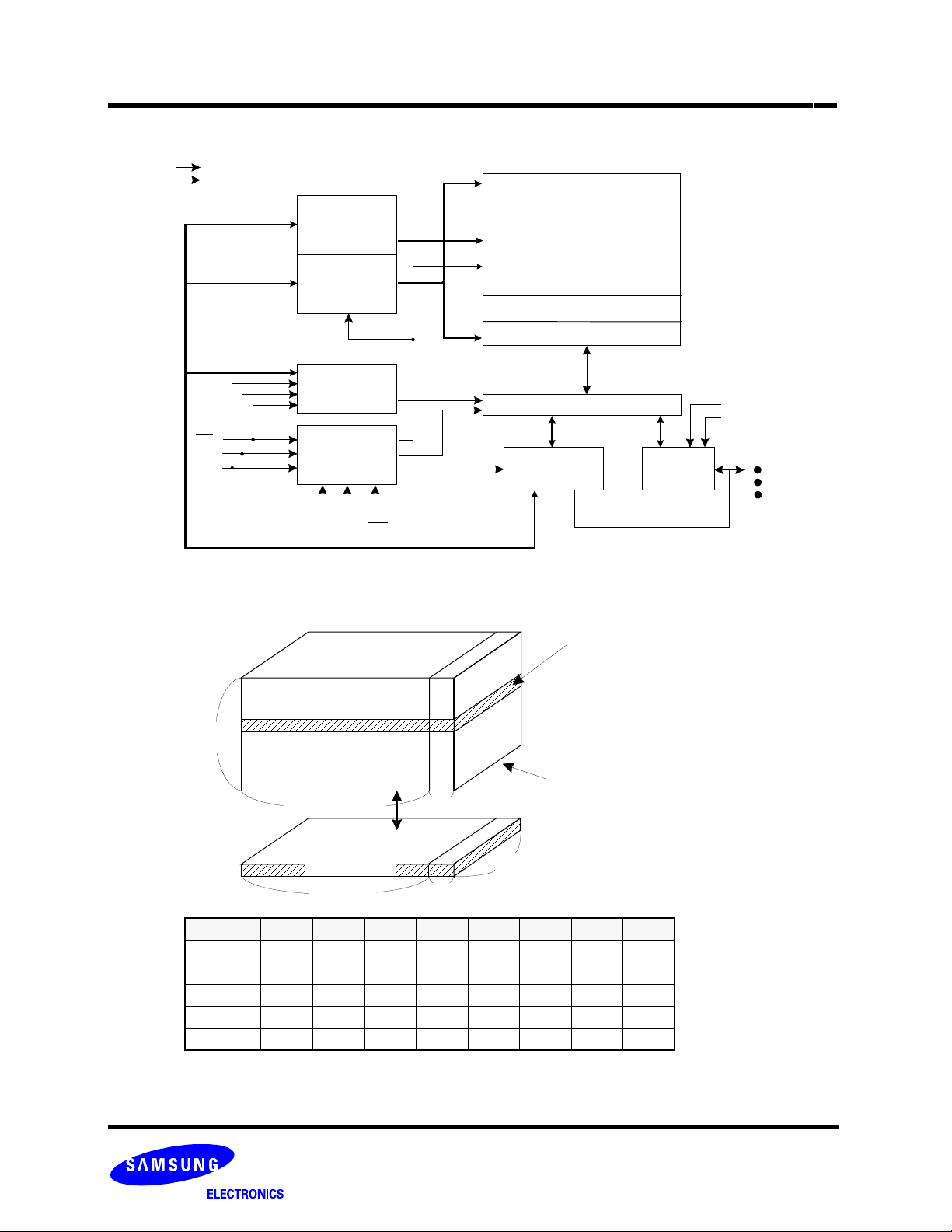
Figure 1. Functional Block Diagram
VCC
SS
V
FLASH MEMORY
A12 - A28
A0 - A11
Command
CE
RE
WE
X-Buffers
Latches
& Decoders
Y-B uff ers
Latches
& Decoders
Command
Control Logic
& High Voltage
Generator
CLE
Figure 2 Array Organization
Register
ALE
WP
2048M + 64M Bit
NAND Flash
ARRAY
(2048 + 64)Byte x 131072
Data Register & S/A
Y-G ati ng
I/O Buffers & Latches
Global Buffers
1 Block = 64 Pages
(128K + 4k) Byte
Output
Driver
VCC
VSS
I/0 0
I/0 7
128K Pages
(=2,048 Blocks)
2K Bytes 64 Bytes
Page Register
2K Bytes
I/O 0 I/O 1 I/O 2 I/O 3 I/O 4 I/O 5 I/O 6 I/O 7
1st Cycle A
2nd Cycle A8 A9 A10 A11 *L *L *L *L
3rd Cycle A
4th Cycle A20 A21 A22 A23 A24 A25 A26 A27
5th Cycle A28 *L *L *L *L *L *L *L
NOTE : Column Address : Starting Address of the Register.
* L must be set to "Low".
* The device ignores any additional input of address cycles than required.
0 A1 A2 A3 A4 A5 A6 A7
12 A13 A14 A15 A16 A17 A18 A19
1 Page = (2K + 64)Bytes
1 Block = (2K + 64)B x 64 Pages
= (128K + 4K) Bytes
1 Device = (2K+64)B x 64Pages x 2048 Blocks
= 2112 Mbits
8 bit
I/O 0 ~ I/O 7
64 Bytes
Column Address
Column Address
Row Address
Row Address
Row Address
8
Page 9

K9K2G08U0A
K9K2G08R0A
Product Introduction
The K9K2G08X0A is a 2112Mbit(2,214,592,512 bit) memory organized as 131,072 rows(pages) by 2112x8 columns. Spare 64 columns are located from column address of 2048~2111. A 2112-byte data register is connected to memory cell arrays for accommodating data transfer between the I/O buffers and memory cells during page read and page program operations. The memory array is
made up of 32 cells that are serially connected to form a NAND structure. Each of the 32 cells resides in a different page. A block
consists of two NAND structures. A NAND structure consists of 32 cells. Total 135,168 NAND cells reside in a block. The program and
read operations are executed on a page basis, while the erase operation is executed on a block basis. The memory array consists of
2048 separately erasable 128K-byte blocks. It indicates that the bit by bit erase operation is prohibited on the K9K2G08X0A.
The K9K2G08X0A has addresses multiplexed into 8 I/Os. This scheme dramatically reduces pin counts and allows system upgrades
to future densities by maintaining consistency in system board design. Command, address and data are all written through I/O's by
bringing WE
Enable(ALE) are used to multiplex command and address respectively, via the I/O pins. Some commands require one bus cycle. For
example, Reset Command, Status Read Command and etc require just one cycle bus. Some other commands, like Page Read, Block
Erase and Page Program, require two cycles: one cycle for setup and the other cycle for execution. The 264M byte physical space
requires 29 addresses, thereby requiring five cycles for addressing: 2 cycles of column address, 3 cycles of row address, in that order.
Page Read and Page Program need the same five address cycles following the required command input. In Block Erase operation,
however, only the three row address cycles are used. Device operations are selected by writing specific commands into the command
register. Table 1 defines the specific commands of the K9K2G08X0A.
to low while CE is low. Those are latched on the rising edge of WE. Command Latch Enable(CLE) and Address Latch
FLASH MEMORY
Table 1. Command Sets
Function 1st. Cycle 2nd. Cycle Acceptable Command during Busy
Read 00h 30h
Read for Copy Back 00h 35h
Read ID 90h -
Reset FFh - O
Page Program 80h 10h
Cache Program 80h 15h
Copy-Back Program 85h 10h
Block Erase 60h D0h
Random Data Input
Random Data Output
Read Status 70h O
NOTE : 1. Random Data Input/Output can be executed in a page.
2. Cache program and Copy-Back program are supported only with 3.3V device.
Caution : Any undefined command inputs are prohibited except for above command set of Table 1.
*1
*1
85h -
05h E0h
9
Page 10

K9K2G08U0A
K9K2G08R0A
ABSOLUTE MAXIMUM RATINGS
Parameter Symbol
Voltage on any pin relative to V
Temperature Under
Bias
Storage Temperature
K9K2G08X0A-XCB0
K9K2G08X0A-XIB0 -40 to +125
K9K2G08X0A-XCB0
K9K2G08X0A-XJIB0
SS
VIN/OUT -0.6 to + 2.45 -0.6 to + 4.6
V
CC -0.6 to + 2.45 -0.6 to + 4.6
T
BIAS
T
STG -65 to +150 °C
Short Circuit Current Ios 5 mA
NOTE :
1. Minimum DC voltage is -0.6V on input/output pins. During transitions, this level may undershoot to -2.0V for periods <30ns.
Maximum DC voltage on input/output pins is V
2. Permanent device damage may occur if ABSOLUTE MAXIMUM RATINGS are exceeded. Functional operation should be restricted to the conditions
as detailed in the operational sections of this data sheet. Exposure to absolute maximum rating conditions for extended periods may affect reliability.
CC,+0.3V which, during transitions, may overshoot to VCC+2.0V for periods <20ns.
1.8V DEVICE 3.3V DEVICE
-10 to +125
RECOMMENDED OPERATING CONDITIONS
(Voltage reference to GND, :TA=0 to 70°C, K9K2G08X0A-XIB0:TA=-40 to 85°C)
Parameter Symbol
Supply Voltage V
Supply Voltage V
CC 1.65 1.8 1.95 2.7 3.3 3.6 V
SS 000000V
K9K2G08R0A(1.8V) K9K2G08U0A(3.3V)
Min Typ . Max Min Ty p. Max
FLASH MEMORY
Rating
Unit
V
°C
Unit
DC AND OPERATING CHARACTERISTICS(Recommended operating conditions otherwise noted.)
Parameter Symbol Test Conditions
Operat-
Current
Page Read with
Serial Access
ing
Program I
Erase I
Stand-by Current(TTL) I
Stand-by Current(CMOS) I
Input Leakage Current I
Output Leakage Current I
Input High Voltage V
Input Low Voltage, All
inputs
Output High Voltage
Level
Output Low Voltage Level V
Output Low Current(R/B
)IOL(R/B)
tRC=50ns, (30ns with 3.3V device)
I
CC1
CE=VIL
IOUT=0mA
CC2 - - 10 20 - 10 30
CC3 - - 10 20 - 10 30
SB1CE=VIH, WP=0V/VCC -- 1 --1
CE
SB2
LI VIN=0 to Vcc(max) - - ±20 - - ±10
LO VOUT=0 to Vcc(max) - - ±20 - - ±10
IH - 0.8xVcc - Vcc+0.3 0.8xVcc - Vcc+0.3
V
IL - -0.3 - 0.2xVcc -0.3 - 0.2xVcc
OH
V
OL
=VCC-0.2,
=0V/VCC
WP
K9K2G08R0A: IOH=-100µA
K9K2G08U0A: I
K9K2G08R0A: IOL=100mA
K9K2G08U0A: I
K9K2G08R0A: V
K9K2G08U0A: V
OH=-400µA
OL=2.1mA
OL=0.1V
OL=0.4V
K9K2G08R0A(1.8V) K9K2G08U0A(3.3V)
Min Typ Max Min Typ Max
- 10 20 - 10 30
- 20 100 - 20 100
Vcc-0.1 - - 2.4 - -
--0.1 --0.4
34 - 810-mA
Unit
mA
µA
V
10
Page 11

K9K2G08U0A
K9K2G08R0A
VALID BLOCK
Parameter Symbol Min Ty p. Max Unit
Valid Block Number N
NOTE :
1. The
K9K2G08X0A may include invalid blocks when first shipped. Additional invalid blocks may develop while being used. The number of valid
blocks is presented with both cases of invalid blocks considered. Invalid blocks are defined as blocks that contain one or more bad bits
or program factory-marked bad blocks.
2. The 1st block, which is placed on 00h block address, is fully guaranteed to be a valid block and does not require Error Correction up to 1K Program/
Earase cycles..
VB 2008 - 2048 Blocks
Refer to the attached technical notes for appropriate management of invalid blocks.
AC TEST CONDITION
(K9K2G08X0A-XCB0 :TA=0 to 70°C, K9K2G08X0A-XIB0:TA=-40 to 85°C
K9K2G08R0A : Vcc=1.65V~1.95V, K9K2G08U0A : Vcc=2.7V~3.6Vunless otherwise noted)
Parameter K9K2G08R0A K9K2G08U0A
Input Pulse Levels 0V to Vcc 0V to Vcc
Input Rise and Fall Times 5ns 5ns
Input and Output Timing Levels Vcc/2 Vcc/2
Output Load 1 TTL GATE and CL=30pF 1 TTL GATE and CL=50pF
CAPACITANCE(TA=25C, VCC=1.8V/3.3V, f=1.0MHz)
Item Symbol Test Condition Min Max Unit
Input/Output Capacitance C
Input Capacitance C
NOTE : Capacitance is periodically sampled and not 100% tested.
I/O VIL=0V - 20 pF
IN VIN=0V - 20 pF
FLASH MEMORY
. Do not erase
MODE SELECTION
CLE ALE CE WE RE WP Mode
HLL HX
Read Mode
Command Input
L H L H X Address Input(5clock)
HLL HH
Write Mode
Command Input
L H L H H Address Input(5clock)
L L L H H Data Input
LLLH X Data Output
X X X X H X During Read(Busy)
XXXXXH During Program(Busy)
XXXXXH During Erase(Busy)
X
XXHXX
NOTE : 1. X can be VIL or VIH.
2. WP should be biased to CMOS high or CMOS low for standby.
(1)
X
X X X L Write Protect
(2)
CC
Stand-by
0V/V
Program / Erase Characteristics
Parameter Symbol Min Typ Max Unit
Program Time
Dummy Busy Time for Cache Program
Number of Partial Program Cycles
in the Same Page
Main Array
Spare Array - - 4 cycles
Block Erase Time t
NOTE : 1.Typical program time is defined as the time within which more than 50% of whole pages are programmed at Vcc of 3.3V and 25°C
2. Max. time of tCBSY depends on timing between internal program completion and data in
*1
PROG
t
*2
t
CBSY
Nop
BERS -23ms
- 200 700 µs
3700
--4cycles
µs
11
Page 12

K9K2G08U0A
K9K2G08R0A
AC Timing Characteristics for Command / Address / Data Input
Parameter Symbol
CLE setup Time
CLE Hold Time t
setup Time
CE
CE
Hold Time tCH 10 5 - - ns
WE
Pulse Width tWP 25 15 - - ns
ALE setup Time
ALE Hold Time t
Data setup Time
Data Hold Time t
Write Cycle Time t
WE
High Hold Time tWH 15 10 - - ns
Address to Data Loading Time
CLS
t
CLH 10 5 - - ns
CS
t
t
ALS
ALH 10 5 - - ns
DS
t
DH 10 5 - - ns
WC 45 30 - - ns
ADL
t
K9K2G08R0A K9K2G08U0A K9K2G08R0A K9K2G08U0A
*1
*1
*1
*1
*2
25 15 - - ns
35 20 - - ns
25 15 - - ns
20 15 - - ns
100
Min Max
*2
100
*2
FLASH MEMORY
--ns
Unit
NOTE : 1. The transition of the corresponding control pins must occur only once while WE is held low.
2. tADL is the time from the WE
3. For cache program operation, the whole AC Charcateristics must be same as that of K9K2G08R0A.
rising edge of final address cycle to the WE rising edge of first data cycle.
AC Characteristics for Operation
Parameter Symbol
K9K2G08R0A K9K2G08U0A K9K2G08R0A K9K2G08U0A
Data Transfer from Cell to Register tR - - 25 25 µs
ALE to RE
CLE to RE
Ready to RE
RE Pulse Width t
WE High to Busy t
Read Cycle Time t
RE
CE
RE
CE
RE
RE
Output Hi-Z to RE
WE
Device Resetting Time (Read/Program/Erase) t
Delay tAR 10 10 - - ns
Delay tCLR 10 10 - - ns
Low tRR 20 20 - - ns
RP 25 15 - - ns
WB - - 100 100 ns
RC 50 30 - - ns
Access Time tREA - - 30 20 ns
Access Time tCEA - - 45 35 ns
High to Output Hi-Z tRHZ - - 30 30 ns
High to Output Hi-Z tCHZ - - 20 20 ns
or CE High to Output hold tOH 15 15 - - ns
High Hold Time tREH 15 10 - - ns
Low tIR 00 - -ns
High to RE Low tWHR 60 60 - - ns
RST --
Min Max
5/10/500
*1
5/10/500
*1
Unit
µs
NOTE: 1. If reset command(FFh) is written at Ready state, the device goes into Busy for maximum 5us.
2. For cache program operation, the whole AC Charcateristics must be same as that of K9K2G08R0A.
12
Page 13

K9K2G08U0A
K9K2G08R0A
NAND Flash Technical Notes
Initial Invalid Block(s)
Initial invalid blocks are defined as blocks that contain one or more initial invalid bits whose reliability is not guaranteed by Samsung.
The information regarding the initial invalid block(s) is so called as the initial invalid block information. Devices with initial invalid
block(s) have the same quality level as devices with all valid blocks and have the same AC and DC characteristics. An initial invalid
block(s) does not affect the performance of valid block(s) because it is isolated from the bit line and the common source line by a
select transistor. The system design must be able to mask out the initial invalid block(s) via address mapping. The 1st block, which is
placed on 00h block address, is fully guaranteed to be a valid block, does not require Error Correction up to 1K Program/Erase
cycles.
Identifying Initial Invalid Block(s)
All device locations are erased except locations where the initial invalid block(s) information is written prior to shipping. The initial
invalid block(s) status is defined by the 1st byte in the spare area. Samsung makes sure that either the 1st or 2nd page of every initial
invalid block has non-FFh data at the column address of 2048. Since the initial invalid block information is also erasable in most
cases, it is impossible to recover the information once it has been erased. Therefore, the system must be able to recognize the initial
invalid block(s) based on the initial invalid block information and create the initial invalid block table via the following suggested flow
chart(Figure 3). Any intentional erasure of the initial invalid block information is prohibited.
Start
FLASH MEMORY
Increment Block Address
Create (or update)
Initial Invalid Block(s) Table
Figure 3. Flow chart to create initial invalid block table.
Set Block Address = 0
No
No
Check "FFh ?
Yes
Last Block ?
Yes
End
Check "FFh" at the column address
2048 of the 1st and 2nd page in the block
*
13
Page 14

K9K2G08U0A
K9K2G08R0A
NAND Flash Technical Notes (Continued)
Error in write or read operation
Within its life time, additional invalid blocks may develop with NAND Flash memory. Refer to the qualification report for the block failure rate.The following possible failure modes should be considered to implement a highly reliable system. In the case of status read
failure after erase or program, block replacement should be done. Because program status fail during a page program does not affect
the data of the other pages in the same block, block replacement can be executed with a page-sized buffer by finding an erased
empty block and reprogramming the current target data and copying the rest of the replaced block. In case of Read, ECC must be
employed. To improve the efficiency of memory space, it is recommended that the read failure due to single bit error should be
reclaimed by ECC without any block replacement. The block failure rate in the qualification report does not include those reclaimed
blocks.
Failure Mode Detection and Countermeasure sequence
Write
Read Single Bit Failure Verify ECC -> ECC Correction
Erase Failure Status Read after Erase --> Block Replacement
Program Failure Status Read after Program --> Block Replacement
FLASH MEMORY
ECC
Program Flow Chart
: Error Correcting Code --> Hamming Code etc.
Example) 1bit correction & 2bit detection
Start
Write 80h
Write Address
Write Data
Write 10h
Read Status Register
I/O 6 = 1 ?
or R/B = 1 ?
No
*
Program Error
No
I/O 0 = 0 ?
P
rogram Completed
Yes
Yes
: If program operation results in an error, map out
*
the block including the page in error and copy the
target data to another block.
14
Page 15

K9K2G08U0A
K9K2G08R0A
NAND Flash Technical Notes (Continued)
FLASH MEMORY
Erase Flow Chart
*
Erase Error
No
Start
Write 60h
Write Block Address
Write D0h
Read Status Register
I/O 6 = 1 ?
or R/B = 1 ?
Yes
I/O 0 = 0 ?
Yes
No
Read Flow Chart
Reclaim the Error
Start
Write 00h
Write Address
Write 30h
Read Data
ECC Generation
No
Verify ECC
Yes
Page Read Completed
Erase Completed
: If erase operation results in an error, map out
*
the failing block and replace it with another block.
Block Replacement
Block A
1st
∼
{
(n-1)th
nth
(page)
1st
∼
(n-1)th
nth
(page)
* Step1
When an error happens in the nth page of the Block ’A’ during erase or program operation.
* Step2
Copy the data in the 1st ~ (n-1)th page to the same location of another free block. (Block ’B’)
* Step3
Then, copy the nth page data of the Block ’A’ in the buffer memory to the nth page of the Block ’B’.
* Step4
Do not erase or program to Block ’A’ by creating an ’invalid Block’ table or other appropriate scheme.
an error occurs.
Block B
{
1
Buffer memory of the controller.
2
15
Page 16

K9K2G08U0A
K9K2G08R0A
NAND Flash Technical Notes (Continued)
Addressing for program operation
Within a block, the pages must be programmed consecutively from the LSB (least significant bit) page of the block to MSB (most significant bit) pages of the block. Random page address programming is prohibited.
FLASH MEMORY
Page 63
Page 31
Page 2
Page 1
Page 0
From the LSB page to MSB page
DATA IN: Data (1)
(64)
:
(32)
:
(3)
(2)
(1)
Data register
Data (64)
Page 63
Page 31
Page 2
Page 1
Page 0
Ex.) Random page program (Prohibition)
DATA IN: Data (1)
(64)
:
(1)
:
(3)
(32)
(2)
Data register
Data (64)
16
Page 17

K9K2G08U0A
K9K2G08R0A
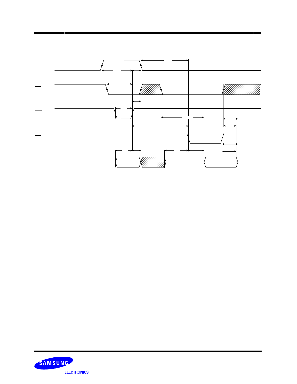
System Interface Using CE don’t-care.
For an easier system interface, CE may be inactive during the data-loading or serial access as shown below. The internal 2112byte
data registers are utilized as separate buffers for this operation and the system design gets more flexible. In addition, for voice or
audio applications which use slow cycle time on the order of µ-seconds, de-activating CE
would provide significant savings in power consumption.
Figure 4. Program Operation with CE don’t-care.
CLE
CE don’t-care
CE
FLASH MEMORY
during the data-loading and serial access
WE
ALE
I/Ox
CE
WE
80h Data Input
Address(5Cycles)
tCS
tWP
tCH
Figure 5. Read Operation with CE don’t-care.
CLE
CE
≈
CE
RE
I/O0~7
tCEA
tREA
CE
don’t-care
≈
Data Input
out
10h
RE
ALE
R/B
WE
I/Ox
≈
tR
Address(5Cycle)00h
30h
17
Data Output(serial access)
Page 18

K9K2G08U0A
K9K2G08R0A
NOTE
Device
K9K2G08X0A I/O 0 ~ I/O 7 ~2112byte A0~A7 A8~A11 A12~A19 A20~A27 A28
I/O DATA ADDRESS
I/Ox Data In/Out Col. Add1 Col. Add2 Row Add1 Row Add2 Row Add3
Command Latch Cycle
FLASH MEMORY
CLE
CE
WE
ALE
I/Ox
Address Latch Cycle
CLE
tCLS
tCLS
tCS
tALS
tWP
tDS
Command
tCLH
tCH
tALH
tDH
CE
WE
ALE
I/Ox
tCS
tALS
tWP
tDS
Col. Add1
tWC
tALH
tDH
tWH
tWP
tALS
18
tWC
tALH
tDH
tDS
Col. Add2
tWH
tWP
tALS
Row Add1
tDS
tWC
tALH
tDH
tWH
tWP
tALS
tDS
Row Add2
tALH
tDH
Page 19

K9K2G08U0A
Input Data Latch Cycle
CLE
CE
K9K2G08R0A
FLASH MEMORY
tCLH
≈
tCH
≈
ALE
WE
I/Ox
tALS
tWP
tWC
tWH
tDH
tDS
DIN 0
NOTES : DIN final means 2112
tWP
tDS
DIN 1
tDH
Serial Access Cycle after Read(CLE=L, WE=H, ALE=L)
CE
RE
tCEA
tREA
tREH
tREA
≈
≈
tWP
≈
≈
tDH
tDS
DIN final*
≈≈≈≈
tREA
tCHZ*
tOH
I/Ox
R/B
tRHZ*
Dout
tRR
NOTES : Transition is measured ±200mV from steady state voltage with load.
This parameter is sampled and not 100% tested.
tRC
Dout
19
tRHZ*
tOH
Dout
Page 20
K9K2G08U0A
Status Read Cycle
CLE
CE
WE
RE
I/Ox
K9K2G08R0A
tCLS
tCS
tWP
tDS
70h
tCLH
tCH
tDH
tWHR
tCLR
tIR*
tCEA
FLASH MEMORY
tCHZ*
tOH
tREA
Status Output
tRHZ*
tOH
20
Page 21

K9K2G08U0A
Read Operation
CLE
CE
tWC
WE
ALE
K9K2G08R0A
FLASH MEMORY
tCLR
tWB
tAR
tR
tRC
tRHZ
RE
I/Ox
00h
Col. Add1
Col. Add2
Column Address
Row Add1
R/B
Read Operation(Intercepted by CE)
CLE
CE
WE
ALE
Row Add2
Row Address
Row Add3
30h
tRR
Busy
tWB
tAR
Dout N
Dout N+1
≈
tCHZ
tOH
≈≈
Dout M
RE
I/Ox
R/B
00h
Col. Add1
Column Address
Col. Add2 Row Add1
Row Address
Row Add2
Row Add3
21
30h
tR
tRR
Busy
Dout N
tRC
Dout N+1
Dout N+2
Page 22

K9K2G08U0A
K9K2G08R0A
Dout M+1
FLASH MEMORY
tCLR
B
W
t
tWHR
tAR
tREA
C
R
t
tR
tRR
Dout M
E0h
Col Add2
Col Add1
Column Address
Dout N Dout N+1
30h 05h
Busy
Random Data Output In a Page
CLE
CE
WE
ALE
22
RE
Row Add3
Row Add2
Row Address
Row Add1
Col. Add2
Col. Add1
Column Address
00h
I/Ox
R/B
Page 23

K9K2G08U0A
Page Program Operation
CLE
CE
tWC
WE
ALE
RE
I/Ox
R/B
80h
SerialData
Input Command
Co.l Add1 Col. Add2 Row Add1 Row Add 2 Row Add3
Column Address Row Address
tWC
K9K2G08R0A
FLASH MEMORY
tWC
≈
tPROG
tADL
1 up to m Byte
≈
Din
N
≈
Serial Input
m = 2112byte
Din
M
tWB
10h
Program
Command
70h I/O
Read Status
Command
≈
I/O
0
=0 Successful Program
I/O
0
=1 Error in Program
0
NOTES : tADL is the time from the WE rising edge of final address cycle to the WE rising edge of first data cycle.
23
Page 24

K9K2G08U0A
K9K2G08R0A
0
Read Status
Command
FLASH MEMORY
≈
tPROG
tWB
10h
Program
Command
K
Din
≈
≈
tADL
≈
Din
Serial Input
J
tWC
tWC
Col. Add2
Column Address
Col. Add1
85h
Random Data
Input Command
M
Din
≈
≈≈
N
Din
Serial Input
tADL
Row Add3
rising edge of final address cycle to the WE rising edge of first data cycle.
Row Add2
Row Add1
Col. Add2
Column Address Row Address
Col. Add1
Page Program Operation with Random Data Input
CLE
CE
tWC
WE
ALE
RE
24
80h 70h I/O
I/Ox
Serial Data
Input Command
NOTES : tADL is the time from the WE
R/B
Page 25

K9K2G08U0A
K9K2G08R0A
0
Read Status
Command
tPROG
≈
Busy
=0 Successful Program
=1 Error in Program
0
0
I/O
I/O
FLASH MEMORY
tWB
10h
Data N
≈ ≈
Data 1
tADL
Row Add3
Row Add2
Row Address
Row Add1
tWC
tWB
Col Add2
Col Add1
Column Address
85h
≈
Copy-Back Data
Input Command
tR
35h
Row Add3
Row Add2
Row Address
Row Add1
Col Add2
Col Add1
Column Address
00h 70h I/O
Busy
rising edge of final address cycle to the WE rising edge of first data cycle.
NOTES : tADL is the time from the WE
Copy-Back Program Operation With Random Data Input
CLE
CE
WE
ALE
RE
I/Ox
R/B
25
Page 26

K9K2G08U0A
K9K2G08R0A
FLASH MEMORY
≈
tCPROG
tWB
I/O
70h
tPROG
70h
10h
≈
Address &
Data Input
10h
(True)
Command
Program Confirm
M
Din
80h
≈≈
N
Din
tADL
Row Add3
Row Add2
Row Add1
Col Add2
Col Add1
80h
Last Page Input & Program
tCBSY
tCBSY
15h
Address &
Data Input
80h
15h
Cache Program Operation(available only within a block)
CLE
CE
Address &
≈
tCBSY
tWB
15h
Program
Command
(Dummy)
M
Din
tADL
RE
≈≈
N
Din
Row Add3
Row Add2
Row Add1
Col Add2
Col Add1
80h
I/Ox
Serial Input
Row Address
Column Address
Serial Data
Input Command
Max. 63 times repeatable
R/B
≈
tWC
WE
ALE
CBSY :
max. 700us
t
tCBSY
Ex.) Cache Program
NOTES : tADL is the time from the WE rising edge of final address cycle to the WE rising edge of first data cycle.
R/B
Data Input
80h
15h
Address &
Data Input
Col Add1,2 & Row Add1,2
80h
I/Ox
Data
26
Page 27

K9K2G08U0A
Block Erase Operation
CLE
CE
tWC
WE
ALE
RE
K9K2G08R0A
tWB
tBERS
FLASH MEMORY
I/Ox
R/B
Row Add1
60h
Auto Block Erase
Setup Command
Row Add2 Row Add3
Row Address
D0h 70h I/O 0
Busy
Erase Command
≈
Read Status
Command
I/O0=0 Successful Erase
I/O
0
=1 Error in Erase
27
Page 28

K9K2G08U0A
Read ID Operation
CLE
CE
WE
K9K2G08R0A
FLASH MEMORY
ALE
RE
I/Ox
Read ID Command Maker Code
90h
Address. 1cycle
Device Device Code*(2nd Cycle) 4th Cycle*
K9K2G08R0A AAh 15h
K9K2G08U0A DAh 15h
ID Defintition Table
90 ID : Access command = 90H
tAR
tREA
00h ECh
Device
Code*
Device Code
XXh
4th cyc.*
st
1
nd
2
rd
3
th
4
Byte
Byte
Byte
Byte
Description
Maker Code
Device Code
Don’t care
Page Size, Block Size, Spare Size, Organization
28
Page 29

K9K2G08U0A
4th ID Data
Page Size
(w/o redundant area )
Blcok Size
(w/o redundant area )
Redundant Area Size
( byte/512byte)
Organization
Serial AccessMinimum
K9K2G08R0A
Description I/O7 I/O6 I/O5 I/O4 I/O3 I/O2 I/O1 I/O0
1KB
2KB
Reserved
Reserved
64KB
128KB
256KB
Reserved
8
16
x8
x16
50ns
Reserved
Reserved
Reserved
0
1
0
1
0 0
0 1
1 0
1 1
0
1
FLASH MEMORY
0 0
0 1
1 0
1 1
0
1
0
0
1
1
29
Page 30

K9K2G08U0A
K9K2G08R0A
Device Operation
PAG E R EA D
Page read is initiated by writing 00h-30h to the command register along with five address cycles. After initial power up, 00h command
is latched. Therefore only five address cycles and 30h command initiates that operation after initial power up. The 2,112 bytes of data
within the selected page are transferred to the data registers in less than 25µs(t
this data transfer(tR) by analyzing the output of R/B
out in 50ns cycle time by sequentially pulsing RE
data starting from the selected column address up to the last column address.
The device may output random data in a page instead of the consecutive sequential data by writing random data output command.
The column address of next data, which is going to be out, may be changed to the address which follows random data output command. Random data output can be operated multiple times regardless of how many times it is done in a page.
pin. Once the data in a page is loaded into the data registers, they may be read
. The repetitive high to low transitions of the RE clock make the device output the
R). The system controller can detect the completion of
Figure 6. Read Operation
CLE
CE
FLASH MEMORY
WE
ALE
R/B
RE
I/Ox
Address(5Cycle)00h
Col Add1,2 & Row Add1,2,3
tR
30h
Data Field Spare Field
Data Output(Serial Access)
30
Page 31

K9K2G08U0A
K9K2G08R0A
Figure 7. Random Data Output In a Page
FLASH MEMORY
R/B
tR
RE
I/Ox
00h
Address
5Cycles
Col Add1,2 & Row Add1,2,3
30h
Data Field
Data Output
Spare Field
05h
Address
2Cycles
E0h
Data Field
Data Output
Spare Field
PAGE PROGRAM
The device is programmed basically on a page basis, but it does allow multiple partial page programing of a word or consecutive
bytes up to 2112, in a single page program cycle. The number of consecutive partial page programming operation within the same
page without an intervening erase operation must not exceed 4 times for main array(1time/512byte) and 4 times for spare array(
1time/16byte). The addressing should be done in sequential order in a block. A page program cycle consists of a serial data loading
period in which up to 2112bytes of data may be loaded into the data register, followed by a non-volatile programming period where the
loaded data is programmed into the appropriate cell.
The serial data loading period begins by inputting the Serial Data Input command(80h), followed by the five cycle address inputs and
then serial data loading. The words other than those to be programmed do not need to be loaded. The device supports random data
input in a page. The column address for the next data, which will be entered, may be changed to the address which follows random
data input command(85h). Random data input may be operated multiple times regardless of how many times it is done in a page.
The Page Program confirm command(10h) initiates the programming process. Writing 10h alone without previously entering the serial
data will not initiate the programming process. The internal write state controller automatically executes the algorithms and timings
necessary for program and verify, thereby freeing the system controller for other tasks. Once the program process starts, the Read
Status Register command may be entered to read the status register. The system controller can detect the completion of a program
cycle by monitoring the R/B
mand are valid while programming is in progress. When the Page Program is complete, the Write Status Bit(I/O 0) may be
checked(Figure 8). The internal write verify detects only errors for "1"s that are not successfully programmed to "0"s. The command
register remains in Read Status command mode until another valid command is written to the command register.
output, or the Status bit(I/O 6) of the Status Register. Only the Read Status command and Reset com-
Figure 8. Program & Read Status Operation
R/B
I/Ox
80h
Address & Data Input
Col Add1,2 & Row Add1,2,3
Data
10h 70h
31
tPROG
I/O0
Fail
"0"
Pass
"1"
Page 32

K9K2G08U0A
K9K2G08R0A
Figure 9. Random Data Input In a Page
FLASH MEMORY
R/B
tPROG
"0"
I/Ox
80h
Address & Data Input
Col Add1,2 & Row Add1,2,3
Data
85h
Address & Data Input
Col Add1,2
Data
10h
70h
I/O0
"1"
Fail
Pass
Cache Program
Cache Program is an extension of Page Program, which is executed with 2112byte data registers, and is available only within a block.
Since the device has 1 page of cache memory, serial data input may be executed while data stored in data register are programmed
into memory cell.
After writing the first set of data up to 2112byte into the selected cache registers, Cache Program command (15h) instead of actual
Page Program (10h) is inputted to make cache registers free and to start internal program operation. To transfer data from cache registers to data registers, the device remains in Busy state for a short period of time(tCBSY) and has its cache registers ready for the
next data-input while the internal programming gets started with the data loaded into data registers. Read Status command (70h) may
be issued to find out when cache registers become ready by polling the Cache-Busy status bit(I/O 6). Pass/fail status of only the previouse page is available upon the return to Ready state. When the next set of data is inputted with the Cache Program command,
tCBSY is affected by the progress of pending internal programming. The programming of the cache registers is initiated only when the
pending program cycle is finished and the data registers are available for the transfer of data from cache registers. The status bit(I/
O5) for internal Ready/Busy may be polled to identify the completion of internal programming. If the system monitors the progress of
programming only with R/B
mand (10h). If the Cache Program command (15h) is used instead, status bit (I/O5) must be polled to find out when the last programming is actually finished before starting other operations such as read. Pass/fail status is available in two steps. I/O 1 returns with the
status of the previous page upon Ready or I/O6 status bit changing to "1", and later I/O 0 with the status of current page upon true
Ready (returning from internal programming) or I/O 5 status bit changing to "1". I/O 1 may be read together when I/O 0 is checked.
, the last page of the target programming sequence must be progammed with actual Page Program com-
Figure 10. Cache Program(available only within a block)
R/B
R/B
I/Ox
tCBSY
Address &
80h
Data Input*
Col Add1,2 & Row Add1,2,3 Col Add1,2 & Row Add1,2,3
Data Data
15h
80h
Address &
Data Input
tCBSY
Address &
80h
Data Input
Col Add1,2 & Row Add1,2,3
Data
70h
output
Status
15h
80h
Col Add1,2 & Row Add1,2,3
Status
70h
output
Address &
Data Input
Data
15h
tCBSY
15h
Address &
80h
Data Input
Col Add1,2 & Row Add1,2,3
Data
tCBSY
Address &
80h
Data Input
Col Add1,2 & Row Add1,2,3
Data
tCBSY
15h
70h
Status
output
Check I/O1 for pass/fail
70h
tCBSY
Address &
80h
15h
Status
output
Status
output
Check I/O5 for internal ready/busy
Check I/O0,1 for pass/fail
Data Input
Col Add1,2 & Row Add1,2,3
Data
Address &
80h
Data Input
Col Add1,2 & Row Add1,2,3
Data
10h
tPROG
70h
tCBSY
15h
32
Page 33

K9K2G08U0A
K9K2G08R0A
NOTE : Since programming the last page does not employ caching, the program time has to be that of Page Program. However, if the
previous program cycle with the cache data has not finished, the actual program cycle of the last page is initiated only after completion of the previous cycle, which can be expressed as the following formula.
tPROG= Program time for the last page+ Program time for the ( last -1 )th page
- (Program command cycle time + Last page data loading time)
Copy-Back Program
The copy-back program is configured to quickly and efficiently rewrite data stored in one page without utilizing an external memory.
Since the time-consuming cycles of serial access and re-loading cycles are removed, the system performance is improved. The benefit is especially obvious when a portion of a block is updated and the rest of the block also need to be copied to the newly assigned
free block. The operation for performing a copy-back program is a sequential execution of page-read without serial access and copying-program with the address of destination page. A read operation with "35h" command and the address of the source page moves
the whole 2112byte data into the internal data buffer. As soon as the device returns to Ready state, Page-Copy Data-input command
(85h) with the address cycles of destination page followed may be written. The Program Confirm command (10h) is required to actually begin the programming operation. Copy-Back Program operation is allowed only within the same memory plane. Once the CopyBack Program is finished, any additional partial page programming into the copied pages is prohibited before erase. A27 must be the
same between source and target page. Data input cycle for modifying a portion or multiple distant portions of the source page is
allowed as shown in Figure 11. "When there is a program-failure at Copy-Back operation, error is reported by pass/fail status.
But if the soure page has an error bit by charge loss, accumulated copy-back operations could also accumulate bit errors. In
this case, verifying the source page for a bit error is recommended before Copy-back program"
Figure 11. Page Copy-Back program Operation
FLASH MEMORY
tR
tPROG
R/B
Add.(5Cycles)
I/Ox
NOTE: It’s prohibited to operate Copy-Back program from an odd address page(source page) to an even address page(target page) or from an even
address page(source page) to an odd address page(target page). Therefore, the Copy-Back program is permitted just between odd address pages or
even address pages.
00h
Col. Add1,2 & Row Add1,2,3
Source Address
35h
85h 70h
Add.(5Cycles)
Col. Add1,2 & Row Add1,2,3
Destination Address
10h
I/O0
Fail
Pass
Figure 12. Page Copy-Back program Operation with Random Data Input
10h
tPROG
70h
R/B
I/Ox
Add.(5Cycles)
00h
Col. Add1,2 & Row Add1,2,3
Source Address
35h
tR
Add.(5Cycles)
85h
Col. Add1,2 & Row Add1,2,3
Destination Address
Data
There is no limitation for the number of repetition.
85h
Add.(2Cycles)
Col Add1,2
Data
33
Page 34

K9K2G08U0A
K9K2G08R0A
BLOCK ERASE
The Erase operation is done on a block basis. Block address loading is accomplished in three cycles initiated by an Erase Setup
command(60h). Only address A
address loading initiates the internal erasing process. This two-step sequence of setup followed by execution command ensures that
memory contents are not accidentally erased due to external noise conditions.
At the rising edge of WE
the erase operation is completed, the Write Status Bit(I/O 0) may be checked. Figure 13 details the sequence.
18 to A28 is valid while A12 to A17 is ignored. The Erase Confirm command(D0h) following the block
after the erase confirm command input, the internal write controller handles erase and erase-verify. When
Figure 13. Block Erase Operation
FLASH MEMORY
R/B
tBERS
"0"
I/Ox
60h
Address Input(3Cycle)
Row Add. : A12 ~ A28
D0h
70h
I/O0
"1"
Fail
Pass
READ STATUS
The device contains a Status Register which may be read to find out whether program or erase operation is completed, and whether
the program or erase operation is completed successfully. After writing 70h command to the command register, a read cycle outputs
the content of the Status Register to the I/O pins on the falling edge of CE
the system to poll the progress of each device in multiple memory connections even when R/B
does not need to be toggled for updated status. Refer to table 2 for specific Status Register definitions. The command register
remains in Status Read mode until further commands are issued to it. Therefore, if the status register is read during a random read
cycle, the read command(00h) should be given before starting read cycles.
or RE, whichever occurs last. This two line control allows
pins are common-wired. RE or CE
Table2. Read Staus Register Definition
I/O No. Page Program Block Erase Cache Prorgam Read Definition
I/O 0 Pass/Fail Pass/Fail Pass/Fail(N) Not use Pass : "0" Fail : "1"
I/O 1 Not use Not use Pass/Fail(N-1) Not use Pass : "0" Fail : "1"
I/O 2 Not use Not use Not use Not use Don’t -cared
I/O 3 Not Use Not Use Not Use Not Use Don’t -cared
I/O 4 Not Use Not Use Not Use Not Use Don’t -cared
I/O 5 Ready/Busy Ready/Busy True Ready/Busy Ready/Busy Busy : "0" Ready : "1"
I/O 6 Ready/Busy Ready/Busy Ready/Busy Ready/Busy Busy : "0" Ready : "1"
I/O 7 Write Protect Write Protect Write Protect Write Protect Protected : "0" Not Protected
NOTE : 1. True Ready/Busy represents internal program operation status which is being executed in cache program mode.
2. I/Os defined ’Not use’ are recommended to be masked out when Read Status is being executed.
34
Page 35

K9K2G08U0A
K9K2G08R0A
Read ID
The device contains a product identification mode, initiated by writing 90h to the command register, followed by an address input of
00h. Five read cycles sequentially output the manufacturer code(ECh), and the device code and XXh, 4th cycle ID, 15h respectively.
The command register remains in Read ID mode until further commands are issued to it. Figure 11 shows the operation sequence.
Figure 14. Read ID Operation
FLASH MEMORY
CLE
tCLR
tCEA
CE
WE
tAR1
ALE
RE
I/OX
90h
00h
Address. 1cycle
K9K2G08R0A AAh 15h
K9K2G08U0A DAh 15h
tWHR
Device Device Code*(2nd Cycle) 4th Cycle*
tREA
ECh
Maker code
Device
Code*
Device code
XXh 4th Cyc.*
RESET
The device offers a reset feature, executed by writing FFh to the command register. When the device is in Busy state during random
read, program or erase mode, the reset operation will abort these operations. The contents of memory cells being altered are no
longer valid, as the data will be partially programmed or erased. The command register is cleared to wait for the next command, and
the Status Register is cleared to value C0h when WP
already in reset state a new reset command will be accepted by the command register. The R/B
the Reset command is written. Refer to Figure 12 below.
is high. Refer to table 3 for device status after reset operation. If the device is
pin transitions to low for tRST after
Figure 15. RESET Operation
R/B
I/OX
FFh
tRST
Table3. Device Status
After Power-up After Reset
Operation Mode 00h command is latched Waiting for next command
35
Page 36

K9K2G08U0A
K9K2G08R0A
READY/BUSY
The device has a R/B output that provides a hardware method of indicating the completion of a page program, erase and random
read. The R/B
dom read is started after address loading. It returns to high when the internal controller has finished the operation. The pin is an opendrain driver thereby allowing two or more R/B
drain during busy(ibusy) , an appropriate value can be obtained with the following reference chart(Fig 13). Its value can be determined by the following guidance.
VCC
pin is normally high but transitions to low after program or erase command is written to the command register or ran-
outputs to be Or-tied. Because pull-up resistor value is related to tr(R/B) and current
Rp
ibusy
FLASH MEMORY
Ready Vcc
R/B
open drain output
CL
GND
Device
Figure 16. Rp vs tr ,tf & Rp vs ibusy
@ Vcc = 1.8V, Ta = 25°C , CL = 30pF
300n 3m
Ibusy
200n
100n
tr,tf [s]
1.70
30
1.70
0.85
60
tr
1.70
tf
90
1K 2K 3K
Rp(ohm)
1.70
0.57
120
0.43
1.70
4K
VOL : 0.1V, VOH : VCC-0.1V
VOL : 0.4V, VOH : 2.4V
VOL
Busy
tf
@ Vcc = 3.3V, Ta = 25°C , C
Ibusy [A]
2.4
300n 3m
tr,tf [s]
200n
2m
100n
1m
Ibusy
1.2
100
tr
50
1.8
1K 2K 3K
1.8
tf
Rp(ohm)
150
0.8
1.8
tr
= 50pF
L
VOH
200
0.6
1.8
4K
2m
1m
Ibusy [A]
Rp value guidance
V
Rp(min, 1.8V part) =
Rp(min, 3.3V part) =
where I
Rp(max) is determined by maximum permissible limit of tr
CC(Max.) - VOL(Max.)
IOL + ΣIL
V
CC(Max.) - VOL(Max.)
IOL + ΣIL
L is the sum of the input currents of all devices tied to the R/B pin.
=
3mA
+ ΣIL
3.2V
1.85V
=
8mA
+ ΣIL
36
Page 37

K9K2G08U0A
K9K2G08R0A
Data Protection & Power up sequence
The device is designed to offer protection from any involuntary program/erase during power-transitions. An internal voltage detector
disables all functions whenever Vcc is below about 1.1V(1.8V device) and 2V(3.3V device). WP
is recommended to be kept at V
cuit gets ready for any command sequences as shown in Figure 14. The two step command sequence for program/erase provides
additional software protection.
IL during power-up and power-down. A recovery time of minimum 10µs is required before internal cir-
Figure 17. AC Waveforms for Power Transition
FLASH MEMORY
pin provides hardware protection and
VCC
WP
WE
1.8V device: ~ 1.5V
3.3V device: ~ 2.5V
10µs
High
≈
1.8V device: ~ 1.5V
3.3V device: ~ 2.5V
≈
≈≈
37
Page 38

K9K2G08U0A
K9K2G08R0A
Extended Data Out Mode
For the EDO mode, the device should hold the data on the system memory bus until the beginning of the next cycle, so that controller
could fetch the data at the falling edge. However NAND flash dosen’t support the EDO mode exactly.
The device stops the data input into the I/O bus after RE
O data seems like Figure 18 and the system can access serially the data with EDO mode. tRLOH which is the parameter for fetching
data at RE falling time is necessary. Its appropriate value can be obtained with the reference chart as shown in Figure 19. The tRHOH
value depands on output load(C
L) and I/O bus Pull-up resistor (Rp).
rising edge. But since the previous data remains in the I/O bus, the flow of I/
Figure 18. Serial Access Cycle after Read(EDO Type, CLE=L, WE=H, ALE=L)
CE
≈
≈
RE
tRP
tRC
tREH
FLASH MEMORY
I/Ox
R/B
VCC
GND
tRR
I/O Drive
tREA
tCEA
tREA
tRLOH
≈
Dout Dout
tRHOH
≈
≈
NOTES : Transition is measured at ±200mV from steady state voltage with load.
This parameter is sampled and not 100% tested.
Figure 19. Rp vs tRHOH vs CL
Rp
@ Vcc = 3.3V, Ta = 25
tRHOH
600n
500n
360
180
36
18
30p 50p 70p
Device
CL
400n
300n
200n
100n
50n
tRLOH / tRHOH value guidance
600
300
60
Rp = 100k
30
°C
425
85
tRHOH
600
Rp = 50k
120
Rp = 10k
Rp = 5k
100p
60
C
(F)
L
42
tRHOH = CL * VOL * Rp / Vcc
tRLOH(min, 3.3V part) = tRHOH - tREH
38
Page 39

®
ISL6294
Data Sheet February 18, 2005
High Input Voltage Charger
The ISL6294 is a cost-effective, fully integrated high input
voltage single-cell Li-ion battery charger. The charger uses a
CC/CV charge profile required by Li-ion batteries. The
charger accepts an input voltage up to 28V but is disabled
when the input voltage exceeds the OVP threshold, typically
6.8V, to prevent excessive power dissipation. The 28V rating
eliminates the overvoltage protection circuit required in a low
input voltage charger.
The charge current and the end-of-charge (EOC) current are
programmable with external resistors. When the battery
voltage is lower than typically 2.55V, the charger
preconditions the battery with typically 20% of the
programmed charge current. When the charge current
reduces to the programmable EOC current level during the
CV charge phase, an EOC indication is provided by the CHG
pin, which is an open-drain output. An internal thermal
foldback function protects the charger from any thermal
failure.
Two indication pins (PPR and CHG) allow simple interface to
a microprocessor or LEDs. When no adapter is attached or
when disabled, the charger draws less than 1µA leakage
current from the battery.
FN9174.0
Features
• Complete Charger for Single-Cell Li-ion/Polymer Batteries
• Integrated Pass Element and Current Sensor
• No External Blocking Diode Required
• Low Component Count and Cost
• 1% Voltage Accuracy
• Programmable Charge Current
• Programmable End-of-Charge Current
• Charge Current Thermal Foldback for Thermal
Protection
• Trickle Charge for Fully Discharged Batteries
• 28V Maximum Voltage for the Power Input
• Power Presence and Charge Indications
• Less Than 1µA Leakage Current off the Battery When No
Input Power Attached or Charger Disabled
• Ambient Temperature Range: -40°C to 85°C
• 2x3 DFN-8 Packages
• Pb-Free Available (RoHS Compliant)
Ordering Information
PART
NUMBER
ISL6294IRZ (Note) -40 to 85 8 Ld 2x3 DFN
ISL6294IRZ-T (Note) -40 to 85 8 Ld 2x3 DFN
NOTE: Intersil Pb-free products employ special Pb-free material
sets; molding compounds/die attach materials and 100% matte tin
plate termination finish, which are RoHS compliant and compatible
with both SnPb and Pb-free soldering operations. Intersil Pb-free
products are MSL classified at Pb-free peak reflow temperatures that
meet or exceed the Pb-free requirements of IPC/JEDEC J STD-020.
TEMP.
RANGE (°C) PACKAGE
(Pb-free)
(Pb-free)
PKG.
DWG. #
L8.2x3
L8.2x3
Applications
• Mobile Phones
• Blue-Tooth Devices
•PDAs
• MP3 Players
• Stand-Alone Chargers
• Other Handheld Devices
Pinout
DFN 8 LEAD
VIN
1
PPR
2
CHG
3
EN
4
TOP VIEW
BAT
8
IREF
7
IMIN
6
GND
5
1
CAUTION: These devices are sensitive to electrostatic discharge; follow proper IC Handling Procedures.
1-888-INTERSIL or 1-888-352-6832
| Intersil (and design) is a registered trademark of Intersil Americas Inc.
All other trademarks mentioned are the property of their respective owners.
Copyright Intersil Americas Inc. 2005. All Rights Reserved
Page 40

ISL6294
Absolute Maximum Ratings (Reference to GND) Thermal Information
VIN. . . . . . . . . . . . . . . . . . . . . . . . . . . . . . . . . . . . . . . . -0.3V to 30V
IMIN, IREF, BAT, CHG, EN, PPR . . . . . . . . . . . . . . . . . . . -0.3V to 7V
ESD Rating
Human Body Model (Per EIA JESD22 Method A114-B) . . . . .3kV
Machine Model (Per EIA JED-4701 Method C-111) . . . . . . . . 200V
Recommended Operating Conditions
Ambient Temperature Range . . . . . . . . . . . . . . . . . . . .-40°C to 85°C
Maximum Supply Voltage (VIN Pin). . . . . . . . . . . . . . . . . . . . . . 28V
Operating Supply Voltage (VIN Pin). . . . . . . . . . . . . . . . 4.5V to 6.5V
Programmed Charge Current . . . . . . . . . . . . . . . . 100mA to 700mA
CAUTION: Stresses above those listed in “Absolute Maximum Ratings” may cause permanent damage to the device. This is a stress only rating and operation of the
device at these or any other conditions above those indicated in the operational sections of this specification is not implied.
NOTES:
is measured in free air with the component mounted on a high effective thermal conductivity test board with “direct attach” features. See
1. θ
JA
Tech Brief TB379.
2. For θ
, the “case temp” location is the center of the exposed metal pad on the package underside.
JC
Electrical Specifications Typical Values Are Tested at VIN = 5V and the Ambient Temperature at 25°C. All Maximum and Minimum
Values Are Guaranteed Under the Recommended Operating Supply Voltage Range and Ambient Temperature
Range, Unless Otherwise Noted.
PARAMETER SYMBOL TEST CONDITIONS MIN TYP MAX UNITS
POWER-ON RESET
Rising POR Threshold V
Falling POR Threshold V
VIN-BAT OFFSET VOLTAGE
Rising Edge V
Falling Edge V
OVER VOLTAGE PROTECTION
Over Voltage Protection Threshold V
OVP Threshold Hysteresis 100 240 400 mV
STANDBY CURRENT
BAT Pin Sink Current I
VIN Pin Supply Current I
VIN Pin Supply Current I
VOLTAGE REGULATION
Output Voltage V
PMOS On Resistance r
CHARGE CURRENT (Note 5)
IREF Pin Output Voltage I
Constant Charge Current I
Trickle Charge Current I
End-of-Charge Current I
EOC Rising Threshold R
PRECONDITIONING CHARGE THRESHOLD
Preconditioning Charge Threshold Voltage V
Preconditioning Voltage Hysteresis V
POR
POR
OVP
VBAT = 3.0V, use PPR to indicate the
comparator output.
OS
V
comparator output (Note 3)
OS
(Note 4)
Use PPR to indicate the comparator output
STANDBY
VIN
VIN
DS(ON)VBAT
IREF
CHG
TRK
MIN
MIN
MINHYS
Charger disabled or the input is floating - - 1.0 µA
Charger disabled - 300 400 µA
Charger enabled - 400 600 µA
4.3V < V
CH
V
R
R
R
= 4.0V, use CHG pin to indicate the
BAT
IN
= 3.8V, charge current = 0.5A - 0.6 - Ω
= 3.8V 1.18 1.22 1.26 V
BAT
= 24.3kΩ, V
IREF
= 24.3kΩ, V
IREF
= 243kΩ 33 45 57 mA
IMIN
= 243kΩ 325 380 415 mA
IMIN
Thermal Resistance θ
(°C/W) θJC (°C/W)
JA
DFN Package (Notes 1, 2) . . . . . . . . . . 78 11
Maximum Junction Temperature (Plastic Package) . . . . . . . . 150°C
Maximum Storage Temperature Range . . . . . . . . . . . -65°C to 150°C
Maximum Lead Temperature (Soldering 10s) . . . . . . . . . . . . . 300°C
3.3 3.9 4.3 V
3.1 3.6 4.15 V
- 90 150 mV
10 50 - mV
6.5 6.8 7.1 V
< 6.5V, charge current = 20mA 4.158 4.20 4.242 V
= 2.8V - 4.0V 450 500 550 mA
BAT
= 2.4V 70 95 130 mA
BAT
2.45 2.55 2.65 V
40 100 150 mV
2
FN9174.0
February 18, 2005
Page 41

ISL6294
Electrical Specifications Typical Values Are Tested at VIN = 5V and the Ambient Temperature at 25°C. All Maximum and Minimum
Values Are Guaranteed Under the Recommended Operating Supply Voltage Range and Ambient Temperature
Range, Unless Otherwise Noted. (Continued)
PARAMETER SYMBOL TEST CONDITIONS MIN TYP MAX UNITS
INTERNAL TEMPERATURE MONITORING
Charge Current Foldback Threshold
(Note 6)
LOGIC INPUT AND OUTPUTS
EN Pin Logic Input High 1.3 - - V
EN Pin Logic Input Low --0.5V
EN Pin Internal Pull Down Resistance 100 200 400 kΩ
CHG Sink Current when LOW Pin Voltage = 1V 10 20 - mA
CHG Leakage Current When HIGH V
PPR Sink Current when LOW Pin Voltage = 1V 10 20 - mA
PPR Leakage Current When HIGH V
NOTES:
3. The 4.0V V
than the POR threshold, no output pin can be used for indication.
4. For junction temperature below 100 °C.
5. The charge current can be affected by the thermal foldback function if the IC under the test setup cannot dissipate the heat.
6. This parameter is guaranteed by design, not tested.
is selected so that the CHG output can be used as the indication for the offset comparator output indication. If the V
BAT
T
FOLD
100 115 130 °C
= 6.5V - - 1 µA
CHG
6= 6.5V - - 1 µA
PPR
BAT
is lower
Pin Descriptions
VIN - Power input. The absolute maximum input voltage is
28V. A 0.47µF or larger value X5R ceramic capacitor is
recommended to be placed very close to the input pin for
decoupling purpose. Additional capacitance may be required
to provide a stable input voltage.
PPR - Open-drain power presence indication. The opendrain MOSFET turns on when the input voltage is above the
POR threshold but below the OVP threshold and off
otherwise. This pin is capable to sink 10mA (minimum)
current to drive an LED. The maximum voltage rating for this
pin is 7V. This pin is independent on the EN-pin input.
CHG - Open-drain charge indication pin. This pin outputs a
logic LOW when a charge cycle starts and turns to HIGH
when the end-of-charge (EOC) condition is qualified. This
pin is capable to sink 10mA min. current to drive an LED.
When the charger is disabled, the CHG outputs high
impedance.
EN - Enable input. This is a logic input pin to disable or
enable the charger. Drive to HIGH to disable the charger.
When this pin is driven to LOW or left floating, the charger is
enabled. This pin has an internal 200kΩ pull-down resistor.
current. The EOC current IMIN can be programmed by the
following equation:
11000
----------------
I
MIN
Where R
R
IMIN
is in kΩ. The programmable range covers 5%
IMIN
mA()=
(or 10mA, whichever is higher) to 50% of IREF. When
programmed to less than 5% or 10mA, the stability is not
guaranteed.
IREF - Charge-current program and monitoring pin. Connect
a resistor between this pin and the GND pin to set the
charge current limit determined by the following equation:
I
REF
Where R
-----------------
R
IREF
is in kΩ. The IREF pin voltage also monitors
IREF
mA()=
12089
the actual charge current during the entire charge cycle,
including the trickle, constant-current, and constant-voltage
phases. When disabled, VIREF = 0V.
BAT - Charger output pin. Connect this pin to the battery. A
1µF or larger X5R ceramic capacitor is recommended for
decoupling and stability purposes. When the EN pin is pulled
to logic HIGH, the BAT output is disabled.
GND - System ground.
IMIN - End-of-charge (EOC) current program pin. Connect a
resistor between this pin and the GND pin to set the EOC
3
EPAD - Exposed pad. Connect as much as possible copper
to this pad either on the component layer or other layers
through thermal vias to enhance the thermal performance.
FN9174.0
February 18, 2005
Page 42

Typical Applications
ISL6294
TO INPUT
C
1
OFF
ON
VIN
EN
FIGURE 1. TYPICAL APPLICATION CIRCUIT INTERFACING TO INDICATION LEDs
COMPONENT DESCRIPTION FOR FIGURE 1
PART DESCRIPTION
C
C
R
IREF
R
IMIN
R1, R
D
, D
1
1
2
1µF X5R ceramic cap
1µF X5R ceramic cap
24.3kΩ, 1%, for 500mA charge current
243kΩ, 1%, for 45mA EOC current
300Ω, 5%
2
LEDs for indication
2
ISL6294
BAT
IREF
IMIN
CHG
PPR
GND
TO BATTERY
R
R
IREF
IMIN
R
R
1
2
C
2
D
D
1
2
COMPONENT DESCRIPTION FOR FIGURE 2
PART DESCRIPTION
C
C
R
IREF
R
IMIN
R1, R
1
2
1µF X5R ceramic cap
1µF X5R ceramic cap
24.3kΩ, 1%, for 500mA charge current
243kΩ, 1%, for 45mA EOC current
100kΩ, 5%
2
TO INPUT
C
1
ON
OFF
VIN
EN
GND
ISL6294
BAT
IREF
IMIN
CHG
PPR
R
R
IREF
IMIN
R
1
TO BATTERY
VCC
R
2
C
2
TO MCU
FIGURE 2. TYPICAL APPLICATION CIRCUIT WITH THE INDICATION SIGNALS INTERFACING TO A MCU
4
FN9174.0
February 18, 2005
Page 43

ISL6294
VIN
PPR
EN
GND
BAT
V
OS
V
REF
POR
PRE
REG
200K
VCC
IMIN IREF
CHG
BAT
CHARGE
CONTROL
EN
VCC
V
REF
DIE
TEMP
115°C
FIGURE 3. BLOCK DIAGRAM
TRICKLE CC CV
4.2V
I
REF
CHARGE
VOLTAGE
2.55V
19%I
REF
CHG
FIGURE 4. TYPICAL CHARGE PROFILE
Description
The ISL6294 charges a Li-ion battery using a CC/CV profile.
The constant current I
R
(See Figure 1) and the constant voltage is fixed at
IREF
4.2V. If the battery voltage is below a typical 2.55V tricklecharge threshold, the ISL6294 charges the battery with a
trickle current of 19% of I
above the trickle charge threshold. Fast charge CC mode is
maintained at the rate determined by programming I
the cell voltage rises to 4.2V. When the battery voltage
is set with the external resistor
REF
until the battery voltage rises
REF
REF
until
76%I
REF
CHARGE
CURRENT
I
MIN
CHG
INDICATION
TIME
reaches 4.2V, the charger enters a CV mode and regulates
the battery voltage at 4.2V to fully charge the battery without
the risk of over charge. Upon reaching an end-of-charge
(EOC) current, the charger indicates the charge completion
with the CHG pin, but the charger continues to output the
4.2V voltage. Figure 4 shows the typical charge waveforms
after the power is on.
The EOC current level IMIN is programmable with the
external resistor R
(See Figure 1). The CHG signal turns
IMIN
5
FN9174.0
February 18, 2005
Page 44

ISL6294
to LOW when the trickle charge starts and rises to HIGH at
the EOC. After the EOC is reached, the charge current has
to rise to typically 76% I
again, as shown in Figure 4. The current surge after EOC
can be caused by a load connected to the battery.
A thermal foldback function reduces the charge current
anytime when the die temperature reaches typically 115°C.
This function guarantees safe operation when the printedcircuit board (PCB) is not capable of dissipating the heat
generated by the linear charger. The ISL6294 accepts an
input voltage up to 28V but disables charging when the input
voltage exceeds the OVP threshold, typically 6.8V, to protect
against unqualified or faulty ac adapters.
for the CHG signal to turn on
REF
PPR Indication
The PPR pin is an open-drain output to indicate the
presence of the ac adapter. Whenever the input voltage is
higher than the POR threshold, the PPR pin turns on the
internal open-drain MOSFET to indicate a logic LOW signal,
independent on the EN-pin input. When the internal opendrain FET is turned off, the PPR pin should leak less than
1µA current. When turned on, the PPR pin should be able to
sink at least 10mA current under all operating conditions.
The PPR pin can be used to drive an LED (see Figure 1) or
to interface with a microprocessor.
Power-Good Range
The power-good range is defined by the following three
conditions:
1. VIN > VPOR
2. VIN - VBAT > VOS
3. VIN < VOVP
where the VOS is the offset voltage for the input and output
voltage comparator, discussed shortly, and the VOVP is the
overvoltage protection threshold given in the Electrical
Specification. All V
given in the Electrical Specification table. The charger will
not charge the battery if the input voltage is not in the powergood range.
, VOS, and V
POR
have hysteresis, as
OVP
Input and Output Comparator
The charger will not be enabled unless the input voltage is
higher than the battery voltage by an offset voltage VOS.
The purpose of this comparator is to ensure that the charger
is turned off when the input power is removed from the
charger. Without this comparator, it is possible that the
charger will fail to power down when the input is removed
and the current can leak through the PFET pass element to
continue biasing the POR and the Pre-Regulator blocks
shown in the Block Diagram.
CHG Indication
The CHG is an open-drain output capable to at least 10mA
current when the charger starts to charge and turns off when
the EOC current is reached. The CHG signal is interfaced
either with a micro-processor GPIO or an LED for indication.
EN Input
EN is an active-low logic input to enable the charger. Drive
the EN pin to LOW or leave it floating to enable the charger.
This pin has a 200kΩ internal pulldown resistor so when left
floating, the input is equivalent to logic LOW. Drive this pin to
HIGH to disable the charger. The threshold for HIGH is given
in the ES (Electrical Specification) table.
IREF Pin
The IREF pin has the two functions as described in the Pin
Description section. When setting the fast charge current,
the charge current is guaranteed to have 10% accuracy with
the charge current set at 500mA. When monitoring the
charge current, the accuracy of the IREF pin voltage vs. the
actual charge current has the same accuracy as the gain
from the IREF pin current to the actual charge current. The
accuracy is 10% at 500mA and is expected to drop to 30% of
the actual current (not the set constant charge current) when
the current drops to 50mA.
Operation Without the Battery
The ISL6294 relies on a battery for stability and is not
guaranteed to be stable if the battery is not connected. With
a battery, the charger will be stable with an output ceramic
decoupling capacitor in the range of 1µF to 200µF. The
maximum load current is limited by the dropout voltage or
the thermal foldback.
Dropout Voltage
The constant current may not be maintained due to the
r
resistance of the pass FET is 1.2Ω the maximum operating
temperature, thus if tested with 0.5A current and 3.8V
battery voltage, constant current could not be maintained
when the input voltage is below 4.4V.
limit at a low input voltage. The worst case on
DS(ON)
Thermal Foldback
The thermal foldback function starts to reduce the charge
current when the internal temperature reaches a typical
value of 115°C.
6
FN9174.0
February 18, 2005
Page 45

Applications Information
Input Capacitor Selection
The input capacitor is required to suppress the power supply
transient response during transitions. Mainly this capacitor is
selected to avoid oscillation during the start up when the
input supply is passing the POR threshold and the VIN-BAT
comparator offset voltage. When the battery voltage is above
the POR threshold, the VIN-VBAT offset voltage dominates
the hysteresis value. Typically, a 1µF X5R ceramic capacitor
should be sufficient to suppress the power supply noise.
Output Capacitor Selection
The criteria for selecting the output capacitor is to maintain
the stability of the charger as well as to bypass any transient
load current. The minimum capacitance is a 1µF X5R
ceramic capacitor. The actual capacitance connected to the
output is dependent on the actual application requirement.
Charge Current Limit
The actual charge current in the CC mode is limited by
several factors in addition to the set I
three limits for the charge current in the CC mode. The
charge current is limited by the on resistance of the pass
element (power P-channel MOSFET) if the input and the
output voltage are too close to each other. The solid curve
shows a typical case when the battery voltage is 4.0V and
the charge current is set to 700mA. The non-linearity on the
R
-limited region is due to the increased resistance at
ON
higher die temperature. If the battery voltage increases to
higher than 4.0V, the entire curve moves towards right side.
As the input voltage increases, the charge current may be
reduced due to the thermal foldback function. The limit
caused by the thermal limit is dependent on the thermal
impedance. As the thermal impedance increases, the
thermal-limited curve moves towards left, as shown in
Figure 5.
. Figure 5 shows
REF
ISL6294
700
CHARGE CURRENT (mA)
FIGURE 5. CHARGE CURRENT LIMITS IN THE CC MODE
R
ON
LIMITED
R
INCREASES
V
BAT
INCREASES
4.5 5.0 5.5 6.0
INPUT VOLTAGE (V)
IREF
THERMAL
LIMITED
or T
θ
JA
INCREASES
A
6.5 4.0
Layout Guidance
The ISL6294 uses a thermally-enhanced DFN package that
has an exposed thermal pad at the bottom side of the
package. The layout should connect as much as possible to
copper on the exposed pad. Typically the component layer is
more effective in dissipating heat. The thermal impedance
can be further reduced by using other layers of copper
connecting to the exposed pad through a thermal via array.
Each thermal via is recommended to have 0.3mm diameter
and 1mm distance from other thermal vias.
Input Power Sources
The input power source is typically a well-regulated wall
cube with 1-meter length wire or a USB port. The input
voltage ranges from 4.25V to 6.5V under full-load and
unloaded conditions. The ISL6294 can withstand up to 28V
on the input without damaging the IC. If the input voltage is
higher than typically 6.8V, the charger stops charging.
7
FN9174.0
February 18, 2005
Page 46

Dual Flat No-Lead Plastic Package (DFN)
ISL6294
(DATUM A)
NX (b)
5
INDEX
AREA
SEATING
(DATUM B)
6
INDEX
AREA
NX L
8
A
6
C
PLANE
(A1)
D
TOP VIEW
SIDE VIEW
D2
D2/2
12
N
N-1
e
(Nd-1)Xe
REF.
BOTTOM VIEW
2X
A3
NX b
L8.2x3
ABC0.15
2X
0.15
CB
E
0.10
//
A
87
NX k
E2
E2/2
5
0.10
C
L
0.08
L
C
C
BAMC
8 LEAD DUAL FLAT NO-LEAD PLASTIC PACKAGE
MILLIMETERS
SYMBOL
NOTESMIN NOMINAL MAX
A 0.80 0.90 1.00 -
A1 - - 0.05 -
A3 0.20 REF -
b 0.20 0.25 0.32 5,8
D 2.00 BSC -
D2 1.50 1.65 1.75 7,8
E 3.00 BSC -
E2 1.65 1.80 1.90 7,8
e 0.50 BSC -
k0.20 - - -
L 0.30 0.40 0.50 8
N 8 2
Nd 4 3
Rev. 0 6/04
NOTES:
1. Dimensioning and tolerancing conform to ASME Y14.5-1994.
2. N is the number of terminals.
3. Nd refers to the number of terminals on D.
4. All dimensions are in millimeters. Angles are in degrees.
5. Dimension b applies to the metallized terminal and is measured
between 0.25mm and 0.30mm from the terminal tip.
6. The configuration of the pin #1 identifier is optional, but must be
located within the zone indicated. The pin #1 identifier may be
either a mold or mark feature.
7. Dimensions D2 and E2 are for the exposed pads which provide
improved electrical and thermal performance.
8. Nominal dimensions are provided to assist with PCB Land
Pattern Design efforts, see Intersil Technical Brief TB389.
SECTION "C-C"
FOR EVEN TERMINAL/SIDE
CC
e
TERMINAL TIP
All Intersil U.S. products are manufactured, assembled and tested utilizing ISO9000 quality systems.
Intersil Corporation’s quality certifications can be viewed at www.intersil.com/design/quality
Intersil products are sold by description only. Intersil Corporation reserves the right to make changes in circuit design, software and/or specifications at any time without
notice. Accordingly, the reader is cautioned to verify that data sheets are current before placing orders. Information furnished by Intersil is believed to be accurate and
reliable. However, no responsibility is assumed by Intersil or its subsidiaries for its use; nor for any infringements of patents or other rights of third parties which may result
from its use. No license is granted by implication or otherwise under any patent or patent rights of Intersil or its subsidiaries.
For information regarding Intersil Corporation and its products, see www.intersil.com
8
FN9174.0
February 18, 2005
Page 47

TPS79301, TPS79318, TPS79325
TPS79328, TPS793285, TPS79330
Actual Size
(3,00 mm x 3,00 mm)
Actual Size
(3,00 mm x 3,00 mm)
SLVS348C – JULY 2001 – REVISED APRIL 2002
ULTRALOW-NOISE, HIGH PSRR, FAST RF 200-mA
LOW-DROPOUT LINEAR REGULATORS
TPS79333, TPS793475
FEATURES
200-mA Low-Dropout Regulator With EN
D
D Available in 1.8-V, 2.5-V, 2.8-V, 2.85-V , 3-V,
3.3-V, 4.75-V, and Adjustable
D High PSRR (70 dB at 10 kHz)
D Ultralow Noise (32 µV)
D Fast Start-Up Time (50 µs)
D Stable With a 2.2-µF Ceramic Capacitor
D Excellent Load/Line Transient
D Very Low Dropout Voltage
(112 mV at Full Load, TPS79330)
D 5-Pin SOT23 (DBV) Package
APPLICATIONS
Cellular and Cordless Telephones
D
D VCOs
D RF
D Bluetooth, Wireless LAN
D Handheld Organizers, PDA
DBV PACKAGE
(TOP VIEW)
5
1IN
GND
EN
GND
EN
324
Fixed Option
DBV PACKAGE
(TOP VIEW)
1IN
324
Adjustable Option
6
5
OUT
BYPASS
OUT
FB
BYPASS
100
90
80
70
60
50
40
IO = 10 mA
30
Ripple Rejection – dB
20
VI = 3.8 V
Co = 10 µF
10
C
(byp)
0
10 100 1 k 10 k
DESCRIPTION
The TPS793xx family of low-dropout (LDO) low-power
linear voltage regulators features high power supply
rejection ratio (PSRR), ultralow noise, fast start-up, and
excellent line and load transient responses in a small
outline, SOT23, package. Each device in the family is
stable, with a small 2.2-µF ceramic capacitor on the
output. The TPS793xx family uses an advanced,
proprietary BiCMOS fabrication process to yield
extremely low dropout voltages (e.g., 112 mV at 200
mA, TPS79330). Each device achieves fast start-up
times (approximately 50 µs with a 0.001-µF bypass
capacitor) while consuming very low quiescent current
(170 µA typical). Moreover, when the device is placed
in standby mode, the supply current is reduced to less
than 1 µA. The TPS79328 exhibits approximately 32
µV
capacitor. Applications with analog components that
are noise sensitive, such as portable RF electronics,
benefit from the high PSRR and low-noise features as
well as the fast response time.
TPS79328
RIPPLE REJECTION
vs
FREQUENCY
IO = 200 mA
= 0.01 µF
100 k 1 M 10 M
f – Frequency – Hz
of output voltage noise with a 0.1-µF bypass
RMS
OUTPUT SPECTRAL NOISE DENSITY
0.3
V/ HzOutput Spectral Noise Density –
0.25
µ
0.2
0.15
0.1
0.05
0
100 1 k 10 k 100 k
TPS79328
vs
FREQUENCY
VI = 3.8 V
Co = 2.2 µF
C
(byp)
IO = 1 mA
IO = 200 mA
f – Frequency – Hz
= 0.1 µF
Please be aware that an important notice concerning availability, standard warranty, and use in critical applications of
Texas Instruments semiconductor products and disclaimers thereto appears at the end of this data sheet.
Bluetooth is a trademark owned by Bluetooth SIG, Inc.
PRODUCTION DATA information is current as of publication date.
Products conform to specifications per the terms of Texas Instruments
standard warranty. Production processing does not necessarily include
testing of all parameters.
www.ti.com
Copyright 2002, Texas Instruments Incorporated
1
Page 48

TPS79301, TPS79318, TPS79325
SOT23
TPS79328, TPS793285, TPS79330
TPS79333, TPS793475
SLVS348C – JULY 2001 – REVISED APRIL 2002
T
J
–40°C to 125°C
†
The DBVR indicates tape and reel of 3000 parts.
AVAILABLE OPTIONS
VOLTAGE PACKAGE PART NUMBER SYMBOL
1.2 to 5.5 V TPS79301DBVR
1.8 V TPS79318DBVR
2.5 V TPS79325DBVR
2.8 V
2.85 V
3 V TPS79330DBVR
3.3 V TPS793333DBVR
4.75 V TPS793475DBVR
SOT23
(DBV)
TPS79328DBVR
TPS793285DBVR
†
PGVI
†
PHHI
†
PGWI
†
PGXI
†
PHII
†
PGYI
†
PHUI
†
PHJI
absolute maximum ratings over operating free-air temperature range (unless otherwise noted)
Input voltage range –0.3 V to 6 V. . . . . . . . . . . . . . . . . . . . . . . . . . . . . . . . . . . . . . . . . . . . . . . . . . . . . . . . . .
Voltage range at EN –0.3 V to V
Voltage on OUT –0.3 V to 6 V. . . . . . . . . . . . . . . . . . . . . . . . . . . . . . . . . . . . . . . . . . . . . . . . . . . . . . . . . . . . . . . . . . . . . . . . .
Peak output current internally limited. . . . . . . . . . . . . . . . . . . . . . . . . . . . . . . . . . . . . . . . . . . . . . . . . . . . . . . . . . . . . . . . . . . .
ESD rating, HBM 2 kV. . . . . . . . . . . . . . . . . . . . . . . . . . . . . . . . . . . . . . . . . . . . . . . . . . . . . . . . . . . . . . . . . . . . . . . . . . . . . . . .
ESD rating, CDM 500 V. . . . . . . . . . . . . . . . . . . . . . . . . . . . . . . . . . . . . . . . . . . . . . . . . . . . . . . . . . . . . . . . . . . . . . . . . . . . . . .
Continuous total power dissipation See Dissipation Rating Table. . . . . . . . . . . . . . . . . . . . . . . . . . . . . . . . . . . . . . . . . .
Operating virtual junction temperature range, T
Operating ambient temperature range, T
Storage temperature range, T
‡
Stresses beyond those listed under “absolute maximum ratings” may cause permanent damage to the device. These are stress ratings only, and
functional operation of the device at these or any other conditions beyond those indicated under “recommended operating conditions” is not
implied. Exposure to absolute-maximum-rated conditions for extended periods may affect device reliability.
NOTE 1: All voltage values are with respect to network ground terminal.
BOARD
Low K
High K
§
The JEDEC low K (1s) board design used to derive this data was a 3-inch x 3-inch, two layer board with 2 ounce copper traces on top of the board.
¶
The JEDEC high K (2s2p) board design used to derive this data was a 3-inch x 3-inch, multilayer board with 1 ounce internal power and ground
planes and 2 ounce copper traces on top and bottom of the board.
PACKAGE R
§
DBV 63.75 °C/W 256 °C/W 3.906 mW/°C 391 mW 215 mW 156 mW
¶
DBV 63.75 °C/W 178.3 °C/W 5.609 mW/°C 561 mW 308 mW 224 mW
θJC
stg
R
θJA
J
A
DISSIPATION RATING TABLE
DERATING FACTOR
ABOVE TA = 25°C
TA ≤ 25°C
POWER RATING
TA = 70°C
POWER RATING
–40°C to 150°C. . . . . . . . . . . . . . . . . . . . . . . . . . . . . . . . . . . . . . . . . . .
–65°C to 150°C. . . . . . . . . . . . . . . . . . . . . . . . . . . . . . . . . . . . . . . . . . . . . . . . . . . . . . . .
POWER RATING
–40°C to 85°C. . . . . . . . . . . . . . . . . . . . . . . . . . . . . . . . . . . . . . . . . . . . . . . . .
TA = 85°C
+ 0.3 V. . . . . . . . . . . . . . . . . . . . . . . . . . . . . . . . . . . . . . . . . . . . . . . . . . . . . . . . . . . . . . . .
I
‡
2
www.ti.com
Page 49

Out ut voltage line regulation (∆VO/VO)
BW = 200 Hz to 100 kHz
O
,
J
Time, start u (TPS79328)
C
1 µF
T
25°C
µs
TPS79301, TPS79318, TPS79325
TPS79328, TPS793285, TPS79330
TPS79333, TPS793475
SLVS348C – JULY 2001 – REVISED APRIL 2002
electrical characteristics over recommended operating free-air temperature range EN = V
TJ = –40 to 125 °C, VI = V
PARAMETER TEST CONDITIONS MIN TYP MAX UNIT
VIInput voltage (see Note 2) 2.7 5.5 V
IOContinuous output current (see Note 3) 0 200 mA
TJOperating junction temperature –40 125 °C
TPS79301
TPS79318
TPS79325
TPS79328
Output voltage
TPS793285
TPS79330
TPS79333
TPS793475
Quiescent current (GND current)
Load regulation 0 µA< IO < 200 mA, TJ = 25°C 5 mV
Output voltage line regulation (∆V/V)
(see Note 5)
p
Output noise voltage (TPS79328)
Time, start-up (TPS79328)
Output current limit VO = 0 V, See Note 4 285 600 mA
Standby current EN = 0 V, 2.7 V < VI < 5.5 V 0.07 1 µA
High level enable input voltage 2.7 V < VI < 5.5 V 2 V
Low level enable input voltage 2.7 V < VI < 5.5 V 0.7 V
Input current (EN) EN = 0 –1 1 µA
Input current (FB) (TPS79301) FB = 1.8 V 1 µA
NOTES: 2. To calculate the minimum input voltage for your maximum output current, use the following formula:
VI(min) = VO(max) + VDO (max load)
3. Continuous output current and operating junction temperature are limited by internal protection circuitry, but it is not recommended
that the device operate under conditions beyond those specified in this table for extended periods of time.
4. The minimum IN operating voltage is 2.7 V or V
output current is 200 mA.
5. If VO≤ 2.5 V then V
Line Reg. (mV) +ǒ%ńV
If VO ≥ 2.5 V then V
O(typ)
= 2.7 V, V
Imin
Ǔ
= VO + 1 V, V
Imin
+ 1 V , I
V
= 1 mA, Co = 10 µF, C
O
0 µA< IO < 200 mA,
(see Note 4 )
TJ = 25°C 1.8
0 µA< IO < 200 mA, 2.8 V < VI < 5.5 V 1.764 1.836
TJ = 25°C 2.5
0 µA< IO < 200 mA, 3.5 V < VI < 5.5 V 2.45 2.55
TJ = 25°C 2.8
0 µA< IO < 200 mA, 3.8 V < VI < 5.5 V 2.744 2.856
TJ = 25°C 2.85
0 µA< IO < 200 mA, 3.85 V < VI < 5.5 V 2.793 2.907
TJ = 25°C 3
0 µA< IO < 200 mA, 4 V < VI < 5.5 V 2.94 3.06
TJ = 25°C 3.3
0 µA ≤ IO < 200 mA, 4.3 V < VI < 5.5 V 3.234 3.366
TJ = 25°C 4.75
0 µA< IO < 200 mA, 5.25 V < VI < 5.5 V 4.655 4.845
0 µA< IO < 200 mA, TJ = 25°C 170 µA
0 µA< IO < 200 mA 220 µA
VO + 1 V < VI ≤ 5.5 V, TJ = 25°C 0.05
VO + 1 V < VI ≤ 5.5 V 0.12
BW = 200 Hz to 100 kHz,
IO = 200 mA, TJ = 25°C
RL = 14 Ω,
Imax
ǒ
V
O
=
o
Imax
,
= 5.5 V:
* 2.7 V
100
= 5.5 V.
Imax
=
J
+ 1 V , whichever is greater . The maximum IN voltage is 5.5 V . The maximum
O(typ)
Ǔ
1000
1.22 V ≤ VO ≤ 5.2 V,
C
(byp)
C
,
(byp)
C
(byp)
C
(byp)
C
(byp)
C
C
(byp)
(byp)
°
= 0.01 µF (unless otherwise noted)
(byp)
0.98 V
O
= 0.001 µF 55
= 0.0047 µF 36
= 0.01 µF 33
= 0.1 µF 32
= 0.001 µF 50
= 0.0047 µF 70
= 0.01 µF 100
1.02 V
I,
O
µV
V
V
V
V
V
V
V
V
%/V
RMS
µs
www.ti.com
3
Page 50

TPS79301, TPS79318, TPS79325
P
TPS79328
TPS79328, TPS793285, TPS79330
TPS79333, TPS793475
SLVS348C – JULY 2001 – REVISED APRIL 2002
electrical characteristics over recommended operating free-air temperature range EN = VI,
= –40 to 125 °C, VI = V
T
J
(continued)
PARAMETER TEST CONDITIONS MIN TYP MAX UNIT
pp
ower supply ripple rejection
p
Dropout voltage (see Note 6) TPS79330
UVLO threshold VCC rising 2.25 2.65 V
UVLO hysteresis TJ = 25°C VCC rising 100 mV
NOTE 6: IN voltage equals VO(typ) – 100 mV; The TPS79325 dropout voltage is limited by the input voltage range limitations.
pp
+ 1 V , I
O(typ)
TPS79328
TPS793285
TPS79333
TPS793475
= 1 mA, Co = 10 µF, C
O
f = 100 Hz, TJ = 25°C,
f = 100 Hz, TJ = 25°C,
f = 10 kHz, TJ = 25°C, IO = 200 mA 70
f = 100 kHz, TJ = 25°C, IO = 200 mA 43
IO = 200 mA, TJ = 25°C 120
IO = 200 mA 200
IO = 200 mA, TJ = 25°C 120
IO = 200 mA 200
IO = 200 mA, TJ = 25°C 112
IO = 200 mA 200
IO = 200 mA, TJ = 25°C 102
IO = 200 mA 180
IO = 200 mA, TJ = 25°C 77
IO = 200 mA 125
IO = 10 mA 70
IO = 200 mA 68
= 0.01 µF (unless otherwise noted)
(byp)
dB
mV
mV
mV
4
www.ti.com
Page 51

functional block diagram—adjustable version
TPS79301, TPS79318, TPS79325
TPS79328, TPS793285, TPS79330
TPS79333, TPS793475
SLVS348C – JULY 2001 – REVISED APRIL 2002
V
IN
UVLO
GND
EN
UVLO
Thermal
Shutdown
V
IN
Bandgap
Reference
functional block diagram—fixed version
V
IN
UVLO
GND
EN
Thermal
Shutdown
Current
Sense
250 kΩ
Current
Sense
UVLO
ILIM
ILIM
SHUTDOWN
_
+
V
ref
_
SHUTDOWN
+
FB
External to
the Device
Bypass
R1
R2
R1
R2
V
OUT
V
OUT
V
IN
Bandgap
Reference
250 kΩ
V
ref
Bypass
Terminal Functions
TERMINAL
NAME ADJ FIXED
BYPASS 4 4 An external bypass capacitor, connected to this terminal, in conjunction with an internal resistor, creates
EN 3 3 I The EN terminal is an input which enables or shuts down the device. When EN goes to a logic high, the
FB 5 N/A I This terminal is the feedback input voltage for the adjustable device.
GND 2 2 Regulator ground
IN 1 1 I The IN terminal is the input to the device.
OUT 6 5 O The OUT terminal is the regulated output of the device.
I/O
a low-pass filter to further reduce regulator noise.
device will be enabled. When the device goes to a logic low, the device is in shutdown mode.
www.ti.com
DESCRIPTION
5
Page 52

TPS79301, TPS79318, TPS79325
TPS79328, TPS793285, TPS79330
TPS79333, TPS793475
SLVS348C – JULY 2001 – REVISED APRIL 2002
TYPICAL CHARACTERISTICS
TPS79328
OUTPUT VOLTAGE
OUTPUT CURRENT
0 50 100 150 200
IO – Output Current – mA
– Output Voltage – V
V
O
2.805
2.804
2.803
2.802
2.801
2.8
2.799
2.798
2.797
2.796
2.795
OUTPUT SPECTRAL NOISE DENSITY
0.3
V/ HzOutput Spectral Noise Density –
0.25
µ
0.2
0.15
0.1
0.05
0
100 1 k 10 k 100 k
ROOT MEAN SQUARED OUTPUT NOISE
BYPASS CAPACITANCE
60
(RMS)
Vµ
50
40
30
20
10
BW = 100 Hz to 100 kHz
0
0.001 0.01 0.1
RMS – Root Mean Squared Output Noise –
C
(byp)
vs
VI = 3.8 V
Co = 10 µF
TJ = 25° C
Figure 1
TPS79328
vs
FREQUENCY
VI = 3.8 V
Co = 2.2 µF
C
= 0.1 µF
(byp)
IO = 1 mA
IO = 200 mA
f – Frequency – Hz
Figure 4
vs
VO = 2.8 V
IO = 200 mA
Co = 10 µF
– Bypass Capacitance – µF
Figure 7
– Output Voltage – V
V
Ω
– Output Impedance –Z
TPS79328
OUTPUT VOLTAGE
vs
JUNCTION TEMPERATURE
2.805
2.8
2.795
2.79
2.785
O
2.78
VI = 3.8 V
Co = 10 µF
2.775
–40–25 –10 5 20 35 50 65 80 95 110 125
TJ – Junction Temperature – °C
IO = 1 mA
IO = 200 mA
Figure 2
OUTPUT SPECTRAL NOISE DENSITY
TPS79328
vs
0.3
V/ HzOutput Spectral Noise Density –
0.25
µ
0.2
0.15
0.1
0.05
0
100 1 k 10 k 100 k
FREQUENCY
VI = 3.8 V
Co = 10 µF
C
(byp)
IO = 1 mA
IO = 200 mA
f – Frequency – Hz
= 0.1 µF
Figure 5
OUTPUT IMPEDANCE
vs
VI = 3.8 V
Co = 10 µF
TJ = 25° C
IO = 1 mA
IO = 100 mA
100 1 M10 1 k
FREQUENCY
10 k
f – Frequency – Hz
100 k
2.5
2
1.5
1
0.5
o
0
0
Figure 8
10 M
TPS79328
GROUND CURRENT
vs
JUNCTION TEMPERATURE
250
VI = 3.8 V
Co = 10 µF
200
150
100
Ground Current – Aµ
50
0
–40 –25 –10 5 20 35 50 65 80 95 110 125
TJ – Junction Temperature – °C
IO = 1 mA
IO = 200 mA
Figure 3
OUTPUT SPECTRAL NOISE DENSITY
TPS79328
vs
1.6
1.4
V/ HzOutput Spectral Noise Density –
µ
1.2
1
0.8
0.6
0.4
0.2
0
100 1 k 10 k 100 k
FREQUENCY
VI = 3.8 V
IO = 200 mA
Co= 10 µF
C
= 0.001 µF
(byp)
C
= 0.0047 µF
(byp)
C
= 0.01 µF
(byp)
C
(byp)
f – Frequency – Hz
= 0.1 µF
Figure 6
TPS79328
DROPOUT VOLTAGE
vs
JUNCTION TEMPERATURE
180
VI = 2.7 V
160
Co = 10 µF
140
120
100
80
60
– Dropout Voltage – mV
40
DO
V
20
0
–40–25–10 5 20 35 50 65 80 95 110 125
TJ – Junction Temperature – °C
IO = 200 mA
IO = 10 mA
Figure 9
6
www.ti.com
Page 53

TPS79328
RIPPLE REJECTION
100
90
80
70
60
50
40
IO = 10 mA
30
Ripple Rejection – dB
20
VI = 3.8 V
Co = 10 µF
10
C
(byp)
0
10 100 1 k 10 k
OUTPUT VOLTAGE, ENABLE VOLTAGE
TIME (START-UP)
4
2
0
Enable Voltage – V
C
(byp)
3
2
1
– Output Voltage – V
0
O
0604020 80 100 140120 160 180 200
V
POWER UP / POWER DOWN
VO = 3 V
RL = 15 Ω
500 mV/div
V
I
vs
FREQUENCY
= 0.01 µF
f – Frequency – Hz
Figure 10
TPS79328
vs
= 0.001 µF
C
t – Time – µs
Figure 13
V
O
1s/div
Figure 16
IO = 200 mA
100 k 1 M 10 M
VI = 3.8 V
VO = 2.8 V
IO = 200 mA
Co = 2.2 µF
TJ = 25°C
C
= 0.0047 µF
(byp)
= 0.01 µF
(byp)
TYPICAL CHARACTERISTICS
TPS79328
RIPPLE REJECTION
100
VI = 3.8 V
90
Co = 2.2 µF
C
= 0.01 µF
(byp)
80
70
60
50
IO = 10 mA
40
Ripple Rejection – dB
30
20
10
0
10 100 1 k 10 k
LINE TRANSIENT RESPONSE
4.8
3.8
IO = 200 mA
– Output Voltage – mV
O
Co = 2.2 µF
V
C
= 0.01 µF
(byp)
20
mV
0
-20
0302010 40 50 7060 80 90 100
– Input Voltage –
I
V
DC DROPOUT VOLTAGE
OUTPUT CURRENT
0 20 40 60 80 100 120
IO – Output Current – mA
DC Dropuoy Voltage – mV
250
200
150
100
50
0
vs
FREQUENCY
f – Frequency – Hz
Figure 11
TPS79328
t – Time – µs
Figure 14
vs
TJ = 125°C
TJ = 25°C
Figure 17
IO = 200 mA
100 k 1 M 10 M
0.4 V
dv
+
µs
dt
TJ = –55°C
140 160 180 200
TPS79301, TPS79318, TPS79325
TPS79328, TPS793285, TPS79330
TPS79333, TPS793475
SLVS348C – JULY 2001 – REVISED APRIL 2002
TPS79328
RIPPLE REJECTION
100
VI = 3.8 V
90
Co = 2.2 µF
C
= 0.1 µF
(byp)
80
70
60
50
IO = 10 mA
40
Ripple Rejection – dB
30
20
10
0
10 100 1 k 10 k
LOAD TRANSIENT RESPONSE
VI = 3.8 V
20
Co = 10 µF
– Change In
O
0
V
∆
–20
Output Voltage – mV
–40
300
200
100
– Output Current – mA
0
0 15010050 200 250 350300 400 450
O
I
DROPOUT VOLTAGE
450
IO = 200 mA
400
350
300
250
200
150
– Dropout Voltage – mV
100
DO
V
50
0
2.5 3 3.5 4 4.5 5
vs
FREQUENCY
IO = 200 mA
100 k 1 M 10 M
f – Frequency – Hz
Figure 12
TPS79328
t – Time – µs
Figure 15
TPS79301
vs
INPUT VOLTAGE
TJ = 125°C
TJ = 25°C
TJ = –40°C
VI – Input Voltage – V
Figure 18
1mA
0.02A
di
+
µs
dt
500
www.ti.com
7
Page 54

TPS79301, TPS79318, TPS79325
TPS79328, TPS793285, TPS79330
TPS79333, TPS793475
SLVS348C – JULY 2001 – REVISED APRIL 2002
TYPICAL CHARACTERISTICS
MINIMUM REQUIRED INPUT VOL TAGE
vs
OUTPUT VOLTAGE
4
IO = 200 mA
3
2.8
– Minimum Required Input Voltage – V
I
V
2
1.5 2.5 3.523
1.75 2.25 2.75 3.25
VO – Output Voltage – V
TJ = 125°C
TJ = 25°C
TJ = –40°C
Figure 19
TYPICAL REGIONS OF STABILITY
EQUIVALENT SERIES RESISTANCE (ESR)
vs
OUTPUT CURRENT
100
Co = 2.2 µF
VI = 5.5 V, VO ≥ 1.5 V
TJ = –40°C to 125°C
10
1
0.1
0.01
ESR – Equivalent Series Resistance – Ω
0 0.02 0.04 0.06 0.08 0.2
IO – Output Current – A
Region of Instability
Region of Stability
Figure 20
TYPICAL REGIONS OF STABILITY
EQUIVALENT SERIES RESISTANCE (ESR)
vs
OUTPUT CURRENT
100
Co = 10 µF
VI = 5.5 V
TJ = –40°C to 125°C
10
1
0.1
0.01
ESR – Equivalent Series Resistance – Ω
0 0.02 0.04 0.06 0.08 0.2
Region of Instability
Region of Stability
IO – Output Current – A
Figure 21
8
www.ti.com
Page 55

TPS79301, TPS79318, TPS79325
TPS79328, TPS793285, TPS79330
TPS79333, TPS793475
SLVS348C – JULY 2001 – REVISED APRIL 2002
APPLICATION INFORMATION
The TPS793xx family of low-dropout (LDO) regulators has been optimized for use in noise-sensitive
battery-operated equipment. The device features extremely low dropout voltages, high PSRR, ultralow output
noise, low quiescent current (170 µA typically), and enable-input to reduce supply currents to less than 1 µA
when the regulator is turned off.
A typical application circuit is shown in Figure 22.
TPS793xx
1
V
I
0.1 µF
IN
BYPASS
3
EN
GND
2
OUT
4
5
+
2.2 µF
V
O
0.01 µF
Figure 22. Typical Application Circuit
external capacitor requirements
A 0.1-µF or larger ceramic input bypass capacitor, connected between IN and GND and located close to the
TPS793xx, is required for stability and will improve transient response, noise rejection, and ripple rejection. A
higher-value electrolytic input capacitor may be necessary if large, fast-rise-time load transients are anticipated
and the device is located several inches from the power source.
Like all low dropout regulators, the TPS793xx requires an output capacitor connected between OUT and GND
to stabilize the internal control loop. The minimum recommended capacitance is 2.2 µF. Any 2.2 µF or larger
ceramic capacitor is suitable, provided the capacitance does not vary significantly over temperature.
The internal voltage reference is a key source of noise in an LDO regulator. The TPS793xx has a BYPASS pin
which is connected to the voltage reference through a 250-kΩ internal resistor. The 250-kΩ internal resistor,
in conjunction with an external bypass capacitor connected to the BYPASS pin, creates a low pass filter to
reduce the voltage reference noise and, therefore, the noise at the regulator output. In order for the regulator
to operate properly , the current flow out of the BYPASS pin must be at a minimum, because any leakage current
will create an IR drop across the internal resistor thus creating an output error. Therefore, the bypass capacitor
must have minimal leakage current.
For example, the TPS79328 exhibits only 32 µV
capacitor and a 2.2-µF ceramic output capacitor. Note that the output starts up slower as the bypass capacitance
increases due to the RC time constant at the BYPASS pin that is created by the internal 250-kΩ resistor and
external capacitor.
of output voltage noise using a 0.1-µF ceramic bypass
RMS
www.ti.com
9
Page 56

TPS79301, TPS79318, TPS79325
TPS79328, TPS793285, TPS79330
TPS79333, TPS793475
SLVS348C – JULY 2001 – REVISED APRIL 2002
APPLICATION INFORMATION
board layout recommendation to improve PSRR and noise performance
To improve ac measurements like PSRR, output noise, and transient response, it is recommended that the
board be designed with separate ground planes for V
the GND pin of the device. In addition, the ground connection for the bypass capacitor should connect directly
to the GND pin of the device.
power dissipation and junction temperature
Specified regulator operation is assured to a junction temperature of 125°C; the maximum junction temperature
should be restricted to 125°C under normal operating conditions. This restriction limits the power dissipation
the regulator can handle in any given application. T o ensure the junction temperature is within acceptable limits,
calculate the maximum allowable dissipation, P
or equal to P
The maximum-power-dissipation limit is determined using the following equation:
D(max)
.
D(max)
and V
IN
, and the actual dissipation, PD, which must be less than
, with each ground plane connected only at
OUT
P
D(max)
Where:
T
max is the maximum allowable junction temperature.
J
R
θJA
T
is the ambient temperature.
A
The regulator dissipation is calculated using:
P
+
D
Power dissipation resulting from quiescent current is negligible. Excessive power dissipation triggers the
thermal protection circuit.
TJmax * T
+
R
is the thermal resistance junction-to-ambient for the package, see the dissipation rating table.
ǒ
VI* V
Ǔ
O
θJA
I
A
O
programming the TPS79301 adjustable LDO regulator
The output voltage of the TPS79301 adjustable regulator is programmed using an external resistor divider as
shown in Figure 23. The output voltage is calculated using:
R1
VO+ V
Where:
= 1.2246 V typ (the internal reference voltage)
V
ref
ref
ǒ
1 )
R2
Ǔ
(1)
(2)
(3)
10
www.ti.com
Page 57

TPS79301, TPS79318, TPS79325
TPS79328, TPS793285, TPS79330
TPS79333, TPS793475
SLVS348C – JULY 2001 – REVISED APRIL 2002
APPLICATION INFORMATION
programming the TPS79301 adjustable LDO regulator (continued)
Resistors R1 and R2 should be chosen for approximately 50-µA divider current. Lower value resistors can be
used for improved noise performance, but the solution consumes more power. Higher resistor values should
be avoided as leakage current into/out of FB across R1/R2 creates an offset voltage that artificially
increases/decreases the feedback voltage and thus erroneously decreases/increases V
design procedure is to choose R2 = 30.1 kΩ to set the divider current at 50 µA, C1 = 15 pF for stability , and then
calculate R1 using:
V
R1 +
O
ǒ
V
ref
* 1Ǔ R2
In order to improve the stability of the adjustable version, it is suggested that a small compensation capacitor
be placed between OUT and FB. For voltages <1.8 V , the value of this capacitor should be 100 pF . For voltages
>1.8 V, the approximate value of this capacitor can be calculated as:
C1 +
(3 x 10
–7
)x(R1 ) R2)
(R1 x R2)
. The recommended
O
(4)
(5)
The suggested value of this capacitor for several resistor ratios is shown in the table below. If this capacitor is
not used (such as in a unity-gain configuration) or if an output voltage <1.8 V is chosen, then the minimum
recommended output capacitor is 4.7 µF instead of 2.2 µF.
≤ 0.7 V
V
I
≥ 2 V
0.01 µF
1 µF
TPS79301
IN
EN
BYPASS
GND
OUT
FB
C1
R1
R2
V
O
1 µF
OUTPUT
VOLTAGE
OUTPUT VOLTAGE
PROGRAMMING GUIDE
R1 R2
2.5 V
3.3 V
3.6 V
33.4 kΩ
53.6 kΩ
59 kΩ
30.1 kΩ
30.1 kΩ
30.1 kΩ
Figure 23. TPS79301 Adjustable LDO Regulator Programming
regulator protection
The TPS793xx PMOS-pass transistor has a built-in back diode that conducts reverse current when the input
voltage drops below the output voltage (e.g., during power down). Current is conducted from the output to the
input and is not internally limited. If extended reverse voltage operation is anticipated, external limiting might
be appropriate.
The TPS793xx features internal current limiting and thermal protection. During normal operation, the TPS793xx
limits output current to approximately 400 mA. When current limiting engages, the output voltage scales back
linearly until the overcurrent condition ends. While current limiting is designed to prevent gross device failure,
care should be taken not to exceed the power dissipation ratings of the package or the absolute maximum
voltage ratings of the device. If the temperature of the device exceeds approximately 165°C, thermal-protection
circuitry shuts it down. Once the device has cooled down to below approximately 140°C, regulator operation
resumes.
C1
22 pF
15 pF
15 pF
www.ti.com
11
Page 58

TPS79301, TPS79318, TPS79325
TPS79328, TPS793285, TPS79330
TPS79333, TPS793475
SLVS348C – JULY 2001 – REVISED APRIL 2002
MECHANICAL DATA
DBV (R-PDSO-G5) PLASTIC SMALL-OUTLINE
0,95
1,45
0,95
3,00
2,80
45
31
0,05 MIN
0,50
0,30
1,70
1,50
M
0,20
3,00
2,60
Seating Plane
0,10
0,15 NOM
Gage Plane
0°–8°
0,25
0,55
0,35
NOTES: A. All linear dimensions are in millimeters.
B. This drawing is subject to change without notice.
C. Body dimensions do not include mold flash or protrusion.
D. Falls within JEDEC MO-178
4073253-4/F 10/00
12
www.ti.com
Page 59

TPS79301, TPS79318, TPS79325
TPS79328, TPS793285, TPS79330
TPS79333, TPS793475
SLVS348C – JULY 2001 – REVISED APRIL 2002
MECHANICAL DATA
DBV (R-PDSO-G6) PLASTIC SMALL-OUTLINE
0,95
1,45
0,95
3,00
2,80
46
31
0,05 MIN
6X
0,50
0,25
1,70
1,50
0,20
3,00
2,60
Seating Plane
M
0,15 NOM
Gage Plane
0,25
0°–8°
0,10
0,55
0,35
NOTES: A. All linear dimensions are in millimeters.
B. This drawing is subject to change without notice.
C. Body dimensions do not include mold flash or protrusion.
D. Leads 1, 2, 3 are wider than leads 4, 5, 6 for package orientation.
E. Pin 1 is located below the first letter of the top side symbolization.
4073253-5/F 10/00
www.ti.com
13
Page 60

IMPORTANT NOTICE
Texas Instruments Incorporated and its subsidiaries (TI) reserve the right to make corrections, modifications,
enhancements, improvements, and other changes to its products and services at any time and to discontinue
any product or service without notice. Customers should obtain the latest relevant information before placing
orders and should verify that such information is current and complete. All products are sold subject to TI’s terms
and conditions of sale supplied at the time of order acknowledgment.
TI warrants performance of its hardware products to the specifications applicable at the time of sale in
accordance with TI’s standard warranty . Testing and other quality control techniques are used to the extent TI
deems necessary to support this warranty . Except where mandated by government requirements, testing of all
parameters of each product is not necessarily performed.
TI assumes no liability for applications assistance or customer product design. Customers are responsible for
their products and applications using TI components. T o minimize the risks associated with customer products
and applications, customers should provide adequate design and operating safeguards.
TI does not warrant or represent that any license, either express or implied, is granted under any TI patent right,
copyright, mask work right, or other TI intellectual property right relating to any combination, machine, or process
in which TI products or services are used. Information published by TI regarding third–party products or services
does not constitute a license from TI to use such products or services or a warranty or endorsement thereof.
Use of such information may require a license from a third party under the patents or other intellectual property
of the third party , or a license from TI under the patents or other intellectual property of TI.
Reproduction of information in TI data books or data sheets is permissible only if reproduction is without
alteration and is accompanied by all associated warranties, conditions, limitations, and notices. Reproduction
of this information with alteration is an unfair and deceptive business practice. TI is not responsible or liable for
such altered documentation.
Resale of TI products or services with statements different from or beyond the parameters stated by TI for that
product or service voids all express and any implied warranties for the associated TI product or service and
is an unfair and deceptive business practice. TI is not responsible or liable for any such statements.
Mailing Address:
Texas Instruments
Post Office Box 655303
Dallas, Texas 75265
Copyright 2002, Texas Instruments Incorporated
Page 61

www.ti.com
V
I
GND
ENSWFB
C1
4.7 µF
L1
10 µH
C2
10 µF
TPS62202
V
I
2.5 V − 6 V
V
O
1.8 V / 300 mA
1
5
2
3
4
40
45
50
55
60
65
70
75
80
85
90
95
100
0.010 0.100 1
10 100 1000
Efficiency − %
EFFICIENCY
vs
LOAD CURRENT
IL −Load Current − mA
VO = 1.8 V
VI = 2.7 V
VI = 3.7 V
VI = 5 V
HIGH-EFFICIENCY, SOT23
STEP-DOWN, DC-DC CONVERTER
TPS62200, TPS62201
TPS62202, TPS62203, TPS62207
TPS62204, TPS62205, TPS62208
SLVS417D – MARCH 2002 – REVISED MAY 2004
FEATURES
• High Efficiency Synchronous Step-Down
Converter With up to 95% Efficiency
• 2.5 V to 6.0 V Input Voltage Range
• Adjustable Output Voltage Range From 0.7 V
to V
I
• Fixed Output Voltage Options Available
• Up to 300 mA Output Current
• 1 MHz Fixed Frequency PWM Operation
• Highest Efficiency Over Wide Load Current
Range Due to Power Save Mode
• 15-µA Typical Quiescent Current
• Soft Start
• 100% Duty Cycle Low-Dropout Operation
• Dynamic Output-Voltage Positioning
• Available in a Tiny 5-Pin SOT23 Package
APPLICATIONS
• PDAs and Pocket PC
• Cellular Phones, Smart Phones
• Low Power DSP Supply
• Digital Cameras
• Portable Media Players
• Portable Equipment
DESCRIPTION
The TPS6220x devices are a family of high-efficiency
synchronous step-down converters ideally suited for
portable systems powered by 1-cell Li-Ion or 3-cell
NiMH/NiCd batteries. The devices are also suitable to
operate from a standard 3.3-V or 5-V voltage rail.
With an output voltage range of 6.0 V down to 0.7 V
and up to 300 mA output current, the devices are
ideal to power low voltage DSPs and processors
used in PDAs, pocket PCs, and smart phones. Under
nominal load current, the devices operate with a fixed
switching frequency of typically 1 MHz. At light load
currents, the part enters the power save mode
operation; the switching frequency is reduced and the
quiescent current is typically only 15 µA; therefore it
achieves the highest efficiency over the entire load
current range. The TPS6220x needs only three small
external components. Together with the tiny SOT23
package, a minimum system solution size can be
achieved. An advanced fast response voltage mode
control scheme achieves superior line and load regulation with small ceramic input and output capacitors.
Figure 1. Typical Application
(Fixed Output Voltage Version)
PRODUCTION DATA information is current as of publication date.
Products conform to specifications per the terms of the Texas
Instruments standard warranty. Production processing does not
necessarily include testing of all parameters.
Please be aware that an important notice concerning availability, standard warranty, and use in critical applications of Texas
Instruments semiconductor products and disclaimers thereto appears at the end of this data sheet.
Copyright © 2002–2004, Texas Instruments Incorporated
Page 62

www.ti.com
3
2
4
5
DBV PACKAGE
(TOP VIEW)
1
V
I
GND
EN
SW
FB
TPS62200, TPS62201
TPS62202, TPS62203, TPS62207
TPS62204, TPS62205, TPS62208
SLVS417D – MARCH 2002 – REVISED MAY 2004
This integrated circuit can be damaged by ESD. Texas Instruments recommends that all integrated
circuits be handled with appropriate precautions. Failure to observe proper handling and installation
procedures can cause damage.
ESD damage can range from subtle performance degradation to complete device failure. Precision
integrated circuits may be more susceptible to damage because very small parametric changes could
cause the device not to meet its published specifications.
ORDERING INFORMATION
T
A
-40°C to 85°C
(1) The DBV package is available in tape and reel. Add R suffix (DBVR) to order quantities of 3000 parts.
Add T suffix (DBVT) to order quantities of 250 parts
OUTPUT VOLTAGE SOT23 PACKAGE SYMBOL
Adjustable TPS62200DBV PHKI
1.2 V TPS62207DBV PJGI
1.5 V TPS62201DBV PHLI
1.6 V TPS62204DBV PHSI
1.8 V TPS62202DBV PHMI
1.875 V TPS62208DBV ALW
2.5 V TPS62205DBV PHTI
3.3 V TPS62203DBV PHNI
(1)
Terminal Functions
TERMINAL
NAME NO.
EN 3 I This is the enable pin of the device. Pulling this pin to ground forces the device into shutdown mode. Pulling this
FB 4 I This is the feedback pin of the device. Connect this pin directly to the output if the fixed output voltage version is
GND 2 Ground
SW 5 I/O Connect the inductor to this pin. This pin is the switch pin and is connected to the internal MOSFET switches.
V
I
2
I/O DESCRIPTION
pin to Vin enables the device. This pin must not be left floating and must be terminated.
used. For the adjustable version an external resistor divider is connected to this pin. The internal voltage divider
is disabled for the adjustable version.
1 I Supply voltage pin
Page 63

www.ti.com
_
+
_
+
_
+
_
+
_
+
REF
REF
Load Comparator
Skip Comparator
Current Limit Comparator
P-Channel
Power MOSFET
Driver
Shoot-Through
Logic
Control
Logic
Soft Start
1 MHz
Oscillator
Comparator
S
R
N-Channel
Power MOSFET
Comparator High
Comparator Low
Comparator Low 2
V
(COMP)
Sawtooth
Generator
V
I
Undervoltage
Lockout
Bias Supply
_
+
Comparator High
Comparator Low
Comparator Low 2
Compensation
V
REF
= 0.5 V
R2
See Note
R1
V
I
EN
SW
FB GND
Gm
FUNCTIONAL BLOCK DIAGRAM
TPS62200, TPS62201
TPS62202, TPS62203, TPS62207
TPS62204, TPS62205, TPS62208
SLVS417D – MARCH 2002 – REVISED MAY 2004
#IMPLIED. For the adjustable version (TPS62200) the internal feedback divider is disabled and the FB pin is directly
connected to the internal GM amplifier
DETAILED DESCRIPTION
OPERATION
The TPS6220x is a synchronous step-down converter operating with typically 1MHz fixed frequency pulse width
modulation (PWM) at moderate to heavy load currents and in power save mode operating with pulse frequency
modulation (PFM) at light load currents.
During PWM operation the converter uses a unique fast response, voltage mode, controller scheme with input
voltage feed forward. This achieves good line and load regulation and allows the use of small ceramic input and
output capacitors. At the beginning of each clock cycle initiated by the clock signal (S), the P-channel MOSFET
switch is turned on, and the inductor current ramps up until the comparator trips and the control logic turns off the
switch. The current limit comparator also turns off the switch in case the current limit of the P-channel switch is
exceeded. Then the N-channel rectifier switch is turned on and the inductor current ramps down. The next cycle
is initiated by the clock signal again turning off the N-channel rectifier and turning on the P-channel switch.
3
Page 64

www.ti.com
I
skip
66 mA
Vin
160
I
peak
66 mA
Vin
80
PFM Mode at Light Load
Comparator High
Comparator Low
Comparator Low 2
PWM Mode at Medium to Full Load
1.6%
0.8%
V
O
TPS62200, TPS62201
TPS62202, TPS62203, TPS62207
TPS62204, TPS62205, TPS62208
SLVS417D – MARCH 2002 – REVISED MAY 2004
DETAILED DESCRIPTION (continued)
The GM amplifier and input voltage determines the rise time of the Sawtooth generator; therefore any change in
input voltage or output voltage directly controls the duty cycle of the converter. This gives a very good line and
load transient regulation.
POWER SAVE MODE OPERATION
As the load current decreases, the converter enters the power save mode operation. During power save mode,
the converter operates with reduced switching frequency in PFM mode and with a minimum quiescent current to
maintain high efficiency.
Two conditions allow the converter to enter the power save mode operation. One is when the converter detects
the discontinuous conduction mode. The other is when the peak switch current in the P-channel switch goes
below the skip current limit. The typical skip current limit can be calculated as
During the power save mode the output voltage is monitored with the comparator by the thresholds comp low
and comp high. As the output voltage falls below the comp low threshold set to typically 0.8% above Vout
nominal, the P-channel switch turns on. The P-channel switch is turned off as the peak switch current is reached.
The typical peak switch current can be calculated:
The N-channel rectifier is turned on and the inductor current ramps down. As the inductor current approaches
zero the N-channel rectifier is turned off and the P-channel switch is turned on again, starting the next pulse. The
converter continues these pulses until the comp high threshold (set to typically 1.6% above Vout nominal) is
reached. The converter enters a sleep mode, reducing the quiescent current to a minimum. The converter wakes
up again as the output voltage falls below the comp low threshold again. This control method reduces the
quiescent current typically to 15 µA and reduces the switching frequency to a minimum, thereby achieving the
high converter efficiency. Setting the skip current thresholds to typically 0.8% and 1.6% above the nominal output
voltage at light load current results in a dynamic output voltage achieving lower absolute voltage drops during
heavy load transient changes. This allows the converter to operate with a small output capacitor of just 10 µF
and still have a low absolute voltage drop during heavy load transient changes. Refer to Figure 2 for detailed
operation of the power save mode.
Figure 2. Power Save Mode Thresholds and Dynamic Voltage Positioning
The converter enters the fixed frequency PWM mode again as soon as the output voltage falls below the comp
low 2 threshold.
4
Page 65

www.ti.com
Vin
min
Vout
max
Iout
max
rds(ON)
max
R
L
Iout
max
= maximum output current plus inductor ripple current
rds(ON)
max
= maximum P-channel switch rds(ON)
RL = DC resistance of the inductor
Vout
max
= nominal output voltage plus maximum output voltage tolerance
TPS62200, TPS62201
TPS62202, TPS62203, TPS62207
TPS62204, TPS62205, TPS62208
SLVS417D – MARCH 2002 – REVISED MAY 2004
DETAILED DESCRIPTION (continued)
DYNAMIC VOLTAGE POSITIONING
As described in the power save mode operation sections and as detailed in Figure 2 , the output voltage is
typically 0.8% above the nominal output voltage at light load currents, as the device is in power save mode. This
gives additional headroom for the voltage drop during a load transient from light load to full load. During a load
transient from full load to light load, the voltage overshoot is also minimized due to active regulation turning on
the N-channel rectifier switch.
SOFT START
The TPS6220x has an internal soft start circuit that limits the inrush current during start-up. This prevents
possible voltage drops of the input voltage in case a battery or a high impedance power source is connected to
the input of the TPS6220x.
The soft start is implemented as a digital circuit increasing the switch current in steps of typically 60 mA,120 mA,
240 mA and then the typical switch current limit of 480 mA. Therefore the start-up time mainly depends on the
output capacitor and load current. Typical start-up time with 10 µF output capacitor and 200 mA load current is
800 µs.
LOW DROPOUT OPERATION 100% DUTY CYCLE
The TPS6220x offers a low input to output voltage difference, while still maintaining operation with the 100% duty
cycle mode. In this mode, the P-channel switch is constantly turned on. This is particularly useful in battery
powered applications to achieve longest operation time by taking full advantage of the whole battery voltage
range. The minimum input voltage to maintain regulation, depending on the load current and output voltage, can
be calculated as
ENABLE
Pulling the enable low forces the part into shutdown, with a shutdown quiescent current of typically 0.1 µA. In this
mode, the P-channel switch and N-channel rectifier are turned off, the internal resistor feedback divider is
disconnected, and the whole device is in shutdown mode. If an output voltage, which could be an external
voltage source or super cap, is present during shutdown, the reverse leakage current is specified under electrical
characteristics. For proper operation the enable pin must be terminated and must not be left floating.
Pulling the enable high starts up the TPS6220x with the soft start as previously described.
UNDERVOLTAGE LOCKOUT
The undervoltage lockout circuit prevents the device from misoperation at low input voltages. It prevents the
converter from turning on the switch or rectifier MOSFET under undefined conditions.
5
Page 66

www.ti.com
TPS62200, TPS62201
TPS62202, TPS62203, TPS62207
TPS62204, TPS62205, TPS62208
SLVS417D – MARCH 2002 – REVISED MAY 2004
ABSOLUTE MAXIMUM RATINGS
over operating free-air temperature (unless otherwise noted)
Supply voltages, V
Voltages on pins SW, EN, FB
Continuous power dissipation, P
Operating junction temperature range, T
Storage temperature, T
Lead temperature (soldering, 10 sec) 260°C
(1) Stresses beyond those listed under "absolute maximum ratings" may cause permanent damage to the device. These are stress ratings
only, and functional operation of the device at these or any other conditions beyond those indicated under "recommended operating
conditions" is not implied. Exposure to absolute-maximum-rated conditions for extended periods may affect device reliability.
(2) All voltage values are with respect to network ground terminal.
(2)
I
(2)
D
J
stg
(1)
UNIT
-0.3 V to 7.0 V
-0.3 V to V
+0.3 V
CC
See Dissipation Rating Table
-40°C to 150°C
-65°C to 150°C
DISSIPATION RATING TABLE
PACKAGE R
θJA
DBV 250°/W 400 mW 220 mW 160 mW
TA≤ 25°C TA= 70°C TA= 85°C
POWER RATING POWER RATING POWER RATING
RECOMMENDED OPERATING CONDITIONS
MIN NOM MAX UNIT
Supply voltage, V
I
Output voltage range for adjustable output voltage version, V
Output current, I
Inductor, L
Input capacitor, C
Output capacitor, C
Operating ambient temperature, T
Operating junction temperature, T
O
(1)
(1)
I
(1)
O
A
J
(1) See the application section for further information.
O
2.5 6.0 V
0.7 V
4.7 10 µH
4.7 µF
10 µF
40 85 °C
40 125 °C
300 mA
V
I
ELECTRICAL CHARACTERISTICS
VI= 3.6 V, VO= 1.8 V, IO= 200 mA, EN = VIN, TA= -40°C to 85°C, typical values are at TA= 25°C (unless otherwise noted)
PARAMETER TEST CONDITIONS MIN TYP MAX UNIT
SUPPLY CURRENT
V
I
I
Q
ENABLE
V
(EN)
I
(EN)
POWER SWITCH
rds(ON)
6
Input voltage range 2.5 6.0 V
Operating quiescent current IO= 0 mA, Device is not switching 15 30 µA
Shutdown supply current EN = GND 0.1 1 µA
Undervoltage lockout threshold 1.5 2.0 V
EN high level input voltage 1.3 V
EN low level input voltage 0.4 V
EN input bias current EN = GND or VIN 0.01 0.1 µA
P-channel MOSFET on-resistance mΩ
N-channel MOSFET on-resistance mΩ
VIN= V
VIN= V
VIN= V
VIN= V
= 3.6 V 530 690
GS
= 2.5 V 670 850
GS
= 3.6 V 430 540
GS
= 2.5 V 530 660
GS
Page 67

www.ti.com
TPS62200, TPS62201
TPS62202, TPS62203, TPS62207
TPS62204, TPS62205, TPS62208
SLVS417D – MARCH 2002 – REVISED MAY 2004
ELECTRICAL CHARACTERISTICS (continued)
VI= 3.6 V, VO= 1.8 V, IO= 200 mA, EN = VIN, TA= -40°C to 85°C, typical values are at TA= 25°C (unless otherwise noted)
PARAMETER TEST CONDITIONS MIN TYP MAX UNIT
SUPPLY CURRENT
I
lkg_(P)
I
lkg_(N)
I
(LIM)
OSCILLATOR
f
S
OUTPUT
V
O
V
ref
V
O
I
lkg
I
(Rev) Reverse leakage current into pin SW Vin = open, EN=GND, V
lkg
P-channel leakage current V
N-channel leakage current V
= 6.0 V 0.1 1 µA
DS
= 6.0 V 0.1 1 µA
DS
P-channel current limit 2.5 V < Vin < 6.0 V 380 480 670 mA
Switching frequency 650 1000 1500 kHz
Adjustable output voltage
range
TPS62200 0.7 V
Reference voltage 0.5 V
Feedback voltage
(1)
TPS62200 VI= 3.6 V to 6.0 V, IO= 0 mA 0% 3%
Adjustable VI= 3.6 V to 6.0 V, 0 mA≤ IO≤ 300 mA -3% 3%
TPS62207 VI= 2.5 V to 6.0 V, IO= 0 mA 0% 3%
1.2 V VI= 2.5 V to 6.0 V, 0 mA≤ IO≤ 300 mA 0% 3%
TPS62201 VI= 2.5 V to 6.0 V, IO= 0 mA 0% 3%
1.5 V VI= 2.5 V to 6.0 V, 0 mA≤ IO≤ 300 mA -3% 3%
TPS62204 VI= 2.5 V to 6.0 V, IO= 0 mA 0% 3%
1.6 V VI= 2.5 V to 6.0 V, 0 mA≤ IO≤ 300 mA -3% 3%
Fixed output voltage
(1)
TPS62202 VI= 2.5 V to 6.0 V, IO= 0 mA 0% 3%
1.8 V VI= 2.5 V to 6.0 V, 0 mA≤ IO≤ 300 mA -3% 3%
TPS62208 VI= 2.5 V to 6.0 V, IO= 0 mA 0% 3%
1.875 V VI= 2.5 V to 6.0 V, 0 mA≤ IO≤ 300 mA -3% 3%
TPS62205 VI= 2.7 V to 6.0 V, IO= 0 mA 0% 3%
2.5 V VI= 2.7 V to 6.0 V, 0 mA≤ IO≤ 300 mA -3% 3%
TPS62203 VI= 3.6 V to 6.0 V, IO= 0 mA 0% 3%
3.3 V VI= 3.6 V to 6.0 V, 0 mA≤ IO≤ 300 mA -3% 3%
Line regulation VI= 2.5 V to 6.0 V, IO= 10 mA 0.26 %/V
Load regulation IO= 100 mA to 300 mA 0.0014 %/mA
Leakage current into SW pin Vin > Vout, 0 V ≤ Vsw≤ Vin 0.1 1 µA
= 6.0 V 0.1 1 µA
SW
V
IN
(1) For output voltages ≤ 1.2 V a 22 µF output capacitor value is required to achieve a maximum output voltage accuracy of 3% while
operating in power save mode (PFM mode)
7
Page 68

www.ti.com
40
45
50
55
60
65
70
75
80
85
90
95
100
0.010 0.100 1
10 100 1000
VO = 3.3 V
VI = 3.7 V
VI = 5 V
Efficency − %
IL − Load Current − mA
40
45
50
55
60
65
70
75
80
85
90
95
100
0.010 0.100 1
10 100 1000
Efficiency − %
IL −Load Current − mA
VO = 1.8 V
VI = 2.7 V
VI = 3.7 V
VI = 5 V
TPS62200, TPS62201
TPS62202, TPS62203, TPS62207
TPS62204, TPS62205, TPS62208
SLVS417D – MARCH 2002 – REVISED MAY 2004
Table of Graphs
η Efficiency
I
Q
f
s
V
o
rds(on)
No load quiescent current vs Input voltage 7
Switching frequency vs Temperature 8
Output voltage vs Output current 9
rds(on) - P-channel switch, vs Input voltage 10
rds(on) - N-Channel rectifier switch vs Input voltage 11
Line transient response 12
Load transient response 13
Power save mode operation 14
Start-up 15
EFFICIENCY EFFICIENCY
LOAD CURRENT LOAD CURRENT
TYPICAL CHARACTERISTICS
FIGURES
vs Load current 3,4,5
vs Input voltage 6
vs vs
8
Figure 3. Figure 4.
Page 69

www.ti.com
40
45
50
55
60
65
70
75
80
85
90
95
100
0.010 0.100 1
10 100 1000
VO = 1.5 V
VI = 2.7 V
VI = 5 V
Efficency − %
IL − Load Current − mA
VI = 3.7V
70
75
80
85
90
95
100
2.50 3 3.50 4 4.50 5 5.50 6
VO = 1.8 V
IL = 150 mA
IL = 1 mA
IL = 300 mA
Efficiency − %
VI − Input Voltage − V
0
5
10
15
20
25
2.50 3 3.50 4 4.50 5 5.50 6
TA = 85°C
TA = 25°C
TA = −40°C
N0 Load Quiescent Current −
VI − Input Voltage − V
Aµ
1025
1030
1035
1040
1045
1050
1055
1060
1065
1070
1075
1080
−40 −30 −20−10 0 10 20 30 40 50 60 70 80
f − Frequency − kHz
TA − Temperature − °C
VI = 3.6 V
VI = 6 V
VI = 2.5 V
TYPICAL CHARACTERISTICS (continued)
TPS62200, TPS62201
TPS62202, TPS62203, TPS62207
TPS62204, TPS62205, TPS62208
SLVS417D – MARCH 2002 – REVISED MAY 2004
EFFICIENCY EFFICIENCY
vs vs
LOAD CURRENT INPUT VOLTAGE
Figure 5. Figure 6.
NO LOAD QUIESCENT CURRENT FREQUENCY
INPUT VOLTAGE TEMPERATURE
Figure 7. Figure 8.
vs vs
9
Page 70

www.ti.com
0.2
0.3
0.4
0.5
0.6
0.7
0.8
2.5 3 3.5 4 4.5 5 5.5 6
TA = 85°C
TA = 25°C
TA = −40°C
VI − Input Voltage − V
r
ds(on)
Ω− P-Channel Switch −
1.70
1.72
1.74
1.76
1.78
1.80
1.82
1.84
1.86
1.88
1.90
0 50 100 150 200 250 300
− Outrput Voltage − VV
O
IO − Output Current − mA
PFM Mode
PWM Mode
V
O
20 mV/div
V
I
3.6 V to 4.6 V
200 µs/div
0.2
0.3
0.4
0.5
0.6
0.7
0.8
2.5 3 3.5 4 4.5 5 5.5 6
TA = 85°C
TA = 25°C
TA = −40°C
VI − Input Voltage − V
rDS
(on)
ΩN-Channel Switch —
TPS62200, TPS62201
TPS62202, TPS62203, TPS62207
TPS62204, TPS62205, TPS62208
SLVS417D – MARCH 2002 – REVISED MAY 2004
TYPICAL CHARACTERISTICS (continued)
OUTPUT VOLTAGE rds(on) P-CHANNEL SWITCH
OUTPUT CURRENT INPUT VOLTAGE
rds(on) P-CHANNEL SWITCH
vs vs
Figure 9. Figure 10.
vs
INPUT VOLTAGE LINE TRANSIENT RESPONSE
10
Figure 11. Figure 12.
Page 71

www.ti.com
V
O
50 mV/div
I
O
3 mA to 270 mA
100 µs/div
V
SW
5 V/div
I
L
100 mA/div
V
O
20 mV/div
2 µs/div
VO = 1.8 V/200 mA
Enable
2 V/div
I
L
50 mA/div
V
O
1 V/div
100 µs/div
TYPICAL CHARACTERISTICS (continued)
LOAD TRANSIENT RESPONSE POWER SAVE MODE OPERATION
TPS62200, TPS62201
TPS62202, TPS62203, TPS62207
TPS62204, TPS62205, TPS62208
SLVS417D – MARCH 2002 – REVISED MAY 2004
Figure 13. Figure 14.
START-UP
Figure 15.
11
Page 72

www.ti.com
V
out
0.5 V 1
R1
R2
C1
1
2 10 kHz R1
C2
R1
R2
C1
V
I
GND
EN
SW
FB
C3
4.7 µF
L1
10 µH
C4
10 µF
TPS62200
V
I
2.5 V − 6 V
V
O
1.8 V / 300 mA
R1
470k
R2
180k
C1
33 pF
C2
100 pF
TPS62200, TPS62201
TPS62202, TPS62203, TPS62207
TPS62204, TPS62205, TPS62208
SLVS417D – MARCH 2002 – REVISED MAY 2004
APPLICATION INFORMATION
ADJUSTABLE OUTPUT VOLTAGE VERSION
When the adjustable output voltage version TPS62200 is used, the output voltage is set by the external resistor
divider. See Figure 16 .
The output voltage is calculated as
• R1 + R2 ≤ 1 MΩ and internal reference voltage V(ref)typ = 0.5 V
R1 + R2 should not be greater than 1 MΩ for reasons of stability. To keep the operating quiescent current to a
minimum, the feedback resistor divider should have high impedance with R1+R2 ≤ 1 MΩ. Because of the high
impedance and the low reference voltage of V
minimized. Using a capacitive divider C1 and C2 across the feedback resistors minimizes the noise at the
feedback without degrading the line or load transient performance.
C1 and C2 should be selected as
= 0.5 V, the noise on the feedback pin (FB) needs to be
ref
• R1 = upper resistor of voltage divider
• C1 = upper capacitor of voltage divider
For C1 a value should be chosen that comes closest to the calculated result.
• R2 = lower resistor of voltage divider
• C2 = lower capacitor of voltage divider
For C2 the selected capacitor value should always be selected larger than the calculated result. For example, in
Figure 16 for C2, 100 pF are selected for a calculated result of C2 = 86.17 pF.
If quiescent current is not a key design parameter, C1 and C2 can be omitted, and a low-impedance feedback
divider must be used with R1+R2 <100 kΩ. This design reduces the noise available on the feedback pin (FB) as
well, but increases the overall quiescent current during operation.
INDUCTOR SELECTION
The TPS6220x device is optimized to operate with a typical inductor value of 10 µH.
For high efficiencies, the inductor should have a low dc resistance to minimize conduction losses. Although the
inductor core material has less effect on efficiency than its dc resistance, an appropriate inductor core material
must be used.
12
Figure 16. Typical Application Circuit for the Adjustable Output Voltage
Page 73

www.ti.com
IL Vout
1–
Vout
Vin
L f
I
Lmax
I
outmax
I
L
2
f = switching frequency (1 MHz typical, 650 kHz minimal)
L = inductor valfue
∆IL = peak-to-peak inductor ripple current
I
Lmax
= maximum inducator current
TPS62200, TPS62201
TPS62202, TPS62203, TPS62207
TPS62204, TPS62205, TPS62208
SLVS417D – MARCH 2002 – REVISED MAY 2004
APPLICATION INFORMATION (continued)
The inductor value determines the inductor ripple current. The larger the inductor value, the smaller the inductor
ripple current, and the lower the conduction losses of the converter. On the other hand, larger inductor values
cause a slower load transient response. Usually the inductor ripple current, as calculated below, is around 20%
of the average output current.
In order to avoid saturation of the inductor, the inductor should be rated at least for the maximum output current
of the converter plus the inductor ripple current that is calculated as
The highest inductor current occurs at maximum Vin.
A more conservative approach is to select the inductor current rating just for the maximum switch current of
670 mA. Refer to Table 1 for inductor recommendations.
INPUT CAPACITOR SELECTION
Because the buck converter has a pulsating input current, a low ESR input capacitor is required. This results in
the best input voltage filtering and minimizing the interference with other circuits caused by high input voltage
spikes. Also the input capacitor must be sufficiently large to stabilize the input voltage during heavy load
transients. For good input voltage filtering, usually a 4.7 µF input capacitor is sufficient. It can be increased
without any limit for better input-voltage filtering. If ceramic output capacitors are used, the capacitor RMS ripple
current rating always meets the application requirements.
Ceramic capacitors show a good performance because of the low ESR value, and they are less sensitive against
voltage transients and spikes compared to tantalum capacitors.
Place the input capacitor as close as possible to the input pin of the device for best performance (refer to Table 2
for recommended components).
OUTPUT CAPACITOR SELECTION
The advanced fast response voltage mode control scheme of the TPS6220x allows the use of tiny ceramic
capacitors with a value of 10 µF without having large output voltage under and overshoots during heavy load
transients.
Ceramic capacitors with low ESR values have the lowest output voltage ripple and are therefore recommended.
If required, tantalum capacitors may be used as well (refer to Table 2 for recommended components).
Table 1. Recommended Inductors
INDUCTOR VALUE COMPONENT SUPPLIER COMMENTS
10 µH Sumida CDRH5D28-100 High efficiency
10 µH Sumida CDRH5D18-100
10 µH Sumida CDRH4D28-100
10 µH Coilcraft DO1608-103
6.8 µH Sumida CDRH3D16-6R8 Smallest solution
10 µH Sumida CDRH4D18-100
10 µH Sumida CR32-100
10 µH Sumida CR43-100
10 µH Murata LQH4C100K04
13
Page 74

www.ti.com
Vout Vout
1–
Vout
Vin
L f
1
8 Cout f
ESR
V
I
GND
EN
SW
FB
C1
4.7 µF
L1
10 µH
C2
10 µF
TPS62200
V
I
2.5 V − 6 V
V
O
1.8 V / 300 mA
R1
R2
Cff
TPS62200, TPS62201
TPS62202, TPS62203, TPS62207
TPS62204, TPS62205, TPS62208
SLVS417D – MARCH 2002 – REVISED MAY 2004
At nominal load current the device operates in PWM mode and the overall output voltage ripple is the sum of the
voltage spike caused by the output capacitor ESR plus the voltage ripple caused by charging and discharging the
output capacitor:
where the highest output voltage ripple occurs at the highest input voltage Vin.
At light load currents, the device operates in power save mode, and the output voltage ripple is independent of
the output capacitor value. The output voltage ripple is set by the internal comparator thresholds. The typical
output voltage ripple is 1% of the output voltage Vo.
Table 2. Recommended Capacitors
CAPACITOR VALUE CASE SIZE COMPONENT SUPPLIER COMMENTS
4.7 µF 0805 Taiyo Yuden JMK212BY475MG Ceramic
10 µF 0805 Taiyo Yuden JMK212BJ106MG Ceramic
10 µF 1206 Taiyo Yuden JMK316BJ106KL Ceramic
22 µF 1210 Taiyo Yuden JMK325BJ226MM Ceramic
TDK C12012X5ROJ106K Ceramic
TDK C3216X5ROJ106M
LAYOUT CONSIDERATIONS
For all switching power supplies, the layout is an important step in the design, especially at high peak currents
and switching frequencies. If the layout is not carefully done, the regulator shows stability problems as well as
EMI problems.
Therefore use wide and short traces for the main current paths, as indicated in bold in Figure 17 . The input
capacitor, as well as the inductor and output capacitor, should be placed as close as possible to the IC pins
The feedback resistor network must be routed away from the inductor and switch node to minimize noise and
magnetic interference. To further minimize noise from coupling into the feedback network and feedback pin, the
ground plane or ground traces must be used for shielding. This becomes very important especially at high
switching frequencies of 1 MHz.
Figure 17. Layout Diagram
14
Page 75

www.ti.com
TYPICAL APPLICATIONS
V
I
GND
EN
SW
FB
C1
4.7 µF
L1
10 µH
C2
10 µF
TPS62202
V
I
2.5 V to 6 V
V
O
1.8 V/300 mA
1
2
3
5
4
V
I
GND
EN
SW
FB
C1
4.7 µF
L1
4.7 µH
C2
22 µF
TPS62202
V
I
2.5 V to 6 V
V
O
1.8 V/300 mA
1
2
3
5
4
V
I
GND
EN
SW
FB
C3
4.7 µF
L1
10 µH
C4
10 µF
TPS62200
V
I
2.5 V to 6 V
V
O
1.5 V/300 mA
R1
360 kΩ
R2
180 kΩ
C1
47 pF
C2
100 pF
1
2
3
5
4
Figure 18. Li-Ion to 1.8 V Fixed Output Voltage Version
TPS62200, TPS62201
TPS62202, TPS62203, TPS62207
TPS62204, TPS62205, TPS62208
SLVS417D – MARCH 2002 – REVISED MAY 2004
Figure 19. 1.8 V Fixed Output Voltage version Using 4.7µH Inductor
Figure 20. Adjustable Output Voltage Version Set to 1.5 V
15
Page 76

PACKAGE OPTION ADDENDUM
www.ti.com
PACKAGING INFORMATION
Orderable Device Status
TPS62200DBVR ACTIVE SOT-23 DBV 5 3000 Green (RoHS &
TPS62200DBVRG4 ACTIVE SOT-23 DBV 5 3000 Green (RoHS &
TPS62200DBVT ACTIVE SOT-23 DBV 5 250 Green (RoHS &
TPS62200DBVTG4 ACTIVE SOT-23 DBV 5 250 Green (RoHS &
TPS62201DBVR ACTIVE SOT-23 DBV 5 3000 Green (RoHS &
TPS62201DBVRG4 ACTIVE SOT-23 DBV 5 3000 Green (RoHS &
TPS62201DBVT ACTIVE SOT-23 DBV 5 250 Green (RoHS &
TPS62201DBVTG4 ACTIVE SOT-23 DBV 5 250 Green (RoHS &
TPS62202DBVR ACTIVE SOT-23 DBV 5 3000 Green (RoHS &
TPS62202DBVRG4 ACTIVE SOT-23 DBV 5 3000 Green (RoHS &
TPS62202DBVT ACTIVE SOT-23 DBV 5 250 Green (RoHS &
TPS62202DBVTG4 ACTIVE SOT-23 DBV 5 250 Green (RoHS &
TPS62203DBVR ACTIVE SOT-23 DBV 5 3000 Green (RoHS &
TPS62203DBVRG4 ACTIVE SOT-23 DBV 5 3000 Green (RoHS &
TPS62203DBVT ACTIVE SOT-23 DBV 5 250 Green (RoHS &
TPS62203DBVTG4 ACTIVE SOT-23 DBV 5 250 Green (RoHS &
TPS62204DBVR ACTIVE SOT-23 DBV 5 3000 Green (RoHS &
TPS62204DBVRG4 ACTIVE SOT-23 DBV 5 3000 Green (RoHS &
TPS62204DBVT ACTIVE SOT-23 DBV 5 250 Green (RoHS &
TPS62205DBVR ACTIVE SOT-23 DBV 5 3000 Green (RoHS &
TPS62205DBVRG4 ACTIVE SOT-23 DBV 5 3000 Green (RoHS &
TPS62205DBVT ACTIVE SOT-23 DBV 5 250 Green (RoHS &
TPS62207DBVR ACTIVE SOT-23 DBV 5 3000 Green (RoHS &
TPS62207DBVRG4 ACTIVE SOT-23 DBV 5 3000 Green (RoHS &
TPS62207DBVT ACTIVE SOT-23 DBV 5 250 Green (RoHS &
(1)
Package
Type
Package
Drawing
Pins Package
Qty
Eco Plan
no Sb/Br)
no Sb/Br)
no Sb/Br)
no Sb/Br)
no Sb/Br)
no Sb/Br)
no Sb/Br)
no Sb/Br)
no Sb/Br)
no Sb/Br)
no Sb/Br)
no Sb/Br)
no Sb/Br)
no Sb/Br)
no Sb/Br)
no Sb/Br)
no Sb/Br)
no Sb/Br)
no Sb/Br)
no Sb/Br)
no Sb/Br)
no Sb/Br)
no Sb/Br)
no Sb/Br)
no Sb/Br)
(2)
Lead/Ball Finish MSL Peak Temp
CU NIPDAU Level-1-260C-UNLIM
CU NIPDAU Level-1-260C-UNLIM
CU NIPDAU Level-1-260C-UNLIM
CU NIPDAU Level-1-260C-UNLIM
CU NIPDAU Level-1-260C-UNLIM
CU NIPDAU Level-1-260C-UNLIM
CU NIPDAU Level-1-260C-UNLIM
CU NIPDAU Level-1-260C-UNLIM
CU NIPDAU Level-1-260C-UNLIM
CU NIPDAU Level-1-260C-UNLIM
CU NIPDAU Level-1-260C-UNLIM
CU NIPDAU Level-1-260C-UNLIM
CU NIPDAU Level-1-260C-UNLIM
CU NIPDAU Level-1-260C-UNLIM
CU NIPDAU Level-1-260C-UNLIM
CU NIPDAU Level-1-260C-UNLIM
CU NIPDAU Level-1-260C-UNLIM
CU NIPDAU Level-1-260C-UNLIM
CU NIPDAU Level-1-260C-UNLIM
CU NIPDAU Level-1-260C-UNLIM
CU NIPDAU Level-1-260C-UNLIM
CU NIPDAU Level-1-260C-UNLIM
CU NIPDAU Level-1-260C-UNLIM
CU NIPDAU Level-1-260C-UNLIM
CU NIPDAU Level-1-260C-UNLIM
30-Mar-2005
(3)
Addendum-Page 1
Page 77

PACKAGE OPTION ADDENDUM
www.ti.com
Orderable Device Status
(1)
Package
Type
Package
Drawing
Pins Package
Qty
Eco Plan
(2)
TPS62207DBVTG4 ACTIVE SOT-23 DBV 5 250 Green (RoHS &
Lead/Ball Finish MSL Peak Temp
CU NIPDAU Level-1-260C-UNLIM
30-Mar-2005
(3)
no Sb/Br)
TPS62208DBVR ACTIVE SOT-23 DBV 5 3000 Green (RoHS &
CU NIPDAU Level-1-260C-UNLIM
no Sb/Br)
TPS62208DBVT ACTIVE SOT-23 DBV 5 250 Green (RoHS &
CU NIPDAU Level-1-260C-UNLIM
no Sb/Br)
(1)
The marketing status values are defined as follows:
ACTIVE: Product device recommended for new designs.
LIFEBUY: TI has announced that the device will be discontinued, and a lifetime-buy period is in effect.
NRND: Not recommended for new designs. Device is in production to support existing customers, but TI does not recommend using this part in
a new design.
PREVIEW: Device has been announced but is not in production. Samples may or may not be available.
OBSOLETE: TI has discontinued the production of the device.
(2)
Eco Plan - The planned eco-friendly classification: Pb-Free (RoHS) or Green (RoHS & no Sb/Br) - please check
http://www.ti.com/productcontent for the latest availability information and additional product content details.
TBD: The Pb-Free/Green conversion plan has not been defined.
Pb-Free (RoHS): TI's terms "Lead-Free" or "Pb-Free" mean semiconductor products that are compatible with the current RoHS requirements
for all 6 substances, including the requirement that lead not exceed 0.1% by weight in homogeneous materials. Where designed to be soldered
at high temperatures, TI Pb-Free products are suitable for use in specified lead-free processes.
Green (RoHS & no Sb/Br): TI defines "Green" to mean Pb-Free (RoHS compatible), and free of Bromine (Br) and Antimony (Sb) based flame
retardants (Br or Sb do not exceed 0.1% by weight in homogeneous material)
(3)
MSL, Peak Temp. -- The Moisture Sensitivity Level rating according to the JEDEC industry standard classifications, and peak solder
temperature.
Important Information and Disclaimer:The information provided on this page represents TI's knowledge and belief as of the date that it is
provided. TI bases its knowledge and belief on information provided by third parties, and makes no representation or warranty as to the
accuracy of such information. Efforts are underway to better integrate information from third parties. TI has taken and continues to take
reasonable steps to provide representative and accurate information but may not have conducted destructive testing or chemical analysis on
incoming materials and chemicals. TI and TI suppliers consider certain information to be proprietary, and thus CAS numbers and other limited
information may not be available for release.
In no event shall TI's liability arising out of such information exceed the total purchase price of the TI part(s) at issue in this document sold by TI
to Customer on an annual basis.
Addendum-Page 2
Page 78

Page 79

IMPORTANT NOTICE
Texas Instruments Incorporated and its subsidiaries (TI) reserve the right to make corrections, modifications,
enhancements, improvements, and other changes to its products and services at any time and to discontinue
any product or service without notice. Customers should obtain the latest relevant information before placing
orders and should verify that such information is current and complete. All products are sold subject to TI’s terms
and conditions of sale supplied at the time of order acknowledgment.
TI warrants performance of its hardware products to the specifications applicable at the time of sale in
accordance with TI’s standard warranty. Testing and other quality control techniques are used to the extent TI
deems necessary to support this warranty . Except where mandated by government requirements, testing of all
parameters of each product is not necessarily performed.
TI assumes no liability for applications assistance or customer product design. Customers are responsible for
their products and applications using TI components. To minimize the risks associated with customer products
and applications, customers should provide adequate design and operating safeguards.
TI does not warrant or represent that any license, either express or implied, is granted under any TI patent right,
copyright, mask work right, or other TI intellectual property right relating to any combination, machine, or process
in which TI products or services are used. Information published by TI regarding third-party products or services
does not constitute a license from TI to use such products or services or a warranty or endorsement thereof.
Use of such information may require a license from a third party under the patents or other intellectual property
of the third party, or a license from TI under the patents or other intellectual property of TI.
Reproduction of information in TI data books or data sheets is permissible only if reproduction is without
alteration and is accompanied by all associated warranties, conditions, limitations, and notices. Reproduction
of this information with alteration is an unfair and deceptive business practice. TI is not responsible or liable for
such altered documentation.
Resale of TI products or services with statements different from or beyond the parameters stated by TI for that
product or service voids all express and any implied warranties for the associated TI product or service and
is an unfair and deceptive business practice. TI is not responsible or liable for any such statements.
Following are URLs where you can obtain information on other Texas Instruments products and application
solutions:
Products Applications
Amplifiers amplifier.ti.com Audio www.ti.com/audio
Data Converters dataconverter.ti.com Automotive www.ti.com/automotive
DSP dsp.ti.com Broadband www.ti.com/broadband
Interface interface.ti.com Digital Control www.ti.com/digitalcontrol
Logic logic.ti.com Military www.ti.com/military
Power Mgmt power.ti.com Optical Networking www.ti.com/opticalnetwork
Microcontrollers microcontroller.ti.com Security www.ti.com/security
Telephony www.ti.com/telephony
Video & Imaging www.ti.com/video
Wireless www.ti.com/wireless
Mailing Address: Texas Instruments
Post Office Box 655303 Dallas, Texas 75265
Copyright 2005, Texas Instruments Incorporated
Page 80

INTEGRATED CIRCUITS
DATASHEET
SYMPHONY N1C
Solid State Audio
DRAFT Datasheet version 1.2.0 version 1.2 February 6, 2004
5:06
Page 81

Philips Semiconductors DRAFTDatasheetversion 1.2.0
Solid State Audio PNX0101ET/N1
1 DOCUMENT HISTORY ........................................................................................................................................... 14
2 FEATURES.............................................................................................................................................................. 15
2.1 General Features ......................................................................................................................................... 15
2.2 Hardware Features ...................................................................................................................................... 15
2.3 Possible software features........................................................................................................................... 15
3 GENERAL DESCRIPTION...................................................................................................................................... 16
4 APPLICATIONS ...................................................................................................................................................... 16
5 ORDERING INFORMATION ................................................................................................................................... 16
6 GENERAL DESCRIPTION...................................................................................................................................... 17
7 APPLICATIONS ...................................................................................................................................................... 18
8 ORDERING INFORMATION ................................................................................................................................... 19
9 PINNING .................................................................................................................................................................. 20
9.1 Pin Description PNX0101 ............................................................................................................................ 20
9.2 Cell Type Explanation .................................................................................................................................. 29
10 BLOCK DIAGRAM .................................................................................................................................................. 30
11 MEMORY MAP........................................................................................................................................................ 31
11.1 Memory Map Organisation........................................................................................................................... 31
11.1.1 Memory Map................................................................................................................................ 31
11.1.2 Address Map................................................................................................................................ 32
11.1.3 Peripheral Address Map .............................................................................................................. 35
12 ARM7TDMI MICROCONTROLLER ........................................................................................................................ 60
12.1 Overview ...................................................................................................................................................... 60
12.2 ARM7TDMI: The THUMB Concept.............................................................................................................. 61
12.3 Cache Architecture ...................................................................................................................................... 62
12.3.1 Cache description........................................................................................................................ 62
12.4 Software Interface Specification .................................................................................................................. 62
12.4.1 Programming ............................................................................................................................... 62
12.4.1.2 Cache programming procedures................................................................................. 68
12.5 ARM clocking and power optimizations ....................................................................................................... 71
12.6 Clock settings PNX0101 N1C: ..................................................................................................................... 73
13 MULTI-LAYER AHB................................................................................................................................................ 76
13.1 Overview ...................................................................................................................................................... 76
13.2 Functional Description ................................................................................................................................. 76
14 AHB2VPB BRIDGE................................................................................................................................................. 77
14.1 Overview ...................................................................................................................................................... 77
14.2 Features....................................................................................................................................................... 77
14.3 Pin Description............................................................................................................................................. 77
14.4 Architecture.................................................................................................................................................. 79
14.4.1 VPB DATA Bus Implementation .................................................................................................. 79
14.4.2 Memory Endianness.................................................................................................................... 79
14.4.3 Data Steering............................................................................................................................... 79
14.4.4 Write Buffer.................................................................................................................................. 79
14.4.5 Address Assignment.................................................................................................................... 80
15 AHB EMBEDDED MEMORY CONTROLLER......................................................................................................... 81
15.1 Overview ...................................................................................................................................................... 81
15.2 Functional Description ................................................................................................................................. 81
15.3 Pin Description............................................................................................................................................. 82
2004 Mar 18 2 PHILIPS CONFIDENTIAL
Page 82

Philips Semiconductors DRAFTDatasheetversion 1.2.0
Solid State Audio PNX0101ET/N1
15.4 Design Consideration................................................................................................................................... 84
15.4.2 Reset ........................................................................................................................................... 84
15.4.3 Configuration Pins........................................................................................................................ 84
15.4.4 Changes configuration at run-time............................................................................................... 84
15.4.5 Latency Hiding............................................................................................................................. 84
15.4.6 Power consideration .................................................................................................................... 85
15.4.7 Redundancy programming........................................................................................................... 85
15.4.8 Decreasing the clock frequency................................................................................................... 85
15.4.9 Low Latency Mode....................................................................................................................... 85
15.4.10 One Wait State Mode................................................................................................................... 86
15.4.11 Two Wait States Mode................................................................................................................. 86
15.4.12 Redundancy programming........................................................................................................... 86
15.4.13 Latency Hiding............................................................................................................................. 86
16 DCDC CONVERTER ............................................................................................................................................... 87
16.1 Overview ...................................................................................................................................................... 87
16.2 Fuctional description .................................................................................................................................... 87
16.3 Registers...................................................................................................................................................... 88
16.3.1 SYSCREG_DCDC_CONVERTER1 Register.............................................................................. 89
16.3.2 SYSCREG_DCDC_CONVERTER2 Register.............................................................................. 89
16.3.3 SYSCREG_DCDC_CONVERTER_CLK ..................................................................................... 90
16.4 Timing specification ..................................................................................................................................... 90
16.4.2 Play/stop PNX0101 internal DCDC(2) USB powered.................................................................. 91
16.4.3 Change from battery to USB supply ............................................................................................ 91
16.5 Application description ................................................................................................................................. 92
16.6 Specification ................................................................................................................................................ 94
16.6.1 Specification table ....................................................................................................................... 94
16.6.2 Battery voltage versus load currents ........................................................................................... 95
16.6.3 Efficiency curves ......................................................................................................................... 97
17 CLOCK GENERATION UNIT (CGU)....................................................................................................................... 99
17.1 Overview ...................................................................................................................................................... 99
17.1.1 The Oscillator............................................................................................................................. 100
17.1.1.1 Oscillation mode........................................................................................................ 100
17.1.1.2 Slave mode................................................................................................................ 100
17.1.2 The Audio PLL........................................................................................................................... 101
17.1.2.1 Functional Description .............................................................................................. 101
17.1.2.2 Application................................................................................................................. 103
17.1.3 The Master PLL ......................................................................................................................... 106
17.1.3.1 Application................................................................................................................. 107
17.2 Functional Description .............................................................................................................................. 109
17.3 Clock Config block ..................................................................................................................................... 109
17.3.2 Watchdog identification register................................................................................................. 109
17.3.3 Reset domains........................................................................................................................... 110
17.3.4 Controlling the frequency sources ............................................................................................. 110
17.3.5 Programming clocks .................................................................................................................. 110
17.4 Switchbox module...................................................................................................................................... 110
17.4.2 Selection Stage.......................................................................................................................... 113
17.4.3 Spreading Stage........................................................................................................................ 114
17.4.3.1 Fractional dividers...................................................................................................... 114
17.4.3.2 External enabling....................................................................................................... 114
17.4.3.3 Wakeup feature......................................................................................................... 114
17.4.4 Maximum speed possible on PNX0101_N1C............................................................................ 115
17.4.5 Debug mode .............................................................................................................................. 115
2004 Mar 18 3 PHILIPS CONFIDENTIAL
Page 83

Philips Semiconductors DRAFTDatasheetversion 1.2.0
Solid State Audio PNX0101ET/N1
17.5 Registers.................................................................................................................................................... 116
17.6 Open items of this document ..................................................................................................................... 135
17.7 Programming CGU..................................................................................................................................... 136
17.7.1 Maximum performance settings for CGU (Sys baseclock >64 MHz^ Sys base clock <=120 MHz)
146
17.7.2 Sys base clock <= 60 MHz ........................................................................................................ 148
17.7.3 USB download (LPPLL = 48 MHz) ............................................................................................ 150
18 SYSCREG ............................................................................................................................................................. 152
18.1 Overview .................................................................................................................................................... 152
18.2 Registers.................................................................................................................................................... 152
18.2.1 DCDC_CONVERTER registers................................................................................................ 153
18.2.2 SYSCREG_FUSEBOX registers .............................................................................................. 153
18.2.3 SYSCREG_SEL register........................................................................................................... 154
18.2.4 SYSCREG_SSA1_RTC_CFG register..................................................................................... 154
18.2.5 SYSCREG_SSA1_ADC_PD_ADC10BITS register................................................................. 154
18.2.6 SYSCREG_SSA1_MCI_PL180_PRESERVED register............................................................ 154
18.2.7 SYSCREG_USBAPB_TOP_STS register ................................................................................. 154
18.2.8 SYSCREG_USBAPB_TOP_CFG register................................................................................. 154
18.2.9 SYSCREG_IRDA_SIRXT_UART_RXD_EN register................................................................ 155
18.2.10 SYSCREG_SW_IP_BLAS_2111_PWD_N register.................................................................. 155
18.2.11 SYSCREG_IP_BLAS_2111_RSTBUSY register...................................................................... 155
18.2.12 SYSCREG_CGU_DYN_HP0 register........................................................................................ 156
18.2.13 SYSCREG_CGU_DYN_LP0 register ........................................................................................ 156
18.2.14 SYSCREG_SYS_CREG_SDMA_EXT_EN_3 register .............................................................. 156
18.2.15 SYSCREG_SYS_CREG_SDMA_EXT_EN_5 register .............................................................. 156
18.2.16 SYSCREG_SELECTION_CFG register .................................................................................... 156
18.2.17 SYSCREG_ISRAM_LATENCY_CFG register........................................................................ 156
18.2.18 SYSCREG_ISROM_LATENCY_CFG register ........................................................................ 157
18.2.19 SYSCREG_AHB_MPMC_PL172_MISCregister...................................................................... 157
18.2.20 SYSCREG_MPMP_DELAYMODES register........................................................................... 158
18.2.21 SYSCREG_WIRE_EBI_MSIZE_INIT register .......................................................................... 159
18.2.22 SYSCREG_AHB_BOOT register............................................................................................. 159
18.2.23 SYSCREG_ARM7TDMISCACHE_SHADOW_POINTER register .......................................... 159
18.2.24 SYSCREG_SLEEPSTATUS registers...................................................................................... 160
18.2.25 SYSCREG_CHIP_ID register.................................................................................................. 160
19 MMIO INTERRUPT CONTROLLER...................................................................................................................... 161
19.1 Overview .................................................................................................................................................... 161
19.2 Architecture................................................................................................................................................ 164
19.2.1 Input Stage ................................................................................................................................ 165
19.2.2 Polarity Masking Stage.............................................................................................................. 165
19.2.3 Output Stage.............................................................................................................................. 165
19.2.4 Vector Stage.............................................................................................................................. 165
19.2.5 Configuration.............................................................................................................................. 166
19.3 Software Interface...................................................................................................................................... 167
19.3.2 Interrupt Targets ........................................................................................................................ 168
19.3.3 Interrupt Priority ......................................................................................................................... 168
19.3.4 Software Interrupts..................................................................................................................... 168
19.3.5 Interrupt Priority Mask Register ................................................................................................. 169
19.3.6 Interrupt Vector Register............................................................................................................ 170
19.3.7 Interrupt Request Registers (INT_REQUEST_{1..28}............................................................... 171
19.3.8 Interrupt Pending Registers....................................................................................................... 175
19.3.9 Interrupt Controller Features Register (INT_FEATURES)......................................................... 175
2004 Mar 18 4 PHILIPS CONFIDENTIAL
Page 84

Philips Semiconductors DRAFTDatasheetversion 1.2.0
Solid State Audio PNX0101ET/N1
19.3.10 Interrupt Controller Module ID Register..................................................................................... 175
20 IOCONF ................................................................................................................................................................. 177
20.1 Block Diagram............................................................................................................................................ 177
20.2 Features..................................................................................................................................................... 177
20.3 Overview .................................................................................................................................................... 177
20.4 Pin Description........................................................................................................................................... 178
20.5 Register Definition...................................................................................................................................... 179
20.6 PNX0101 Boot Flow................................................................................................................................... 182
20.6.2 Boot Code Overview.................................................................................................................. 182
21 EVENT_ROUTER.................................................................................................................................................. 184
21.1 Overview .................................................................................................................................................... 184
21.2 Features..................................................................................................................................................... 184
21.3 Architecture................................................................................................................................................ 185
21.4 Registers.................................................................................................................................................... 187
21.4.1 Pending register......................................................................................................................... 193
21.4.2 Interrupt clear register................................................................................................................ 193
21.4.3 Interrupt set register................................................................................................................... 193
21.4.4 Mask register ............................................................................................................................. 193
21.4.5 Mask clear register..................................................................................................................... 193
21.4.6 Mask set register........................................................................................................................ 193
21.4.7 Activation polarity register apr[k]................................................................................................ 193
21.4.8 Activation type register atr[k]...................................................................................................... 194
21.4.9 Raw status registers rsr[k] ......................................................................................................... 194
21.4.10 Intout register............................................................................................................................. 194
21.4.11 Features register........................................................................................................................ 194
21.4.12 Module ID register...................................................................................................................... 194
21.4.13 Intout pending registers IntoutPend[m][k].................................................................................. 194
21.4.14 IntoutMask registers intoutMask[m][k] ....................................................................................... 194
21.4.15 Intout Mask Clear registers IntoutMaskClr[m][k]........................................................................ 194
21.4.16 Intout Mask Set registers intoutMaskSet[m][k]........................................................................... 194
21.5 Wake-up behaviour.................................................................................................................................... 194
21.6 Timing ........................................................................................................................................................195
22 MULTI PURPOSE MEMORY CONTROLLER (MPMC)........................................................................................ 198
22.1 Overview .................................................................................................................................................... 198
22.2 Configuration of MPMC in PNX0101.......................................................................................................... 198
22.3 Configuration of MPMC in PNX0101.......................................................................................................... 199
22.4 Configuration of delays .............................................................................................................................. 199
22.5 Functional Description ............................................................................................................................... 199
22.5.1 AHB slave register interface ...................................................................................................... 199
22.5.1.1 Memory transaction endianness and transfer width towards registers...................... 199
22.5.2 AHB slave memory interfaces.................................................................................................... 200
22.5.2.1 Memory transaction endianness................................................................................ 200
22.5.2.2 Memory transaction size............................................................................................ 200
22.5.2.3 Write protected memory areas .................................................................................. 200
22.5.3 Arbiter ........................................................................................................................................ 200
22.5.4 Data buffers ............................................................................................................................... 200
22.5.5 Memory controller state machine............................................................................................... 201
22.5.6 Pad interface.............................................................................................................................. 202
22.6 MPMC register summery ........................................................................................................................... 203
22.7 Register descriptions ................................................................................................................................. 206
22.7.1 MPMCControl register ............................................................................................................... 207
2004 Mar 18 5 PHILIPS CONFIDENTIAL
Page 85

Philips Semiconductors DRAFTDatasheetversion 1.2.0
Solid State Audio PNX0101ET/N1
22.7.2 MPMCStatus register................................................................................................................. 208
22.7.3 MPMCConfig register................................................................................................................. 209
22.7.4 MPMCDynamicControl register ................................................................................................. 209
22.7.5 MPMCDynamicRefresh register ................................................................................................ 212
22.7.6 MPMCDynamicReadConfig register.......................................................................................... 213
22.7.7 MPMCDynamictRP register....................................................................................................... 214
22.7.8 MPMCDynamictRAS register..................................................................................................... 214
22.7.9 MPMCDynamictSREX register.................................................................................................. 215
22.7.10 MPMCDynamictAPR register..................................................................................................... 215
22.7.11 MPMCDynamictDAL register..................................................................................................... 216
22.7.12 MPMCDynamictWR register...................................................................................................... 216
22.7.13 MPMCDynamictRC register....................................................................................................... 217
22.7.14 MPMCDynamictRFC register..................................................................................................... 217
22.7.15 MPMCDynamictXSR register..................................................................................................... 218
22.7.16 MPMCDynamictRRD register.................................................................................................... 218
22.7.17 MPMCDynamictMRD register.................................................................................................... 219
22.7.18 MPMCStaticExtendedWait register............................................................................................ 219
22.7.19 MPMCDynamicConfig0-3 registers............................................................................................ 220
22.7.20 MPMCDynamicRasCas0-3 registers......................................................................................... 222
22.7.21 MPMCStaticConfig0-3 registers................................................................................................. 223
22.7.22 MPMCStaticWaitWen0-3 registers ............................................................................................ 226
22.7.23 MPMCStaticWaitOen0-3 registers............................................................................................. 226
22.7.24 MPMCStaticWaitRd0-3 registers............................................................................................... 227
22.7.25 MPMCStaticWaitPage0-3 registers ........................................................................................... 227
22.7.26 MPMCStaticWaitWr0-3 registers............................................................................................... 228
22.7.27 MPMCStaticWaitTurn0-3 registers ............................................................................................ 228
22.7.28 MPMCPeriphID4-7 registers...................................................................................................... 229
22.7.28.1 MPMCPeriphID4 register........................................................................................... 229
22.7.28.2 MPMCPeriphID5-7 registers...................................................................................... 229
22.7.29 MPMCPeriphID0-3 registers...................................................................................................... 230
22.7.29.1 MPMCPeriphID0 register........................................................................................... 230
22.7.29.2 MPMCPeriphID1 register........................................................................................... 232
22.7.29.3 MPMCPeriphID2 register........................................................................................... 232
22.7.29.4 MPMCPeriphID3 register........................................................................................... 233
22.7.30 MPMCPCellID0-3 registers........................................................................................................ 234
23 EMBEDDED FLASH CONTROLLER ................................................................................................................... 235
23.1 Features..................................................................................................................................................... 235
23.2 Place in the system.................................................................................................................................... 235
23.3 Reading from FLASH................................................................................................................................. 235
23.3.1 Synchronous versus asynchronous........................................................................................... 235
23.3.2 Caching...................................................................................................................................... 235
23.3.3 Modes of operation.................................................................................................................... 236
23.3.4 Data latch reading...................................................................................................................... 237
23.3.5 Index sector reading .................................................................................................................. 237
23.3.6 Wait state programming............................................................................................................. 237
23.4 VPB Programming ..................................................................................................................................... 238
23.4.2 (Un)protecting sectors................................................................................................................ 239
23.4.3 Erasing sectors.......................................................................................................................... 239
23.4.4 Presetting data latches .............................................................................................................. 239
23.4.5 Writing and loading.................................................................................................................... 239
23.4.6 Burning ...................................................................................................................................... 240
23.4.7 Index sector programming......................................................................................................... 240
23.5 JTAG Programming ................................................................................................................................... 240
2004 Mar 18 6 PHILIPS CONFIDENTIAL
Page 86

Philips Semiconductors DRAFTDatasheetversion 1.2.0
Solid State Audio PNX0101ET/N1
23.6 Miscellaneous ............................................................................................................................................240
23.6.2 Burn / Erase Timer..................................................................................................................... 241
23.7 Register Overview...................................................................................................................................... 241
23.8 User registers............................................................................................................................................. 242
23.8.2 Interrupt registers....................................................................................................................... 242
23.8.3 FLASH control register............................................................................................................... 244
23.8.4 FLASH status register................................................................................................................ 246
23.8.5 FLASH program time register.................................................................................................... 247
23.8.6 FLASH wait states register ........................................................................................................ 248
23.8.7 FLASH clock divider register...................................................................................................... 248
23.8.8 FLASH BIST control................................................................................................................... 248
23.8.9 FLASH BIST sIgnature registers................................................................................................ 249
23.9 JTAG Register Overview............................................................................................................................ 250
23.9.1 FLASH test control register........................................................................................................ 251
23.9.2 FLASH memory status register.................................................................................................. 252
23.9.3 FLASH clock divider register...................................................................................................... 253
23.10 Operating conditions.................................................................................................................................. 253
24 SIMPLE DMA CONTROLLER............................................................................................................................... 254
24.1 Overview .................................................................................................................................................... 254
24.2 Functional Description ............................................................................................................................... 254
24.2.2 PHYSICAL Interface.................................................................................................................. 254
24.3 Registers.................................................................................................................................................... 258
24.4 Channel Arbitration .................................................................................................................................... 264
24.5 Scatter gathering...................................................................................................... / Building a linked-list265
24.6 SDMA flow control ..................................................................................................................................... 268
24.7 External enable flow control....................................................................................................................... 269
24.8 Differences between the N1A and N1C regarding the SDMA.................................................................... 270
25 TIMER MODULE ................................................................................................................................................... 272
25.1 Overview .................................................................................................................................................... 272
25.2 Functional description ................................................................................................................................ 272
25.3 Registers.................................................................................................................................................... 273
25.3.2 Value Register ........................................................................................................................... 273
25.3.3 Clear Register............................................................................................................................ 273
25.3.4 Control Register......................................................................................................................... 274
25.3.5 Test Register.............................................................................................................................. 274
25.3.6 Timer Memory Map.................................................................................................................... 275
25.4 Interrupts.................................................................................................................................................... 275
26 WATCHDOG TIMER ............................................................................................................................................. 276
26.1 Overview .................................................................................................................................................... 276
26.2 Configuration.............................................................................................................................................. 276
26.3 Register map.............................................................................................................................................. 276
26.4 Register descriptions ................................................................................................................................. 277
26.4.2 Timer Control Register (TCR).................................................................................................... 278
26.4.3 Timer Counter (TC).................................................................................................................... 279
26.4.4 Prescale Register (PR).............................................................................................................. 279
26.4.5 Match Registers and Match Control Register (MRx and MCR)................................................. 279
26.4.6 External Match Register (EMR)................................................................................................. 280
27 REAL TIME CLOCK (RTC) ................................................................................................................................... 282
27.1 Overview .................................................................................................................................................... 282
27.2 Functional Description ............................................................................................................................... 283
27.3 Registers.................................................................................................................................................... 286
2004 Mar 18 7 PHILIPS CONFIDENTIAL
Page 87

Philips Semiconductors DRAFTDatasheetversion 1.2.0
Solid State Audio PNX0101ET/N1
27.3.1 RTC_INT_LOC register ............................................................................................................. 286
27.3.2 RTC_PRESCALE register ......................................................................................................... 287
27.3.3 RTC_CLK_REG register............................................................................................................ 287
27.3.4 RTC_INC_INT register............................................................................................................... 287
27.3.5 RTC_ALARM_MASK register.................................................................................................... 288
27.3.6 Consolidated Time registers...................................................................................................... 288
27.3.7 Time Counter registers .............................................................................................................. 289
27.3.8 Alarm registers........................................................................................................................... 289
27.4 Interrupts.................................................................................................................................................... 289
27.5 Power Down operation............................................................................................................................... 289
28 10 BIT ADC ........................................................................................................................................................... 291
28.1 Overview .................................................................................................................................................... 291
28.2 Functional description ................................................................................................................................ 291
28.3 Specification............................................................................................................................................... 291
29 10 BIT ADC ........................................................................................................................................................... 293
29.1 Overview .................................................................................................................................................... 293
29.2 Functional description ................................................................................................................................ 293
29.3 Specification............................................................................................................................................... 293
30 10 BIT ADC INTERFACE...................................................................................................................................... 295
30.1 Overview .................................................................................................................................................... 295
30.2 Functional description ................................................................................................................................ 296
30.2.1 A/D conversion control............................................................................................................... 297
30.2.2 ADC resolution........................................................................................................................... 297
30.2.3 Multi channel A/D conversion scan............................................................................................ 298
30.2.4 Clocking..................................................................................................................................... 298
30.3 Registers.................................................................................................................................................... 298
30.3.1 ADC Results Register (ADC_Rx)............................................................................................... 299
30.3.2 ADC Control Register ................................................................................................................ 299
30.3.3 Select Channel and Resolution.................................................................................................. 301
30.3.4 ADC Interrupt Enable register.................................................................................................... 302
30.3.5 ADC Interrupt Status register..................................................................................................... 302
30.3.6 ADC Interrupt Clear register ...................................................................................................... 302
30.4 Interrupts.................................................................................................................................................... 302
30.5 Programmer’s Guide.................................................................................................................................. 303
30.5.2 Setup conversion....................................................................................................................... 303
30.5.3 Run single mode conversion...................................................................................................... 303
30.5.4 Run continuous mode conversion.............................................................................................. 304
31 IIC MASTER/SLAVE INTERFACE MODULE ....................................................................................................... 305
31.1 Overview .................................................................................................................................................... 305
31.2 Restrictions ................................................................................................................................................ 305
31.3 Functional Description ............................................................................................................................... 305
31.3.1 Architecture................................................................................................................................ 305
31.4 Registers.................................................................................................................................................... 306
31.4.1 Receive FIFO (RX -’ h00) .......................................................................................................... 307
31.4.2 Transmit FIFO (TX - ‘h00).......................................................................................................... 307
31.4.3 Status Register (STS -’ h04)...................................................................................................... 308
31.4.4 Control Register (CTL - ‘h08)..................................................................................................... 309
31.4.5 Clock Divider High (CLKHI - ‘h0C)............................................................................................. 310
31.4.6 Clock Divider Low (CLKLO-’ h10).............................................................................................. 311
31.4.7 Address Register (ADR - ’h14) .................................................................................................. 311
31.4.8 Receive FIFO LEVEL Register (RFL - ‘h18).............................................................................. 311
2004 Mar 18 8 PHILIPS CONFIDENTIAL
Page 88

Philips Semiconductors DRAFTDatasheetversion 1.2.0
Solid State Audio PNX0101ET/N1
31.4.9 Transmit FIFO LEVEL Register (TFL - ‘h1C)............................................................................. 311
31.4.10 Receive FIFO BYTE Register (RXB - ‘h20)............................................................................... 311
31.4.11 Transmit FIFO BYTE Register (TXB - ‘h24)............................................................................... 312
31.4.12 Slave Transmit Buffer Register (TXS - ’h28).............................................................................. 312
31.5 Interrupt...................................................................................................................................................... 312
28 UART ..................................................................................................................................................................... 313
28.1 Overview .................................................................................................................................................... 313
28.2 Configuration.............................................................................................................................................. 313
28.3 Clocking .....................................................................................................................................................313
28.4 Software interface ...................................................................................................................................... 314
28.4.2 Register description................................................................................................................... 315
28.4.3 Protocols.................................................................................................................................... 340
29 LCD INTERFACE (SMALL CHANGES) ............................................................................................................... 343
29.1 Overview .................................................................................................................................................... 343
29.2 Functional Description ............................................................................................................................... 343
29.2.1 Interface..................................................................................................................................... 343
29.2.2 System Interface........................................................................................................................ 344
29.2.3 Timing Diagram.......................................................................................................................... 345
29.2.4 Resetting the external LCD controller........................................................................................ 346
29.2.5 The write FIFO........................................................................................................................... 346
29.2.6 Operational modes..................................................................................................................... 346
29.2.7 Writing data................................................................................................................................ 347
29.2.8 Reading data ............................................................................................................................. 347
29.2.9 Combined Writing and reading data ......................................................................................... 347
29.2.10 Using wait states........................................................................................................................ 347
28.4.2.2 Transmitter Holding Register..................................................................................... 315
28.4.2.3 Interrupt Enable Register........................................................................................... 316
28.4.2.4 Interrupt Identification Register.................................................................................. 317
28.4.2.5 FIFO Control Register................................................................................................ 319
28.4.2.6 Line Control Register................................................................................................. 319
28.4.2.7 Modem Control Register............................................................................................ 322
28.4.2.8 Line Status Register.................................................................................................. 322
28.4.2.9 Modem status Register.............................................................................................. 325
28.4.2.10 Scratch Register........................................................................................................ 327
28.4.2.11 Auto-baud Control Register....................................................................................... 328
28.4.2.12 IrDA Control Register................................................................................................. 329
28.4.2.13 Fractional Divider Register ........................................................................................ 330
28.4.2.14 NHP Pop Register ..................................................................................................... 330
28.4.2.15 NHP Mode Selection Register................................................................................... 330
28.4.2.16 Configuration Register............................................................................................... 331
28.4.2.17 Interrupt Clear Enable Register................................................................................. 332
28.4.2.18 Interrupt Set Enable Register .................................................................................... 333
28.4.2.19 Interrupt Status Register............................................................................................ 334
28.4.2.20 Interrupt Enable Register........................................................................................... 335
28.4.2.21 Interrupt Clear Status Register.................................................................................. 336
28.4.2.22 Interrupt Set Status Register ..................................................................................... 337
28.4.2.23 Module Identification Register ................................................................................... 338
28.4.2.24 Divisor Latch LSB...................................................................................................... 339
28.4.2.25 Divisor Latch MSB..................................................................................................... 339
28.4.3.1 Standard ‘x50 interrupt handling................................................................................ 340
28.4.3.2 Nexperia Home Platorm compliant interrupt handlingI.............................................. 341
28.4.3.3 Initialization................................................................................................................ 342
2004 Mar 18 9 PHILIPS CONFIDENTIAL
Page 89

Philips Semiconductors DRAFTDatasheetversion 1.2.0
Solid State Audio PNX0101ET/N1
29.2.11 Serial mode................................................................................................................................ 348
29.2.11.1 Serial writes............................................................................................................... 348
29.2.11.2 Serial reads................................................................................................................ 348
29.2.11.3 Serial clock timing...................................................................................................... 348
29.2.12 Checking the busy flag of the LCD controller............................................................................. 349
29.2.13 Loop back mode ........................................................................................................................ 349
29.3 Registers.................................................................................................................................................... 350
29.4 Interrupt...................................................................................................................................................... 355
29.5 Using SDMA flow control ........................................................................................................................... 355
29.6 Clock relation HCLK and LCDCLK............................................................................................................. 355
29.7 Changes in the LCD interface SAA775x -> PNX0101/Melody................................................................... 355
30 USB INTERFACE.................................................................................................................................................. 356
30.1 Overview .................................................................................................................................................... 356
30.2 Functional description ................................................................................................................................ 357
30.2.2 FS22 module ............................................................................................................................. 359
30.2.3 Clocks........................................................................................................................................ 359
30.3 Registers.................................................................................................................................................... 361
30.3.1 Interrupt Status register ............................................................................................................. 362
30.3.2 Interrupt Enable register ............................................................................................................ 363
30.3.3 Interrupt Clear register............................................................................................................... 364
30.3.4 Interrupt Set register.................................................................................................................. 365
30.3.5 Command Code register............................................................................................................ 366
30.3.6 Command Data register............................................................................................................. 366
30.3.7 Receive Data register ................................................................................................................ 366
30.3.8 Transmit Data register ............................................................................................................... 367
30.3.9 Receive packet length register................................................................................................... 367
30.3.10 Transmit packet length register.................................................................................................. 367
30.3.11 USB Control register.................................................................................................................. 367
30.3.12 FIQ selection register................................................................................................................. 368
30.4 Interrupts.................................................................................................................................................... 369
30.4.1 USB_int_req_FIQ....................................................................................................................... 369
30.4.2 USB_int_req_IRQ...................................................................................................................... 369
30.4.3 Frame_Toggle............................................................................................................................ 369
30.4.4 Other Interrupt bit definitions...................................................................................................... 369
30.4.4.2 Endpoint interrupts..................................................................................................... 369
30.4.4.3 Cmd_code_empty_int................................................................................................ 369
30.4.4.4 Cmd_data_full_int...................................................................................................... 369
30.4.4.5 End_packet_out_int................................................................................................... 369
30.4.4.6 End_packet_in_int..................................................................................................... 370
30.4.5 Interrupt handling....................................................................................................................... 370
30.4.6 Zero overhead operation............................................................................................................ 370
31 MULTIMEDIA CARD INTERFACE........................................................................................................................ 371
31.1 Overview .................................................................................................................................................... 371
31.1.1 Choice of flash memory cards ................................................................................................... 371
31.2 Functional description ................................................................................................................................ 372
31.2.1 MCI adapter............................................................................................................................... 373
31.2.1.1 Adapter register block................................................................................................ 373
31.2.1.2 Control Unit................................................................................................................ 373
31.2.1.3 Command Path.......................................................................................................... 374
31.2.1.4 Data Path................................................................................................................... 376
31.2.1.5 Data Counter............................................................................................................. 378
31.2.1.6 Bus Mode................................................................................................................... 378
2004 Mar 18 10 PHILIPSCONFIDENTIAL
Page 90

Philips Semiconductors DRAFTDatasheetversion 1.2.0
Solid State Audio PNX0101ET/N1
31.2.1.7 CRC Token Status..................................................................................................... 378
31.2.1.8 Status Flags............................................................................................................... 378
31.2.1.9 CRC Generator.......................................................................................................... 379
31.2.1.10 Data FIFO.................................................................................................................. 379
31.2.1.11 Transmit FIFO............................................................................................................ 379
31.2.1.12 Receive FIFO............................................................................................................. 380
31.2.1.13 APB Interface............................................................................................................. 381
31.2.1.14 Interrupt Logic............................................................................................................ 381
31.2.1.15 DMA........................................................................................................................... 381
31.3 Registers.................................................................................................................................................... 383
31.3.1 Power Control Register.............................................................................................................. 384
31.3.2 Clock control register................................................................................................................. 384
31.3.3 Argument Register..................................................................................................................... 385
31.3.4 Command Register.................................................................................................................... 385
31.3.5 Response command register..................................................................................................... 385
31.3.6 Response Registers................................................................................................................... 386
31.3.7 Data Timer Register................................................................................................................... 386
31.3.8 Data Length Register................................................................................................................. 386
31.3.9 Data Control Register ................................................................................................................ 387
31.3.10 Data Counter ............................................................................................................................. 387
31.3.11 Status Register .......................................................................................................................... 388
31.3.12 Clear register ............................................................................................................................. 388
31.3.13 Interrupt Mask Registers............................................................................................................ 389
31.3.14 FIFO Counter Registers............................................................................................................. 390
31.3.15 Data FIFO Registers.................................................................................................................. 390
31.3.16 Peripheral Identification Registers............................................................................................. 391
31.3.17 Cell Identification Registers ....................................................................................................... 392
32 AUDIO DSP SUBSYSTEM.................................................................................................................................... 393
32.1 Introduction ................................................................................................................................................393
32.2 Overview .................................................................................................................................................... 393
32.3 Top level interconnect of the Audio DSP Subsystem................................................................................. 396
32.4 Functional Description ............................................................................................................................... 397
32.4.2 Resets........................................................................................................................................ 398
32.4.3 DMA interface............................................................................................................................ 399
32.4.4 Interrupts.................................................................................................................................... 400
32.4.5 Bypass modes of the DSP subsystem....................................................................................... 400
32.4.6 DAI............................................................................................................................................. 401
32.4.7 DAO........................................................................................................................................... 401
32.4.8 SPDIF input ............................................................................................................................... 402
32.4.9 ADC ........................................................................................................................................... 402
32.4.10 DAC ........................................................................................................................................... 402
32.4.11 SAO ........................................................................................................................................... 402
32.4.12 SAI............................................................................................................................................. 402
32.4.13 Timestamp counter.................................................................................................................... 403
32.4.14 NSOF counter............................................................................................................................ 403
32.5 Software Interface Specification ................................................................................................................ 403
32.5.1 Memory of the dsp subsystem................................................................................................... 403
32.5.2 Mapping of the DIO registers..................................................................................................... 404
32.5.3 User Flag Mapping..................................................................................................................... 406
32.5.4 Programmer’s Guide.................................................................................................................. 407
33 AUDIO CONFIG..................................................................................................................................................... 409
33.1 Overview .................................................................................................................................................... 409
2004 Mar 18 11 PHILIPSCONFIDENTIAL
Page 91

Philips Semiconductors DRAFTDatasheetversion 1.2.0
Solid State Audio PNX0101ET/N1
33.2 Architecture................................................................................................................................................ 409
33.2.2 Audio Sub System Config Memory Map.................................................................................... 410
33.2.3 IIS_FORMAT_SETTINGS ......................................................................................................... 410
33.2.4 AUDIOSS MUX SETTINGS....................................................................................................... 411
33.2.5 SPDIF_IN_STATUS................................................................................................................... 413
33.2.6 SPDIF_IN_IRQ_EN ................................................................................................................... 416
33.2.7 SPDIF_IN_IRQ_STATUS.......................................................................................................... 416
33.2.8 SPDIF_IN_IRQ_CLEAR ............................................................................................................ 416
33.2.9 SDAC_CTRL_INTI..................................................................................................................... 416
33.2.10 SDAC_CTRL_INTO................................................................................................................... 418
33.2.11 SDAC_SETTINGS..................................................................................................................... 419
33.2.12 SADC_CTRL_SDC.................................................................................................................... 420
33.2.13 SADC_CTRL_ADC.................................................................................................................... 422
33.2.14 SADC_CTRL_DECI................................................................................................................... 422
33.2.15 SADC_CTRL_DECO................................................................................................................. 424
33.2.16 E7B_INTERRUPT_REQ............................................................................................................ 424
33.2.17 E7B_AHB_SETTINGS............................................................................................................... 425
33.2.18 N-SOF Counter.......................................................................................................................... 425
34 EPICS7B DSP SUBSYSTEM................................................................................................................................ 426
34.1 Introduction ................................................................................................................................................426
34.2 EPICS7B DSS architecture........................................................................................................................ 426
34.3 Interrupt controller...................................................................................................................................... 427
34.4 DSS Internal Control Registers.................................................................................................................. 430
35 E7B_AHB_INTERFACE........................................................................................................................................ 434
35.1 Overview .................................................................................................................................................... 434
35.2 Architecture................................................................................................................................................ 435
35.2.2 E7B AHB Interface Memory Map............................................................................................... 435
35.2.3 Memory Transfers...................................................................................................................... 436
35.2.3.1 Data transfers with loss of data (R/W)....................................................................... 436
35.2.3.2 Data transfers without loss of data (W)...................................................................... 437
35.2.3.3 32 bits data transfers to 2 x 16 bits data transfers (R/W) .......................................... 438
36 SIMPLE AUDIO INPUT ......................................................................................................................................... 440
36.1 Overview .................................................................................................................................................... 440
36.2 Functional Description ............................................................................................................................... 440
36.3 SDMA flow control ..................................................................................................................................... 440
36.4 Registers.................................................................................................................................................... 441
36.5 FIFO and IRQ behaviour............................................................................................................................ 442
37 SIMPLE AUDIO OUTPUT ..................................................................................................................................... 444
37.1 Overview .................................................................................................................................................... 444
37.2 Functional Description ............................................................................................................................... 444
37.3 SDMA flow control ..................................................................................................................................... 444
37.4 Registers.................................................................................................................................................... 445
37.5 FIFO and IRQ behaviour............................................................................................................................ 447
38 LNA/PGA/SDC/ADC/DEC..................................................................................................................................... 448
38.1 ADC analog front-end ................................................................................................................................ 448
38.1.1 APPLICATIONS AND POWER DOWN MODES....................................................................... 448
38.1.2 LNA............................................................................................................................................ 448
38.1.3 PGA ........................................................................................................................................... 448
38.1.4 APPLICATIONS WITH 2VRMS INPUT .................................................................................... 449
38.1.5 SDC ........................................................................................................................................... 450
2004 Mar 18 12 PHILIPSCONFIDENTIAL
Page 92

Philips Semiconductors DRAFTDatasheetversion 1.2.0
Solid State Audio PNX0101ET/N1
38.2 Decimation filter (ADC) .............................................................................................................................. 450
38.2.1 VOLUME CONTROL................................................................................................................. 451
38.2.2 DC BLOCKING FILTER............................................................................................................. 451
38.2.3 SOFT START-UP AFTER RESET............................................................................................. 451
38.2.4 SIGNAL POLARITY................................................................................................................... 452
38.2.5 MUTE......................................................................................................................................... 452
38.2.6 OVERFLOW DETECTION......................................................................................................... 452
38.2.7 AGC FUNCTION........................................................................................................................ 452
38.2.7.1 AGC ENABLE............................................................................................................ 453
38.2.7.2 AGC LEVEL............................................................................................................... 453
38.2.7.3 AGC TIME CONSTANTS.......................................................................................... 453
39 STEREO DIGITAL-TO-ANALOG CONVERTER AND HEADPHONE................................................................. 454
39.1 General Description ................................................................................................................................... 454
39.2 Features..................................................................................................................................................... 454
39.3 Block Diagram............................................................................................................................................ 455
39.4 Functional Description ............................................................................................................................... 455
39.4.1 Sound feature processor............................................................................................................ 455
39.4.2 Digital volume control................................................................................................................. 455
39.4.3 Mute........................................................................................................................................... 456
39.4.4 Power Down............................................................................................................................... 456
39.4.5 Silence detection ....................................................................................................................... 457
39.4.6 Polarity control........................................................................................................................... 457
39.4.7 Digital upsampling filter.............................................................................................................. 458
39.4.8 Noise shaper.............................................................................................................................. 459
39.4.9 DAC (SDAC).............................................................................................................................. 459
39.4.10 Data Weighting Averaging......................................................................................................... 460
39.4.11 Input data format........................................................................................................................ 460
39.4.12 Control input bus C18INT .......................................................................................................... 460
39.4.13 Control output bus C18INT........................................................................................................ 460
39.4.14 Control input bus SDAC............................................................................................................. 460
39.4.15 Headphone driver ...................................................................................................................... 460
39.5 Specifications............................................................................................................................................. 460
40 PACKAGE OUTLINE ............................................................................................................................................ 463
41 ABBREVIATIONS ................................................................................................................................................. 464
2004 Mar 18 13 PHILIPSCONFIDENTIAL
Page 93

Philips Semiconductors Datasheet version 1.2
Solid State Audio PNX0101ET/N1
1 DOCUMENT HISTORY
Table 1 Document history
DATE VERSION AUTHOR REMARKS
11-25-2002 0.1 Rachel Marée Start ofthis document. Document is derived
from LC_CD FRS 1.1
02-21-2003 0.2 Rachel Marée Updated the document
28-07-2003 0.3 John van Tol First internal draft review version
25-09-2003 1.0 John van Tol Symphony N1A first release version
29-01-2004 1.2 John van Tol Symphony N1C
2004 Mar 18 14 PHILIPSCONFIDENTIAL
Page 94

Philips Semiconductors DRAFTDatasheetversion 1.2.0
Solid State Audio PNX0101ET/N1
2 FEATURES
2.1 General Features
• One chip solution for compressed audio players using flash memory
• Programmable architecture enables flexible support of “up-coming” digital music formats
– This hold for running the decoder on the ARM
– The decoders on the low-power DSP, are running from mask ROM
• FM Radio input and control support
• Embedded program flash for easy upgrading and increased program security
• Support for Philips LifeVibesTM audio enhancement algorithms
• Small footprint package TBGA180 10x10mm 0.5pitch
2.2 Hardware Features
• ARM7TDMI + 8kByte cache
• Embedded 64kByte RAM and 32 kByte ROM
• Integrated embedded program Flash (4M bit)
• Ultra low power Audio DSP for support of Philips LifeVibesTM audio enhancement algorithms (storede in teh DSP’s
ROM).
• External memory support: Nand Flash/Compact flash/MMC/SMC/SRAM/ROM/SDRAM
• Integrated MCI interface
• Integrated USB 2.0 FS compliant slave interface (for firmware upgrade, data support from/to PC, streaming audio)
• Intelligent Configuration Power Management
• Single battery operated embedded DC/DC converter
• Integrated 6800/8080 compatible LCD interface
• General-Purpose IO pins (nearly all pins can be configured as GPIO pins)
• Integrated Master/Slave IIC interface
• Integrated ADC with line input and voice input (with recording possibility)
• Built-in ADC for level measurement & control (5-inputs)
• Integrated DAC with line output, headphone output with short-circuit protection
• Integrated IIS input and output interface
• Integrated SPDIF receiver
• Integrated UART + IRDA
• Integrated Real Time Clock with alarm
• Boundary scan
2.3 Possible software features
• MP3 encoding/decoding (*) => Support for MPEG 1 layer 3 and MPEG 2 layer 2.5 and layer 3 audio decoding (MP3)
• WMA decoding (*)
• AAC decoding (*)
• Ogg Vorbis decoding (*)
• Voice recording using ADPCM
• Intelligent power management software
• USB Mass Storage Class
2004 Mar 18 15 PHILIPSCONFIDENTIAL
Page 95

Philips Semiconductors DRAFTDatasheetversion 1.2.0
Solid State Audio PNX0101ET/N1
• USB Device Firmware Upgrade
• Philips LifeVibesTM sound enhancement software including bass/treble/volume control.
(*) Audio decoders/encoders do need appropriate licenses.
3 GENERAL DESCRIPTION
The PNX0101 (ARM-based Solid State Audio IC) is an IC based on an embedded RISC processor. The device is
designed for hand-heldSolid State Audioapplications likeportable MP3players. Thehigh levelof integration, lowpower
consumption and high processor performances make the PNX0101 very suitable for portable hand-held devices.
The PNX0101 is based on the powerful ARM7TDMI CPU core, which is a full 32-bit RISC processor with 8 kbyte
dedicated cache.
4 APPLICATIONS
• Portable Solid State Audio player
5 ORDERING INFORMATION
TYPE NUMBER
PNX0101ET/N1 TFBGA180 Plastic low profile fine-pitch ball grid array package; 180 balls;
NAME DESCRIPTION VERSION
body 10 x 10 x 0.8 mm
PACKAGE
SOT640-1
2004 Mar 18 16 PHILIPSCONFIDENTIAL
Page 96

Philips Semiconductors DRAFTDatasheetversion 1.2.0
Solid State Audio PNX0101ET/N1
6 GENERAL DESCRIPTION
The PNX0101 (ARM-based Solid State Audio IC) is an IC based on an embedded RISC processor. The device is
designed for hand-heldSolid State Audioapplications likeportable MP3players. Thehigh levelof integration, lowpower
consumption and high processor performances make the PNX0101 very suitable for portable hand-held devices.
The PNX0101 is based on the powerful ARM7TDMI CPU core, which is a full 32-bit RISC processor with 8 kbyte
dedicated cache.
2004 Mar 18 17 PHILIPSCONFIDENTIAL
Page 97

Philips Semiconductors DRAFTDatasheetversion 1.2.0
Solid State Audio PNX0101ET/N1
7 APPLICATIONS
• Portable Solid State Audio player
2004 Mar 18 18 PHILIPSCONFIDENTIAL
Page 98

Philips Semiconductors DRAFTDatasheetversion 1.2.0
Solid State Audio PNX0101ET/N1
8 ORDERING INFORMATION
TYPE NUMBER
PNX0101ET/N102 TFBGA180 Plastic low profile fine-pitch ball grid array package; 180 balls;
The packageis manufacturedwith GREEN (environmental friendly materials) buthas LEAD CONTAINING soldering
balls.
NAME DESCRIPTION VERSION
body 10 x 10 x 0.8 mm
WARNING
PACKAGE
SOT640-1
2004 Mar 18 19 PHILIPSCONFIDENTIAL
Page 99

Philips Semiconductors DRAFTDatasheetversion 1.2.0
Solid State Audio PNX0101ET/N1
9 PINNING
9.1 Pin Description PNX0101
WARNING
Pin JTAG_TMS initially was a pull-up pad .. in the latest version of the PNX0101, this is no longer the case ..
an external pull-up resistor is however needed!!!
Pin DAO_WS is NO longer an GPIO pin .. switching this pin into the wrong mode, can cause problems with
audio output.
Table 2 Pin list PNX0101
PIN
BGA
PIN
BGA PIN NAME SYMBOL
(1)
BALL
NO.
DIGITAL
I/O LEVEL
12 MHz oscillator (fixed: 4 pins)
XTALH_IN ffast_in T10 72 A apio (ZI) 12 MHz clock input
XTALH_OUT ffast_out V9 71 A apio (IO) 12 MHz clock output
XTALH_VDDA18
vdda_fastosc
U9 70 vddco Analog supply Oscillators
XTALH_VSSA vssa_fastosc T9 69 vssco Analog ground Oscillators
32.768 kHz oscillator (fixed: 4 pins)
XTALL_IN fslow_in V7 65 A apio (ZI) 32.768 kHz clock input
XTALL_OUT fslow_out T8 66 A apio (ZI) 32.768 kHz clock output
XTALL_VDDA18 XTALL_VDD18 U8 67 vddco Analog supply
XTALL_GNDA XTALL_GNDA V8 68 vssco Analog ground
bitslicer/SPDIF (fixed: 3 pins)
SPDIF_IN SPDIF_IN T12 78 A apio (IO) SPDIF input
SPDIF_VDDA33 SPDIF_VDDA33 U11 76 vddco Analog supply SPDIF input
SPDIF_GNDA SPDIF_GNDA T11 75 vssco Analog ground SPDIF input
10-bit ADC (fixed: 7 pins)
ADC10B_GPA4 ADC10B_GPA4 U5 58 A apio (ZI) Analog General Purpose
ADC10B_GPA3 ADC10B_GPA3 T6 59 A apio (ZI) Analog General Purpose
ADC10B_GPA2 ADC10B_GPA2 U6 61 A apio (ZI) Analog General Purpose
ADC10B_GPA1 ADC10B_GPA1 T7 63 A apio (ZI) Analog General Purpose
ADC10B_GPA0 ADC10B_GPA0 U7 64 A apio (ZI) Analog General Purpose
ADC10B_VDDA33 ADC10B_VDDA33 V10 74 vddco Analog supply 10-bit ADC
ADC10B_GNDA ADC10B_GNDA U10 73 vssco Analog ground 10-bit ADC
DAC (fixed: 14pins)
DAC_VOUTR DAC_VOUTR M3 35 A apio (IO) SDAC Right Analog Output
DAC_VOUTL DAC_VOUTL M2 33 A apio (IO) SDAC Left Analog Output
DAC_VDDA33 DAC_VDDA33 L1 31 vddco SDAC Positive Voltage
APPL.
FUNC
STATE
AFTER
RESET
(2)
CELLTYPE DESCRIPTION
Oscillators/PLL’s
Oscillators/PLL’s
pins
pins
pins
pins
pins
2004 Mar 18 20 PHILIPSCONFIDENTIAL
Page 100

Philips Semiconductors DRAFTDatasheetversion 1.2.0
Solid State Audio PNX0101ET/N1
PIN
BGA
PIN
BGA PIN NAME SYMBOL
(1)
BALL
NO.
DIGITAL
I/O LEVEL
DAC_VREFP DAC_VREFP L2 30 A apio (IO) SDAC Positive Reference
DAC_VREFN DAC_VREFN M1 34 A apio (IO) SDAC Negative Reference
HP_OUTR HP_OUTR P3 39 A apio (IO) SDAC Right Headphone
HP_OUTL HP_OUTL N3 38 A apio (IO) SDAC Left Headphone
HP_OUTCA HP_OUTC N2 36 A apio (IO) HEADPHONE common
HP_OUTCB HP_OUTC N1 37 A apio (IO) HEADPHONE common
HP_VDDA33A HP_VDDA33 R1 43 vddco HEADPHONE analog supply
HP_VDDA33B HP_VDDA33 R2 44 vddco HEADPHONE analog supply
HP_GNDAA HP_GNDA P2 41 vssco HEADPHONE analog
HP_GNDAB HP_GNDA P1 40 vssco HEADPHONE analog
ADC (fixed: 11pins)
ADC_MIC_LNA ADC_MIC_LNA T2 47 A apio (IO) Output of LNAof microphone
ADC_VCOM ADC_VCOM T3 48 A apio (IO) ADC Common Reference
ADC_VREFP ADC_VREFP U2 50 A apio (IO) ADC Positive Reference
ADC_VREFN ADC_VREFN V1 51 A apio (IO) ADC Negative Reference
ADC_VDDA18 ADC_VDDA18 V3 54 vddco Analog supply ADC
ADC_VDDA33 ADC_VDDA33 U3 53 vddco Analog supply ADC
ADC_GNDA ADC_GNDA V2 52 vssco Analog ground ADC
ADC_VREF ADC_VREF U1 49 A apio (IO) ADC Reference Voltage
ADC_VINR ADC_VINR T1 46 A apio (IO) SADC Right Analog Input
ADC_VINL ADC_VINL T4 45 A apio (IO) SADC Left Analog Input
ADC_MIC ADC_MIC R3 42 A apio (IO) Microphone Input
LCD Interface (fixed: 12 pins)
LCD_RW_WR
LCD_RW_WR G2 18 0-5 VDC
tolerant
GPIO_LCD_11 General Purpose IO pin
LCD_E_RD
LCD_E_RD F2 15 0-5 VDC
tolerant
GPIO_LCD_10 General Purpose IO pin
STATE
APPL.
FUNC
AFTER
RESET
CELLTYPE DESCRIPTION
(2)
Voltage
Voltage
Output
Output
output reference
output reference
ground
ground
input. To be connected to
ADC_VINLor ADC_VINR via
external capacitor if used.
Voltag e + HEADPHONE
ReferenceVoltage combined
on-chip.
Voltage
Voltage
I/O bpts10tht5v6800 read/write select
8080 active ‘high’ write
enable
I/O bpts10tht5v6800 enable
8080 active ‘high’ read
enable
2004 Mar 18 21 PHILIPSCONFIDENTIAL
 Loading...