


Micro Audio System
MCD780/93
Contents Page
1 Technical Specification and Connection Facilities
2 Laser Beam Safety Precautions......................................... 2-1
3 Important Safety Precautions .................................. 3-1 to 3-2
4 Safety Check After Servicing ............................................. 4-1
5 Safety Information General Notes & Lead Free
Requirements .................................................................... 5-1
6 Standard Notes For Servicing,Lead Free Requirements
& Handling Flat Pack IC .......................................... 6-1 to 6-4
7 Direction of Use ....................................................... 7-1 to 7-4
8 Cabinet Disassembly Instructions ........................... 8-1
9 Troubleshooting ....................................................... 9-1 to 9-2
10 Block Diagram .................................................................10-1
11 Wiring Diagram ...............................................................11-1
12 AMP Board
Circuit Diagram ...................................................12-1
Layout Diagram ...................................................12-2
13 Display Board
Circuit Diagram ................................................12-3
Layout Diagram ...............................................12-4
14 USB and Headphone Board
Circuit Diagram .................................................12-5
Layout Diagram..................................................12-5
©
Copyright 2012 Philips Consumer Electronics B.V. Eindhoven, The Netherlands.
All rights reserved. No part of this publication may be reproduced, stored in a
retrieval system or transmitted, in any form or by any means, electronic,
mechanical, photocopying, or otherwise without the prior permission of Philips.
Published by SW-KM 1213 AVM Printed in the Netherlands
.................................................1-1 to 1-9
Version 1.0
Contents
15 Power Board
16 Decoder Board
17 Exploded View...................................................................13-1
18 Revision List .......................................................................14-1
Circuit Diagram .....................................12-6 to 12-7
Layout Diagram ............................................... 12-8
Circuit Diagram ................................... 12-9 to 12-12
Layout Diagram ............................................... 12-13
Feature
Features
RDS
Voltage Selector
ECO Standby
DTS
Subject to modi cation EN
Different
/93
Page
Technical Specification and Connection Facilities
1.Location of PC Boards
AMP Board
DVD Loader
Display Board
Decoder Board
Power Board
USB Board
Version Variations
Type /Versions:
Board in used:
AMP Board
Decoder Board
Display Board
Power Board
USB Board
Headphone Board
Features
RDS
VOLTAGE SELECTOR
ECO STANDBY - DARK
DTS
* TIPS : C -- Component Lever Repair.
M -- Module Lever Repair
Service policy
Type /Versions
Feature diffrence
-- Used
/05
/05
Headphone Board
MCD780
/51
/58
/61
/79
/93
/94
/94
/96
/96
/98
/98
/37
/12/10
C
C
C
M
C
C
MCD780
/37
/12/10
/51
/58
/61
/79
/93
1-1
Technical Specification and Connection Facilities
2. General Information and Requirement
2.1 Product Family Features
2.1.1 Identity and Key Features
MCD780 is a Micro DVD Audio System support external iPod docking station, CD/DVD player with USB
and Tuner FM. It is Philips Heritage Range Series AVM product.
Elements to include as generic requirements:
1. Detachable mains cord
2. Safety certification (CCC)
Following is a list of key features:
1. CD/DVD/MP3 disc player (MTK 1389G)
2. USB true source
a) MSC& MTP device
b) USB High Speed
3. Support Philips external iPod docking
4. MP3 Link (via headphones jack from PC or MP3 player)
5. Headphone Out (in front of the set)
6. Tuner FM(Silicon Lab Si4705)
7. Ture Digital Amplifier
8. Rated output power=2x30W @10%THD;
2.1.2 Styling, Forms and Functions
MCD780 can be placed on a tabletop which shoul
located in a 2
nd
room such as in the bedroom or small study room.
2.1.3 External I/O Connections
Stroke Version 93
iPod dock with
Authentication chip
NA
USB Port √
MP3 Link Port
(3.5mm audio jack)
Aux In Port
(RCA cinch)
Tuner Socket
(for FM)
HDMI output port
√
√
√
√
d have a form factor and footprint that can be easily be
087DCM ledoM
anihC noigeR
SPDIF/Coaxial Port
AV Port (R/L/CVBS)
RCAx3
Video Port (Y/U/V)
RCAx3
√
√
NA
1-2
Technical Specification and Connection Facilities
S-Video port NA
Headphone Port
(3.5mm audio jack)
M-Boy port(3.5mm
headphone jact)
2.1.4 ACCESSORIES
Stroke Version /93
Region China
Power Cord
AV cable(Y color) 1.5M
Audio cable
(3.5mm audio)
Tuner Antenna
Speaker cable
USB cable
Remote Control
√
NA
1.8M
0.5M
1.5M pigtail
3M
NA
40keys
087DCM ledoM
Battery
2.1.5 Controls, Local Display and LED Indications
Control keys on the set are:
1. Standby-On
2. Eject
3. Play/Pause
4. Next
5. Pre
6. Source (Disc, USB, Dock, FM, Aux, MP3)
7. Stop
8. Volume Knob
There is local display VFD. 3 dim level. There are only LEDs for indications.
Standby LED colour: Red in Standby mode, and Two Blue LED for
.
Mechanical General Information
2.2
The product appearances and functions are defined in their respective MUS. Product management
approves the MUS and it is a leading document where product appearance is applicable.
Please refer to Sh560 for mechanical information.
2xAAA
1-3
Technical Specification and Connection Facilities
2.3 Safety Standards
Where applicable:
For /12 (EU), /05 (UK), /51 (Russia) EN/IEC 60065 7
For /37 (US, Canada) UL 60065
For /55 (LATAM), /78 (Brazil) IEC 60065 7
For /98 (AP), /69 (Singapore), /75 (Australia) IEC 60065 7
For /93 (China) GB 8898 (IEC 60065 7
For /61 (Korea) K 60065 6
For /96 (Taiwan) CNS 14408 (IEC 60065 7
EMC Requirements
2.4
Where applicable:
For /12 (EU), /05 (UK), /51 (Russia) EN55013: 2001, EN55020: 2002
For /37 (US, Canada) FCC15
For /55 (LATAM), /78 (Brazil) CISPR13
For /98 (AP), /69 (Singapore), /75 (Australia) CISPR13
For /61 (Korea) CISPR13/20
For /93 (China)
GB 13837 (CISPR13)
For /96 (Taiwan) CNS 13439 (CISPR13)
th
Edition
th
Edition
th
Edition
th
Edition
th
Edition)
th
Edition)
ESD Requirements
2.5
The product shall withstand electro static discharges on all user accessible parts of the product.
Reference: IEC61000-4-2.
For contact discharges:
Level General (kV) USA (kV) Requirement
1 0-2 0-3 No deviations allowed.
2 >2-4 >3-4 Short perceptible deviations allowed.
3 8 8 Components damage not allowed.
For air discharge:
Level General (kV) USA (kV) Requirement
1 0-4 0-6 No deviations allowed.
2 >4-8 >6-8 Short perceptible deviations allowed.
3 8 >15-18 Components damage not allowed.
General requirement:
1. 10 arcs for positive and negative polarity for unit “on” and “off” for 1kV incremental steps.
2. Component or mechanical damage is not allowed. No loss of fixed stored data (stored in EEPROMs).
3. Hang-ups and malfunctions are allowed, as long as the customer can “recover” from the hang-up by
pressing the Standby or ON/OFF button of the set.
4. Failures that disappear only by unplugging the AC mains cord and/or power sources are not acceptable.
1-4

Technical Specification and Connection Facilities
2.6 Environmental Condition
The environmental condition requirements and test method is according to UAN-D1590.
Ambient temperature : max. 40 ° C - all climates
Apparatus acc. to spec. : +5 to + 35 ° C
Vibration test (acc. IEC 60 068/2/6) : operational vibration test to be proceeded in operating position of the
set.
Quality
2.7
PQR-class: class according to BLC A&MA PQR handbook V2.1 (2006-10-02)
Lifetime: 7 years
Tested According to: General Test Instruction UAN-D 1591
Measured According to: UAN_L 1059 unless otherwise stated
3. Technical Specifications
3.1
Power Supply
3.1.1 Type and versions
Build-inSMPS will be used for all models and stroke versions.
All using figure '8' socket, will cater
Versions Region/Country SMPS Detachable mains cords
/93 China
All requirements per defined for each country should be met with sufficient testing.
3.1.2 Surge Immunity (Lightning Test)
The product shall withstand mains interference’s of:
Differential mode:
2kV/2 ohm criteria C for Europe.
6kV/12 ohm criteria C for NAFTA.
Parameters:
Bi-wave
Open circuit voltage: 2/50us
Short circuit current: 8/20us
From +/1kV to +/-2kV (for Europe) or +/-6kV (for Nafta) in steps of 1kV.
10 shots per combination.
One shot per minute.
Serial impedance: 2 Ohm for Europe, 12Ohm for Nafta.
Polarity and phase: Positive (phase 90º) & Negative (phase 270º)
Common mode:
6kV/2 ohm criteria C for Europe.
6kV/12 ohm criteria C for Nafta.
Parameters:
Ring-wave (100kHz)
for all versions:
1) 100 ~240Vac nom. (wide
range from 90V~264Vac limit)
used in all versions except
India.
Frequency: 47~63Hz.
China 2-pin
1-5

Technical Specification and Connection Facilities
From +/3kV to +/-6kV in steps of 1 kV.
10 shots per combination.
One shot per minute.
Serial impedance: 2 Ohm for Europe, 12Ohm for Nafta
Polarity and phase: Positive (phase 90º) & Negative (phase 270º)
Reference: IEC61000-4-5 and for USA: 3135 019 8029 Reliability evaluation.
Requirements:
Apparatus should fulfil the leakage current requirements of IEC60065 point 9.1.1 (UAN-D1631)
Defects or permanent deviations are not allowed.
3.1.3 Mains Drop-out Immunity
The product shall withstand mains failures of:
Variation 0% (=100% dip) at T-event = 50 mSec. Performance criterion B
Variation 40% (=60% dip) at T-event = 100 mSec. Performance criterion B
Variation 0% (=100% dip) at T-event = 5 Sec. Performance criterion C
Additional for USA apparatus: See 3135 019 8029 Reliability evaluation.
Variation 0% (=100% dip) at T-event = 100 mSec in standby mode. Performance criterion B
Requirement:
No misoperation and no interference of user in order to guarantee continuation of performed function.
Reference: IEC61000-4-11 For measuring method refer to UAN-D1724, as far as applicable.
Performance criterions according to IEC61000-4-4 Amendment 1
Performance Requirement
Criterion A - No any degradation of specification.
Criterion B - Temporary degradation / self recoverable.
Criterion C - No damage, resolvable hang-up.
Criterion D - Not recoverable loss of function.
3.1.4 Power Consumption
Power consumption at nominal AC input:
1. DVD play mode at 1/8 P-rated output power : ≤ 40
2. Low Power Standby Mode : ≤
W
W
1-6
Technical Specification and Connection Facilities
x
3.2 Audio
3.2.1 Analog Audio Input/Outputs
traP larenreG
Output Stage Protection: NA Temperature : Yes Short Circuit: Yes
srotacidnI
evitcA yalpsiD kcolC :rotacidnI edoM ybdnatS
ffO snruT DEL :edoM ybdnatS rewoP
Electrical Data
loV( muH AN :BBD
min
--- Vol
:ecnereffiD lennahC AN :CSD
-20dB 150nW
ma
± 3dB
Wn04 )muminiM emuloV(esioN laudiseR Y :ssaB
%8.0< lamixaM,DHT Y :ssenduoL
:)dethgiew-A(oitaR esioN ot langiS
≥ 82dBA
:klatsorC
≥55dB
Audio Inputputs
Audio Input Sensitivity(± 3dB) rated output power at 1kHz
Audio Output(*1)
Tuner FM 67.5kHz, Modulation (Limit:-6dB) Line Out(Left/Right) 2000mV±200mV
CD/MP3 -3dB track (Audio Disc 1, Track 1) Headphone 15mW ± 2 dB, RL = 32Ω
)SH0.2 (evawenis zHK1 Bd3- BSU
AUX1(back)
MP3_link(front)
IPOD Docking
1V±200mV; Rin ≥ 22kΩ
600mV±200mV; Rin ≥ 22kΩ
800mV±200mV ; Rin ≥ 16kΩ
Bd53/Bd04 zHk01/zHk1 :noitarepeS lennahC Y :elberT
evawenis zHk1 ,%01=DHT tA )1*(rewoP tuptuO
Main Operation for MCD780/ all version (rms) : 30W, 2 Channels (Lim:'-1dB)
W52> )smr(rewop tuptuo renuT
Frequency Response(± 3dB)
30Hz - 16KHz
( At Cold Condition with 10% THD )
( At Cold Condition with 10% THD )
( At Cold Condition with 10% THD )
Loudspeaker(Boxes): Separable speaker box Refer to package document of Speaker Box Assy
Speaker driver Impedance: Right/Left: 6Ω @ 30 Hz (-3db) ~ 16kHz(-3db)
:refoowbuS
REMARKS:
Electrical Parameters are to be measured at Speaker Terminals across rated impedance Load(6ohm) with
Rated Input Signal in CD Mode setting in Bass/Treble set to 0, Loudness Off and Pre-eq at Flat unless
specified otherwise.
1-7
Technical Specification and Connection Facilities
3.2.2 Digital Audio Outputs
CDDA / LPCM (including MPEG1) IEC60958
MPEG2, Dolby Digital (AC-3)
3.2.2.1 Coaxial
Output signal amplitude 0.5 Vpp ± 20%
Output impedance 75 Ω ± 20%
DC output voltage < 0.05 V
Clock accuracy < 100 ppm (typical)
T
and T
rise
Type Standard
DTS, 96kHz 24 bit
IEC61937
Description Specification
< 1000 ppm (maximum)
fall
IU 4.0 <
IU 50.0 < rettij cisnirtnI
Video
3.3
3.3.1 Video Performance
3.3.1.1 CVBS
Description Test Signal Specification
Amplitude output 100% White 1Vpp ± 10% 1Vpp ± 10%
Burst Amplitude
Burst / chroma ratio 100% Color bar ± 5% ± 5%
S/N luminance
S/N chroma
Video Bandwidth
0.5MHz – 4MHz
Chroma Subcarrier Frequency 75% Color bar 3.579545 MHz ±
Chroma / luminance delay 2T pulse
Subcarrier locked/unlocked 75% Color bar locked locked
AM
PM
4.8MHz
5.8MHz
NTSC PAL
75% Color bar 286mV, +1dB / -
4dB
100% White
≥60 dB ≥60 dB
100% Red
≥57 dB
≥57 dB
Multi-burst
-1.5dB
-5dB
25ppm
≤20ns ≤20ns
kcalB %0 leveL CD
≤1V ≤1V
%01 ± Vm007 %01 ± Vm417 etihW %001 rab etihW
%01 ± Vm003 %01 ± Vm682 etihW %001 edutilpmA .cnyS
300mV, +1dB / -
4dB
≥60 dB
≥57 dB
+1dB/-1dB
-2dB
-5dB
4.433618MHz±
30ppm
1-8
Technical Specification and Connection Facilities
3.3.1.2 Component Video (Y/Pb/Pr)
(NA)
Description Test Signal Specification
rab etihW
PbPr peak to peak 75% Color bar 525mV ± 10% 535mV ± 10%
PbPr Output unbalance
S/N on outputs
Pb / Pr
Video Bandwidth
4.2MHz
5.8MHz
Video Bandwidth (Progressive)
8.4MHz
9.6MHz
TUNER
3.4
FM use Silicon Lab tuner chipset Si4705(w/RDS)
75% Color bar
Y
100% White
75% Color bar
Multi-burst
Multi-burst
%0 leveL CD
Interlace/Progressive
NTSC PAL
%01 ± Vm0001 %01 ± Vm0001 etihW %001 tuptuo edutilpmA
%01 ± Vm007 %01 ± Vm417 etihW %001
≤3% ≤3%
%01 ± Vm003 Vm04 ± Vm682 etihW %001 edutilpmA .cnyS
≥60 dB ≥60 dB
-1.5dB
-5dB
-1.5dB
-5dB
kcalB
≤1V ≤1V
-1.5dB
-5dB
-1.5dB
-5dB
GENARAL PART
WAVE RANGE VERSION TOLERANCE TUNING GRID
FM 87.5 – 108.00 MHz /05/12 QUARTZ PRECISION 50kHz
AERIAL
FM : PIGTAIL TYPE ANT WIRE 75Ω
ELECTRICAL DATA
Search Tuning Sensitivity(at stereo
mode)
Search time digital tuning
Frequency (MHz)
Susceptibility to unwanted
signals(CPU,SMPS,AMP,DSP …):
Noise Limited
Sensitivity 26 dB
Units dBf DB dB mV/m dB
Rejection
Limited
(dB)
-15dB -20dB Refer to selfpollution curve
system.
Distortion ( RF 1mV, Frq Dev.75
kHz )
Overall Frequency Response: 63Hz –
12.5KHz
Channel separation:400 / 1000
/ 5000 Hz. RF input: 68 dBf
Image
IF Rejection
Normal
(dB)
Large Signal
Handling
1-9
fBd 62 02 tnioP gnitimiL Bd 3 -
35 41
- 60 S
Bd 15 84 gniteiuQ Bd 64 - oeretS
54 05 muH noitaludoM
54 05 oitaR N/S
Bd 4- 0 esreveR noitacifilpmA
2 3 %
- ±3 dB
26/30
20/26
/18
dB
22 0001 46 03 81.moN MF
)1*( 81 005 54 52 22.miL 0.88
22 0001 46 03 81.moN MF
)1*( 81 005 54 52 22.miL 0.89
54 fBd 611 06 03 81.moN MF
52 fBd 801 56 52 22.miL 0.701
/20
Selectivity
S9/300 kHz
Remark
tinU timiL moN MF
zHM 7.01 FI
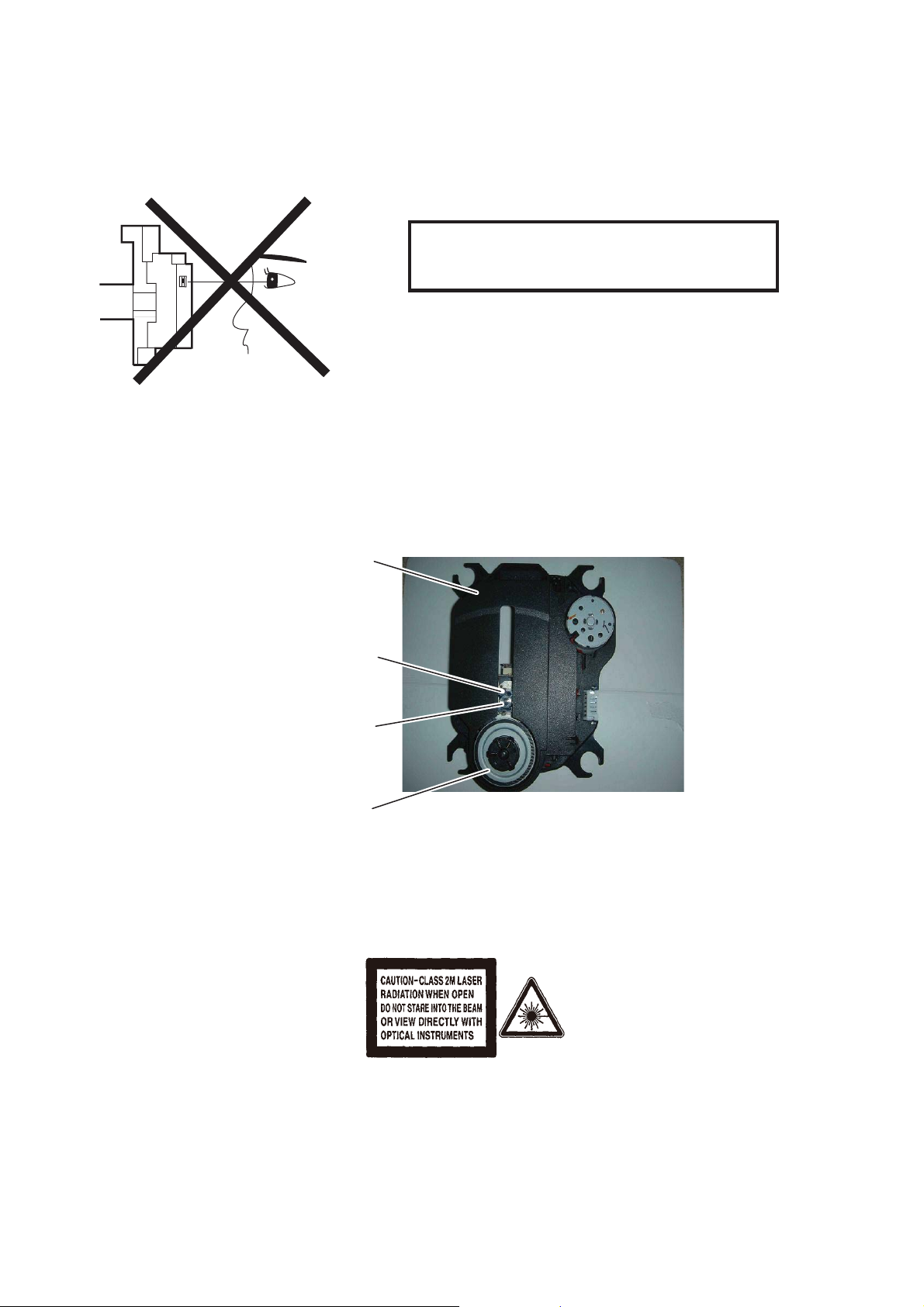
Laser Beam Safety Precautions
This Blu-Ray player uses a pickup that emits a laser beam.
Do not look directly at the laser beam coming
from the pickup or allow it to strike against your
skin.
The laser beam is emitted from the location shown in the figure. When checking the laser diode, be sure to keep
your eyes at least 30 cm away from the pickup lens when the diode is turned on. Do not look directly at the laser
beam.
CAUTION: Use of controls and adjustments, or doing procedures other than those specified herein, may result in
hazardous radiation exposure.
Drive Mechanism Assembly
Laser Beam Radiation
Laser Pickup
Turntable
Location: Inside Top of Blu-Ray mechanism.
2-1

Important Safety Precautions
Caution: These servicing instructions are for use by qualified service personnel only.To reduce the risk
of electric shock do not perform any servicing other than that contained in the operating
instructions unless you are qualified to do so.
Important
Read and understand all instructions before you use
your home theater. If damage is caused by failure to
follow instructions, the warranty does not apply.
Safety
Riskof electricshock or fire!
Neverexposetheproductand
accessories to rain or water. Never place
liquid containers, such as vases, near the
product. If liquids are spilt on or into the
product, disconnect it from the power
outlet immediately. Contact Philips
Consumer Care to have the product
checked before use.
Never place the product and accessories
near naked
including direct sunlight.
Never insert objects into the ventilation
slots
or other openings on the product.
Where the mains plug or an appliance
coupler is used as the disconnect device,
the disconnect device shall remain readily
operable.
Disconnect the product from the power
outlet before lightning storms.
When you disconnect the power cord,
always pull the plug, never the cable.
Riskof short circuit or
Before you connect the product to the
poweroutlet,ensurethatthepower
voltage matches the value printed on the
back or bottom of the product. Never
connec
if the voltage is different.
Risk of injury or damage to the home theater!
For wall-mountable products, use only
the supplied wall mount bracket. Secure
the wall mount to a wall that can support
the combined weight of the product
and the wall mount. Koninklijke Philips
Electronics N.V. bears no responsibility
for improper wall mounting that results in
accident, injury or damage.
ames or other heat sources,
re!
ttheproducttothepoweroutlet
For speakers with stands, use only the
supplied stands. Secure the stands to
the speakers tightly. Place the assembled
stands on flat, level surfaces that can
support the combined weight of the
speaker and stand.
Never place the product or any objects
on power cords or on other electrical
equipment.
If the product is transported in
temperatures below 5°C, unpack the
product and wait u
matches room temperature before
connecting it to the power outlet.
Visible and invisible laser rad
open. Avoid exposure to beam.
Do not touch the disc optical lens inside
the disc compartment.
Risk of overheating!
Never install this product in a confined
space. Always leave a space of at least
four inches around the product for
ventilation. Ensure curtains or other
objects never cover the ventilation slots
on the product.
Risk of contamination!
Do not mix batteries (old and new or
carbon and alkaline,
Remove batteries if they are exhausted
or if the remote control is not to be used
for a long time.
Batteries contain chemical substances,
they should be disposed of properly.
ntil its temperature
iation when
etc.).
Product care
Do not insert any objects other than discs
into the disc compartment.
Do not insert warped or cracked discs
into the disc compartment.
Remove discs from the disc compartment
ifyouarenotusingtheproductforan
extended period of time.
Only use microfiber cloth to clean the
product.
3-1

Important Safety Precautions
Disposal of your old product and
batteries
Your product is designed and manufactured
with high quality materials and components,
which can be recycled and reused.
When this crossed-out wheeled bin symbol
is attached to a product it means that the
product is covered by the European Directive
2002/96/EC.Pleaseinformyourselfaboutthe
local separate collection system for electrical
and electronic products.
Please act according to your local rules and
do not dispose of your old products with your
normal household waste.
Corr
ect disposal of your old product helps to
prevent potential negative consequences for
the environment and human hea
lth.
Your product contains batteries covered by
the European Directive 2006/66/EC, which
cannot be disposed with normal household
waste.
Please inform yourself about the local rules
on separate collection of batteries because
correct disposal helps to prevent negative
consequences for the environmental and
human health.
3-2

Safety Check after Servicing
Examine the area surrounding the repaired location for damage or deterioration. Observe that screws, parts, and
wires have been returned to their original positions. Afterwards, do the following tests and confirm the specified
values to verify compliance with safety standards.
1. Clearance Distance
When replacing primary circuit components, confirm
specified clearance distance (d) and (d’) between
soldered terminals, and between term
surrounding metallic parts. (See Fig. 1)
Table 1: Ratings for selected area
inals and
Chassis or Secondary Conductor
Primary Circuit
AC Line Voltage Clearance Distance (d), (d
110V~220V
Note
: This table is unofficial and for reference only. Be
sure to confirm the precise values.
3.2 mm (0.126 inches)
’)
2. Leakage Current Test
Confirm the specified (or lower) leakage current
between B (earth ground, power cord plug prongs) and
externally exposed accessible parts (RF terminals,
antenna terminals, video and audio input and output
terminals, microphone jacks, earphone jacks, etc.) is
than or equal to the specified value in the table
lower
below.
Measuring Method (Power ON):
Insert load Z between B (earth ground, power cord plug
prongs) and exposed accessible parts. Use an AC
eter to measure across the terminals of load Z.
voltm
See Fig. 2 and the following table.
d' d
Fig. 1
Exposed Accessible Part
Z
AC Voltmeter
(High Impedance)
Earth Ground
B
Power Cord Plug Prongs
Table 2: Leakage current ratings for selected areas
AC Line Voltage Load Z Leakage Current (i) Earth Ground (B) to:
110V~220V
Note: This table is unofficial and for reference only. Be sure to confirm the precise values.
0.15 µF CAP. & 1.5 k
Connected in parallel
RES.
i
0.5 mA Peak Exposed accessible parts
4-1
Fig. 2

Safety Information, General Notes & Lead Free Requirements
1 Safety Instructions
1.1 General Safety
Safety regulations require that during a repair:
Connect the unit to the mains via an isolation transformer.
Replace safety components, indicated by the symbol
only by components identical to the original ones. Any
other component substitution (other than original type)
Safety regulations require that after a repair, you must return
the unit in its original condition. Pay, in particular, attention to
the following points:
Route the wires/cables correctly
mounted cable clamps.
damage.
Check the electrical DC resistance between the mains
plug and the secondary side:
1. Unplug the mains cord, and connect a wire between
the two pins of the mains plug.
2. Set the mains switch to the ‘on’ position (keep the
mains cord unplugged!).
3. Measure the resistance value between the mains
plug and the front panel, controls, and chassis
bottom.
4. Repair or correct unit when the resistance
5. Verify this, before you return the unit to the customer/
user (ref. UL-standard no. 1492).
6. Switch the unit ‘off’, and remove the wire between the
two pins of the mains plug.
1.2 Laser Safety
This unit employs a laser
may remove the cover, or attempt to service this device (due
to possible eye injury).
2 Warnings
2.1 General
All ICs and many other semiconductors are susceptible to
,
during repair can reduce life drastically. Make sure that,
during repair, you are at the same potential as the mass
of the set by a wristband with resistance. Keep
components and tools at this same potential.
Available ESD protection equipment:
– Complete kit ESD3 (small tablemat, wristband,
4822 310 10671.
– Wristband tester 4822 344 13999.
Be careful during measurements in the live voltage
section. The primary side of the power supply, including
the heatsink, carries live mains voltage when you
connect the player to the mains (even when the
player is ‘off’!). It is possible to touch copper tracks and/
or components in this unshielded primary area, when
you service the player. Service personnel must take
precautions to prevent touching this area or components
in this area. A ‘lightning stroke’ and a stripe-marked
printing on the printed wiring board, indicate the primary
side of the power supply.
Never replace modules, or components, while the unit is
‘on’.
2.2 Laser
The use of optical instruments with this product, will
Only quali ed service personnel may remove the cover or
attempt to service this device, due to possible eye injury.
Repair handling should take place as much as possible
with a disc loaded inside the player.
T
shield:
electrostatic discharges (ESD,
). Careless handling
Laser Device Unit
epyT
:AIGalnN(BD)
:AIGalnP(DVD)
: AIGalnP(CD)
Wavelength : 650 nm (DVD)
)DC/DCV(mn087:
405nm(BD):
Output Power : 20 mW
)gnitirwWR+DVD(
Wm8.0:
)gnidaerDVD(
Wm3.0:
)gnidaerDC/DCV(
Beam divergence : 60 degree
CLASS 1
LASER PRODUCT
1-2erugiF
Note: Use of controls or adjustments or performance of
procedure other than those speci
ed herein, may result in
A
CAUTION VISIBLE AND INVISIBLE LASER RADIATION WHEN OPENAVOID EXPOSURE TO BEAM
ADVARSEL SYNLIG OG USYNLIG LASERSTRÅLING VED ÅBNING UNDGÅ UDSÆTTELSE FOR STRÅLING
ADVARSEL SYNLIG OG USYNLIG LASERSTRÅLING NÅR DEKSEL ÅPNES UNNGÅ EKSPONERING FOR STRÅLEN
VARNING SYNLIG OCH OSYNLIG LASERSTRÅLNING NÄR DENNA DEL ÄR ÖPPNAD BETRAKTA EJ STRÅLEN
VARO!AVATTAESSA OLET ALTTIINA NÄKYVÄLLE JA NÄKYMÄTTÖMÄLLE LASER SÄTEILYLLE. ÄLÄ KATSO SÄTEESEEN
VORSICHT SICHTBARE UND UNSICHTBARE LASERSTRAHLUNG WENNABDECKUNG GEÖFFNET NICHT DEM STRAHL AUSSETSEN
DANGER VISIBLE AND INVISIBLE LASER RADIATION WHEN OPENAVOID DIRECT EXPOSURE TO BEAM
ATTENTION RAYONNEMENT LASER VISIBLE ET INVISIBLE EN CAS D’OUVERTURE EXPOSITION DANGEREUSE AU FAISCEAU
Figure 2-2
5-1

Standard Notes for Servicing, Lead Free Requirements & Handling Flat Pack IC
Circuit Board Indications
1. The output pin of the 3 pin Regulator ICs is
indicated as shown.
Top View
Out
2. For other ICs, pin 1 and every fifth pin are
indicated as shown.
Pin 1
3. The 1st pin of every male connector is indicated as
shown.
Pin 1
Input
In
Bottom View
5
10
Instructions for Connectors
1. When you connect or disconnect the FFC (Flexible
Foil Connector) cable, be sure to first disconnect
the AC cord.
2. FFC (Flexible Foil Connector) cable should be
inserted parallel into the connector, not at an
angle.
FFC Cable
Connector
CBA
* Be careful to avoid a short circuit.
Pb (Lead) Free Solder
When soldering, be sure to use the Pb free solder.
Information about lead-free soldering
Philips CE is producing lead-free sets from 1.1.2005
onwards.
IDENTIFICATION
Regardless of special logo (not always
indicated)
One must treat all sets from
onwards, according to the next rule:
Serial Number gives a 14-digit. Digit 5&6 shows the
YEAR, and digit 7&8 shows the WEEK.
So from onwards=from 1 Jan 2005 onwards
0501
Important note : In fact also products of year 2004
must be treated in this way as long as you avoid
mixing solder-alloys (leaded/ lead-free). So best to
always use SAC305 and the higher temperatures
belong to this.
Due to lead-free technology some rules have to be
respected by the workshop during a repair:
Use only lead-free solder alloy Philips SAC305 with
order code 0622 149 00106. If lead-free solderpaste is required, please contact the manufacturer
of your sol
paste within workshops should be avoided because
paste is not easy to store and to handle.
Use only adequate solder tools applicable for lead-
free solder alloy. The solder tool must be able
To reach at least a solder-temperature of 400°C,
To stabilize the adjusted temperature at the solder-
tip
To exchange solder-tips for different applications.
Adjust your solder tool so that a temperature around
360°C
solder joint. Heating-time of the solder-joint should
not exceed ~ 4 sec. Avoid temperatures above
400°C otherwise wear-out of tips will rise drastically
and flux-fluid will be destroyed. To avoid wear-out of
tips switch off un-used equipment, or reduce heat.
Mix of lead-free solder alloy / parts with leaded
solder alloy / parts is possible but PHILIPS
recommends strongly to avoid mixed solder alloy
types (leaded
If one cannot avoid or does not know whether
product is lead-free, clean carefully the solder-joint
from old solder alloy and re-solder with new solder
alloy (SAC305).
Use only original spare-parts listed in the ServiceManuals. Not listed standard-material (commodities)
has to be purchased at external companies.
der-equipment. In general use of solder-
- 380°C is reached and stabilized at the
and lead-free).
1 Jan 2005
6-1

Standard Notes for Servicing, Lead Free Requirements & Handling Flat Pack IC
Special information for BGA-ICs:
- always use the 12nc-recognizable soldering
temperature profile of the specific BGA (for desoldering always use the lead-free temperature
profile, in case of doubt)
- lead free BGA-ICs will be delivered in so-called
'dry-packaging' (sealed pack including a silica gel
pack) to protect the IC against moisture. After
opening, dependent of MSL-level seen on indicatorlabel in the bag, the BGA-IC possibly still has to be
baked dry. (MSL=Moisture Sensit
will be communicated via AYS-website.
Donotre-useBGAsatall.
For sets produced before 1.1.2005 (except products
of 2004), containing leaded solder-alloy and
components, all needed spare-parts will be available
till the end of the service-period. For repair of such
sets nothing changes.
On our website
www.atyourservice.ce.Philips.com
information to:
BGA-de-/soldering (+ baking instructions)
Heating-profiles of BGAs and other ICs used in
Philips-sets
You will find this and more technical information within
the “magazine”, chapter “workshop news”.
For additional questions please contact your local
repair-helpdesk.
ivity Level). This
you find more
How to Remove / Install Flat Pack-IC
1. Removal
With Hot-Air Flat Pack-IC Desoldering Machine:
1. Prepare the hot-air flat pack-IC desoldering
machine, then apply hot air to the Flat Pack-IC
(about 5 to 6 seconds). (Fig. S-1-1)
Fig. S-1-1
2. Remove the flat pack-IC with tweezers while
applying the hot air.
3. Bottom of the flat pack-IC is fixed with glue to the
CBA; when removing entire flat pack-IC, first
soldering iron to center of the flat pack-IC and heat
up. Then remove (glue will be melted). (Fig. S-1-6)
4. Release the flat pack-IC from the CBA using
tweezers. (Fig. S-1-6)
apply
CAUTION:
1. The Flat Pack-IC shape may differ by models. Use
an appr
machine, whose shape matches that of the Flat
Pack-IC.
2. Do not supply hot air to the chip parts around the
flat pack-IC for over 6 seconds because damage
to the chip parts may occur. Put masking tape
around the flat pack-IC to protect other parts from
damage. (Fig. S-1-2)
opriate hot-air flat pack-IC desoldering
6-2

Standard Notes for Servicing, Lead Free Requirements & Handling Flat Pack IC
3. The flat pack-IC on the CBA is affixed with glue, so
be careful not to break or damage the foil of each
pin or the solder lands under the IC when
removing it.
Hot-air
Flat Pack-IC
Desoldering
CBA
Masking
Tape
Machine
Flat Pack-IC
Tweezers
Fig. S-1-2
With Soldering Iron:
1. Using desoldering braid, remove the solder from
all pins of the flat pack-IC. When you use solder
flux which is applied to all pins of the flat pack-IC,
you can remove it easily. (Fig. S-1-3)
Flat Pack-IC
Desoldering Braid
4. Release the flat pack-IC from the CBA using
tweezers. (Fig. S-1-6)
With Iron Wire:
1. Using desoldering braid, remove
all pins of the flat pack-IC. When you use solder
flux which is applied to all pins of the flat pack-IC,
you can remove it easily. (Fig. S-1-3)
2. Affix the wire to a workbench or solid mounting
point, as shown in Fig. S-1-5.
3. While heating the pins using a fi
iron or hot air blower, pull up the wire as the solder
melts so as to lift the IC leads from the CBA
contact pads as shown in Fig. S-1-5.
4. Bottom of the
CBA; when removing entire flat pack-IC, first apply
soldering iron to center of the flat pack-IC and heat
up. Then remove (glue will be melted). (Fig. S-1-6)
5. Release the flat pack-IC from the CBA using
tweezers. (Fig. S-1-6)
Note: When using a soldering iron, care must be
taken to
being held by glue. When the flat pack-IC is
removed from the CBA, handle it
because it may be dama
flat pack-IC is fixed with glue to the
ensure that the flat pack-IC is not
the solder from
ne tip soldering
gently
ged if force is applied.
Hot Air Blower
Soldering Iron
Fig. S-1-3
2. Lift each lead of the flat pack-IC upward one by
one, using a sharp pin or wire to whic
not adhere (iron wire). When heating the pins, use
a fine tip soldering iron or a hot air de
machine. (Fig. S-1-4)
h solder will
soldering
Sharp
Pin
Fine Tip
Soldering Iron
3. Bottom of the flat pa
CBA; when removing entire flat pack-IC, first apply
soldering iron to center of the flat pack-IC and heat
up. Then remove (glue will be melted). (Fig. S-1-6)
ck-IC is fixed with glue to the
Fig. S-1-4
6-3
To Solid
Mounting Point
CBA
Tweezers
or
Iron Wire
Soldering Iron
Fig. S-1-5
Fine Tip
Soldering Iron
Flat Pack-IC
Fig. S-1-6

Standard Notes for Servicing, Lead Free Requirements & Handling Flat Pack IC
2. Installation
1. Using desoldering braid, remove the solder from
the foil of each pin of the flat pack-IC on the CBA
so you can install a replacement flat pack-IC more
easily.
2. The “
(See Fig. S-1-7.) Be sure this mark matches the 1
on the PCB when positioning for installation. Then
presolder the four corners of the flat pack-IC. (See
Fig. S-1-8.)
3. Solder all pins of the flat pack-IC. Be sure that
none of the pins have solder bridges.
” mark on the flat pack-IC indicates pin 1.
Example :
Pin 1 of the Flat Pack-IC
is indicated by a " " mark.
Fig. S-1-7
Instructions for Handling Semiconductors
Electrostatic breakdown of the semi-conductors may
occur due to a potential difference caused by
electrostatic charge during unpacking or repair work.
1. Ground for Human Body
Be sure to wear a grounding band (1 M ) that is
properly grounded to remove any static electricity that
may be charged on the body.
2. Ground for Workbench
Be sure to place a conductive sheet or copper plate
with proper grounding (1 M
other surface, where the semi-conductors are to be
placed. Because the static electricity charge on
clothing will not escape through the body grounding
band, be
with your clothing.
careful to avoid contacting semi-conductors
<Incorrect>
) on the workbench or
CBA
Presolder
Flat Pack-IC
Fig. S-1-8
<Correct>
1M
CBA
Grounding Band
1M
CBA
Conductive Sheet or
Copper Plate
6-4

Direction of Use
*The following excerpt of the DFU/QSG serves as an introduction to the set.
The Complete Direction for Use can be download in different languages from
the internet site of Philips Customer care Center : www.support.philips.com
Overview of the main unit
a
b
c
d
e
f
l
m
n
o
a
• Turn on the device.
• Switch to standby mode or Eco
Power standby mode.
b SRC
• Select a source.
c
/
• Skip to the previous/next track.
• Search for radio stations.
• Select programmed radio station.
• Adjust time.
d
• Star t or pause play.
j Disc compartment
k
• Open or close the disc compar tment.
l COAXIAL (DIGITAL OUT)
k
j
i
h
g
t
s
r
q
p
• Digital out jack.
m HDMI (DIGITAL AV OUT)
• Connect an HDMI cable.
n AC MAIN~
• Power supply socket.
o SPEAKER OUT
• Connect speakers.
p LINE OUT
• Connect audio cables.
q DOCKING
• Connect docking device.
r FM ANTENNA
• Improve FM reception
s AUX-IN
• Connect an external audio device.
t VIDEO (VIDEO OUT)
• Video output jack.
e
• Stop play.
• Erase a programmed radio station.
• In standby mode, activate or deactivate
demonstration mode.
f
• USB socket.
g MP3 LINK
• Jack for an external audio device.
h
• Headphone socket.
i VOLUME
• Adjust volume.
• Adjust time.
7-1

Overview of remote control
a
b
c
d
e
f
g
h
i
j
k
l
m
a
• Turn on the device.
• Switch to standby mode or Eco
Power standby mode.
b DISC / RADIO / DOCK / USB / MP3-
LINK/AUX
• Select a source.
c A-B
• Repeat a specific section within a
track/chapter.
d DISC MENU
• Access the main menu of the disc.
e
/ / / ( / )/ OK
• Navigate through the menus.
• Press
• Press
/ to slow backward/forward.
/ to select programmed
radio stations in tuner mode.
• Press
/ / / to rotate a picture
during slideshow.
• Press
/ ( / ) to fast
backward/forward.
• Long press
( ZOOM) to zoom in/
out.
• Press OK to aselectionconfirm or
entry.
n
o
p
q
r
s
t
u
v
w
x
Direction of Use
f
• Return to previous display menu.
• In dock mode, enter the menu list.
g
/
• Skip to previous or next title, chapter,
• In tuner mode, select programmed
h
• Star t, pause, or resume play.
i CLOCK
• Set the clock.
j AUDIO
• Select an audio language or channel.
k VOL +/-
• Adjust the volume.
• Adjust the time.
l SUBTITLE
• Select a subtitle language.
m PROGRAM
• Program radio stations.
n DIM
• Select different levels of brightness.
o MODE
• In DISC/USB mode, select repeat play
• In DOCK mode, select repeat play
p
• Open or close the disc compar tment.
q SYSTEM MENU
• Go to the system menu.
r RDS/INFO
• Show RDS information (not applicable
• Show the disc information such as title,
s
• Stop play.
• Erase a programed radio station.
• Activate/deactivate the demonstration
t TIMER/SLEEP
• Set alarm timer.
• Set sleep timer.
u
• Mute or restore volume.
v TREBLE/BASS
• Increase/decrease the treble/bass level.
w Numeric buttons
• Select a title/chapter/track to play.
• Select a preset number.
x LOUDNESS
• Turn on/off loudness control.
BACK
track,or
file.
radio stations.
or random play.
only.
for this model).
chapter, subtitle, time elapsed, total
time, etc.
mode.
7-2

Direction of Use
3 Connect
Place the unit
1 Place the DVD micro theater near TV.
2 Place the left and right speakers at equal
distance from the TV and at an angle
of approximately 45 degrees from the
listening position.
3 Release the socket flap.
ab c
L
R
Note
To avoid magnetic interference or unwanted noise,
•
never place this apparatus and speakers too close to
any radiation devices.
• Place this unit on top of a table or mount it on the wall.
• Never place this unit in an enclosed cabinet.
• Install this unit near the AC outlet where the AC power
plug can be easily reached.
Connect speakers
Note
Ensure that the colors of the speaker wires and
•
terminals are matched.
• For optimal sound, use the supplied speakers only.
• Connect only speakers with impedance that is the
same or higher than the supplied speakers. Refer to the
Specifications
1 Hold downthe socket flap.
2 Insert the stripped part of the wire
completely.
• Inser t the right speaker wires to "R",
• Inser t the red wires to "+ ", white wires
section of this manual.
left speaker wires to " L ".
to "-".
Connect FM antenna
Tip
For optimal reception, fully extend and adjust the
•
position of the antenna.
• For better FM stereo reception, connect an outdoor
FM antenna to the FM ANTENNA jack.
• The unit does not support MW radio reception.
Connect the supplied FM antenna to the FM
ANTENNA socket on the unit.
7-3

Connect video/audio cables
Select the best video connection that the TV
can support.
• Option 1: Connect to the HDMI jack (for
an HDMI, DVI or HDCP-compliant TV).
• Option 2: Connect to the composite
video jack (for a standard TV).
Option 1: HDMI jack
Connect an HDMI cable (not supplied) to:
• the HDMI (DIGITAL AV OUT) jack on this
product.
• the HDMI input jack on the TV.
Tip
If the TV has a DVI connector only, connect via an
•
HDMI/DVI adaptor. Connect an audio cable for sound
output.
• If this product connects to a TV compatible with 1080p
or 1080p/24Hz, Philips recommends HDMI category
2 cable, also known as High Speed HDMI cable, for
optimal video and audio output.
• This type of connection provides the best picture
quality.
Direction of Use
Connect a coaxial cable (not supplied) to:
• the COAXIAL (DIGITAL OUT) jack on
this unit.
• the COAXIAL/DIGITAL input jack on the
device.
Connect the audio cables to:
• the LINE OUT-L/R jacks on this unit.the
AUDIO input jacks on the device.
LINE OUT
L
R
Route audio from other devices
Route audio from TV or other devices
Use this product to play audio from the TV or
other device such as a cable box.
Press MP3-LINK/AUX to select the audio
output of your connection.
L LINE IN R
Option 2: Composite video jack
Connect a composite video cable to:
• the VIDEO (VIDEO OUT) jack on this unit.
• the VIDEO input jack on the TV.
Tip
The video input jack on the TV might be labeled as A/V
•
IN, VIDEO IN, COMPOSITE or BASEBAND.
Route audio to other devices
You can route the audio from this product to
other devices.
Connect an HDMI cable (not supplied) to:
• the HDMI (DIGITAL AV OUT) jack on this
unit.
• the HDMI jack input jack on the device.
Tip
The HDMI connection provides the best audio quality.
•
Connect an external device
You can listen to an audio player through this
unit.
Connect the MP3 link cable to
• the MP3 LINK jack of this unit
• the audio output jack (usually headphone
jack) of the external device.
Connect power
Caution
Risk of product damage! Ensure that the power supply
•
voltage corresponds to the voltage printed on the back
or the underside of the unit.
• Before connecting the AC power cord, ensure you have
completed all other connections.
Connect the AC power cord to:
• the power socket on the back of the unit.
• the wall outlet.
7-4

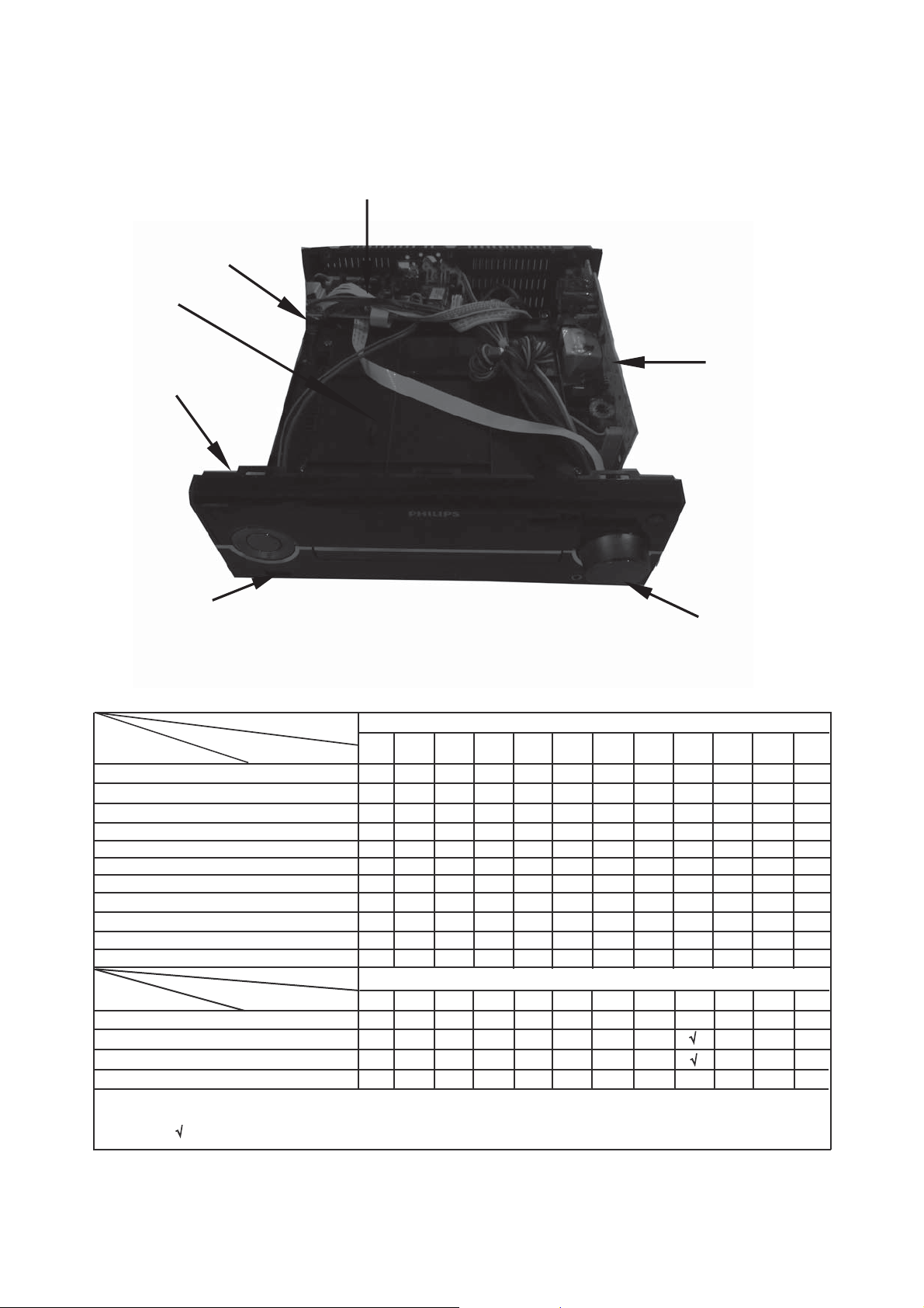
Cabinet Disassembly Instructions
1. Disassembly Flowchart
This flowchart indicates the disassembly steps to gain
access to item(s) to be serviced. When reassembling,
follow the steps in reverse order. Bend, route, and
dress the cables as they were originally.
Top Cover
[1].
Front Cover&
Display Board
Rubber Foot
Decoder Board
[2].
AMP Board
Power Board
Back Cover
AC Socket
[4].DVD Loader
A01
A01
A02
2. Disassembly Method
ID/Loc.
NO.
[1]
[2]
[3]
Part
Top Cover
Front Cover&
Display Board
Rubber Foot
Decoder Board
AMP Board
Power Board
Back Cover
AC Socket
DVD Loader
Fig.NO.
D1
D2
D3
Note:
(1) Identification (location) No. of parts in the figures
(2) Name of the part
(3) Figure Number for reference
(4) Identification of parts to be removed, unhooked,
unlocked, released, unplugged, unclamped, or
desoldered.
Axx = Screw
, CNxx/Jxx/CONxx = Connector
D3.5X12BA is specification of screw.
* = Unhook, Unlock, Release, Unplug, or Desolder
e.g. 7(A01) = seven Screws
Removal
Remove/Unhook
/Unlock/Release/
Unplug/Desolder
11(A01)D3 X 10 FA
4(A02)D3 X 10 BTH
4(A03)D3 X 8 PA
10(A04)D3 X 10 FA
1(A05)D3 X 10 BTH
4(A06)D3 X 8 BA
Note
Fig. D1
Fig. D2
A03
A04
A04
A03
A06
A05
A06
8-1
Fig. D3

Troubleshooting
FLOW CHART NO.1
No sound from whole unit
No
check if speaker is ok
check and change speaker and output wire
Yes
check if public circuit of whole unit
AMP circuit is ok
No
check radio tube and periphery circuit
Yes
check if power supply circuit of whole
unit is ok
No
check and change transormer of power supply and
power commutate circuit
Yes
check staic noisy circuit CPU circuit and change components
FLOW CHART NO.2
no sound from radio
check if output of radio is normal
No
Yes
check radio controlled circuit
No
Yes
check if power supply of radio is
normal
No
Yes
check if radio circuit components of around
it is normal
FLOW CHART NO.3
no sound from DVD
check if DVD output is normal
Yes
check if DVD controlled circuit is ok
check public circuit and circuit of power supply
check and change the related components of radio controlled circuit
check and change related components of power supply circuit
No
check and change components of around it
No
No
check public circuit
components
check and change the related components of DVD
controlled circuit
power supply circuit and change related
Yes
check if the related components of DVD
signal channel
tie wires socket is normal
Yes
change Decoder board
check and change the related components of DVD
No
tie wires
socket
9-1

no search from DVD
check if supply +12V of Decoding board is normal
Yes
Troubleshooting
No
check steady circuit
check if laser head ass'y can light normally
No
check if tie wires of laser head ass'y
is loosen and broken
No
laser head ass'y broken
FLOW CHART NO.4
no image from DVD
check if video socket
video wire is normal
No
check and change video wire
No display from display screen
socket
Yes
Yes
Yes
Decoding board is broken
check and change good laser head ass'y
Decoding is broken
check voltage of filaments transformer
is normal
transformer is broken
No
No
check if the capacitor voltage of filaments filter is short circuit
No
check if display screen is broken
Yes
change display screen
No
check if tie wire is broken
Yes
change tie wires
Yes
change capacitance
9-2

Block Diagram
M5V
IR
VFD Display
HL-1337WA
(refer to DCM713)
KEY SCAN
KEY
Tact switches X 7
LED_STBY_RED
DETECT
IDENTIFY
549K
Iphone Identify
3
3
1
2
2
AC
STBY < 0.15W
(POW2200A/B)
refer to MCM7000
IR
1
*
EXTERNAL DOCK
IPHONE
VFD5V
VF1
VF2
-27V
Transformer1
Transformer2
Transformer3
PICK UP SONY
DM-06BXL X-L2
DVD Loader
HOST USB 2.0
TRAY MOTOR+/-
M
___
CD DOOR
TRAY SW
D5V
VFD Driver
PT6311
VFD
POWER
SUPPLY
UART i phone
PIN13 Iphone DET
PIN20 DETECT
PIN10 IDENTIFY
IPHONE L,R
M5V 1A
D5V 2A
12V 1A
17V AMP 4A
-27V
D5V
ECO_POW
ECO POWER
SPSP+
LIM
GND
SLSL+
VUSB
DD+
GND
MOT+
MOTGND
SW-IN
SW-OUT
STB5V
GND
IR
STB
CLK
DATA
ECOP
TXD
RXD
DET
IDEN
L
R
5V 2.1A
GND
5V
12V
29V
GND
ECOP
F-
Vc(Vref)
F+
Vcc
T+
E
T-
NC
VR-CD
C/c
VR-DVD
D/d
VR-LD
CD/DVD SW
MD
RF
HFM
A/a
NC
B/b
DVD-LD
F
GND-LD
GND-PD
MPEG_ON
APM9435
IR
FM Antenna 75OHM
IPHONE L,R
RCA(R/L)
MP3 LINK REAL
M5V
Motor Driver
5888S
MPEG5V
A5V
FM
Si4704
4705(RDS)/12/05
BUFFER
LM324
ECO_POWER
AMC1117
3.3V
LDO
1.2V
AMC1117
LDO
3.3VD5V
AMC1117
D5V
TRAY IN/OUT
MOTOR DRIVER
VFD_BUS STB,CLK,DATA
UART i phone
Iphone DET
Iphone Identify
IPHONE RING DETECT
A5V
D3.3V
Audio switch
CS5346
3.3V
USB
TRAY MOTOR+/TRAY SW
ADC
SDR_DRAM
M12L64164A
SERIAL-FLASH
EN25F16
12V5VGND
IR
RST_FM
RST_5346
IIS_PCM
IIS_ADC
D3.3V
D3.3V5V
MLK
BCK
WCK
CP
MFI341S2164
IPHONE/IPOD
EEPROM
24C02
DATA
IIC_CP
SCL
MPEG_RST
CP RST
MCU 3.3V
SDA
MPEG
MT1389DXE-G
IIC_MPEG
IIC_INT
CECIN
CECOUT
IICINT
MUTE
CDON
CDRST
IIC_INT
MPEG_ON
IIC_MPEG
SLAVER
MCU
R5F21258
MASTER
IIC AUDIO
D3.3V D1.2V
RST_9831
MUTE_9831
Audio Processor
PS9831
IIS
MCU 3.3V
MUTE
A3.3V
CVBS
COAXIAL
CEC
MUTE
CEC_IN
CEC_OUT
ECO_POWER
HP SENS
HP MUTE
FAN_AMP_CTRL
AUDIO LEVEL DETECT
AMP_OTW
RST_AMP
~MUTE
~HPMUTE
PWM HP
PWM RECOUT
PWM 4,L
PWM 3,R
REVERSE
CEC BUFFER
CEC_IN
CEC_OUT
SDOVL
D3.3V
D5V
AUDIO LEVEL
RC
line out & Headphone
RC + DRV604
A12V
POWER AMP
TAS5342L
BTL X 2
ESD REJECTOR
& EMI
A3.3V
17V
CEC
LINE OUT
Head phone 3.5mm
30W*2
COAXIAL
RCA(R/L)
Front pannel
HP SENS
CVBS
HDMI
dome tweeter
woofer
dome tweeter
woofer
(8 Ohm )
(6 Ohm )
(8 Ohm )
(6 Ohm )
10-1 10-1

Wiring Diagram
SPK Board
P1
CON3
AMP Board
CON2
STB
GND
+20V
+20V
GND
GND
+12V
D+5V
MCU+5V
MCU+5V
D+5V
D+5V
+12V
GND
GND
CON4
P8
CON5
CON6
CN2
Power Board
CON1
2.0/6P
J1
P6
P1
CN3
AC220V
2.0/5P
Display Board
CON6
P2
CON7
CON4
CN1
CN6
Decoder Board
CON1
P2
DVD Loader
J9
CN6
CN502
MUTE
GND
J502
GND
D-
D+
VCC
CN401
J401
H-R
H-L
CN501
AUX-L
AUX-R
GND
Headphone Board
J501
USB Board
11-1 11-1
CN301

AMP Board -- Circuit Diagram
FM_CP_RST
DAB_MUTE
R193 NC/330
IPOD/DAB_TX
R170
R169
R194 NC/330
L29
L30
FB/1K
FB/1K
TP35
TP44
C184 100P
TP36
TP45
FB600
AUX_INL
AUX_INR
TP38
TP37
D17
ESD/NC
TP46
TP47
2
1
R73 NC/NC/0
R74 NC/0/NC
R82 NC/NC/0
R83 0/0/NC
R100 NC/NC/NC
DCD7010
1.0/16P
3.3V/I2C_INT
CEC_INPUT
CEC_OUTPUT
HPD
GND
SDA
SCL
CD_MUTE
DVD_ON
GND
3.3V/GND/I_VIDEO_SW
M_OPEN
OPEN/CLOSE_SW
CD_TRIN
IPOD/DAB_RX
NC/0
R175 330/NC
MSCL
L59 FB/600
SCL3
R173 330/NC
MSDA
L60 FB/600
SDA3
FM_INR
FM_INL
L51
FB/1K
C186 332
12
12
1
2
D12
D18
ESD/NC
ESD/NC
C215 1000P
C191 332
C190 332
TP48
I+5V/2_1A
IGND
J4
CON2.0-4
I2C_INT/3_3V
3_3V/GND/VIDEO_SW
MBD7020
1.0/12P
I2C_INT/3.3V
CEC_INPUT
CEC_OUTPUT
HPD
GND
SDA
SCL
CD_MUTE
DVD_ONDVD_ON
RESET
GND
3.3V/GND/I_VIDEO_SW
CON1
ST-013
C187 332
12
D16
ESD/NC
C199 332
1
2
3
4
C213 332
FB13 FB/0805/120R
FB/0805/120R
2
1
L17 FB/600
FM5V
L31 NC
CB6
CE22
+
0.1uF
100uF/1OV
R242 10K
LCH_IPOD
IPOD_L_CH
IPOD_R_CH
RCH_IPOD
R246 10K
R256
R255
C197
C196
10K
10K
332
332
AGND
R244 1K
FM_INR
FM_R_CH
R248 1K
FM_INL
FM_L_CH
R260
R259
C200
C201
10K
332
332
10K
AGND
R241 10K
AUX_INR
AUX_R_CH
R245 10K
AUX_L_CH
AUX_INL
R254
R253
C195
C194
10K
10K
332
332
A5V
R209
0/0805
CE29
+
C159
100uF/10v
2.2uF
1
V+
R210 0
MP3_R_CH
C160 2.2uF
2
OUTA
C161 2.2UF
MP3_INR
3
INA
R212 2.2K
4
INT
R217
5
VREF6SENCE
C173
C176
10K
2.2UF
0.022uF
FB12
+IP5V
CN1
CON1.0-12
1
VFD-CLK
1
2
VFD-STB
2
3
VFD-DATA
3
REMOTE
4
4
GND
5
5
ROT-A/B
6
6
MCU_5V
7
7
GND
8
8
LED_PWM_VOL
9
9
10
ECO_POWER
10
11
11
12
12
TP51
TP52
TP27
TP26
TP21
TP24
TP20
TP23
TP22
TP19
TP25
CX1117-3.3
U10
MCU_5V
3
IN
C189
CE28
+
0.1uF
CD11X/220UF16V/D6.3H7
TP67
TP68
J3
TP69
CON2.0-4
TP70
1
2
J5
3
4
4
3
2
1
CON1.0-4(
)
咥㡆
3_3V_MCU
FB11
FB/0805/120R
TP59
TP58
TP57
TP56
TP55
TP54
TP53
TP50
TP49
CN6
L52 FB/1K
1
L53 FB/1K
2
L45 FB/1K
3
L44 FB/1K
4
L54 FB/1K
5
L42 FB/1K
6
L41 FB/1K
7
L40 FB/1K
8
L39 FB/1K
9
L38 FB/1K
10
L37 FB/1K
11
L36 FB/1K
12
L35 FB/1K
13
L55 FB/1K
14
L33 FB/1K
15
L32 FB/1K
16
FPC16P
6x2.0 W/HOUSING
TP66
TP60
TP65
TP61
TP64
TP62
M_BOY
TP63
12
L58
D22
FB/1K
ESD/NC
AV4-8.4-13D
P2
Pins
/RST
SEN
SCL
10
SDA
11
FM5V
12
GND
13
ROUT
LOUT
GPIO2
J2
FMZZ-9P
TUNER
6
5
4
3
2
1
1
2
3
4
5
6
7
CON7
CON2.0-7
MCU <=> MPEG
MCM7000
1.0/12P
1
2
3
4
GND
5
SDA
6
7
SCL
CD_MUTE
8
9
RESET RESET
10
GND
11
3.3V/GND/I_VIDEO_SW
12
M_CLOSE M_CLOSE
13
M_OPEN
14
OPEN/CLOSE_SW
15
CD_TRIN
16
C188
100P
1
2
3
4
5
6
7
8
9
C183 100P
LINE_OUT_L
LINE_OUT_R
GND
MP3_INR
MP3_INL
GND
HP_R
HP_L
HP-SENSHP-SENS
TP43
CON4
CON2.54-2P
IIC_INT
3_3V_MCU
3_3V_MCU
GND
VIDEO_SW
A5VMCU_5V
LCH_IPOD
RCH_IPOD
FM_L_CH
FM_R_CH
U12
D2761
10
GND
C175 2.2uF
9
OUTB
C174 2.2uF
8
INB
7
SW
R119
3.9K
FB7
GND
FB/0805/120R
C219 100P
C222 100P
C220 100P
C218 100P
C221 100P
R195 NC/NC/NC/100R
MSCL
MSDA
R207 NC/NC/NC/100R
C217 100P
C216 100P
3_3V_MCU
2
OUT1
4
OUT2
ADJ
+
SOT223
1
CE27
47uF/16V
CB8
0.1uF
I2C_INT/3_3V
CEC_INPUT
CEC_OUT
HDMI_HPD_MCU
GND
SSDA
SSCL
A_MUTE
DVD_ON
DVD_RST
GND
3_3V/GND/VIDEO_SW
M_CLOSE
M_OPEN
OPEN/CL_SW
TRIN
R179 0R/NC/NC
R180 NC/0R/NC
R184 NC/NC/0R
3_3V_VD
C142
R142
0.1uF
3_3V_VD
L56
FB/1K
MSDA
MSCL
R164 100R
CS5346_RST
C172
C171
C170 4.7UF/16V
C169 4.7UF/16V
R213 0
R215 2.2K
R216
10K
SGND
C223 100P
C225 100P
C224 100P
REMOTE
C202 100p
SSCL
DVD_ON
SSDA
R200
4.7K
R211
D15
1N4148
10K
12
C177
0.01uF
32.768KHz
XCIAN
C150
20pF
10K
R143
10K
R146
R147
C143
C144
R172
1uF
0.1uF
10K
R150 100R
R151 100R
C158
0.1uF
4.7UF/16V
4.7UF/16V
MP3_L_CH
MP3_INL
3_3V_MCU
R149 10K
R274 10K
HP-SENS
SSDA
C140 100P
L16 FB/1K
L19 FB/1K
R185 33
MODE
XCIAN
XCOUT
REST_MCU
10K
R204 10K
R203
M_OPEN
CB7 0.1uF
C178
0.01uF
Y2
XCOUT
C151
20pF
R176 330
R177 1k
R181 330
R206 1K/1K/NC
39
37NC38
40NC41
42
43
45
46
47
48
44
U7
10K
10K
NC
NC
VD
INT
SCLK
LRCK
OVFL
MCLK
DGND
SDOUT
1
SDA/CDOUT
VLS
2
NC
SCL/CCLK
3
NC
AD0/CS
4
NC
AD1/CDIN
5
VLC
AGND
6
RST
NC
7
AIN3A
NC
8
AIN3B
PGAOUTB
L34
9
AIN2A
PGAOUTA
L46
10
AIN2B
AIN6B
11
AIN1A
AIN6A
FB/1K
12
AIN1B
MICBIAS
FB/1K
AIN4B/MICIN2
AIN5B
FILT+
AIN5A
NC
VA15AFILTA
AGND
AFILTB
AIN4A/MICIN1
CS5346
23
24
18VQ19
20
22
14
16
17VQ21
13
+5V_VA
CE24
C163
C162
+
10uF/16v
222
104
C164
C165
C166
222
104
104
UCM_V3_3AV_V5+
R270
R271
R269
4.7K
NC/4.7K
3.3K
CS5346_RST
Q12
R272
D23
8050
2
2V
1K
13
Q13
12
8050
2
13
R273
1K
R55
R57
C64
33k
33k
1u
C68
R65
105
100k
IPOD_L_CH
IPOD_R_CH
C72
R67
105
100k
R183 10K
R122 10K
IPOD_ACC_PWR_DET
TRIN
R187 10K/10K/NC
PWM_RST
OTW
HDMI_HPD_MCU
AMP_PDN
R208 10K
R148 10K
FM_CP_RST
SSCL
AMP_PDN
ROT-A/B
OPEN/CL_SW
C127 104
C132 104
C203 104
C212 104/ 104/NC
R174 330/330/NC
C139 100P
R160 330
R159 100
R157 100
R158 100
52
48
50
47
51
49
AD6
AD4
AD5
SD_DET
DVD_SW
USB_DET
1
NC
2
SCLK
3
DVD_ON
4
SSDA
5
MODE
U8
6
R5F21258
XCIAN
R8C2425-LQFP52
7
XCOUT
8
RST
XOUT
9
XOUT
10
VSS
XIN
11
XIN
12
VCC
13
M_OPEN
VFD_DATA
CLOSE_SW
M_CLOSE
OPEN_SW
VFD_CLK
VFD_STB
18
14
19
16
17
15
R221 470
R227 330
R226 470
R224 330
R225 470
R234 NC/NC/33
R223 1K /1K /NC
R214 NC/NC/33
L25 FB/1K
L24 FB/1K
L26 FB/1K
USB_EN1#
CS5346_RST
HP/LINE_MUTE
M_CLOSE
VFD-DATA
USB_OC1#
VFD-CLK
VFD-STB
CON6
TO MPEG PCB
4
BCK_DVD
3
LRCK_DVD
2
DATA_DVD
1
CON2.0-4
R133 100R
R132 100R
R127 100R
R125 100R
3_3V_VD
VLS
FB8
36
35
34
33
32
31
30
29
28
27
26
25
CE21
NC/2.2uF/50v
CE25
+
47uF/16v
+12V
VCC_AMP
84
5
+
6
-
R68 220k
3_3V_MCU
FM_CP_RST
DVD_RST
R155
R162 33
R161 100
45
46
44
TREO
IPOD_SW
AD_VREF
ROTB222ROTA2
REMOTE
21
20
R229 330/NC
R228 33
R230 330
IR
12
IN60
D10
REMOTE
VIDEO_SW
HP-SENS
FB9
FB/0805/1K
C146
C145
CE20
1uF
0.1uF
+
100uF/10v
C148
+
7
104
C154 4.7UF/16V
C155 4.7UF/16V
C156 4.7UF/16V
C157 4.7UF/16V
+5V_VA
FB10
FB/0603/1K
CE26
+
C167
100uF/10V
C168
0805/4.7uF/10V
104
VCC_AMP
L9 FB
C50
+
104
U3-A
4558/SO
84
3
+
1
2
-
D2
C66
U3-B
BAS316
105
4558/SO
12
R62
R61
D3
100k
100k
BAS316
12
ROT-A/B
OPEN/CL_SW
3_3V_MCU
R152 10K
100/100/NC
R156 47K
R165 3.9K
R163
R265 100
43
41
40
42
NC
AD2
AD3
AD1
39
NC
R205 330
38
AD0
L18 FB/1K
R178 100
37
MSCL
R182 100
L20 FB/1K
36
MSDA
R186 330
35
ECO_POWER
R191 330
34
LED_CTRL
R196 330
33
MUTE_LINE
L23 FB/1K
R199 330
32
MUTE_MCU
31
STANDBY
L22 NC/FB-1K/NC
R263 NC/470/NC
30
DAB_SW
R266 330
29
TX2(ROTA3)
R267 330
28
RX2(ROTB3)
R268 330
27
ROTB1
TX1
ROTA1
RX1
NC
23
25
24
26
L21
NC/FB-1K/NC
CP_SCL
NC/100P/NC
C180
CP_SDA
R232 330
R231 330
C179
NC/100P/NC
NC/NC/470
R264
L27 FB/1K
L28 FB/1K
R233 NC/470/NC
12
IR
D11 IN60
C185
101
IPOD/DAB_TX
IPOD/DAB_RX
IIC_INT
CP_SDA
M_BOY
OTW
TO MCU
AMP_PDN
+3V3
U9
CX1117-3.3
A5V
2
3
OUT1
IN
4
OUT2
ADJ
CE30
C181
+
1
SOT223
0.1uF
C182
R235
R222
R237 10K
R236 10K
0.1uF
+3V3
MSCL
MSDA
TO MCU
PWM_RST
MCLK_AD
+3V3
C12
220uF/16V
LRCK_DVD
BCK_DVD
DATA_DVD
FB/0603/120R
FB5
C210 100P
C209 100P
C211 100P
C29
47uF/16V
FB6
FB/0603/120R
L4 FB/1K
BCK_DVD
L6 FB/1K
LRCK_DVD
DATA_DVD
L7 FB/1K
BCK_AD
LRCK_AD
DATA_AD
R51 470
MUTE_9831
1_8V_C
C118
C119
C117
103
103
103
C128
C130
C129
103
103
103
MUTE_HP/LINE
A_MUTE
MCU_MUTE
DAB_MUTE
A_MUTE
HP/LINE_MUTE
DAB_MUTE
IPOD_AUDIO_DET
R239 330
MSDA
R240 330
MSCL
MSCL
MSDA
ECO_POWER
FAN_CTRL
LED_PWM_VOL
MCU_MUTE
CP_SCL
IPOD_DET
CEC_OUT
CEC_INPUT
3_3V_MCU
NC/10K/NC
NC/10K/NC
R238 10K
220uF/10V
TP39
TP41
TP40
TP42
MCLK_AD
LRCK_AD
BCK_AD
DATA_AD
+3V3
FB/0805/1K
C147
C149
104
0805/4.7uF/10V
MP3_R_CH
MP3_L_CH
AUX_R_CH
AUX_L_CH
A5V
CE3
100uF/16V
IPOD_AUDIO_DETIPOD_AUDIO_DET
CE5
+
100uF/10V
LED_PWM_VOL
MSCL
MSDA
C152
C153
100pF
100pF
C204 100P
HP_L
TP5
TP6
RECOUT_P_R
RECOUT_M_R
LINE_OUT_R
R251
47K
PWM_HP_L_M
PWM_HP_L_P
R15 10K
R18 100
R19 100
R22
R25 100
FB4 FB/0805/120R
C20 47uF/16V
C22 104
C30
104
R64 0
R66 0
R70 0
R72 0
R167
L14
D8 1N4148
D9 1N4148
D19 1N4148
D13 1N4148
12
D14 1N4148
12
D20 1N4148
12
3_3V_MCU
+3V3
1K
C112
103
CD11X/10UF16V/D5H11
L12
C192
101
2K2
R171
10K
FB
CD11X/10UF16V/D5H11
12
12
12
SDA1
SCL1
CB9
0.1uF
+3V3
FM_CP_RST
R111
CD11X/47UF16V/D5H7
C126
220uF/16V
C110
103
C111
103
PWM_HP_R_M
PWM_HP_R_P
PWM_HP_L_M
PWM_HP_L_P
+
CE6
+
CE8
CD11X/10UF16V/D5H11
CD11X/10UF16V/D5H11
FB
2
R126 0R
CE18
CD11X/220UF16V/D5H11
+
CE14
+
CE16
CD11X/10UF16V/D5H11
0/0805
R5100K
C4
22P
C11
104
IO_VSS
1
PLL_DVSS
2
PLL_DVDD
3
IO_VDD
4
IO_VSS
5
PLL_AVDD
6
IO_VSS
7
PLL_AVSS
8
IO_VSS
9
IO_VDD
10
MBCK
11
MLRCK
12
DVDD
13
DVSS
14
MSDIN0
15
MSDIN1
16
MSDIN2
17
MSDIN3
18
SBCK
19
SLRCK
20
IO_VSS
21
IO_VDD
22
SSDIN0
23
SSDIN1
24
SSDIN2
25
GND
1_8V_C
IO_VDD_C
C62
+
104
220uF/16V
C69
330P
R87 6.8K
R93 6.8K
CE11
LINE_O_R
+
A5V
R154
10K
ZER0_LINE_OUT
Q11
2N3904
13
HP_LAA
+
R128 6.8K
R134 6.8K
R197 470
U11
24C02
VSS5SDA
6
SCL
A2
7
TEST
A1
8
VDD
A0
R97
100
+
CE12
CB5
0.1uF
+3V3
C5
Y1
*12.288MHz
22P
R11
R13
R12
100
10K
10K
R27
R26
R28
10K
10K
R24
10K
10K
86
84
87
82
79
80
81
76
97
99
83
85
88
90
89
91
77
78
100
94
92
93
95
96
X_IN
DVSS
DVSS
DVDD
DVDD
X_OUT
SP_I2C
IO_VSS
IO_VDD
IO_VSS
NRESET
SCK_SCL
EPD_ENA
DMIX_BCK
SCAN_ENA
OVERLOAD
SI_I2C_AD0
DMIX_LRCK
IO_SO_SDA
DMIX_MCLK
DMIX_SDOUT
TEST_MODE198TEST_MODE2
TEST_MODE3
N_CS_I2C_AD2
U2
PS9831
RECOUT_P
RECOUT_M
DVSS
PWM_HP_LEFT_M46PWM_HP_LEFTF_P47IO_VDD48RECOUT_M
MIC_LRCK
DVDD
RECOUT_P50IO_VSS
EXT_MUTE28IO_VSS29IO_VDD30MIC_MCLK31MIC_BCK
DVDD
IO_VSS
SSDIN3
DVSS36PWM_SW_LINE_M37PWM_SW_LINE_P38IO_VSS39IO_VDD40PWM_HP_RIGHT_M41PWM_HP_RIGHT_P
MIC_SDIN
42
43
45
49
27
44
32
33
34
35
26
close 29pin close 39pin
C113
C114
C125
close 47pin
103
103
C61
104
C63
470uF/16V
R63 15K
R71 15K
R75 15K
R80 15K
C73
C70
C74
R105
R104
330P
330P
330P
R108
R106
10K
10K
10K
10K
R84
C83
150P
C91
100pF/J
C214
0.1uF
C115
1000pF
C135
330pF/J
R138
18K
4
3
2
1
MCU
1
2
3
4
5
C79 2.2uF
U6
C81
33K
56P
1
R88 33K
+LD_L
2
R94 33K
-LD_L
C85
56P
3
R101 33K
OUT_LDL
R103 47R
4
AGND
ZER0_LINE_OUT
5
EN_LD
C95 1uF
6
PVSS_LD
7
CN_LD
8
CN_HP
C101 10uF/10V/0805
9
PVSS_HP
10
EN_HP
R120 1R
11
AGND
R123 18K
12
OUT_HPL
C133
R129 47K
82P
13
-HP_L
R135 47K
14
+HP_L15+HP_R
DRV604
C137
82P
C141 4.7uF
R198 1K
MUTE_9831
MUTE
CE23
R202
+
1UF
68K
MUTE_HP/LINE
20
21
16
19
NC19
NC20
NC1617NC1718NC18
VSS1
15
NC1
NC15
14
R86 10K
MODE0
MODE1
13
NC3
NRESET
VCC
R91 330
I2C_SDA
iPod_CP_2.0
12
R98 330
I2C_SCL
11
VSS
NC6
NC7
NC10
NC89NC9
7
8
6
10
iPod_CP_2.0(21264)
+3V3
R6
R7
4K7
4K7
100
R9
R14
2K7
Q3
1
3904
C6
32
103
C7
104
R30 NC
C124 104
close 94pin
R37 100
FR+
PWM4_P
R39 100
75
FR-
PWM4_M
74
C123 103
IO_VSS
73
IO_VDD
R42 100
72
FL+
close 73pin
PWM3_P
R43 100
71
FL-
PWM3_M
70
IO_VSS
69
PWM2_P
68
C37
C35
C34
C36
close 65pin
PWM2_M
67
DVDD
66
100P
100P
100P
100P
IO_VDD
65
IO_VSS
64
C122 103
DVSS
63
PWM1_P
62
PWM1_M
61
IO_VSS
60
NC
59
close 56pin
NC
58
IO_VSS
57
IO_VDD
56
C121
NC
55
NC
104
54
IO_VSS
53
52
51
R47 10K
L-CH-PCM:RECOUT_P1,RECOUT_M1
RECOUT_P1
R-CH-PCM:RECOUT_M,RECOUT_P
R56
10K
+
C65
104
RECOUT_M
RECOUT_M1
蝒筐
CS8415-TSSOP28
R118 15K
R110 15K
RECOUT_P
R81 15K
R92 15K
R99
R76
10K
10K
C75
330P
10K
R77
R78 22K
C77
471p
R79
6.8K
C82
R85
56P
33K
28
+LD_R
27
-LD_R
26
OUT_LDR
25
EX_UVP
24
PGND
23
PVDD_LD
22
CP_LD
21
CP_HP
20
PVDD_HP
18
NC
19
PGND
17
OUT_HPR
16
-HP_R
+3V3
CP_SDA
CP_SCL
R90 6.8K
R89 33K
C84
56P
R95 33K
R96 6.8K
C86
150P
R102 33K
R107 47R
LINE_O_L
CD11X/10UF16V/D5H11
C93
100pF/J
C96 1uF
CE13
+
CD11X/470UF16V/D5H11
C102 1uF
C116
1000P
R121 1R
CD11X/220UF16V/D5H11
R124 18K
C134
82P
R130 47K
R131 6.8K
C136
R136 47K
R137 6.8K
330pF/J
R140
C138
82P
18K
I+5V/2_1A
CB4
0.1uF/10V
IGND
C10
C9
47uF/25V
104
R31
10
U1 TAS5342L
C13 104/2012
44
1
GVDD_A
GVDD_B
R33 1K
OTW
R36 100
/SD
R41 100
AMP_PDN
R52
104
C57 104
1R/0805
C6047uF/25V
C59
RECOUT_P1_L
RECOUT_M1_L
RECOUT_M_R
RECOUT_P_R
C80
C78
C76
330P
330P
330P
A5V
CD11X/10UF16V/D5H11
CE7
+
RECOUT_P1_L
CE9
+
RECOUT_M1_L
CD11X/10UF16V/D5H11
L11
CE10
+
LINE_OUT_L
FB
C193
47K
101
R252
+3V3
L13
C100
1
1uF
R139 0
CE19
L15
+
HP_R
HP_RAA
FB
CD11X/10UF16V/D5H11
CE15
+
PWM_HP_R_M
CE17
+
PWM_HP_R_P
CD11X/10UF16V/D5H11
43
2
BST_A
/OTW
42
3
NC
NC
41
4
PVDD_A
NC
40
5
PVDD_A
/SD
39
6
OUT_A
PWM_A
38
7
GND_A
/RESET_AB
37
8
GND_B
PWM_B
R44 27k
36
9
OUT_B
OC_ADJ
35
10
PVDD_B
GND
34
11
BST_B
AGND
C39 104
33
12
BST_C
VREG
32
13
PVDD_C
M3
31
14
OUT_C
M2
30
15
GND_C
M1
29
16
GND_D
PWM_C
28
17
OUT_D
/RESET_CD
27
18
PVDD_D
PWM_D
26
19
PVDD_D
NC
25
20
NC
NC
21
VDD24BST_D
23
22
GVDD_D
GVDD_C
10R
R53
10(3)
R54
C
1
2
3
U4
IN
GND
EN#4FAULT#
A5V
3_3V_MCU
R50 10K
USB_OC1#
TPS2553DBVT
6
+IP5V
OUT
5
ILIM
CE4
R58
+
R59
CB3
510
20K
100uF/10V
0.1uF/10V
R0603/SMD
IGND
A5V
USB_EN1#
R60
10K
MARK2
MARK4
MARK1
MARK3
+12VP25V
+
CE1
CD11X/100UF16V/D6.3H7
FB1
FB/0805/120R
R2
C1
C2
3.3
CD263/1000uF/35V
104
CB1
CB2
104
103
R29
10
C14
104
L43
C15 680PF
C17 333
C38 333
C40 333
C55 333
C58
104(2)
FB100/5A
C19
XXX->470P
C25
C26
224(2)
XXX->470P
C32
224(2)
C43
224(2)
C49 224(2)
FAN_CTRL
FRO-
FRO+
FLO+
FLO-
C31 680PF
L47
FB100/5A
FB100/5A
L48
C41 680PF
C45
XXX->470P
C51
XXX->470P
L49
FB100/5A
C54 680PF
P25V
C67
103
C71
104
R69
3.3
R3
1K
R4
1K
Q2
2
8050
C3
13
0.1uF
22K
R10
2
13
12
Q4
R16 12K
D1
8550,DIP
1N4148
8550,DIP
R21
R23 12K
Q6
10K
13
2
R32
22K
MODEL
MCM7000 DCD7010 MBD7020
ITEM
R179-0R
Y
R180-0R
R184-0R
NC NC
CN2-DIN9 Y NC Y
CON2-1.0/8P NC Y NC
CIRCUIT A NC Y NC 㕂DOCKˈCP㕂DŽ
R214,R234-33 NC NC Y
L21,L22-FB/1K
R233,263-470
NC Y NC
R222,235-10K
C179,C180-100P
R163-100
YYNC
C212-104
R187-10K
CN1 1.0/10P 1.0/10P 1.0/10P 1.0/12P
R195,R207-100 NC NC NC Y㽕TOUCH KEY
CIRCUIT C Y Y Y NC NE1508D ᮴HEADPHONE
CON7 2.0/7P 2.0/7P 2.0/7P 2.0/4P NE1508D ᮴MP3 linkࡳ㛑DŽ
CON4-2.5/2P
FB12,FB13-FB/120
R73 NC NC
R74
R82
R83
R100
ࠡ4Pinぎ) 1.0/16P
CN6 1.0/12P(
C16 104
R34
10R
R38
10R
R45
10R
R48
10R
H1
SYP580
R1
47K
R20
22K
+12V
2
L1
10uH5A
10uH5A
L2
L8 10uH5A
10uH5A
L10
13
Q1
8550,DIP
R8
2
+
C8
100UF16V/D6.3H7
C21 104
C27 104
C33 104
C42 104
C46 104
C52 104
C56 104
P25V
C231 104
FB2
FB/0805/33R
4.7 1W
CE2
+
100UF16V/D6.3H7
FB3
FB/0805/33R
Q5
R17
8050,DIP
82/1W
13
NC NC
Y
R35
6.2R
R40
6.2R
R46
6.2R
R49
6.2R
YNCNC
YNCY
1.0/12P(ৢ4Pinぎ)
C18 102
CBB
C24
C23 102
474
C28 102
L3
TC0903-100UH 3A
3
FRO+
TP1
TP2
TP3
TP4
C44 102
CBB
C47 102
C48 474
C53 102
CON3
TO POWER PCB
A5V
ECO_POWER
+12V
P25V
MCU_5V
CON2.54-9
C205 102
C206 102
C207 102
C208 102
C230 104
J1
CON2.54-2
1
2
NE1508D
NC
CNCN
NC
Y
NC
NC
Y
Y
NC
CNK1-322R,602R DBMYY
Y
NC
Y
NC
Y
CN033-471RYY
Y
CNCNY
Y
繛袓
Y
繛袓
YNCNC
繛袓
繛袓
繛袓
NCNCNC
繛袓
241
FRO-
241
FLO-
3
FLO+
L5
TC0903-100UH 3A
C226 NC/1 00P
C228 NC/1 00P
C227 NC/100P
1
ECO_POWER
2
GND
TO MPEG PCB J2
3
P25V
P25V
4
5
GND
6
GND
7
+12V
A5V
8
MCU_5V
9
TP32
TP29
TP31
TP33
TP28
TP30
NOTE
MARK
MARK
MARK
DOCK
㕂
㘨ࠄIPHONE䕀ᵓ
ⷁ䏃ֱᡸ⬉䏃
enohpiYCNCNB TIUCRIC
䖯ߎҧ偀䖒ࠊ
BD㾷ⷕᅠ៤
⬅
MBD
⬉⌕Ẕ⌟ֵো
IPHONE
MCM
㕂DOCKˈ
CP䗮ֵ
ϡ䳔㽕Ϣ
UCMYCNCN074-462R ϢBD
IIC
䗮ֵⱘ䇋∖ֵো
䖯ߎ䮼Ẕ⌟ᓔ݇ˈ
MBDϡ䳔㽕
偀䖒ࠄԡৢˈ
MPEGᵓˈMBD
ࠄ
ࠄ
䴶ᵓˈ᮴
DISPLAY
MSDAֵোDŽ㽕TOUCH KEYࡳ㛑ˈ
ᠡ㽕ࡴDŽ
IPHONE
ݙ㕂
ᯊˈϡ䳔㽕ℸᦦᑻ
I2C_INT䏇㒓䗝ᢽ
3.3V
䏇㒓䗝ᢽ
3.3V䏇㒓䗝ᢽ
GND
䏇㒓䗝ᢽ
IPHONE_VIDEO_SW
ϡৠᴎൟ⫼ϡৠPins᭄ⱘ
ࡳ㛑ˈࡴ
P1
3
4
1
2
PRC-201A
CON2.54-4
C229 NC/100P
䕧ߎֵো
MCU
ϡ䳔㽕
ˈ
MSCL
DŽ
I2C
ࡳ㛑DŽ
䏇㒓䗝ᢽ
FUNCTION
FM DAB NOTE
ITEM
R169-0R Y NC
R173,175-330 Y NC FM-I2C
R193,194-330 NC Y
L17-FB600 YNCY
NCL31-FB600
᠔᳝খ᭄ ⱘܜৢ 乎ᑣˈ
ᣝ
MCM7000ˈDCD7010ˈMBD7020
བϔϾ⬉ 䰏0ˈ
DCD7010MBD7020
NC/0R/0R
NE1508D
DŽࡳ㛑 䖥DCD7010˗
1
ࡳ㛑˗
2DŽTOUCH KEY
˗
3DŽ᮴HEADPHONE
4DŽ᮴MP3 LINKDŽ
YR0-071RETUM BADCN
FM-RST
DAB-UART
TX RX
⬉⑤ˈ䳔∖⬉⌕
(DAB
䛑᳝⫼ˈ 䙷Мᦣ 䗄ᰃ
)
12-1 12-1

AMP Board -- Layout Diagram
12-2 12-2

Display Board -- Circuit Diagram
VF13NC4NC5NC6NC7G18G29G310G411G5
VF1
R323
NC
2.2R 1/2W
R306
+5V
C310
47uF
VF1
2
1
C309
104
LED301
4.7k
R322
47K
R314
12
G1G2G3G4G5G6G7
G5G4G3G2G1
G6
40
G5
41
G4
42
G3
43
G2
44
G1
45
VDD
46
LED5
47
LED4(BBE)
48
LED3(POWER)
49
LED2(FANCT)
50
LED1(7507RST)
51
VSS
52
OSC
SW1
1
G613G714G8
G1017NC
15G916
G10G9S1S2S3S4S5S6S7
G8
G7G8G9
G10
38G739
34
35
36
37
G6
G8
S20/G9
S19/G10
IC301
PT6311
SW23SW34SW45DOUT
2
6
VFD301
S1
18NC19
20S221S322S423S524S625S726S827S928
S17
S16
31
33
VEE
VDD
S17/G1232S18/G11
CLK
KEY111KEY212KEY3
DIN7IC
STB
8
9
10
R307 33K
S301
S10
S13
S1429S1130S12
S15
S16
S1736NC37NC
VF2
31
32
33
34
S9
S8
S15
S14
S13
27
29
S1328S14
S1530S16
26
S12/KS12
25
S11/KS11
24
S10/KS10
23
S9/KS9
22
S8/KS8
21
S7/KS7
20
S6/KS6
19
S5/KS5
18
S4/KS4
17
S3/KS3
16
S2/KS2
15
S1/KS1
14
VDD
KEY4
13
K4
K3
K2
K1
33K
R308 33K
R310 33K
R309
S16
S10
S11
S12
S13
S14
S15
-24V
S12
S11
S10
S9
S8
S2
S7
S6
S5
S1
S4
S3
S2
S1
R311
10K
VF2
35
38NC39
40
R305
2.2R 1/2W
VF2
MODE
SW302
SW305
SW306
PREVIOUS
PLAY/PAUSE
STOP
SW303
FUNCTION
ROT-A_
V-GND
+5V
REM
ROT-A_
V-GND
VFD_CLK_
VFD_DATA
VFD_STB
9
10
2345678
SW308
SW304
OPEN/CLOSE
ECO_POWER
1
D304
IN4148
D305
IN4148
R313
10K
R324
NC
KS2
KS1
VFD_STB
VFD_CLK_
VFD_DATA
CN301
10P/2.0
S17
R312
4K7
IR
REM2GND3VCC
1
V-GND
REM
SW307
STANDBY
R321
C311
104
C312
47uf/16v
ROT-A_
ROT-A_
C303
+5V
L305
R319
R320
ENCODER301
B
G
ENCODER
2
1
200UH
VF1
VF2
Q301
D965
1K
Q302
D965
1K
100R
R378
T902
BZ1
C301
1
104M
2
3
4
5
C308
104
FR104
100R
R379
6
R381
7
9
D301
10
R315
100R
10k
DZ301
3V
15R
C307
220U/35V
R316
DZ302
-24V
27v
47R
C314
470uf/16v
ECO_POWER
D302
IN4148
C313
104
A
3
R301
100R
R302
10K
C302
R303
NC
102
NC
ROT-B1
ROT-A1
R304
NC
+5V
ECO_POWER
REM
ROT-A_
+5V
123
45678
10P/2.0
VFD_STB
VFD_DATA
VFD_CLK_
9
CN1
10
12-3 12-3

Display Board -- Layout Diagram
12-4 12-4

USB and Headphone Board -- Circuit and Layout Diagram
CN401
4
3
2
1
GND-U
D-
D+
VBUS
USB Board
1
2
3
4
5
J401
USB HOST
GND
DD+
GND
VBUS
CN502
4P/2.0
CN501
3P/2.0
4
3
2
1
1
2
3
PH-MUTE-1
HP-R-1
HP-L-1
AUX-R
AUX-L
Headphone Board
J202-B
J202-C
J502-A
3
2
1
J501
SP-2JCK
12-5 12-5

Power Board -- Circuit Diagram 1
R4
R3
CX1
4*4.7M 1206
R2
0.1uF/275V
R1
F1
T5AH 250V
LF1
L-50uH T12*6*4mm
2
1
110/230Vac
50/60Hz
TR1
MF72 8D13
CON1
R11
2R2/1206
LF3
UU1.5-30 mH
D7
FR107
47uF/50V
CY1
222M/400V
T1
R8
D5
FR157
Lp=0.48mH
10A/150V
R18/ 1 9/2 0/ R21
4x120R/1206
R30/R3 1
47R/1206*2
D10/D9
2*SF34
D8
C8
102/1KV
102/500V/1206
C12
CE4
1500uF/25V
CE7
1500uF/25V
10uH/0.6mm
L3
10uH/0.6mm
1000uF/25V
L5
CE8
CE5
2*680uF/25V
CE6
B
1
C11
104/50V/1206
KA78L12
Vin
Gnd En
3
STB
IC6
4
220uF/16V
Vout
A
C9
104/50V/1206
2
CE13
C
C10
104/50V/1206
+17.5V/3.5A
GND
+12V/0.5A
GND
LF2
T18*10*7mm 20mH
CX2
0.1uF/275V
C4
CE3
104/50V/0805
CX3
0.1uF/275V
CY2
471M/400V
4
CY3
471M/400V
1
D1 D2
4*RL257
D4
3
R10
100K/1206
CE1
33uF/400V
R9
100K/1206
CE2
120K/1W
C1
472/630V
BL3
2
33uF/400V
D3
100K/0805
6
4
1
IC1
LD7575
8
5
2 3
EL817
IC2-A
C5
471/50V/0805
C3
471/50 V/0805
R16
R12
1K/0805
D6
IN4148
R14
100R/1206
R13
10K/0805
5A/600V
BL2
R11
0.33R/2W
Q1
C2
101/1kv
1.2K/0805
TL431
R23
IC2-B
IC3
ZD1
Jump
R25
10K/0805
6.49K 0805
R24
2.7K/0805
104/50V/0805
104/50V/0805
R26
R28
39K/0805
C7
C6
A
B
R22
K/0805
240
R27
56K/0805
D14
IN4148
12-6 12-6
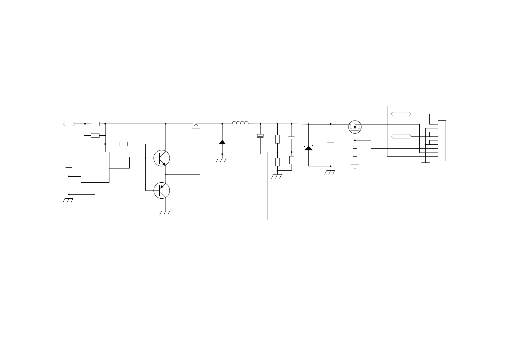
Power Board -- Circuit Diagram 2
+9-16Vdc
C16
471p
F/50V
B
2* 0.3R/12 06
67
3
MC34063
45
R32
R33
IC4
2
Q7
AF9435P
PI N1 ,2 ,3
R34
1K/0805
8
Q6
C945 SOT -23
PI N5 ,6 ,7 ,8
S
PI N4
G
D
D12
SB560
1
Q5
A733 SOT-23
L4
TO-6026
80uH/0.7mm
CE9
1000uF/10V
R37
9.1K/0805
R36
3K/0805
C15
N/O
R35
N/C
ZD3
6.2V /0.5 W
C24
Q4
APM4800 SOP-8
104/25V/1206
R38
10K/0805
STB
+20V/4A
9P/2.5
1
2
3
4
5
6
7
8
9
CON2
STB
GND
+17.5V
+17.5V
GND
GND
+12V/0.5A
D+5V/1.5A
MCU5V
12-7 12-7

Power Board -- Layout Diagram
T5AH 250V
12-8 12-8

Decoder Board -- Circuit Diagram 1
COMMON1389G_HD65_AT5669_V1.1
MT1389G (LQFP128) DVD Board w/ Sanyo HD6x Series PUHs
1 INDEX & POWER / RESET
2 MT1389G LQFP128
3 SDRAM & FLASH & MOTOR
4 AUDIO & MIC I/F
5 VIDEO I/F
6 MCR & USB I/F
TRIN
SSDA
SSCL
A_MUTE
MCU_HPD
CEC_INPUT
VIDEO_SW
CEC_OUT
3.3V_MCU
MCU_5V
CON2.0-5
CON2.0-5
J9
TRIN 2
SSDA 2
SSCL 2
A_MUTE 2
MCU_HPD 2
CEC_INPUT 2
VIDEO_SW 2
CEC_OUT 2
3.3V_MCU 2
MCU_5V 2
CLOSE_SW
1
GND
2
OPEN_SW
3
4
5
DV33
MCU RESET
+
CE3
+
0805-10UF-Z-0.1W-10V/NC
10K/NC
R8
D1
1N4148/NC
1 2
MCU_5V
R295
CE72
+
+
CD11X/220UF16V/D6.3H7
L34 FB
L35 FB
L36 FB
L37 FB
M+
10/1206
M-
R9
10K/NC
R298
R299
MM+
2
8550,DIP
8550,DIP
100
10K
6x2.0 W/HOUSING
R6
4.7K
DVD_RST
Q3
2N3904/NC
1 3
Q31
1 3
Q33
1 3
CN6
FPC16P
2
R290
2
R294
3.3V_MCU
1
2
3
4
5
6
7
8
9
10
11
12
13
14
15
16
10K
R7
470
470
R300
4.7k
OPEN/CL_SW
C121
0.01uF
TP28
URST#
3.3V_MCU
CEC_INPUT
CEC_OUT
SSDA
SSCL
A_MUTE
DVD_ON
DVD_RST
GND
VIDEO_SW
M_CLOSE
M_OPEN
OPEN/CL_SW
TP29
TP30
TP31
C2
ESD
8050,DIP
8050,DIP
MCU_HPD
GND
TP39
TP38
Q32
Q34
TP41
TP47
TP40
1 3
1 3
TP48
2
2
R297
TRIN
TP49
TP50
CON2.54-3
R292
10K
10K
etaDyrotsiH
Rev
5V
⬉⌕
standby40-60mA
Play
ᓔᴎ
570mA,
〇ᅮ⬉⌕
〇ᅮ⬉⌕
290-300mA,
130-140mA,
R3
2.2K
2
2.2uF/16V
L1 0R
1
220uF/16v
L2 FB/0603
47uF/6.3v
220uF/16v
2
CE2
730mA
〇ᅮ⬉⌕
〇ᅮ⬉⌕
C1
+
+
12
CE4
+
+
CE7
800mA
〇ᅮ⬉⌕
220uF/16v
+
+
R2
33K
360mA
340mA
A5VDC5V
CE5
᳔гᰃ
162.8mA
R4 1K
R5
22K
CB1
0.1uF
CB2
0.1uF
DV33
+
+
᳔гᰃ
AVCC
.
.
᳔гᰃ
VCC
+
+
CE1
CD11X/220UF16V/D6.3H7
DVD_ON
AVCC
RFV33
RFV33
TP1
TP1
89G_3V3
CB3
0.1uF
V12
CB4
0.1uF
V12
DVD5V
ⶀ䯈
1-1.25A
Play
CD5V
ᓔᴎ
570mA,
ⶀ䯈
1-1.25A
3.3V
⬉⌕
standby20-23mA
Play
ᓔᴎ
DVD3.3V
Play
CD3.3V
ᓔᴎ
290-300mA,
1.2V
⬉⌕
standby20-23mA
Play
ᓔᴎ
DVD&CD1.2V
12V
⬉⌕
standby2-3mA
Q1
CES2307
R1
47K
Q2
3904
1 3
TP51
TP52
TP53
TP54
P8
MCU_5V
1
DC5V
2
GND
3
2.0-3
R291
1K
C119
470pF
M_OPEN
R220
1K
M_CLOSE
C120
470pF
VCC
89G_3V3
V33_MD
V12_MD
V1
Original release
V1.1 2009.02.17
1),Modify CE31 from 47uF to 220uF for power noise improve;
2),Add 100 ohm resistance R160 and R161 to XI and XO nets for tune DPD performance;
3),Delete Q11 for costdown;
4),change L8 from 100uH to FB/200ohm.
MT1389G 128 PIN GPIO LIST
NAME PIN FEATURES
TRAY_OPEN
TRAY_CLOSE
FG / GPIO2
UP1_6
UP1_7
.
GPIO3
GPIO4
GPO5 7
GPIO6
GPIO7
GPIO8
GPIO9
14
VR_CD
VR_DVD
15
18
TRIN
28
29
HDMI_SCL
HDMI_SDA
34
35
TRCLOSE
31
39
SD_CLK
SD_CMD
SD_DATA
MS_CLK
MS_BS
MS_DATA
38
37
[STBY]
[TROPEN; IOA]
GPIO10 81 HPLG
GPIO11
GPIO12
GPIO13
GPO14 96
GPIO19
GPIO20
GPIO21
ARF
ARS
ALS
ALF
GPIO34
GPIO35
RFIN / OPOUT
MCU_5V
30
80
36
103
104
105
109
110
114
115
107
108
120
SCART1
ASPDIF
VSTB
A_MUTE
SCART2
AVCM
AKIN1
AUDIO_ARF
AUDIO_ARS
AUDIO_ALS
AUDIO_ALF
TROPEN IOA
STBY
LIMIT TROUT
C187
0.1uF/nc
U9 CX1117-3.3/NC
3
IN
1
ADJ
SOT223
OUT1
OUT2
HSYNC#
VSYNC#
2
4
47uF/16V/NC
RxD
3.3V_MCU
CE30
[Gxyz_D1#]
[Gxyz_D2#]
+
+
R301
10K
P#
2008.09.25
OFF-PAGE CONNECTION
URST#
URST# 2
AVCC
AVCC 2,3,4
DV33
DV33 2,3
V12_MD
V12_MD 3
V33_MD
V33_MD 2,3
RFV33
RFV33 2,4
89G_3V3
89G_3V3 2,3
V12
MARK2
U1
U1
PBZ-DVD
9
8
7
6
9
8
7
6
MARK3
V12 2
3
2
1
HOLE/GND
H4
2
2
9
3
3
8
4
4
7
5
5
6
1
1
HOLE/GND
H2
2
2
9
3
3
8
4
4
7
5
6
5
1
1
MARK4
Power
MARK1
12-9 12-9

Decoder Board -- Circuit Diagram 2
SANYO
HD6x/sony
HEADER 24 SMD0.5 TOP
1
2
3
4
5
6
7
8
9
10
11
12
13
14
15
16
17
18
19
20
21
22
23
24
CN3
V33_MD
RFV33
SP-
SP-A
V33_MD
FF+
T+
TC/c
D/d
CD/DVD SW
RF
A/a
B/b
F
GND-PD
Vc(Vref)
Vcc
E
NC
VR-CD
VR-DVD
CD-LD
MD
HFM
NC
DVD-LD
GND-LD
25
TOP
TOP
26
CB20
0.1uF
SLSL+
24
23
22
21
20
19
18
17
16
15
14
13
12
11
10
9
8
7
6
5
4
3
2
1
CE16
47uF/6.3v
R15 10k
R16
1R 0805
R18 10k
C42
0.1uF
10K
R20
TP7
V33_MD 1,3
RFV33 1,4
C17
NC
LD-DVD
2
MDI1
R37 0R
LD-CD
E
AVCC1
V20
CB17 0.1uF
F
B
A
RFO
IOA
D
C
T-
T+
F+
F-
V20
12
+
+
RF Reference
CB22
CB21
0.1uF
0.1uF
SP-A
VR_DVD
CB19
0.1uF
CB23
0.1uF
VR_CD
V12
V12
RFV12-1
L5 FB
V12
RFV12-2
L10 FB
Importance. layout close to IC pin.
C4
4.7uF/10v 0603
CB5 0.1uF
C7
4.7uF/10v 0603
CB9 0.1uF
89G_3V3
L9
FB
4.7uF/10V 0603
ADACVDD
RFVDD3
C10
DACVDD3DACVDD3
C8
0.1uF
CB7
0.1uF
0.1uF
SERVO RF DeCAP.
SERVO option 1# :
[No Gxyz, remove VR circuit]
TROPEN IOAGPIO34
STBYGPIO35
R27 100R27 100
PIN14
PIN15
AVCC
L12
FB/0603
CE14
+
+
47uF/16v
1 2
12
+
+
CE15
47uF/16v
0.1uF
LDO2
RFV33
LDO1
R29 100R29 100
89G_3V3
89G_3V3
USB-4P-90
V12
P1
0.1uF/10V
CB404
1
2
3
4
VR_CD
VR_DVD
R34 15k/NC
L13 FB/0603
4.7uF/10V 0603
L15 FB/0603
R36 5.1k 1%
L16 FB/0603
4.7uF/6.3V
TP33
TP32
TP37
VCC
SANYO 0
SANYO 100
RFV12-2
1
AVDD12_2
RFVDD3
2
R31 56
XI
XO
R30 56
CB13
C19
0.1uF
C20
4.7uF/6.3V
C21
UP1_6
R471 0
UP1_7
R472 0
TP34
R47 0
R48 0
USB_VCC2
C26
C41
C27
100pF
ESD
ESD
USB_EN0#
R426
10K
3
4
V20
5
V1P4
6
GPO5
7
MDI1
8
LDO1
9
LDO2
10
AVDD33
11
DMO
12
FMO
13
PIN14
14
PIN15
15
TRO
16
FOO
17
TRIN
18
USB_DP
19
USB_DM
20
USB_V33
21
22
USB_V12
23
SF_CS
24
SF_DO
25
SF_DI
26
SF_CK
27
28
29
RXD
30
GPIO6
31
URST#
32
TP46
89G_3V3
USB_DP
USB_DM
SMD0805P100TF 1A 6V/NC
L19
U410
1
IN
2
GND
EN#3FAULT#
TPS2552DBVT
AVDD33_1
XTALI
XTALO
V20
V14
REXT / GPO5
MDI1
LDO1
LDO2
AVDD33_2
DMO
FMO
TRAY_OPEN
TRAY_CLOSE
TRO
FOO
FG / GPIO2
USB_DP
USB_DM
VDD33_USB
PAD_VRT / GPIO37
VDD12_USB
SF_CS_
SF_DO
SF_DI
SF_CK
UP1_6 / SCL
UP1_7 / SDA
GPIO11
GPIO6
PRST#
OUT
ILIM
USB_VCC2
USB_OC0#
C
B
ADF
E
OPO
OP-
GPI36
129
121
120
122
127
124
123
126
125
128
RFF
RFE
RFB
RFA
RFD
RFC
E-PAD/GND
RFG / OPINP
RFH / OPINN
LQFP128/SMD/1389L
GPIO3 / INT#
IR
RD041RD142RD243RD344RD445RD546RD647RD748DQM049RD1550RD1451DVDD1252RD1353RD1254RD1155RD1056RD957RD858DQM159RCLK60RA1161RA962RA8
GPIO4
GPIO1336GPIO937DVDD33
GPIO838GPIO7 / CKE
35
39
34
33
40
DQ0
DQ1
USB_EN0#
USB_OC0#
GPIO3
GPIO4
10K
R428
89G_3V3
SSCL
R475 330
SSDA
R476 330
89G_3V3
R427 10K
6
5
4
R470
CB403
20K
CE401
0.1uF/10V
100uF/10V
C6
0.1uF
TP6
10uH
V1P4
+
+
CE17
47uF/6.3v
CB24
0.1uF
OP-
1
89G_3V3
D2
3
BAT54C
2
OPO
TP4
CN2
6x2.0 W/HOUSING
6
5
R21 0R
2
1
4
3
2
1
12
C18
+
CE12
+
0.1uF
100uF/10v
L18
L17
10uH
Q7
SOT23/D
2
SS8550
1 3
R40 4.7
R41 4.7
13
Q8
2
SOT23/D
SS8550
CB26
CB27
CB25
0.1uF
0.1uF
C5
0.1uF
TP5
SP+
LIMIT
TP8
1
12
V1289G_3V3
L6 FB/200
L7 FB
+
+
CB8
CE8
100uF/6.3v
+
+
C13 0.1uF
RFO
C16 1uFC16 1uF
ADACVDD
RFV12-1
DATA0
115
118
119
117
116
RFIP
AVDD12
ADACVDD2
ADACVDD1
CENTER / GPIO
RFIN / OPOUT / GPI36
MT1389G
DQ4
DQ5
DQ6
DQ2
DQ3
R473
4.7K
GPIO3
GPIO4
USB_VCC2
+
+
CE10 470uF/6.3v
LRCK
114
ALS / GPIO
U2
DQ7
89G_3V3
R401
510
R0603B
89G_3V3
FB/100uH
L8
AADVDD
12
+
+
C9
CE9
6800pF
220uF/6.3v
CON1
CON2.0-4
10uF/10v 0805
TP45
C15
R28
V_G
V_B
V_R
GPIO35
GPIO34
BCK
MCLK
AADVDD
107
111
110
113
109
105
108
112
106
AVCM
AADVDD
AL / GPIO
AR / GPIO
LFE / GPIO
ARS / GPIO
AKIN1 / GPIO21
PAD_APLLCAP / GPIO35
APLLVDD_GPIO / GPIO34
DQM0
DQ15
DQ14
DQ13
DQ12
DQ11
DQ10
DQ9
V12
R474
4.7K
560
GPIO20
DACVDD3
CVBS_OUT
104
103
101
100
97
102
98
99
B
R
G
FS
CVBS
DACVDDB
VREF / GPO14
AKIN2 / GPIO19
DACVDDC
ADVCM / GPIO20
TX2P
TX2N
AVDD12_D
TX1P
TX1N
AVSS12
TX0P
TX0N
AVDD12_C
TXCP
TXCN
AVDD33_12
EXT_RES
GPIO10 / HPLG
SPDIF / GPIO12
DVDD12
RA3
RA2
RA1
RA0
RA10
BA1
BA0
DVDD33
RAS#
CAS#
RWE#
RA4
RA5
RA6
RA7
63
64
DQ8
DQM1
DCLK
MA11
MA9
MA8
MA7
R46
5
2 1
R22
4
2 1
R23
3
2 1
R24
2
2 1
1
TP17
TP15
TP13
TP14
TP12
DACVDD3
21
R32 4.7k
R33 330
GPO14
96
DACVDD3
95
TX2+
94
TX2-
93
92
TX1+
91
TX1-
90
89
TX0+
88
TX0-
87
86
TXC+
85
TXC-
84
83
R35 2.5K 1%
82
89G_HPD
81
ASPDIF
80
79
78
77
76
75
74
73
72
71
70
69
68
67
66
65
FOSO
TRSO
FMSO
DMSO
V12
MA3
MA2
MA1
MA0
MA10
BA1
BA0
89G_3V3
RAS#
CAS#
WE#
MA4
MA5
MA6
C23
C23
330pF
330pF
RS-232
GPIO11 need to pull-up.
89G_3V3
C43
C43
C44
C44
330pF
330pF
330pF
330pF
R50
R50
4.7k
4.7k
RXD
R19 FB/0603
2 1
22
22
22
22
C24
C24
330pF
330pF
TP36TP36
RXD
XIXIXI
C11
27pF
Put these circuits as
closer as possible to
MT1389
C46
C3
100p
100p
A_MUTE
CB12
0.1uF
CB14
0.1uF
C22
C22
0.1uF
0.1uF
DV33
TP35TP35
RxD
TxD
4x2.0 W/HOUSING
4x2.0 W/HOUSING
1#1#
Crystal
R17 100k
27MHz+_10PPM
L39 FB/1K
L40 FB1K
L41 FB/1K
L42 FB/1K
C14
C45
100p
100p
SSDA
SSCL
89G_HPD
A_MUTE
CE11
4.7uF/10V 0603
21
CE13
4.7uF/10V 0603
R42 27kR42 27k
R43 27kR43 27k
R44 15kR44 15k
R45 10kR45 10k
C25
C25
0.015uF
0.015uF
CN4
CN4
1
2
3
4
tluafeDtluafeD
Y1
MCLK
BCK
LRCK
DATA0
L11 FB/0603
MOSFET N CES2312
L14 FB
V1P4
C12
27pF
SSDA 2
SSCL 2
89G_HPD 2
A_MUTE
Q6
FOO
TRO
FMO
DMO
OFF-PAGE CONNECTION
XOXO
XO
DRAM I/F
S-FLASH
IIC I/F
VIDEO I/F
V12
AUDIO I/F
13
89G_3V3
SOT23/D
2
USB I/F
AVCC
SERVO I/F
TMDS I/F
Power
TXDGPIO6
DQ[0..15]
MA[0..11]
DQM[0..1]
BA[0..1]
DCLK
RAS#
CAS#
WE#
SF_CK
SF_CS
SF_DI
SF_DO
UP1_[6..7]
CVBS_OUT
V_R
V_B
V_G
ASPDIF
STBY
TRIN
TT+
FF+
SLSL+
SP-
SP+
FOSO
TRSO
FMSO
DMSO
V1P4
TXC+
TXC-
TX0+
TX0-
TX1+
TX1-
TX2+
TX2-
HPLG
UP1_[6..7]
URST#
AVCC
DV33
89G_3V3
V12
RFV33
SF_CK 3
SF_CS 3
SF_DI 3
SF_DO 3
CVBS_OUT 4
V_R 4
V_B 4
V_G 4
ASPDIF 5
STBY 3
TRIN 3
T- 3
T+ 3
F- 3
F+ 3
SL- 3
SL+ 3
SP- 3
SP+ 3
FOSO 3
TRSO 3
FMSO 3
DMSO 3
V1P4 3
TXC+ 4
TXC- 4
TX0+ 4
TX0- 4
TX1+ 4
TX1- 4
TX2+ 4
TX2- 4
HPLG 4
LIMIT TROUTGPI36
URST# 1
AVCC 1,3,4
DV33 1,3
89G_3V3 1,3
V12 1
RFV33 1,4
DQ[0..15] 3
MA[0..11] 3
DQM[0..1] 3
BA[0..1] 3
DCLK 3
RAS# 3
CAS# 3
WE# 3
UP1_[6..7] 4
UP1_[6..7] 4
TRCLOSEGPO5
12-10 12-10

Decoder Board -- Circuit Diagram 3
MD_VCC
CB34
0.1uF
ESMT M12L64164A
U3
SR_3V3
DCLK
BA0
BA1
RAS#
CAS#
WE#
R54 10k
R55 10k
C28 15pF/NC
R56 200
R58 0
R59 0
1 2
1 2
1 2
R61 0R
R60 0R
R62 0R
89G_3V3
SDCKE MA8
DCS#
SDCLK
R57 33/FB
SF_CS
SF_DO
R64 10k
SDCLK
DBA0
DBA1
DRAS#
DCAS#
DWE#
MA0
MA1
MA2
MA3
MA4
MA5
MA6
MA7
MA9
MA10
MA11
DBA0
DBA1
SDCLK
SDCKE
DCS#
DRAS#
DCAS#
DWE#
DQM0
DQM1
EN25F16
U4
1
CE#
2
SO
3
WP#
VSS4SI
2MB
R65 10k
23
24
25
26
29
30
31
32
33
34
22
35
20
21
38
37
19
18
17
16
15
39
36
40
54
41
28
HOLD#
VDD
SCK
A0
A1
A2
A3
A4
A5
A6
A7
A8
A9
A10/AP
A11
BA0/A13
BA1/A12
CLK
CKE
CS
RAS
CAS
WE
DQML
DQMH
NC
NC
VSS
VSS
VSS
8
7
6
5
HOLD#
SF_CK
SF_DI
SF_CS
DQ0
DQ1
DQ2
DQ3
DQ4
DQ5
DQ6
DQ7
DQ8
DQ9
DQ10
DQ11
DQ12
DQ13
DQ14
DQ15
VCC
VCC
VCC
VCCQ
VCCQ
VCCQ
VCCQ
VSSQ
VSSQ
VSSQ
VSSQ
89G_3V3
C29
0.1uF
2
4
5
7
8
10
11
13
42
44
45
47
48
50
51
53
1
14
27
3
9
43
49
6
12
46
52
R63 10k
DQ0
DQ1
DQ2
DQ3
DQ4
DQ5
DQ6
DQ7
DQ8
DQ9
DQ10
DQ11
DQ12
DQ13
DQ14
DQ15
SR_3V3
SR_3V3
SerialFlash
T-
15
CB38
0.1uF
VOTK+
16
VOTK-
17
VOLD+
18
VOLD-
19
VCC2
20
NC
21
VCTL
30
G2
22
GND
23
VINLD
24
NC
25
TRB2
26
VINTK
27
BIAS
28
MUTE
U5
5888S
HSOP28/SMD
T+
SL+
SL-
FMSO
ADJ_12
TRSO
V1P4
STBY
R77
10k
VOFC+
VOFC-
VOSLVOSL+
VOTR+
VOTR-
FWD
REGO1
VINSL+
REGO2
TRB1
VINFC
VCC
REV
F+
14
F-
13
SP-
12
SP+
11
10
9
8
29
G1
7
6
5
R72 10k
4
3
ADJ_33
2
FOSO
1
CB35
0.1uF
DMSO
MD_VCC
12
L22 FB
CE21
+
+
220uF/16v
1
1
AVCC
10R
R73
FBI_33
10R
R76
FBI_12
ADJ_12
FBI_12
2
Q11
SS8550D
89G_3V3
L20 FB
CE19
+
+
100uF/6.3v
SR_3V3
CB31
0.1uF
CB32
0.1uF
CB30
0.1uF
VCC DeCap VCCQ DeCap
SDR_DRAM (Dual Layout)
89G_3V3
CD190mA
DVD196mA
D12 IN4004/SMD
13
R68
1K
TO-92A
1.2V output
2
TP42
1
V12_MD
RaRb0NC20K
CB36
0.1uF
2
D13
IN4004/SMD
ADJ_33
FBI_33
AM5888AT5669
12K
1
2
Ra
V3.3/ferV
Rb
SR_3V3
CB29
0.1uF
CB33
0.1uF
DVD377mA
CD358mA
IN4004/SMD
D14
2
13
Q12
SS8550D
TO-92A
R69
15k
R75
9.1k
L21 FB
1
CE20
+
+
100uF/10v
V33_MD
TP43
CB37
0.1uF
AVCC
W2W2
1
2
OFF-PAGE CONNECTION
DQ[0..15]
MA[0..11]
DQM[0..1]
BA[0..1]
DCLK
RAS#
CAS#
WE#
DRAM I/F
SF_CK
SF_CS
SF_DI
SF_DO
S-FLASH
STBY
TT+
FF+
SLSL+
SPSP+
FOSO
TRSO
FMSO
DMSO
V1P4
SERVO I/F
DV33
V12_MD
V33_MD
Power
URST#
Misc
AVCC
89G_3V3
DQ[0..15] 2
MA[0..11] 2
DQM[0..1] 2
BA[0..1] 2
DCLK 2
RAS# 2
CAS# 2
WE# 2
SF_CK 2
SF_CS 2
SF_DI 2
SF_DO 2
STBY 2
T- 2
T+ 2
F- 2
F+ 2
SL- 2
SL+ 2
SP- 2
SP+ 2
FOSO 2
TRSO 2
FMSO 2
DMSO 2
V1P4 2
DV33 1,2
V12_MD 1
V33_MD 1,2
URST# 1,2
AVCC 1,2,4
89G_3V3 1,2
12-11 12-11

Decoder Board -- Circuit Diagram 4
V_G
R85
75/NC
75/NC
V_R
R106
75/NC
CON2
CON2.0-4/NC
4
3
2
1
CVBS_OUT
75/NC
R89
R81
SC_IPOD
SY_IPOD
VIDEO_IPOD
L23 1.8uH/SMD/NC
C32
47pF/NC
L24 1.8uH/SMD/NC
C34
47pF/NC
L26 1.8uH/SMD/NC
C36
47pF/NC
L27
C38
47pF/NC
VIDEO_DVD
VIDEO_SW
1.8uH/SMD/NC
G/Y/DVD
SC_IPOD
B/U/DVD
VIDEO_IPOD
R/V/DVD
SY_IPOD
VIDEO_IPOD
R121 33/NC
OFF-PAGE CONNECTION
CVBS_OUT
CVBS_OUT 2
V_R
V_R 2
V_B
V_B 2
V_G
V_G 2
G/Y_OUT
6
12
B/U_OUT
D4
ESD/NC
VIDEO_DVD
C33
47pF/NC
R133 0/NC
33/NC
2
3
5
6
11
10
14
13
1
15
R131 0/NC
R130 0/NC
R128 0/NC
R129 0/NC
PT2328/NC
SSOP16
S1A
S2A
S1B
S2B
S1C
S2C
S1D
S2D
IN
/EN
G/Y/DVD
B/U/DVDV_B
R/V/DVD
U6
L29 FB/0603
L30 FB/0603
L31 FB/0603
G/Y_OUT
B/U_OUT
R/V_OUT
L32 FB/0603
VIDEO_OUT
CB46
0.1uF
VCC
+
+
CE29
CD11X/47UF16V/D5H7/NC
4
DA
7
DB
9
DC
R132 0/NC
12
DD
16
VDD
8
GND
C35
47pF/NC
C37
47pF/NC
C39
47pF/NC
R123
4
12
R/V_OUT
2
D6
ESD/NC
12
D8
ESD/NC
AV3-8.4-14D/NC
AV3-8.4-14D
P2
HDMI_CLK
HDMI_SDA
UP1_6
UP1_7
CEC_INPUT
CEC_OUT
5
3
1
HDMI I/F
R109
1.8K
TX2+
TX2-
TX1+
TX1-
TX0+
TX0-
TXC+
TXC-
HDMI_VCC
1
D24
NC
3.3V_MCU
C31
330pF/NC
R418 0/NC
2
1
2
1
C30 0.1uF/NC
D16
NC
D17
NC
D19
NC
D25
NC
L38 FB/0603/NC
SPDIF
COAXIAL
VIDEO_OUT
COAXIAL
P6
GPIF32T/NC
5
4
3
2
1
GPIF32T
TXC+
TXC-
TX0+
TX0-
TX1+
TX1-
TX2+
TX2-
HPLG
UP1_[6..7]
TXC+ 2
TXC- 2
TX0+ 2
TX0- 2
TX1+ 2
TX1- 2
TX2+ 2
TX2- 2
HPLG 2
UP1_[6..7] 2
TMDS I/F
AVCC
AVCC 1,2,3
DV33
DV33 1,2,3
POWER
CEC_INPUT
CEC_INPUT 2
CEC_OUT
CEC_OUT 2
MCU_HPD
MCU_HPD 2
89G_HPD
89G_HPD 2
3.3V_MCU
3.3V_MCU 2
MCU_5V
MCU_5V 2
ASPDIF
ASPDIF 5
VIDEO_SW
VIDEO_SW 5
89G_3V3
89G_3V3 5
2221
1
2
3
4
5
6
7
8
9
10
11
R99 0
D21
NC
HDMI_VCC
12
CEC
13
ARC
14
15
16
17
18
HPLG
19
R1 0 4 0 R
J1
HDMI TYPE-A
20 23
D23
NC
+
+
CB44
CE28
0.1uF
100uF/16V
3.3V_MCU
2
89G_3V3
R112
4.7K
13
Q19
2N3906
R117 1K
MCU_HPD
R113
4.7K
89G_HPD
13
Q20
2
2N3906
CECOUT
TP44
UP1_6
UP1_7
D22
NC
MCU_5V
L28 FB
D26
NC
CEC
ARC
D27
D28
NC
NC
R116 1K
HPLG
R119
47K
R78 100/NC
ASPDIF
TMDS signal:
1),Via on signal is forbidden;
2),TMDS siganl length must less than 5cm;
3),Differential impedance must control at
100 ohm.
R111
1.8K
C40
10PF
R120 100K
R115
R118 47K
2
R114
18K
R79
100/NC
AVCC
R419 33/NC
CON5
AV1-8.4-14D(Black˅
AV1-8.4-8D
CON6
AV1-8.4-14D(Yellow)
AV1-8.4-8D
D15
NC
D18
NC
D20
NC
CEC3.3V
VDD_CEC
L33
FB/0603
27K
12
D11
SS14(5819)
CECOUT
Q21
2N3904
1 3
R122
220
CEC
12-12 12-12

Decoder Board -- Layout Diagram
12-13 12-13

Exploded View
Aluminual Top Cover
TC
CBP1 、CBP2
CBP3
Display Lens
DDR
ALU. Front Panel
VKP
UD
Filter Lens
FC
Spring
FBP
Dust cover
CDB
UBA
Screw
HBA
Screw
Bottom cover
PCB1
Back cover
Screw
PCB2
LM
Screw
Screw
PBP
Screw
Plastic Foot
Screw
Rubber Foot
13-1 13-1

Revision List
Version 1.0
* Initial Release
Revision List
14-1
 Loading...