

Page 1
Philips Semiconductors Linear Products Product specification
MC/SA1458/MC1558General purpose operational amplifier
59
August 31, 1994 853-1062 13721
DESCRIPTION
The MC1458 is a high-performance operational amplifier with high
open-loop gain, internal compensation, high common-mode range
and exceptional temperature stability. The MC1458 is short-circuit
protected.
The MC1458/SA1458/MC1558 consists of a pair of 741 operational
amplifiers on a single chip.
FEATURES
•Internal frequency compensation
•Short-circuit protection
•Excellent temperature stability
•High input voltage range
•No latch-up
•1558/1458 are 2 “op amps” in space of one 741 package
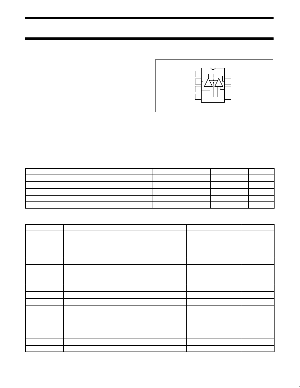
PIN CONFIGURATION
1
2
3
4 5
6
7
8
– +
+
–
A B
V+
OUTPUT B
INVERTING INPUT B
NON -INVERTING INPUT B
OUTPUT A
INVERTING INPUT A
NON -INVERTING INPUT A
V–
D, N Packages
TOP VIEW
ORDERING INFORMATION
DESCRIPTION TEMPERATURE RANGE ORDER CODE DWG #
8-Pin Plastic Small Outline (SO) Package 0 to +70°C MC1458D 0174C
8-Pin Plastic Dual In-Line Package (DIP) 0 to +70°C MC1458N 0404B
8-Pin Plastic Small Outline (SO) Package -40°C to +85°C SA1458D 0174C
8-Pin Plastic Dual In-Line Package (DIP) -40°C to +85°C SA1458N 0404B
8-Pin Plastic Dual In-Line Package (DIP) -55°C to +125°C MC1558N 0404B
ABSOLUTE MAXIMUM RATINGS
SYMBOL PARAMETER RATING UNIT
V
S
Supply voltage
MC1458 ±18 V
SA1458 ±18 V
MC1558 ±22 V
T
J
Junction temperature +150 °C
P
D MAX
Maximum power dissipation,
TA=25°C (still-air)
1
N package 1160 mW
D package 780 mW
V
DIFF
Differential input voltage ±30 V
V
IN
Input voltage
2
±15 V
Output short-circuit duration Continuous
T
A
Operating ambient temperature range
MC1458 0 to +70 °C
SA1458 -40 to +85 °C
MC1558 -55 to +125 °C
T
STG
Storage temperature range -65 to +150 °C
T
SOLD
Lead soldering temperature (10sec max) 300 °C
NOTES:
1. The following derating factors should be applied above 25°C; N package at 9.3mW/°C; D package at 6.2mW/°C
2. For supply voltages less than ±15V, the absolute maximum input voltage is equal to the supply voltage.
Page 2
Philips Semiconductors Linear Products Product specification
MC/SA1458/MC1558General purpose operational amplifier
August 31, 1994
60
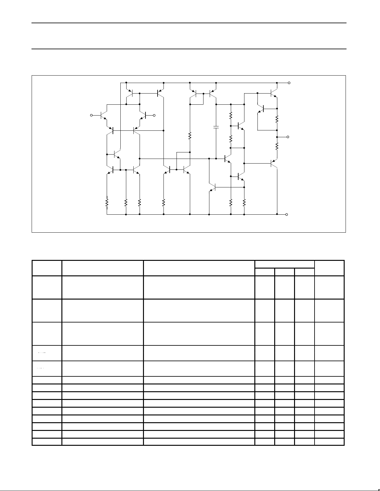
EQUIVALENT SCHEMATIC
Amplifier “A” of MC1458, SA1458, MC1558
NON–INVERTING
INPUT
3
Q1
Q8
Q2
Q3
Q4
Q7
Q5
Q6
R1
1KΩR250KΩ
R3
1kΩ
INVERT.
INPUT
Q9 Q12
Q13
R5
39KΩ
Q10
Q11
Q22
V+
Q14
R9
25Ω
1
OUTPUT
R10
50Ω
Q20
Q16
Q17
Q18
Q15
8
4
V–
R11
50Ω
R12
50kΩ
R7
4.5KΩ
R8
7.5KΩ
R4
5kΩ
2
DC ELECTRICAL CHARACTERISTICS
TA=25°C, VS=±15V, unless otherwise specified.
MC1558
SYMBOL
PARAMETER
TEST CONDITIONS
Min Typ Max
UNIT
V
OS
Offset voltage RS=10kΩ 1.0 5.0 mV
RS=10kΩ, over temperature 6.0 mV
∆V
OS
Offset voltage Over temperature 10 µV/°C
I
OS
Offset current 20 200 nA
Over temperature 500 nA
∆I
OS
Offset current Over temperature 0.10 nA/°C
I
BIAS
Input bias current 80 500 nA
Over temperature 1500 nA
∆I
BIAS
Bias current Over temperature 1.0 nA/°C
RL=10kΩ, over temperature ±12 ±14
V
OUT
Output voltage swing
RL=2kΩ, over temperature ±10 ±13
V
RL=2kΩ,VO=±10V 50 100
A
VOL
Large-signal voltage gain
RL=2kΩ, VO=± temperature 20
V/mV
Offset voltage adjustment range ±30 mV
PSRR Power supply rejection ratio RS≤10kΩ 30 150 µV/V
CMRR Common mode rejection ratio 70 90 dB
I
CC
Supply current 2.3 5.0 mA
V
IN
Input voltage range ±12 ±13 V
P
D
Power consumption 70 150 mW
Channel separation 120 dB
R
OUT
Output resistance 75 Ω
I
SC
Output short-circuit current 10 25 60 mA
Page 3
Philips Semiconductors Linear Products Product specification
MC/SA1458/MC1558General purpose operational amplifier
August 31, 1994
61
DC ELECTRICAL CHARACTERISTICS (Continued)
TA=25°C VCC=±15V, unless otherwise specified.
MC1458 SA1458
SYMBOL
PARAMETER
TEST CONDITIONS
Min Typ Max Min Typ Max
UNIT
V
OS
Offset voltage RS=10kΩ 2.0 6.0 2.0 6.0 mV
RS=10kΩ, over temp. 7.5 7.5 mV
∆V
OS
Offset voltage Over temperature 12 12 µV/°C
I
OS
Offset current 20 200 20 200 nA
Over temperature 300 500 nA
∆I
OS
Offset current Over temperature 0.10 0.10 nA/°C
I
BIAS
Input bias current 80 500 80 500 nA
Over temperature 800 1500 nA
∆I
BIAS
Bias current Over temperature 1.0 1.0 nA/°C
RL=10kΩ, over temp. ±12 ±14 ±12 ±14
V
OUT
Output voltage swing
RL=2kΩ, over temp. ±10 ±13 ±10 ±13
V
RL=2kΩ, VO=±10V 25 200 20 200 V/mV
A
VOL
Large-signal voltage gain RL=2kΩ, VO=±10V,
Over temperature 15 15 V/mV
Offset voltage adjustment range ±30 ±30 mV
PSRR Power supply rejection ratio RS≤10kΩ 30 150 30 150 µV/V
CMRR Common-mode rejection ratio 70 90 70 90 dB
I
CC
Supply current 2.3 5.6 2.3 5.6 mA
V
IN
Input voltage range ±12 ±13 ±12 ±13 V
R
IN
Input resistance 0.3 1 0.3 1 MΩ
P
D
Power consumption 70 170 70 170 mW
Channel separation 120 120 dB
I
SC
Output short-circuit current 25 25 mA
AC ELECTRICAL CHARACTERISTICS
TA=25°C VS=±15V, unless otherwise specified.
SYMBOL
PARAMETER
TEST CONDITIONS
MC1458, SA1458,
MC1558
UNIT
SYMBOL
PARAMETER
TEST CONDITIONS
Min Typ Max
UNIT
R
IN
Parallel input resistance Open-loop, f=20Hz 0.3 MΩ
Common-mode input impedance f=20Hz 200 MΩ
Equivalent input noise voltage AV=100, RS=10kΩ, BW=1.0kHz, f=1.0kHz 30
nV Hz
BW Power bandwidth AV=1, RL=2.0kΩ, THD≤5%, V
OUT
=20V
P-P
14 kHz
Phase margin 65 degrees
A
V
Gain margin 11 dB
Unity gain crossover frequency Open loop 1.0 MHz
Transient response unity gain VIN=20mV, RL=2kΩ, CL≤100pF
t
R
Rise time 0.3 µs
Overshoot 5.0 %
SR Slew rate CL≤100pF, RL≥2kΩ, VIN=±10V 0.8 V/µs
Page 4
Philips Semiconductors Linear Products Product specification
MC/SA1458/MC1558General purpose operational amplifier
August 31, 1994
62
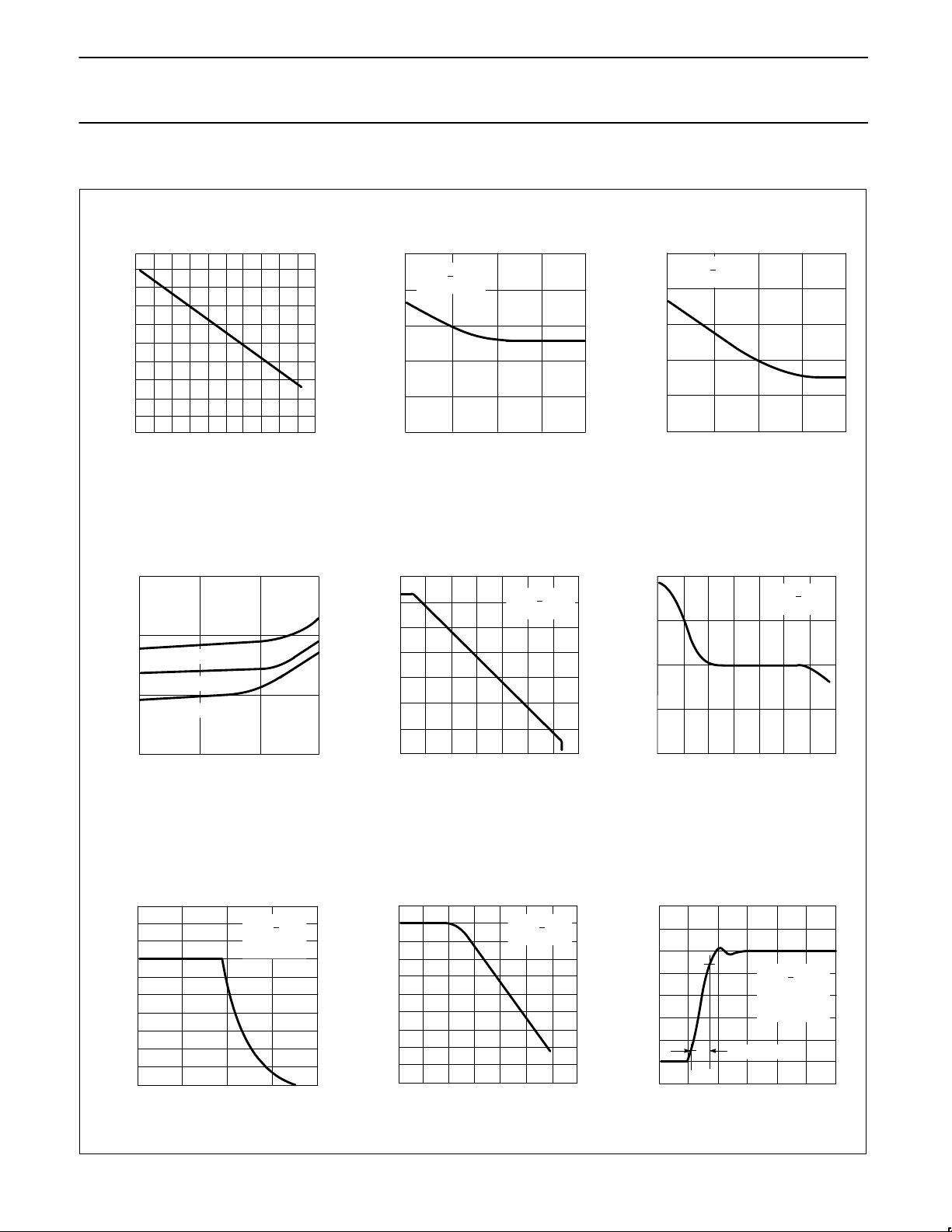
TYPICAL PERFORMANCE CHARACTERISTICS
VS = +15V
–55oC < TA < + 125OC
R
L
> 2kΩ
40
36
32
28
24
20
16
12
8
4
0
5 10 15 20
SUPPLY VOLTAGE — +
V
PEAK–TO–PEAK OUTPUT SWING — V
Output Voltage Swing as a
Function of Supply Voltage
–55oC < TA < + 125OC
16
14
12
10
8
6
4
2
0
5 10 15 20
SUPPLY VOLTAGE — +
V
COMMON MODE VOLTAGE RANGE – V
+
Input Common–Mode Range
as a Function of Supply Voltage
T
A
= 25
o
C
100
80
60
40
20
0
5 10 15 20
POWER CONSUMPTION — mW
SUPPLY VOLTAGE — +V
500
400
300
200
100
0
–60 –20 20 60 100 140
TEMPERATURE — oC
INPUT BIAS CURRENT — nA
VS = +15V
10.0
5.0
3.0
1.0
0.5
0.3
INPUT RESISTANCE — MΩ
0.1
–60 –20 20 60 100 140
TEMPERATURE — oC
T
A
= 25oC
40
30
20
10
0
5
10 15
20
INPUT OFFSET CURRENT — nA
SUPPLY VOLTAGE — +V
Input Bias Current as a
Function Of Ambient Temperature
Input Resistance as a
Function of Ambient Temperature
Power Consumption as a
Function of Supply Voltage
Input Offset Current as a
Function of Supply Voltage
VS = +15V
140
120
100
80
60
40
20
0
–60 –20 20 60 100 140
TEMPERATURE —
o
C
INPUT OFFSET CURRENT — nA
TEMPERATURE — oC
POWER CONSUMPTION — mV
70
60
50
40
30
–60 –20 20 60 100 140
Input Offset Current as a
Function of Ambient Temperature
Power Consumption as a
Function of Ambient Temperature
28
26
24
22
20
18
16
14
12
10
8
0.1 0.2 0.5 10 2.0 5.0 1.0
LOAD RESISTANCE — kΩ
PEAK–TO–PEAK OUTPUT SWING — V
VS = + 15V
T
A
= 25oC
Output Voltage Swing as a
Function of Load Resistance
Page 5
Philips Semiconductors Linear Products Product specification
MC/SA1458/MC1558General purpose operational amplifier
August 31, 1994
63
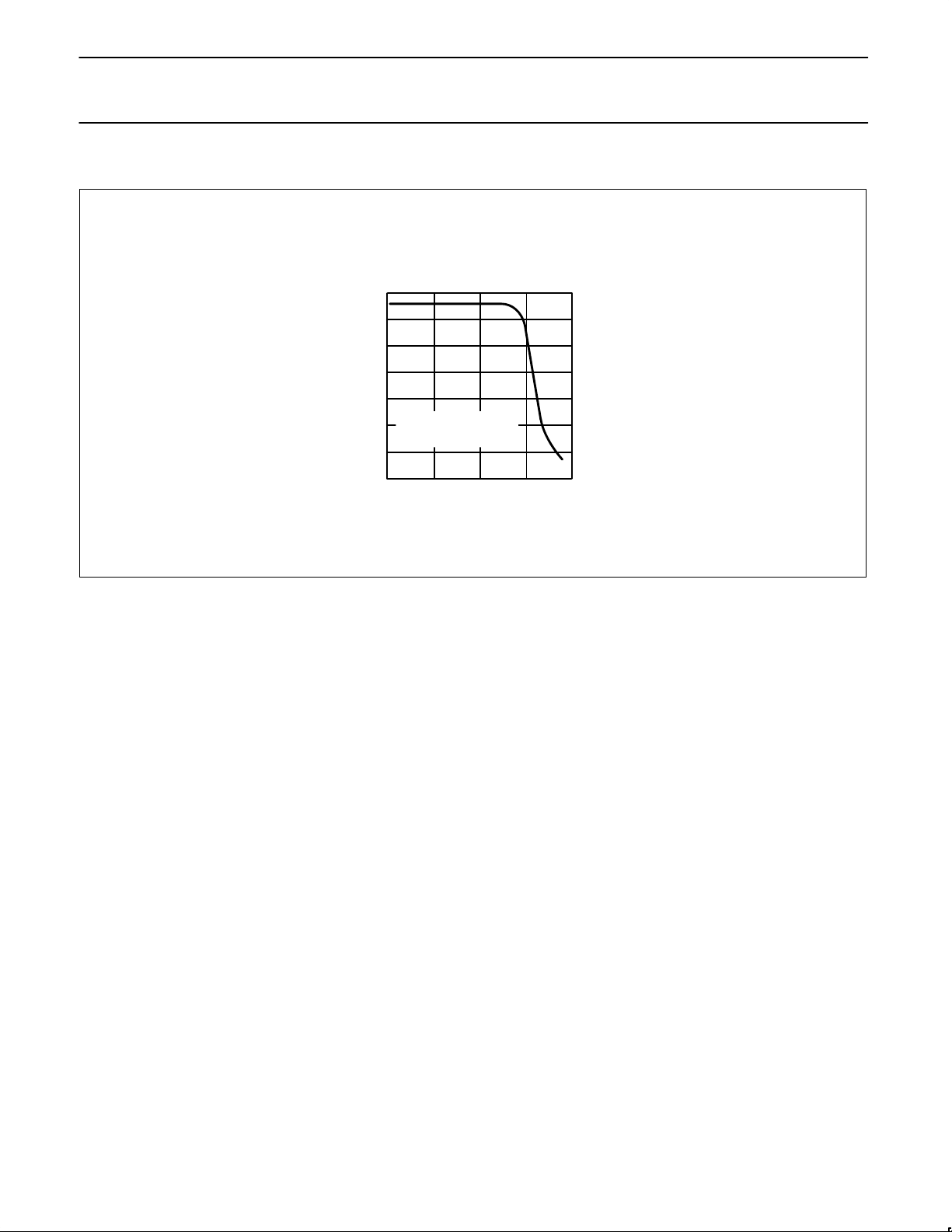
TYPICAL PERFORMANCE CHARACTERISTICS (Continued)
MEAN SQUARE VOLTAGE — A Hz
2
10–1kHz
35
30
25
20
15
10
–60 –20 20 60 100 140
TEMPERATURE —
o
C
SHORT CIRCUIT CURRENT — mA
VS = + 15V
T
A
= 25oC
10
–13
10
–14
10
–15
10
–16
10
–17
10
–18
10 100 1K 10K 100K
FREQUENCY — Hz
MEAN SQUARE VOLTAGE — V Hz
2
VS = + 15V
T
A
= 25oC
MEAN SQUARE CURRENT
10
–21
10
–22
10
–23
10
–24
10
–25
10
–26
10 100 1K 10K 100K
FREQUENCY — Hz
100
10
1
0.1
100 1K 10K 100K
10–100kHz
10–100kHz
SOURCE RESISTANCE — Ω
TOTAL NOISE REFERRED TO INPUT — Vrmsµ
VS = + 15V
T
A
= 25oC
10
6
10
5
10
4
10
3
10
2
10
1
1 10 100 1K 10K 100K 1M 10M
FREQUENCY — Hz
VOLTAGE GAIN
1 10 100 1K 10K 100K 1M 10M
FREQUENCY — Hz
VS = + 15V
T
A
= 25oC
0
–45
–90
–135
–180
PHASE DEGREES
VS = + 15V
T
A
= 25oC
R
L
= 10kΩ
40
36
32
28
24
20
16
12
8
4
0
100 1K 10K 100K 1M
FREQUENCY — Hz
PEAK–TO–PEAK OUTPUT SWING — V
VS = + 15V
T
A
= 25oC
100
90
80
70
60
50
40
30
20
10
1 10 100 1K 10K 100K 1M 10M
FREQUENCY — Hz
COMMON MODE REJECTION RATE — dB
28
24
20
16
12
8
4
0
OUTPUT — mV
0 0.5 1.0 1.5 2.0 2.5
TIME — µs
VS = + 15V
T
A
= 25oC
R
L
= 2kΩ
C
L
= 100pF
RISE TIME
Output Short–Circuit Current as a
Function of Ambient Temperature
Input Noise Voltage as a
Function of Frequency
Input Noise Current as a
Function of Frequency
Broadband Noise for
Various Bandwidths
Open–Looped Voltage Gain
as a Function of Frequency
Open-Looped Phase Response
as a Function of Frequency
Output Voltage Swing
as a Function of Frequency
Common–Mode Rejection Ratio
as a Function of Frequency
Transient Response
Page 6
Philips Semiconductors Linear Products Product specification
MC/SA1458/MC1558General purpose operational amplifier
August 31, 1994
64
TYPICAL PERFORMANCE CHARACTERISTICS (Continued)
28
24
20
16
12
8
4
0
10 100 1K 10K 100K
(VOLTAGE FOLLOWER)
+ 15 VOLT SUPPLIES
THD < 5%
V OUTPUT VOLTAGE (Vp–p)
OUT
FREQUENCY — Hz
Power Bandwidth
(Large–Signal Swing vs Frequency)
 Loading...