

Page 1

Service Manual
Service
Service
DVD Receiver
Service
Service
Service
LX8500W/01/04/69/93
©
Copyright 2004 Philips Consumer Electronics B.V. Eindhoven, The Netherlands
All rights reserved. No part of this publication may be reproduced, stored in a retrieval system or
transmitted, in any form or by any means, electronic, mechanical, photocopying, or otherwise
without the prior permission of Philips.
Published by BB0435 Service AV Systems Printed in The Netherlands Subject to modification
Version 1.0
TABLE OF CONTENTS
Page
Location of pc boards & Version variations................1-2
Technical Specifications ............................................. 1-3
Measurement setup ....................................................1-4
Service Aids, Safety Instruction, etc. .........................1-5
Disassembly Instructions & Service positions .............. 2
Service Test Program .................................................3-1
Region code, Software version & upgrades...............3-2
Set Block diagram ......................................................4-1
Set Wiring diagram .....................................................5-1
Panel Front Boards........................................................ 6
AV Board........................................................................ 7
Box Spk Assy SW8500LX ............................................. 8
Module SD6.3 ST AV2 ...................................................9
Set Mechanical Exploded view & parts list ................. 10
Speaker Box Exploded view & parts list .................. 11-1
Speaker Box Disassembly Instructions .................... 11-2
CLASS 1
LASER PRODUCT
GB
3139 785 30820
Page 2
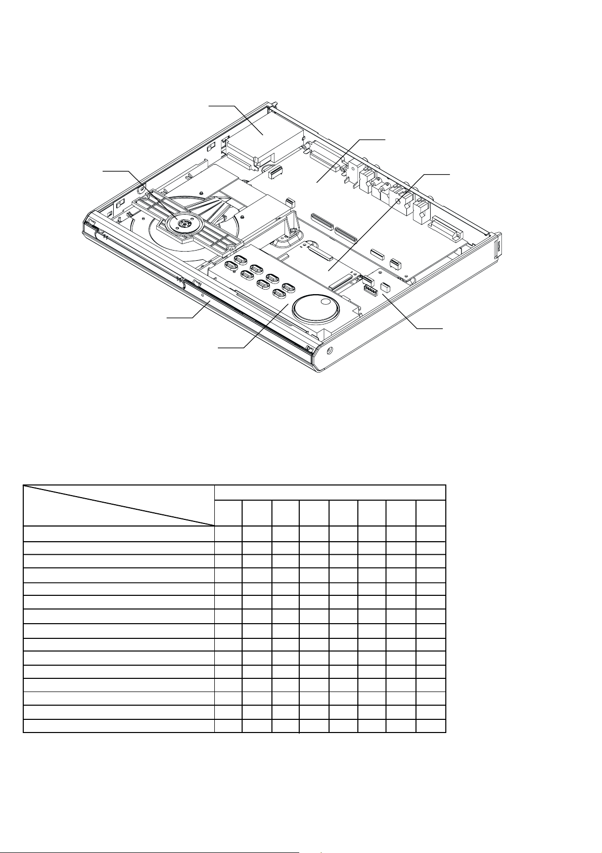
LOCATION OF PC BOARDS
Tuner Module
1-2
AV Board
DVD Loader
Front IR/FTD/LED Board
Front Key Board
SD6.3 Board
Front Board
VERSION VARIATIONS:
Type /Versions: LX8500W
Features &
Board in used:
Progressive Scan xxxx
Voltage Selector x x
Digital In xxxx
TV-In x x
Aux-In xxxx
Line-Out xxxx
Video Output xxxx
S-Video Output xxxx
SCART x x
Y/Pb/Pr (YUV) Component Video Output xxxx
/01 /04 /69 /93
Page 3

SPECIFICATIONS
GENERAL:
Mains voltage : 120V for /17
220-240V for /01/04
110-127V/220-240V Switchable for /69/93
Mains frequency : 50/60Hz
Power consumption : < 1W at Standby
< 130W at 1/8 P
< 35W at 1/8 P
(For main & subwoofer unit)
rated
(For surround unit)
rated
Dimension main unit : 360 x 40 x 305mm
TUNER:
FM
Tuning range : 87.5-108MHz
Grid : 50kHz
100kHz for /17/69
IF frequency : 10.7MHz ± 25kHz
Aerial input : 75Ω coaxial
Sensitivity at 26dB S/N : < 7µV
Selectivity at 600kHz bandwidth : > 25dB
IF rejection : > 60dB
Image rejection : > 25dB
Distortion at RF=1mV, dev. 75kHz : < 3%
-3dB Limiting point : 8µV
Crosstalk at RF=1mV, dev. 67.5kHz : > 28dB
Crosstalk at RF=1mV, dev. 40kHz : > 18dB /17/69
MW
Tuning range : 531-1602kHz
530-1700kHz for /17/69
Grid : 9kHz
10kHz for /17/69
IF frequency : 450kHz ± 1kHz
Aerial input : Frame aerial
Sensitivity at 26dB S/N : < 4.0mV/M
Selectivity at 18kHz bandwidth : > 20dB
IF rejection : > 45dB
Image rejection : > 28dB
Distortion at RF=50mV, m=80% : < 5%
1-3
Input sensitivity
Aux In : 1V ± 3dB at 47kΩ
Scart In : 500mV ± 3dB at 47kΩ
Output sensitivity
Line Out (Left/Right) : 1V ± 1.5dB at 4.7kΩ
Scart Out (Left/Right) : 1V ± 1.5dB at 4.7kΩ
COMPACT DISC/VCD/DVD:
Video Decoding : MPEG-1/MPEG-2/MPEG-4/DivX 3.11,
4.x & 5.x
Video DAC : 12 Bits
Signal System : PAL / NTSC
Video Format : 4:3 / 16:9
CVBS Out
1)
CVBS level : 1.0 ± 0.1V
p-p
Luminance S/N : >= 55dB
S-Video Out
1)
Y level : 1.0 ± 0.1V
p-p
Y S/N : >= 60dB
C level (burst) : 286mV
RGB/YUV Out
1)
Amplitude : 0.7 ± 0.1V
+1/-4 dB
p-p
p-p
S/N : >= 60dB
1)
Output terminals to be terminated with 75Ω
AMPLIFIER:
Output power
Front : 100W RMS / channel
Rear : 75W RMS / channel
Center : 100W RMS
Subwoofer : 150W RMS
Frequency response ±3dB : 20Hz-50kHz
Hum (Volume Minimum) : 200nW
Residual noise (Volume Minimum) : 40nW
Page 4
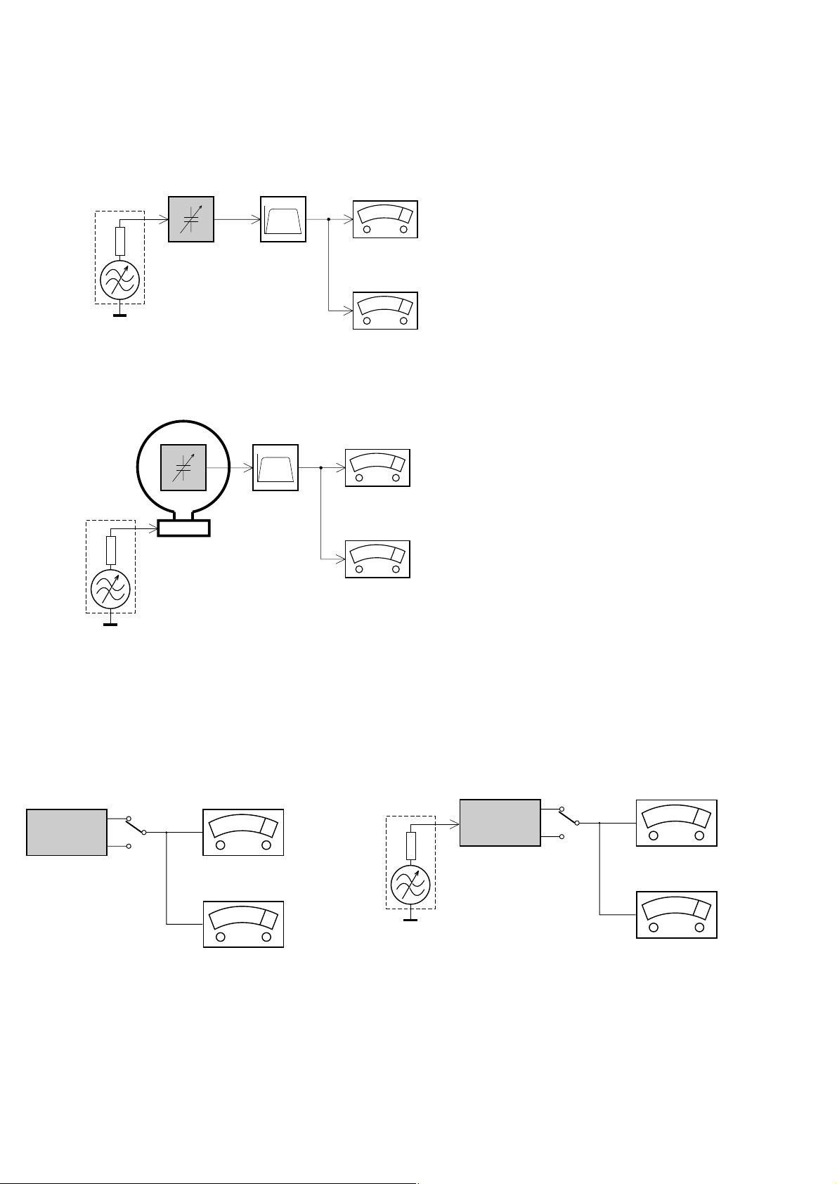
MEASUREMENT SETUP
Tuner FM
1-4
Bandpass
LF Voltmeter
e.g. PM2534
RF Generator
e.g. PM5326
DUT
250Hz-15kHz
e.g. 7122 707 48001
Ri=50Ω
S/N and distortion meter
e.g. Sound Technology ST1700B
Use a bandpass filter to eliminate hum (50Hz, 100Hz) and disturbance from the pilottone (19kHz, 38kHz).
Tuner AM (MW,LW)
RF Generator
e.g. PM5326
Ri=50Ω
DUT
Frame aerial
e.g. 7122 707 89001
Bandpass
250Hz-15kHz
e.g. 7122 707 48001
LF Voltmeter
e.g. PM2534
S/N and distortion meter
e.g. Sound Technology ST1700B
To avoid atmospheric interference all AM-measurements have to be carried out in a Faraday´s cage.
Use a bandpass filter (or at least a high pass filter with 250Hz) to eliminate hum (50Hz, 100Hz).
CD
Use Audio Signal Disc
(replaces test disc 3)
DUT
L
R
SBC429 4822 397 30184
S/N and distortion meter
e.g. Sound Technology ST1700B
LEVEL METER
e.g. Sennheiser UPM550
with FF-filter
Recorder
Use Universal Test Cassette CrO2 SBC419 4822 397 30069
or Universal Test Cassette
LF Generator
e.g. PM5110
Fe SBC420 4822 397 30071
DUT
L
R
S/N and distortion meter
e.g. Sound Technology ST1700B
LEVEL METER
e.g. Sennheiser UPM550
with FF-filter
Page 5
SERVICE AIDS
Service Tools:
Universal Torx driver holder .................................. 4822 395 91019
Torx bit T10 150mm ............................................. 4822 395 50456
Torx driver set T6 - T20 ......................................... 4822 395 50145
Torx driver T10 extended ...................................... 4822 395 50423
Compact Disc:
SBC426/426A Test disc 5 + 5A ............................ 4822 397 30096
SBC442 Audio Burn-in Test disc 1kHz ................. 4822 397 30155
SBC429 Audio Signals disc .................................. 4822 397 30184
Dolby Pro-logic Test Disc ...................................... 4822 395 10216
1-5
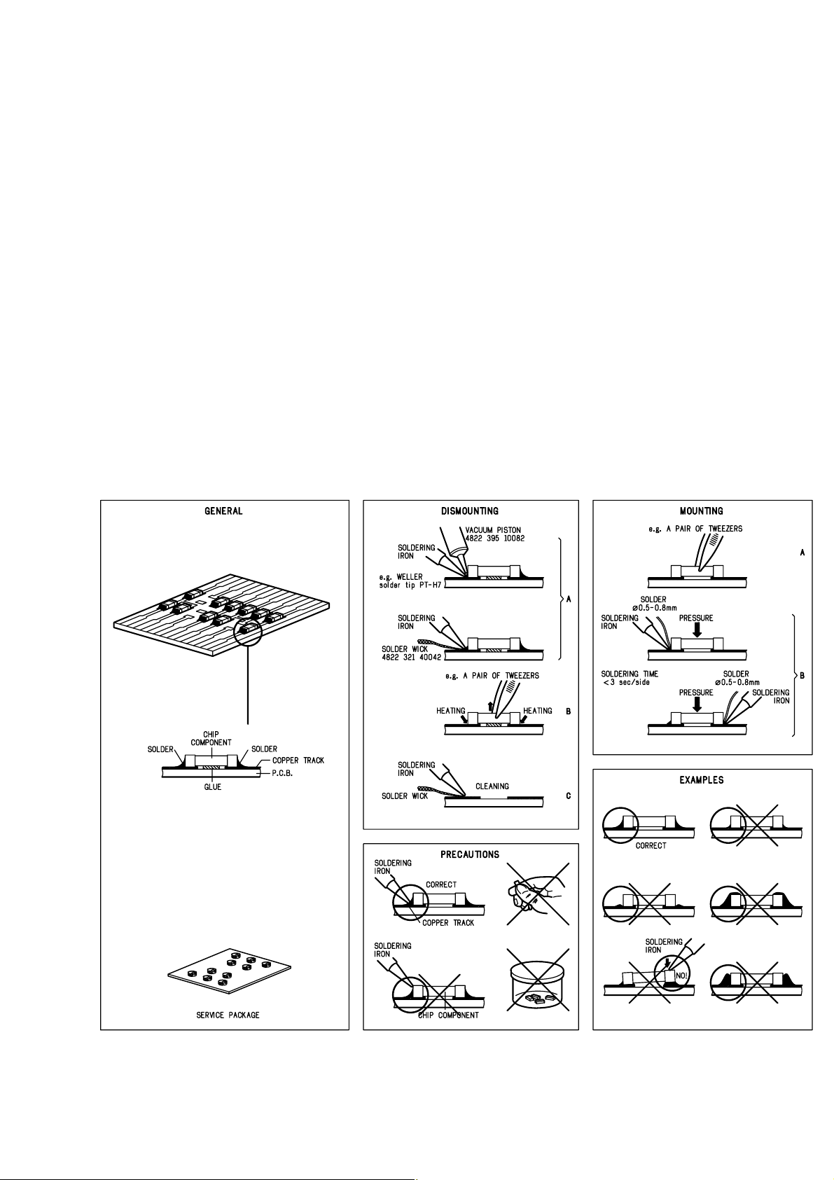
HANDLING CHIP COMPONENTS
Page 6
1-6
GB
All ICs and many other semi-conductors are
susceptible to electrostatic discharges (ESD).
Careless handling during repair can reduce life
drastically.
When repairing, make sure that you are
connected with the same potential as the mass
of the set via a wrist wrap with resistance.
Keep components and tools also at this
potential.
Tous les IC et beaucoup d’autres
semi-conducteurs sont sensibles aux
décharges statiques (ESD).
Leur longévité pourrait être considérablement
écourtée par le fait qu’aucune précaution n’est
prise à leur manipulation.
Lors de réparations, s’assurer de bien être relié
au même potentiel que la masse de l’appareil et
enfiler le bracelet serti d’une résistance de
sécurité.
Veiller à ce que les composants ainsi que les
outils que l’on utilise soient également à ce
potentiel.
F
WARNING
ATTENTION
GB
Complete Kit ESD3 (small tablemat, wristband,
connection box, extention cable and earth cable) ...........4822 310 10671
Wristband tester ....................................................................4822 344 13999
ESD
D
WARNUNG
Alle ICs und viele andere Halbleiter sind
empfindlich gegenüber elektrostatischen
Entladungen (ESD).
Unsorgfältige Behandlung im Reparaturfall kan
die Lebensdauer drastisch reduzieren.
Veranlassen Sie, dass Sie im Reparaturfall über
ein Pulsarmband mit Widerstand verbunden
sind mit dem gleichen Potential wie die Masse
des Gerätes.
Bauteile und Hilfsmittel auch auf dieses gleiche
Potential halten.
ESD PROTECTION EQUIPMENT:
NL
Alle IC’s en vele andere halfgeleiders zijn
gevoelig voor electrostatische ontladingen (ESD).
Onzorgvuldig behandelen tijdens reparatie kan
de levensduur drastisch doen verminderen.
Zorg ervoor dat u tijdens reparatie via een
polsband met weerstand verbonden bent met
hetzelfde potentiaal als de massa van het
apparaat.
Houd componenten en hulpmiddelen ook op
ditzelfde potentiaal.
Tutti IC e parecchi semi-conduttori sono
sensibili alle scariche statiche (ESD).
La loro longevità potrebbe essere fortemente
ridatta in caso di non osservazione della più
grande cauzione alla loro manipolazione.
Durante le riparazioni occorre quindi essere
collegato allo stesso potenziale che quello della
massa dell’apparecchio tramite un braccialetto
a resistenza.
Assicurarsi che i componenti e anche gli utensili
con quali si lavora siano anche a questo
potenziale.
WAARSCHUWING
I
AVVERTIMENTO
GB
Safety regulations require that the set be restored to its original
condition and that parts which are identical with those specified,
be used
Safety components are marked by the symbol
!
.
NL
Veiligheidsbepalingen vereisen, dat het apparaat bij reparatie in
zijn oorspronkelijke toestand wordt teruggebracht en dat onderdelen,
identiek aan de gespecificeerde, worden toegepast.
De Veiligheidsonderdelen zijn aangeduid met het symbool
!
F
Les normes de sécurité exigent que l’appareil soit remis à l’état
d’origine et que soient utiliséés les piéces de rechange identiques
à celles spécifiées.
Less composants de sécurité sont marqués
!
D
Bei jeder Reparatur sind die geltenden Sicherheitsvorschriften zu
beachten. Der Original zustand des Geräts darf nicht verändert werden;
für Reparaturen sind Original-Ersatzteile zu verwenden.
Sicherheitsbauteile sind durch das Symbol
!
markiert.
I
Le norme di sicurezza esigono che l’apparecchio venga rimesso
nelle condizioni originali e che siano utilizzati i pezzi di ricambio
identici a quelli specificati.
Componenty di sicurezza sono marcati con
!
CLASS 1
LASER PRODUCT
GB
Invisible laser radiation when open.
Avoid direct exposure to beam.
Osynlig laserstrålning när apparaten är öppnad och spärren
är urkopplad. Betrakta ej strålen.
SF
Avatussa laitteessa ja suojalukituksen ohitettaessa olet alttiina
näkymättömälle laserisäteilylle. Älä katso säteeseen!
DK
Usynlig laserstråling ved åbning når sikkerhedsafbrydere er
ude af funktion. Undgå udsaettelse for stråling.
S
Warning !
Varning !
Varoitus !
Advarse !
GB
After servicing and before returning set to customer perform a leakage
current measurement test from all exposed metal parts to earth ground to
assure no shock hazard exist. The leakage current must not exceed
0.5mA.
F
"Pour votre sécurité, ces documents doivent être utilisés par
des spécialistes agréés, seuls habilités à réparer votre
appareil en panne".
Page 7
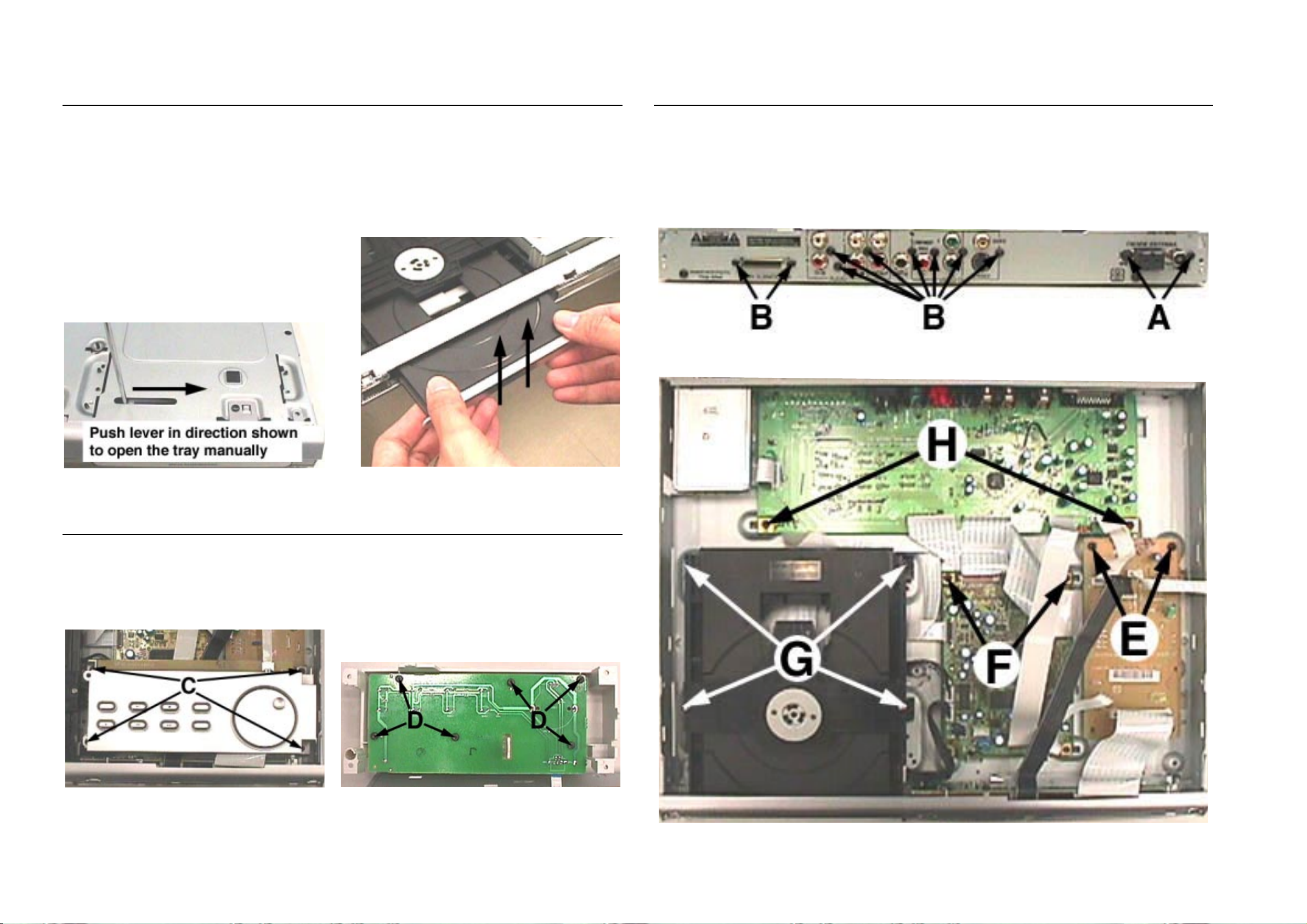
DISMANTLING INSTRUCTIONS
2-1 2-1
Dismantling of the DVD Loader
1) The tray can be manually open by inserting a minus
screw driver and push the lever in the direction as shown
in Figure 1 to unlock the tray before sliding it out.
2) Slide out the tray and remove the Cover Tray (pos 110)
as shown in Figure 2.
3) Loosen 2 screws each to remove the Panel Cover Left
(pos 231) and Panel Cover Right (pos 232).
4) Loosen 3 screws to remove the Front Top (pos 240).
- 1 screw each on the left & right side (pos 272)
- 1 screw at the bottom (pos 268)
5) Loosen 4 screws G (see Figure 6) to remove the DVD
Loader (pos 1602).
Dismantling of the Tuner Module, AV Board, Front Board and SD6.3 ST AV2 Board
1) Loosen 2 screws A (see Figure 5) to remove the Tuner
Module (pos 1801).
2) Loosen 9 screws B (see Figure 5) and 2 scews H (see
Figure 6) to remove the AV Board (pos 1501).
Figure 5
3) Loosen 2 screws E (see Figure 6) to remove the Front
Board (pos 1201).
4) Loosen 2 screws F (see Figure 6) to remove the SD6.3
ST AV2 Board (1601).
Dismantling of the Front Key Board
1) Loosen 4 screws C (see Figure 3) to remove the Bracket
Support Control (pos 130) and the Front Key Board (pos
1401).
Figure 2Figure 1
2) Loosen 6 screws D (see Figure 4) to remove the Front
Key Board (pos 1401) from the Bracket Support Control
(pos 130).
Figure 3
Figure 4
Figure 6
Page 8
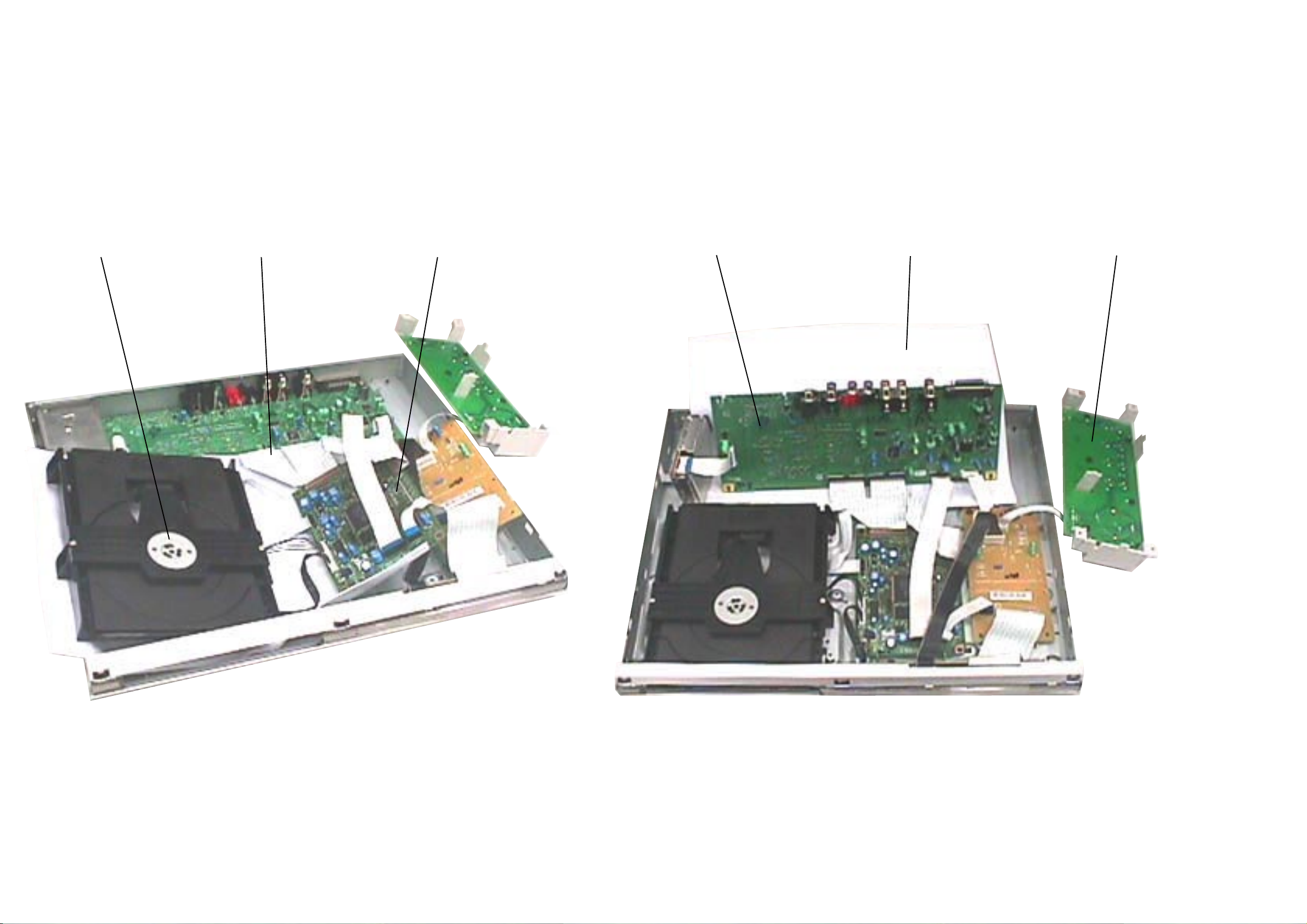
SERVICE POSITIONS
2-2
2-2
SD6.3 ST AV2 BoardDVD Loader Thick Insulation Sheet Front Key BoardThick Insulation Sheet
AV Board
Page 9
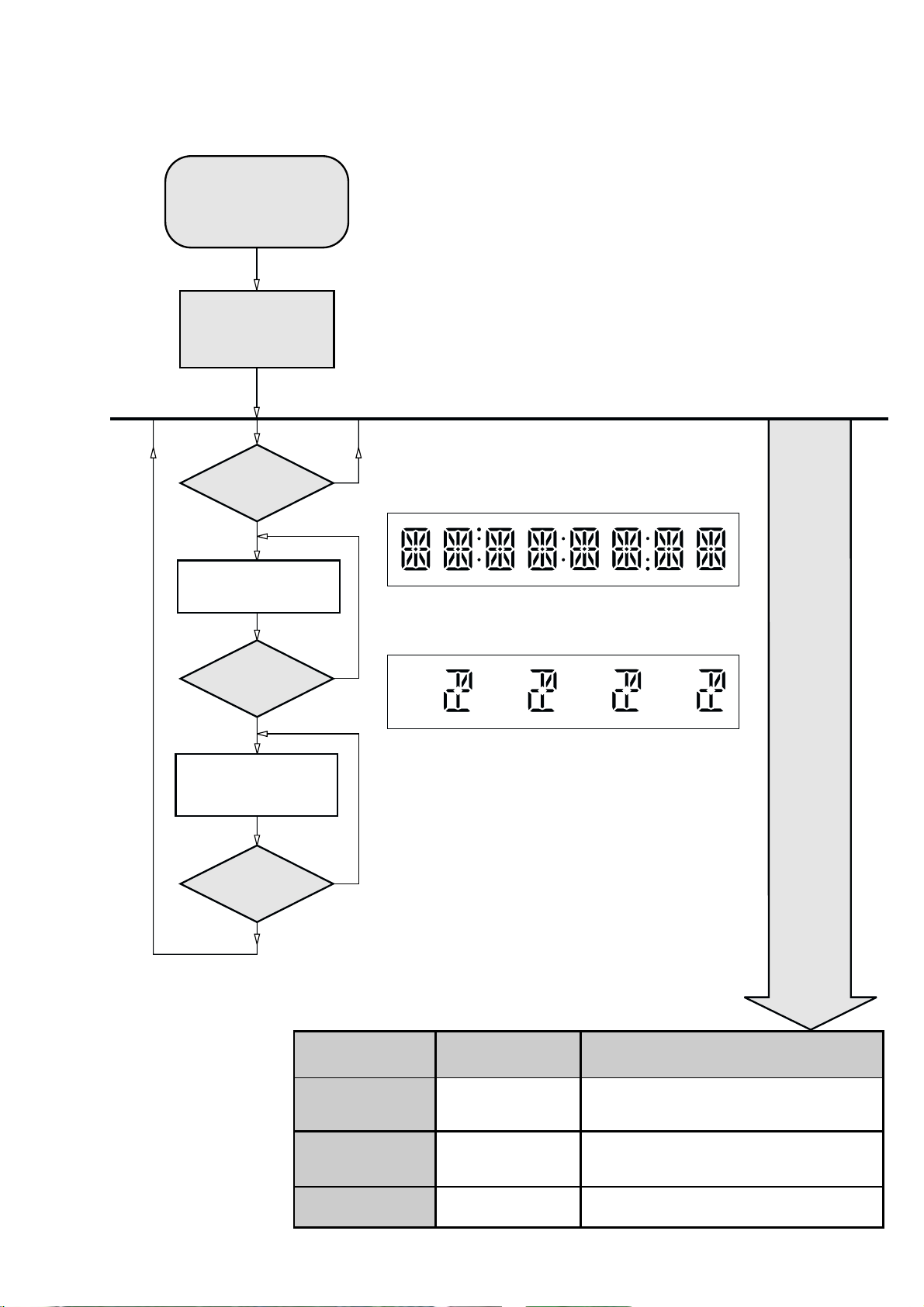
SERVICE TEST PROGRAM
3-1
To start service test program
hold BII and
buttons depressed while
plugging in the mains cord
Display shows
"SERVICE"
followed by ROM version
"S-Vxx-yy"
S
MAIN MENU
DISPLAY
TEST
BII
Button pressed?
Y
Display shows Figure 1
and switch "SACD" LED on
Hold BII and buttons depressed
S refers to Service Mode
V refers to Version
xx refers to Software version number of BEA
(counting up from 01 to 99)
yy refers to Software version number of Front uP
(counting up from 01 to 99)
N
S
Figure 1
till the Display shown "S-Vxx-yy"
BII
Button pressed?
Y
Display shows Figure 2
and switch "SACD" LED off
9
Button pressed?
Y
TEST
EEPROM FORMAT
TEST
ROTARY
ENCODER TEST
LEAVE SERVICE
TEST PROGRAM
N
Figure 2
N
Various
other Tests
Activated with
S
S to Exit
Volume
Knob
Disconnect
mains cord
ACTION
Load default data. Display shows "NEW".
Caution!
All presets from the customer will be lost!!
Display shows value for 2 seconds.
Volume values increases or decreases in steps of 1
until 0 (VOL MIN) or 40 (VOL MAX) is reached.
LX8300SA & LX8320SA & LX8500W_Service Test Program_dd wk0429
Page 10

3-2
Reprogramming of DVD version Matrix
After repair, the customer setting and region code may be
lost. Reprogramming will put the set back in the state in
which it has left the factory, ie. with the default setting and
the allowed region code.
Model Region Region Code TV Type
LX8300SA/01 Europe 2 PAL
LX8300SA/05 Europe 2 PAL
LX8320SA/69 AP 3 PAL
LX8300SA/04 Russia 5 PAL
LX8320SA/93 China 6 PAL
LX8500W/01 Europe 2 PAL
LX8500W/04 Russia 5 PAL
LX8500W/69 AP 3 PAL
LX8500W/93 China 6 PAL
To reprogram do as follows:
1) Power up the set and select DISC source.
2) Open tray by press "OPEN/CLOSE" button on the set
or press and hold "STOP" button on the RC.
3) Press the following buttons on the Remote Control:
<9> <9> <9> <9> <AUDIO> <1> ......... for LX8300SA/01
<9> <9> <9> <9> <AUDIO> <2> ......... for LX8300SA/05
<9> <9> <9> <9> <AUDIO> <3> ......... for LX8320SA/69
<9> <9> <9> <9> <AUDIO> <4> ......... for LX8300SA/04
<9> <9> <9> <9> <AUDIO> <5> ......... for LX8320SA/93
<9> <9> <9> <9> <AUDIO> <6> ...........for LX8500W/01
<9> <9> <9> <9> <AUDIO> <7> ...........for LX8500W/04
<9> <9> <9> <9> <AUDIO> <8> ...........for LX8500W/69
<9> <9> <9> <9> <AUDIO> <9> ...........for LX8500W/93
4) The display shows 'YYYY-ZZ' and the tray will close.
YYYY = model number (eg. 8300, 8500, etc.)
ZZ = slash stroke version (eg. 01, 69, etc.)
Procedure for check Software version
1) Power up the set and select DISC source.
2) Open tray by press "OPEN/CLOSE" button on the set
or press and hold "STOP" button on the RC.
3) Press "DISPLAY" button on the Remote control.
4) The TV screen will shows:
SD6.3 Vxx YYYY-ZZ A BB
SERVO: nnnnnnnn REG:A
xx = version number
YYYY = model number (eg. 8300, 8500, etc.)
ZZ = slash stroke version (eg. 01, 69, etc.)
A = region code
BB = Front uP software version number
nnnnnnnn = servo version number
Procedure to upgrade software
1) Power up the set and select DISC source.
2) Open tray by press "OPEN/CLOSE" button on the set
or press and hold "STOP" button on the RC.
3) Place upgrade CD-ROM onto tray and close.
4) The set will response and display the following:
- LOAD [After the disc is read, the tray will open for
you to remove the disc]
- ERASE [Erasing disc]
- WRITE [Writing disc]
- ERROR [if upgrade is unsuccessful]
- UPG END [if upgrade is successful]
- DISC->CLOSE->LOAD [Tray will close indicating that
the upgrade process is completed]
5) The whole process should not take more than 5
minutes.
Caution: Do not unplug the set until upgrade is completed.
Trade Mode
Trade mode is a feature that will block all set keys when
enabled. It is for dealers to prevent customers from
removing disc, changing source etc using the set keys.
Rotary and Remote Control (RC) keys are still allowed in
Trade mode.
To activate Trade Mode:
1) Power up the set and select DISC source.
2) Open tray by press "OPEN/CLOSE" button on the set
or press and hold "STOP" button on the RC.
3) Then press buttons <2> <5> <9> on the RC.
4) The display shows 'TRA ON' and the tray will close.
Trade Mode is now enabled.
To deactivate Trade Mode:
1) Power up the set and select DISC source.
2) Open tray by press and hold "STOP"button on the RC.
3) Then press buttons <2> <5> <9> on the RC.
4) The display shows 'TRA OFF' and the tray will close.
Trade Mode is now disabled.
Procedure to change Tuner Grid (not for all versions)
1) By holding "SOURCE" and "PREV" buttons depressed
while switching on the mains supply, the tuning grid
frequency is toggled between 9kHz and 10kHz.
2) Hold the "SOURCE" and "PREV" buttons depressed
until the display shown the new tuning grid 'GRID 9' or
'GRID 10'.
Note: Repeating the same action will toggle back to its
previous tuning grid setting.
Page 11
SET BLOCK DIAGRAM
4-1
4-1
10K
TUNER
(TM 08)
74HC4052
1n0
UCD
L/R
POWER AMP
RDS IC
SAA6581T
10K
M62320FP
*
CS2
CS1
CS0
SCL
SDA
VDD
GND
CHIP SELECT
I2C BUS
TRANSCEIVER
PWR
OUT I/O IN
RES
D5
D6
D7
SHIFT
REG
8
88
DATA LATCHES
88 8
I/O PORT
D4
D1
D2
D3
SO
D0
SCL
SDA
UCD
UCD
UCD
SURROUND
POWER AMP
IN
L7808
GND
2
4
5
C
A
B
3
1
VS
OUT
GND
OUT
8MHz
Block Diagram_LX8500W_dd wk0428
Page 12
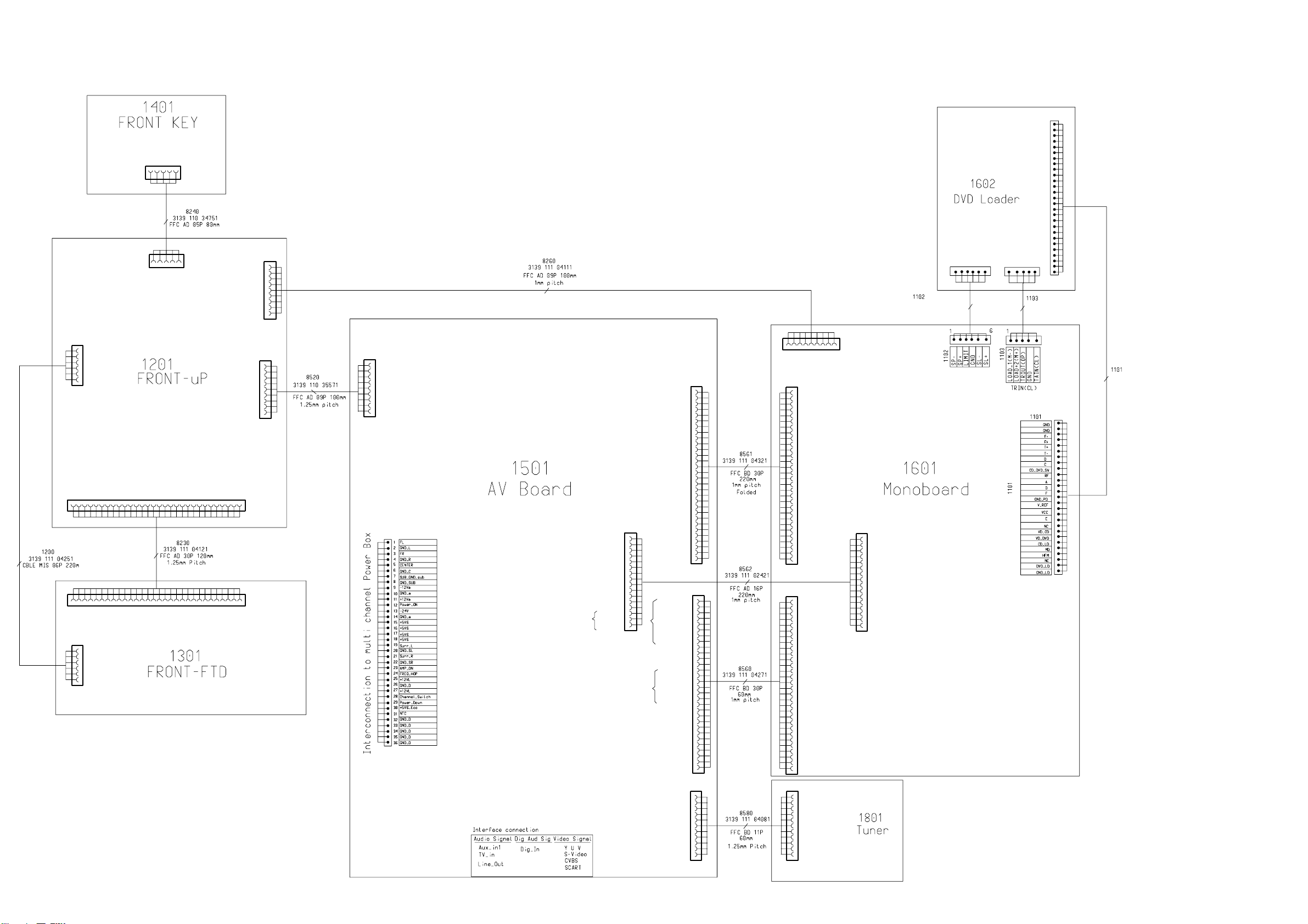
SET WIRING DIAGRAM
voIB
1
1300
voIA
5-1
key1
key0
GND_D
3
4
5
2
5-1
26
EH
1101
1G
1
2
1201
1
SFW30R-2STE1
1G
0200
Dipmate
1
2
3
4
5
6
3G
3
2
3
3G
2G
1
2
3
4
5
6
+5VDSTBY
ioRC6
GND_D
STDBY_LED
+5VL
SACD_LED
4G
5G6G7G
456
456
4G
5G
6G
+5VDSTBY
ioRC6
GND_D
STDBY_LED
+5VL
SACD_LED
1100
2
345
1
key0
voIA
voIB
key1
GND_D
+5V6_ECO
Channel Switch
ioIIC_Data_Wireless
1107
SFW30R-2STE1
P3
P2
P5
P4
P8
P72GP6
11
P15
P13
P14
121314
12
13
P13
P14
P9
P12
P11
P10
15
161718
19
161718
19
15
14
P8
P7
P9
P11
P12
P10
8G
P16
P17
P15
7
8
9
10
11
7
8
9
10
7G
8G
P16
P17
21222324252627
20
21
22
20
23
24
P2
P3
P4
P5
P6
P1
GND
V_FL
+12VL
28
27
26
25
28
P1
GND
V_FL
+12VL
FP_IRQ
SDA
SCL
GND_D
Stdby
VolA
VolB
09FMN-BTRK-A
+5V6
+12VL
GND_D
GND_D
-33V
NTC
GND
40kHz
29
30
29
30
GND
40kHz
1103
1
2
3
4
5
NC
6
IR
7
8
9
1105
2
1
4
3
6
7
5
8
1102
1
2
3
4
5
6
7
8
9
1507
1
2
3
4
5
6
7
8
9
+5V6
+12VL
GND_D
+5V6_ECO
Channel Switch
GND_D
ioIIC_Data_Wireless
-33V
NTC
1509
To control
DAC
GND_D
GND_D
+1V8
+1V8
+5VL
+5VL
+5VL
GND_D
GND_D
PWR_ON
RDS_DAT
VSCK
VSDA
GND_D
1
2
3
+8V
4
5
6
7
8
9
10
+8V
11
12
13
14
15
16
16FNM-STK-A
1511
Data for
To Tuner
GND_D
Tu_SD
S1_L3_1
S0_L3_0
AV_Mute
GND_D
GND_D
GND_D
CVBS
GND_D
GND_D
B_Cb
GND_D
GND_D
PCM_BCLK
PCM_LTRT
GND_D
PCM_MCLK
PCM_LRCK
GND_D
SPDIF_OUT
GND_D
PCM_MIC_IN
GND_D
MIC_DET
GND_D
PCM_LR
GND_D
PCM_LsRs
GND_D
PCM_CLfe
GND_D
PCM_Cs
GND_D
ADC
SCL_DAC
SDA_DAC
GND_D
TU_SD
TU_CE
TU_DI
TU_DO_ST
TU_CLK
GND_D
SPDIF_IN
SPDIF_GND
AMP_On
Mute_TV
PW_DN
Freq_Hop
HP_Det
GND_D
RDS_CLK
RDS_DAT
GND_D
GND_a
Tu_SD
RDS_Mux
Tu_CE
Tu_DI
Tu_DO_ST
Tu_CLK
1
2
3
L2
4
5
6
7
8
Y
9
10
C
11
12
13
G_Y
14
15
16
17
R_Cr
18
19
20
21
22
23
24
25
26
27
28
29
30
SFW30R-2STE1
ERR
SFW30R-2STE1
11
NC
10
9
8
+9V1
7
Rch
6
5
4
Lch
3
2
1
11FE-BT-VK-N11FE-BT-VK-N
SCL
SDA
FP_IRQ
1401
1200
1
2
3
4
5
6
7
8
9
10
11
12
13
14
15
16
17
18
19
20
21
22
23
24
25
26
27
28
29
30
1100
1301
1
2
3
4
5
6
7
8
9
10
11
12
13
14
15
16
17
18
19
20
21
22
23
24
25
26
27
28
29
30
SFW30R-2STE1
1302
SFW30R-2STE1
CN1
11FE-BT-VK-N
10
11
12
13
14
15
16
17
18
19
20
21
22
23
24
25
26
27
28
29
30
1
2
3
4
5
6
7
8
9
10
11
IR
GND_D
PCM_LRCLK
GND_D
Tu_SD
L2
S1_L3_1
S0_L3_0
AV_Mute
GND_D
Y
GND_D
C
GND_D
CVBS
GND_D
G_Y
GND_D
B_Cb
GND_D
R_Cr
GND_D
PCM_SCLK
PCM_LTRT
GND_D
PCM_MCLK
PCM_LRCK
GND_D
SPDIF_OUT
GND_D
PCM_MIC_IN
GND_D
MIC_DET
1
GND_D
2
PCM_LR
3
GND_D
PCM_LsRs
4
5
GND_D
6
PCM_CLfe
7
GND_D
PCM_Cs
8
GND_D
9
SCL_DAC
SDA_DAC
GND_D
TU_SD
TU_CE
TU_DI
TU_DO_ST
TU_CLK
GND_D
SPDIF_IN
GND_D
ERR
AMP_On
Mute_TV_
PW_DN_
Freq_Hop
HP_Det
GND_D
RDS_CLK
RDS_DAT
GND_D
GND_a
NC
Tu_SD
+9V1
NC
Rch
Tu_CE
Lch
Tu_DI
Tu_DO_ST
Tu_CLK
VolA
Stdby_ctrl
9
09FMN-BTRK-A
VolB
16FNM-STK-A
1104
1
2
3
4
5
6
7
8
9
10
11
12
13
14
15
16
GND_D
GND_D
+8V
+1V8
+1V8
+5VL
+5VL
+5VL
GND_D
+8V
GND_D
PWR_ON
RDS_DAT
VSCK
VSDA
GND_D
3139 111 04311
CBLE PH 06P/100/06P
PH 28ST BK
3139 110 27831
CBLE PH 05P/120/05P
PH 260S BK
1
3139 241 00851
FFC FOIL 24P/180/24P
AD 0.5MMP
26
1
Wiring Diagram_3139 119 38131_dd wk0428
Page 13
6-1 6-1
FTD DISPLAY PIN CONNECTION
8G 7G 6G 5G 4G 3G 2G 1G
PANEL FRONT BOARDS
TABLE OF CONTENTS
FTD Display Pin Connection ........................................... 6-1
Front Board - Component & Chip Layout ........................ 6-2
Front Board - Circuit Diagram ......................................... 6-3
IR/FTD/LED Board - Component & Chip Layout ............ 6-4
IR/FTD/LED Board - Circuit Diagram .............................. 6-5
Front Key Board - Component & Chip Layout ................ 6-6
Front Key Board - Circuit Diagram .................................. 6-7
Electrical parts list............................................................ 6-7
P1
P2
P3
P4
P5
P6
P7
P8
P9
P10
P11
P12
P13
P14
P15
P16
P17
8G
Dp2
col3
col2 Dp1
col1
a
j
h
f
g
e
r
k
b
p
m
j
n
c
( 1G - 8G )
d
7G
a
k
j
h
b
f
m
p
g
c
e
n
r
-
d
-
-
a
k
j
h
b
f
m
p
g
c
e
n
r
col3
d
-
Dp2
6G
a
k
j
h
b
f
m
p
g
c
e
n
r
d
-
5G
a
k
j
h
b
f
m
p
g
c
e
n
r
col2
d
-
-
4G
3G
a
k
j
h
b
f
m
p
g
c
e
n
r
d
-
-
a
k
j
h
b
f
m
p
g
c
e
n
r
d
-
2G
a
k
j
h
b
f
m
p
g
c
e
n
r
col1
d
-
Dp1
1G
a
k
j
h
b
f
m
p
g
c
e
n
r
-
d
-
-
Page 14
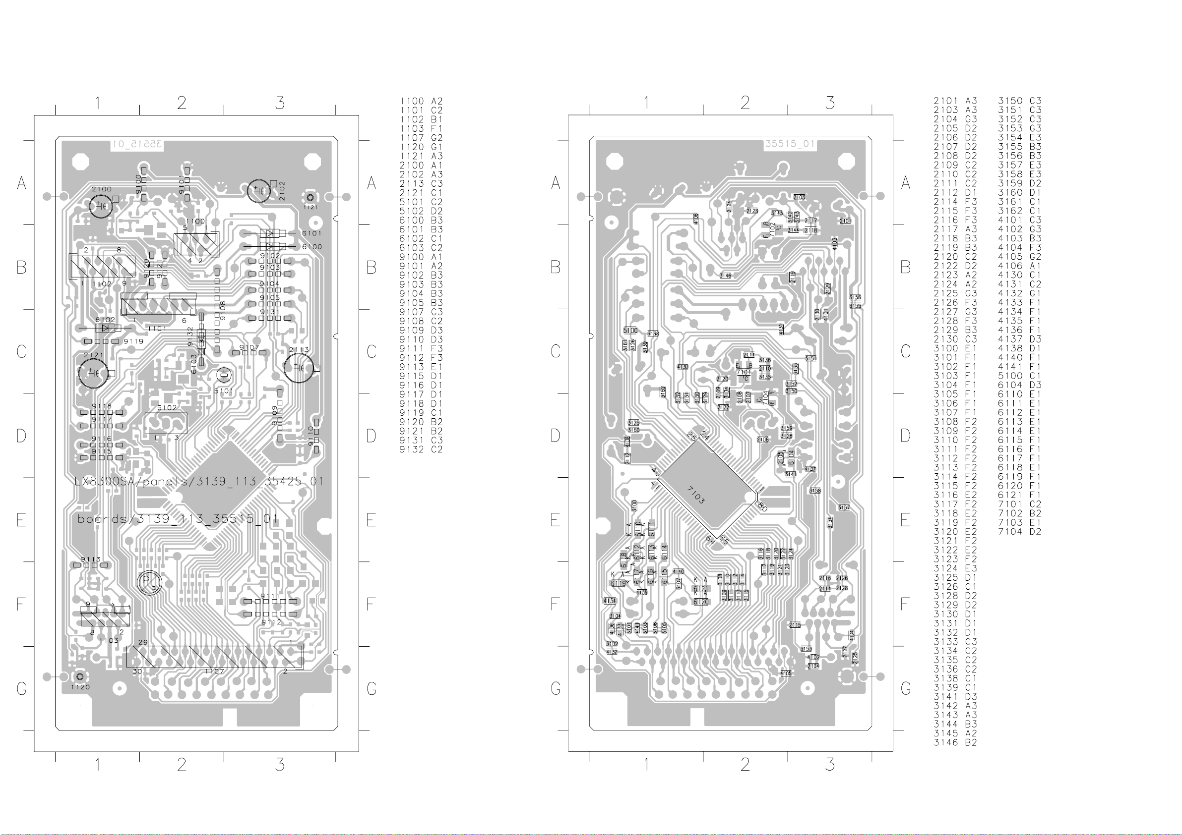
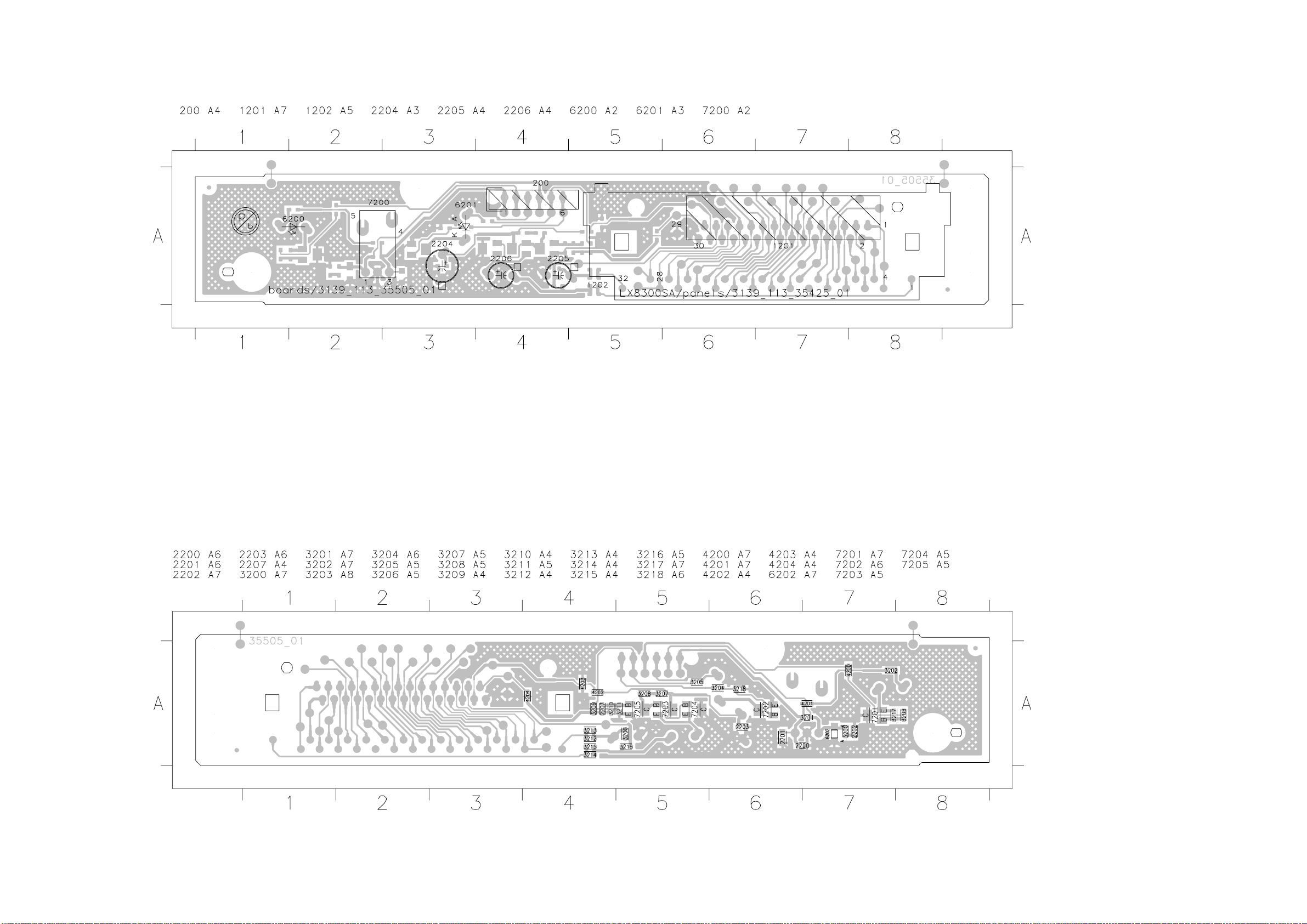
6-2
FRONT BOARD - COMPONENT LAYOUT FRONT BOARD - CHIP LAYOUT
6-2
This assembly drawing shows a summary of all possible versions.
For components used in a specific version see schematic diagram and respective parts list.
This assembly drawing shows a summary of all possible versions.
For components used in a specific version see schematic diagram and respective parts list.
3139 113 3551 pt5 dd wk0428
3139 113 3551 pt5 dd wk0428
Page 15
FRONT BOARD - CIRCUIT DIAGRAM
G
6-3 6-3
12345678910111213
40kHZ
V_FIL
+12VL
A
uP BOARD
7
8
ioKey1
2123
05FE-BT-VK-N
B
C
5
4
3
2
1
B6B-EH-A
1101
1
2
3
4
5
6
1100
2126
330p
+5VDSTBY
ioRC6
stdy
+5VL
SACD_LED
VolB
2125
330p
VolA
2124
330p
ioKey0
330p
30
29
25
26
27
28
D
4101
4103
330p
2115
1N4148
-VKK
NTC
330p
2128
6100
6101
1N4148
2116
2129
2130
IR
330p
+5V6ECO
330p
330p
330p
3157
100R
2102
+5V6
Wireless
25V47u
2103
1N4148
ioIIC_Data_Wireless
3153
100R
3158
100R
stdy
+5VDSTBY
100n
6102
3154
100R
3155
10K
3156
10K
2100
+5VL
3150
2104
22n
4102
+5VL
2101
100n
47u 25V
-Vkk
+5VL
10K
4K7
4K7
3151
3152
ioIIC_Data
ioIIC_Clk
ioIIC_IntReq
6104
3141
BZX384-C4V7
V_FIL
10K
1102
FE-BT-VK-N
1
2
+12VL
3
4
E
5
6
7
8
FROM AV PCB
9
F
2119
330p
2114
1103
1
VSTB
2
VSDA
3
VSCK
4
GND_MTK
5
2127
H
6
7
8
VOLA
9
VOLB
330p
09FMN-BTRK-A
VolA
VolB
3119
3121
3122
3123
3124
2105
21
3116
3117
3118
47n
2121
1K0
3120
1K0
1K0
1K0
1K0
1K0
20
18
19
15
16
17
3115
3114
1K0
1K0
14
3113
1K0
3112
1K0
12
13
3111
1K0
7103
1K0
1K0
1K0
65
66
67
68
69
70
71
72
73
74
75
76
77
78
79
50V 47u
V24
V25
V26
V27
V28
V29
V30
V31
V32
V33
V34
V35
V36
VKK
-SCK1
SI1
1
V23
SO1
V21
V20
V22
8-Bit h. break. v.
80k pull
down
8-Bit h. breakdown v.
out. port w. latch P9
PD
source open
drain 80k p.d.
5-Bit h. breakd. v.
out w. latch
8-Bit Input/Output
(tri-state)
P04
P05
P03
4
3
V19
P06
22
23
24
I
1234567
9
10
11
3109
3108
3110
1K0
1K0
1K0
585966061626364
V16
V17
V18
VFT driver circuit (automatic display)
P0
VSS
XOUT
P07
8809
7
4K7
3128
5102
22p
2106
2107
10K
3159
8 9 10 11 12 13
6
V13
V14
V15
8-Bit high breakdown voltage 8-Bit high breakdown v.
output port with latch output port with latchout w. latch P8
sink o.
8-Bit I/O P2
XIN
-RESET
XTOUT
11 12 13
10
22p
2122
2p2
2108
22p
7104
BC847B
3
4
5
1
2
1107
6117
BAS316
6118
BAS316
6116
BAS316
6119
6120
BAS316
BAS316
6121
BAS316
6115
6114
6112
6113
1K0 3107
BAS316
BAS316
BAS316
BAS316
V5
V6
V7
V8
V9
V11
V10
V12
P7 P6
80k pull down80k pull down
P6-P9 source open drain
ROMRAM
CPU
sink o.drain
XTIN
Program
Counter
8-Bit A/D
Converter
drain
8-Bit Input/Output
(tri state)
TEST
14 15 16 17 18 19220 21 22 23 24
-STOP
-INT0
-INT1
TC2
-DV0
TC4
100R
3129
5101
32K768
22p
stdy
2120
3134
1K0
7101
BC847B
10n
2109
2110
6111
BAS316
V4
80k pull down
P1
TC1
3162
1K0
40kHz
2111
10n
3135
3100
6110
1K0
BAS316
4344454647484955051525354555657
V2
V3
3-B. I/O P3
( tristate )
INT4
INT2
100R
3131
3130
470n
3136
100K
SIN-01T-1.8
1121
1
3101
82K
3102
82K
82K
3103
310482K
310582K
3106
82K
4142
V1
V0
VDD
VAREF
VASS
AIN13
P5
AIN12
AIN11
AIN10
4-Bit In/Output
(tri-state)
AIN7
P4
AIN6
AIN5
AIN4
AIN3
8-Bit Input/Output
AIN2
(tri-state)
AIN1
AIN0
-SCKO
SCA
SCL
22R
3133
1K0
22R
3132
6103
1N4148
9132
100K
40
39
38
37
36
35
34
33
32
31
30
29
28
27
26
25
+5VDSTBY
3161
SIN-01T-1.8
1120
-Vkk
1K0
1K0 3125
1K0
31261K0
ioIIC_Data
ioIIC_Clk
ioRC6
5100
2u2
1
3142
100R
9131
2117
ioRC6
2112
3160
SACD_LED
ioIIC_IntReq
+5VDSTBY
100n
2118
100n
2113
ioIIC_Data_Wireless
Wireless
NTC
7102
BC847B
3144
4u7
1K2
10K
3143
3145
47K
+5VDSTBY
100u 10V
+5VDSTBY
2K7
2K7
3138
3139
ioKey1
ioKey0
3139 113 35425_3139 113 3551 pt5_dd wk0428
IR
3146
10K
1100 B1
1101 C1
1102 D1
1103 G2
1107 A9
1120 B11
1121 B11
2100 E4
2101 E4
2102 D3
A
2103 D3
2104 H4
2105 G6
2106 H8
2107 H8
2108 H8
2109 I9
2110 I10
2111 I10
2112 E11
2113 E12
2114 G2
B
2115 G2
2116 G2
2117 C11
2118 C12
2119 F1
2120 H9
2121 G7
2122 H9
2123 B4
2124 B3
2125 B3
C
2126 C2
2127 H1
2128 H2
2129 E2
2130 F2
3100 D10
3101 C10
3102 C10
3103 C10
3104 C10
3105 C10
3106 D10
D
3107 D9
3108 D8
3109 D8
3110 D8
3111 D8
3112 D8
3113 D7
3114 D7
3115 D7
3116 E7
3117 E7
3118 E7
E
3119 E6
3120 E7
3121 E6
3122 E6
3123 F6
3124 F6
3125 F11
3126 F11
3128 G8
3129 G9
3130 H10
F
3131 H10
3132 H10
3133 G10
3134 H9
3135 I10
3136 I10
3138 F12
3139 F12
3141 G6
3142 B11
3143 C12
3144 C12
G
3145 C12
3146 C13
3150 G4
3151 G4
3152 G4
3153 G3
3154 G4
3155 H4
3156 I4
3157 H3
3158 H3
3159 I8
H
3160 F11
3161 F11
3162 G10
4101 E2
4102 H4
4103 E2
5100 H11
5101 H9
5102 H8
6100 D2
6101 D2
I
6102 E3
6103 H11
6104 G6
6110 D10
6111 D10
6112 D10
6113 D9
6114 D9
6115 D9
6116 C9
6117 C10
6118 C10
6119 C9
6120 C9
6121 D9
7101 I10
7102 B13
7103 D7
7104 I8
9131 F11
9132 I11
Page 16
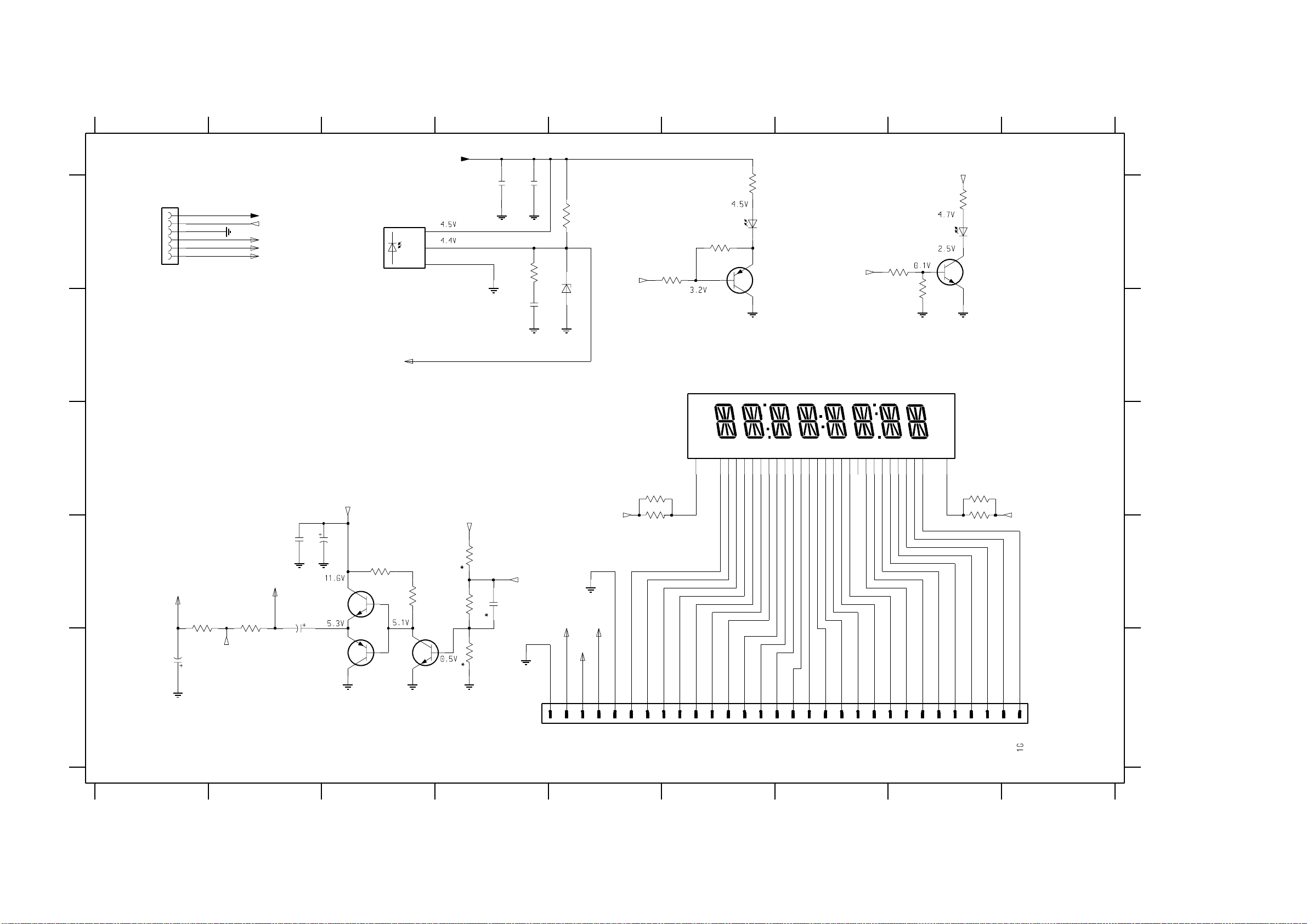
IR/FTD/LED BOARD - COMPONENT LAYOUT
This assembly drawing shows a summary of all possible versions. For components used in a specific version see schematic diagram and respective parts list.
6-4
6-4
3139 113 3550 pt5 dd wk0428
IR/FTD/LED BOARD - CHIP LAYOUT
This assembly drawing shows a summary of all possible versions. For components used in a specific version see schematic diagram and respective parts list.
3139 113 3550 pt5 dd wk0428
Page 17
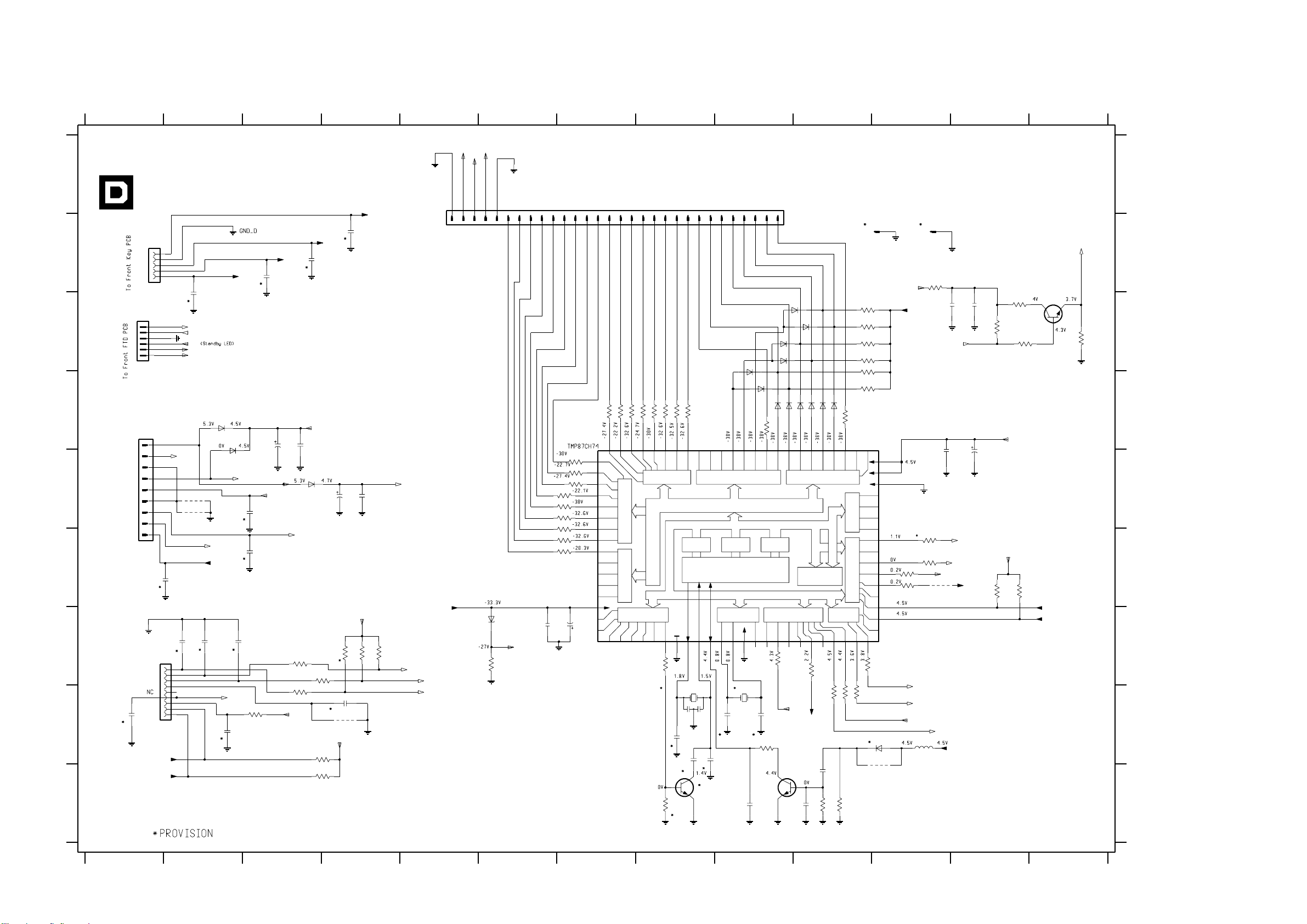
IR/FTD/LED BOARD - CIRCUIT DIAGRAM
6-5
6-5
A
B
C
D
123456789
+5VDSTBY
+5VL
56K
1K0
6200
BC857B
7201
3202
LTL-816EELC
SACD_LED
3204
12K
3218
10K
1K0
6201
3205
7202
BC847B
A
LTL-816TDK3
200
1
2
3
4
5
6
WH06D-1
+5VDSTBY
ioRC6
Standby_LED
+5VL
SACD_LED
7200
VS
OUT
GND
TSOP4836YA1
2200
100n
2201
3200
2202
1K0
4u7
2n2
3201
6202
10K
BZX384-C5V6
Standby_LED
3217
3203
12K
B
ioRC6
1202
FV818GN
P13
P14
P15
P16
P17
NC
8G
16
15
14
13
17
12
11
3G
4G
5G
6G
7G
6
7
8
9
10
F1
1G
2G
1
4
5
3214
22R
33R
3215
VGL-1
C
D
VGL-1
2203
33n
2204
+12VL
16V47u
3207
330R
+5VL
3209
47K
40kHZ
VGL+1
3212
22R
33R
3213
P2
P3
F2
32
P4
P1
P5
28
27
26
29
25
P10
P11
P6
P7
24
23
P12
P8
P9
20
19
18
22
21
200 A1
1201 E6
1202 B8
2200 A4
2201 A4
2202 B4
2203 D2
2204 D2
2205 E1
2206 D2
2207 D4
3200 A4
3201 A5
3202 A6
3203 A6
3204 A8
3205 A8
3206 D1
3207 D3
3208 D3
3209 D4
3210 D4
3211 E4
3212 C5
3213 D5
3214 C8
3215 D8
3216 D2
3217 A6
3218 B8
6200 A6
6201 A8
6202 B5
7200 A3
7201 A6
7202 A8
7203 D3
7204 E3
7205 D4
E
VGL+1
10u35V
2205
3206
470R
V_FIL
3216
470R
2206
35V10u
7203
BC817-25
7204
BC857B
3208
330R
7205
BC817-25
3210
3211
10K
10K
2207
22p
40kHZ
V_FIL
+12VL
E
30
29
28
27
26
25
24
23
22
21
20
19
1201
18
17
16
15
14
13
12
11
10
9
8
5
6
7
3
4
3139 113 35425_3139 113 3550 pt5_dd wk0428
1
2
123456789
Page 18

6-6 6-6
FRONT KEY BOARD - COMPONENT LAYOUT
This assembly drawing shows a summary of all possible versions. For components used in a specific version see schematic diagram and respective parts list.
FRONT KEY BOARD - CHIP LAYOUT
3139 113 3553 pt5 dd wk0428
This assembly drawing shows a summary of all possible versions. For components used in a specific version see schematic diagram and respective parts list.
3139 113 3553 pt5 dd wk0428
Page 19

6-7
6-7
FRONT KEY BOARD - CIRCUIT DIAGRAM
1300 A3
1301 C2
1302 B1
1303 B2
1304 B2
1305 B3
1306 B1
1307 A1
1308 A1
1309 A2
123
A
B
2301
GND_D
100p
3301
220R
1307
GND_D
3305 3303
390R
1308
GND_D
3300
150R
3304
270R
1310 C1
1311 D1
1309
GND_D
220R
2300 B1
2301 A1
3302
150R
3300 A2
3301 A1
GND_D
3302 B2
3303 B2
key1
key0
volA
3304 B2
3305 B1
FE-ST-VK-N
1300
5
4
3
2
volB
1
A
B
ELECTRICAL PARTS LIST - FRONT BOARD
MISCELLANEOUS
1100 4822 265 31205 FLEX CONNECTOR 5P
1102 2422 025 14518 FLEX CONNECTOR 9P
1103 2422 025 16586 FLEX CONNECTOR 9P
1103 2422 025 05587 FLEX CONNECTOR 9P
1107 2422 025 17411 FLEX CONNECTOR 30P
COILS & FILTERS
5100 4822 157 10586 FXD IND 2,2uH 10%
5102 2422 540 98518 RES CER 8MHz CSTS*MG03
DIODES
6100 4822 130 30621 1N4148
6101 4822 130 30621 1N4148
6102 4822 130 30621 1N4148
6104 4822 130 11148 BZX384-C4V7
6110 4822 130 11397 BAS316
6111 4822 130 11397 BAS316
6112 4822 130 11397 BAS316
6113 4822 130 11397 BAS316
6114 4822 130 11397 BAS316
6115 4822 130 11397 BAS316
6116 4822 130 11397 BAS316
6117 4822 130 11397 BAS316
6118 4822 130 11397 BAS316
6119 4822 130 11397 BAS316
6120 4822 130 11397 BAS316
6121 4822 130 11397 BAS316
TRANSISTORS & INTEGRATED CIRCUITS
7101 5322 130 60159 BC847B
7102 5322 130 60159 BC847B
7103 3139 240 50941 TMP87CM74AF - ‘LX8300S50941’
7104 5322 130 60159 BC847B
Note : Only the parts mentioned in this list are normal service
spare parts.
C
D
1304
3
B
C
GND_D
1
SRGP
A
245
1310
1
1311
1302
GND_D
SIN-01T-1.8
SIN-01T-1.81
100p
2300
GND_D GND_D
1306
GND_D
GND_D
GND_D
1303
GND_D
1301
1305
GND_D
3139 113 35425_3139 113 3553 pt5_dd wk0428
C
D
ELECTRICAL PARTS LIST - IR/FTD/LED BOARD
MISCELLANEOUS
1201 2422 025 17414 FLEX CONNECTOR 30P
1202 3139 111 04051 FTD FV818GN
DIODES
6200 9322 179 76676 LED VS LTL-816EELC
6201 9322 190 55676 LED VS LTL-816TDK3
6202 3198 020 55680 BZX384-C5V6
TRANSISTORS & INTEGRATED CIRCUITS
7200 9322 185 95667 IR RECEIVER TSOP4836YA1
ELECTRICAL PARTS LIST - FRONT KEY BOARD
7201 4822 130 60373 BC857B
7202 5322 130 60159 BC847B
7203 4822 130 42804 BC817-25
7204 4822 130 60373 BC857B
7205 4822 130 42804 BC817-25
Note : Only the parts mentioned in this list are normal service
spare parts.
123
MISCELLANEOUS
1300 4822 267 10958 FLEX CONNECTOR 5P
1301 2422 129 16936 ROT ENCODER 32P
1302 4822 276 13775 TACT SWITCH
1303 4822 276 13775 TACT SWITCH
1304 4822 276 13775 TACT SWITCH
1305 4822 276 13775 TACT SWITCH
1306 4822 276 13775 TACT SWITCH
1307 4822 276 13775 TACT SWITCH
1308 4822 276 13775 TACT SWITCH
1309 4822 276 13775 TACT SWITCH
Note : Only the parts mentioned in this list are normal service
spare parts.
Page 20

7-1 7-1
AV BOARD
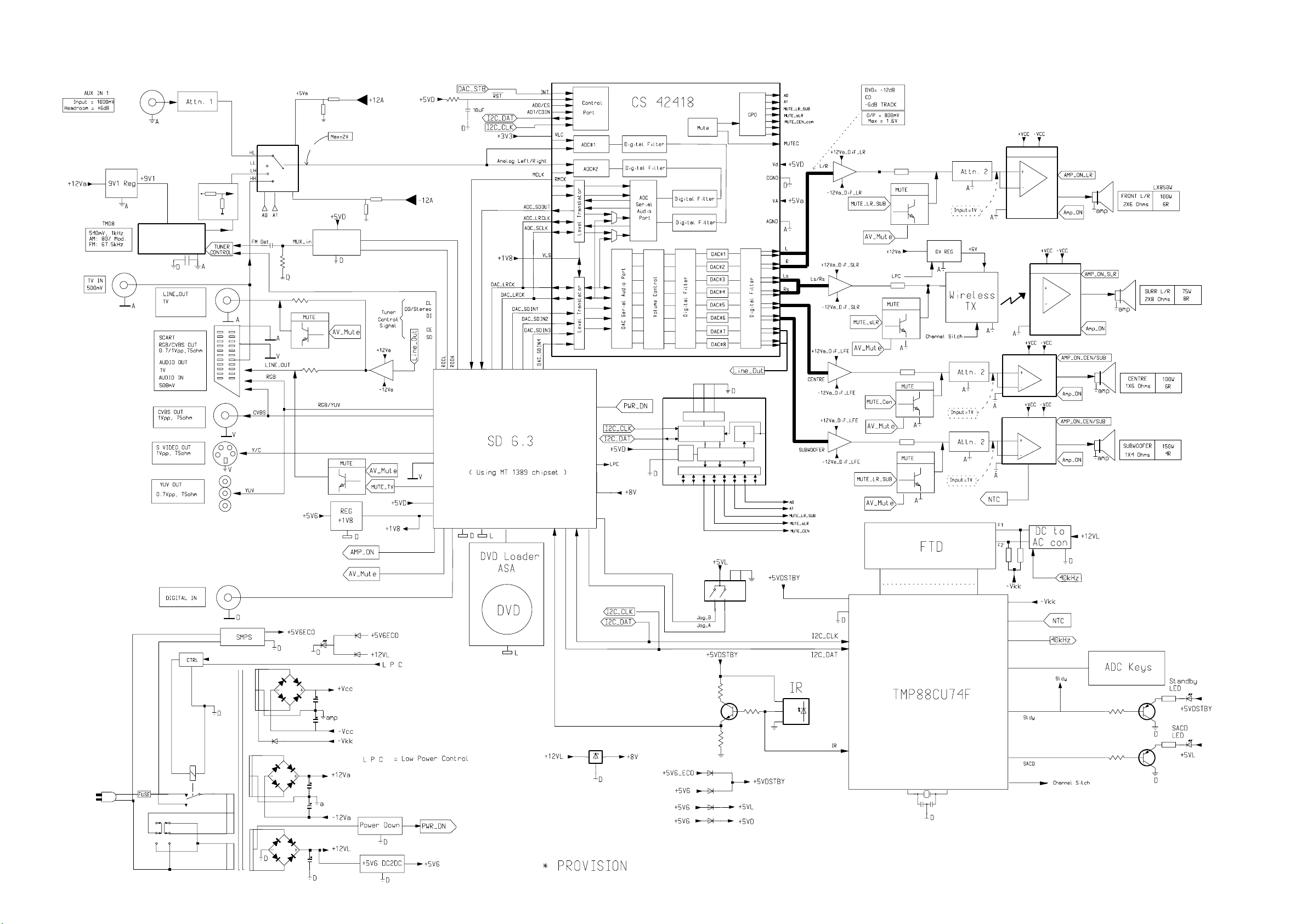
BRIEF INTRODUCTION OF THE AV BOARD
The AV Board consists of the following features :
a. IC CS42418
IC CS42418 acts as both DAC and ADC. It accepts PCM data at sample rate from 4kHz to 192kHz audio data. The analog
output is then fed into the Op-Amps which are used to filter and amplify the 6-channel signals before passing them onto the
Power-Amp module.
There are eight 24 bit DAC within this chip, 6 of those are dedicated to the 6-channel output, the other 2 are used for LINE
OUT signal.
This chip has 24 bit ADC. The internal stereo ADC is capable of independent gain control for single ended or differential
analog input. The digital output line ADC_SDOUT is then passed on to the MTK of the SD6.3 module. CS42418 is controlled
by the SD6.3 module via the I2C bus.
b.
IC HEF4052BT
The selection of TUNER, TV INPUT, AUX INPUT is made by IC HEF4052BT which acts as a multiplexer.
TABLE OF CONTENTS
Brief Introduction of the AV Board ................................... 7-1
Top View Layout .............................................................. 7-2
Bottom View Layout ......................................................... 7-3
Circuit Diagram (Part 1) ................................................... 7-4
Circuit Diagram (Part 2) ................................................... 7-5
Circuit Diagram (Part 3) ................................................... 7-6
Circuit Diagram (Part 4) ................................................... 7-7
Circuit Diagram (Part 5) ................................................... 7-8
Circuit Diagram (Part 6) ................................................... 7-9
Electrical parts list.......................................................... 7-10
c. Video signals are buffered (not for all versions) before connecting to the TV.
YUV OUT
d.
YUV OUT with cinch socket for connection to TV. Progressive Y Pb Pr is selected through RC.
e. LINE OUT
LINE OUT with cinch socket for connection to external amplifier.
f. SCART
SCART output for audio/video connection to TV (not for all versions).
g. S-Video and CVBS
S-Video and CVBS are used for video connection to the TV.
h. DIGITAL IN
DIGITAL IN with cinch socket for connection to DIGITAL OUT of other audio equipments.
The Digital_in source is fed to the SD6.3 module for audio decoding.
Page 21

AV BOARD - TOP VIEW LAYOUT
7-2
7-2
This assembly drawing shows a summary of all possible versions. For components used in a specific version see schematic diagram and respective parts list.
3139 113 3552 pt7 dd wk0428
Page 22

AV BOARD - BOTTOM VIEW LAYOUT
7-3
7-3
This assembly drawing shows a summary of all possible versions. For components used in a specific version see schematic diagram and respective parts list.
3139 113 3552 pt7 dd wk0428
Page 23

AV BOARD - CIRCUIT DIAGRAM (PART 1)
7-4 7-4
A
B
C
D
E
G
H
A
B
C
D
E
G
H
1100 B2
1102 D1
1103 F2
2100 B10
2108 D6
2109 D6
2110 E8
2111 D2
2112 D2
2113 C4
2114 C4
2115 D4
2116 D4
2117 E5
2118 F4
2119 F4
2120 F5
2121 F4
2122 F4
2123 G8
2124 G8
2125 G10
2127 G8
2128 H8
2129 H9
2131 H5
2132 H10
2134 I8
2135 I8
2136 I9
2139 B3
2140 B5
2141 B6
2142 G3
2143 H3
2144 H5
2150 E12
2151 E12
2152 C6
3101 A5
3102 A5
3111 B5
3112 B6
3113 A10
3114 B10
3118 C9
3121 D9
3123 C3
3124 C3
3125 D2
3127 E9
3128 D2
3130 E9
3131 D5
3132 D5
3133 E4
3134 E5
3135 F5
3136 F4
3137 F5
3138 F5
3139 G9
3140 G10
3142 G7
3143 G9
3144 G9
3145 G4
3146 G4
F
3147 H9
3148 H9
3150 H5
3151 H8
3152 H9
3153 H4
3154 H4
3155 H6
3156 H9
3157 H10
3159 H7
3160 I9
3161 I9
3162 I9
3163 I9
3165 I8
3166 I9
3168 B3
3169 C9
3170 D9
3171 H6
4105 E2
4106 D12
4109 E13
4110 E13
4113 E11
4114 D11
4115 E12
4116 C6
6101 B3
6102 H6
7100 B3
7101 G4
7102 H4
7103 G5
I
7104-A G8
7104-B H8
7105 B8
12345678910111213
Tu_CLK
1
TU_DO_STEREO
2
TU_Dat_In
3
4
TU_CE
5
6
TU_RDS_IN
7
8
Tu_SD
9
10
1
3
2
GND_sel
11
1100
GND_sel
4105
1103
LPR6520-J440G
2111
GND_a
3125
3K3
3128
3K3
68p
68p
2112
GND_sel
D
3
1
2
6
4
5
GND_sel
GND_a
FE-BT-VK-N
1102
LPR6520-J920G
GND_sel
F
7100
BC368
6101
BZX384-C10
GND_a
3K3
3123
GND_a
3168
2139
GND_a
3124
2142
2143
3K3
150R
100u 25V
GND_sel
100p
3145
3153
100p
2113
+12VA
SCART_TV_Left_In
SCART_TV_Right_In
68p
68p
2114
GND_sel
2115
100p
GND_sel
GND_sel
3133
3K3
68p
2118
2119
GND_sel
3136
3K3
68p
7102
7101
2122
GND_sel
3146
1K5
3154
1K5
2121
GND_sel
BC847B
47K
BC847B
47K
I
1234
100p
2116
3134
100p
GND_sel
3137
100p
7103
BC857B
3102
560R
2100
6K8
3114
GND_sel
3113
5K6
Right_In
Left_In
+12A
4114
V1
4113
V
4106
2150
100n
4115
2151
100n
D
GND_a
GND_sel
4110
4109
GND_LR
3101
560R
3131
GND_sel
3135
3111
GND_sel
470K
GND_sel
2117
1u0
68K
150K
GND_sel
3132
2140
D
470K
100p
GND_sel
2152
100n
2108
1u0
2109
1u0
3112
150K
2141
100p
GND_sel
4116
GND_a GND_sel
9
16
VDD
7105
HEF4052BT
LL
1
5
LH
HL
23
4
HH
12
LL
LH
14
15
HL
HH
11
VSS
8
GND_sel
7
VEE
2110
10
LOGIC
6
16V 1u0
LSBMSB
H
L
H
13
L
3127
10K
6K8
3130
GND_selGND_sel
Source_sel_A1
Source_sel_A0
3118
GND_sel
3121
GND_sel
16V1u0
GND_sel
3169
100R
470K
3170
100R
470K
-12A
GND_sel
2120
1u0
1
-12Va_LO
LM833D
7
7104-B
+12Va_LO
100n
2123
4
2127
100n
2128
82p
3151
12K
+12Va_LO
8
4
-12Va_LO
2135
82p
3165
12K
7104-A
LM833D
82p
GND_a
82p
GND_a
2124
2134
3139
3147
3152
3156
3162
3166
15K
3143
12K
15K
2129
8K2
470p
15K
3160
12K
15K
2136
8K2
470p
3144
8K2
3148
10K
3161
8K2
3163
10K
GND_a
8
3
2
5
6
470p
GND_a
470p
2125
2132
3140
10K
3157
10K
LO_Right_-
GND_a
LO_Right_+
LO_Left_-
GND_a
LO_Left_+
AV Circuit1_3139 113 35437_3139 113 3552 pt7_dd wk0428
GND_sel
2131
D
3138
6.3V
4u7
68K
2144
3150
GND_a
3142
LINE_R
+5VA_MUTE_LO
47K
3155
82K
6.3V4u7
3171
AV_Mute
6102
82K
BAS316
D
LINE_L
4K7
GND_a
MUTE_FRONT
3159
4K7
5678910111213
Page 24

AV BOARD - CIRCUIT DIAGRAM (PART 2)
1 2 3 4 5 6 7 8 9 10 11 12 13 14
A
B
+3V3
SCL_DAC
SDA_DAC
5220
2205
1u0
2206
D
D
C
1200
1
D
2
3
4
100p
5
6
7
8
9
10
11
12
13
14
15
16
17
18
19
20
21
22
23
24
25
26
27
28
29
30
D
E
F
2239
D
G
H
D
D
D
D
D
D
GND_a
GND_dig
3230
D
PCM_Data_LR
PCM_Data_SLR
PCM_Data_Sub_Cen
2227
D
470n
SCL_DAC
SDA_DAC
Tu_SD
TU_CE
TU_Dat_In
TU_DO_STEREO
TU_CLK
DIG_IN
AMP_ON
PWR_DN
Wireless_Mute
1K0
1K0
3268
3284
10K
4200
32701K0
100p
2250
D
I
12345678
100n
3280
3244
+5VD
ERR
+3V3
NTC
D
2K2
47K
2251
PCM_Data_Sub_Cen
PCM_Data_SLR
PCM_Data_LR
2K2
3245
Right_In
25V47u
D
3287
47K
3281
100p
D
D
PCMDATA_LO
D
Left_In
D
2222
3286
100K
47K
PCM_Data_Mic_In
+3V3
3285
D
2240
D
2u2
7-5
+5VD
47K
BC857B
7210
2218
10u
2221
2224
2229
10u
D
D
PCMCLK
5221
50V
1u0
1u0
50V
6206
BAS316
2238
10 SYNC
+5VD
3251
2220
D
2225
100n
3 VREF
RDCL16
RDDA2
QUAL1
+5VA
3252
100K
470p
3258
470p
MUTE_TV
12
POW SUPPL
RDS/RBDS
SIGNAL
QUALITY
VSSD
11
D
3235
+5VD
100K
100K
5
&
RESET
DEM
DET
VSSA
6
D
3272
2254
33R
3253
VDDAVDDD
D
D
14
2K2
3294
33R
3242
33R
100K
VSSA
47p
3293
33R
+5VA
3254
3259
OSC
CLK
3271
220K
4M332
5231
AT-51
33R
3234
3295 33R
100K
+3V3
+5VD
100K
D
57 Khz
BANDPASS
(8th ORDER)
CLOCKED
&
OSCI13OSCO
12
2255
D
3243
33R
3260
3264
COMP
TEST
CTRL
82p
+5VA
100K
100K
2217
D
3255
3261
100K
3283
100R
7201
SAA6581T
MPX 4
SCOUT 8
CIN 7
MODE 9
1u0
10K
+5VD
D
3262
7-5
1200 C1
3292 G13
2200 A10
3293 B5
3294 B5
2201 A9
3295 A5
2202 A10
3296 A7
2205 B2
4200 F2
2206 B3
2207 F13
5216 A10
5217 A10
2208 A9
5220 B2
2210 B6
5221 B4
2211 C12
5222 C13
2212 C12
A
B
C
D
E
F
G
H
I
2213 C11
2216 C11
2217 C6
2218 D4
2220 D4
2221 D4
2222 E3
2224 E4
2225 E4
2226 E8
2227 D2
2229 E4
2230 E6
2231 E6
2234 E7
2237 E7
2238 G4
2239 F1
2240 G4
2241 G6
2242 G7
2243 F12
2245 G6
2246 F12
2247 G6
2250 H2
2251 H3
2252 H9
2254 I5
2255 I5
2257 H9
2258 G12
2259 H13
2260 G12
3210 G8
3211 G8
3212 G9
3213 G9
3214 I9
3215 I9
3220 I8
3221 I8
3222 H10
3223 I10
3224 I10
3225 G9
3226 G9
3227 G9
3228 H9
3229 I10
3230 H2
3233 A6
3234 A5
3235 A5
3236 A6
3237 A7
3238 A7
3239 A6
3241 B6
3242 B5
3243 B5
3244 B3
3245 B3
3246 C12
3247 C6
3248 C12
3249 C6
3250 C6
3251 C4
3252 C4
3253 C5
3254 C5
3255 C6
3258 D4
3259 D5
3260 D5
3261 D5
3262 D6
3263 D6
3264 E5
3265 E6
3268 G2
3269 G6
3270 G2
3271 H5
3272 I5
3273 B10
3274 B10
3275 B10
3276 B10
3277 B10
3278 C10
3279 C10
3280 H3
3281 H3
3282 F12
3283 F6
3284 F2
3285 F4
3286 F4
3287 G3
5223 E8
5231 I5
6201 F12
6202 F13
6203 B13
6204 B13
6205 C13
6206 F4
6208 G12
6209 G13
6210 H13
7200 C8
7201 G6
7202 F12
7210 F4
7213 G13
+5VA
100K
2210
100n
3247
3233
33R
3296 33R
3236
33R
3239
33R
3241
33R
D
33R
3249
33R
D
3250
10K
D
3263
100K
1
2
3
4
5
6
7
8
9
10
11
12
13
14
15
16
3238
33R
DAC_SDIN1
DAC_SCLK
DAC_LRCK
VD_1
DGND_1
VLC
SCL_CCLK
SDA_CDOUT
AD1_CDIN
AD0_CS_
INT
RST_
AINR-
AINR+
AINL+
AINL-
3237
33R
64
DAC_SDIN2
17VQ18
62
63
DAC_SDIN4
DAC_SDIN3
FILT+19REFGND
D
61
ADC_SCLK
AOUTB4-
20
60
21
58
59
OMCK
ADCIN1
ADC_LRCK
AOUTB4+
AOUTA4+23AOUTA4-24VA_125AGND_1
22
57
ADCIN2
7200
CS42418
56
ADC_SDOUT
2226
100n
53
54
55
VLS
NC_3
RMCK
AOUTB3-26AOUTB3+27AOUTA3+
28
D
52
DGND_2
AOUTA3-
29
50
51
49
NC_2
NC_1
VD_2
AOUTB2-30AOUTB2+31AOUTA2+
32
GPO1
GPO2
GPO3
GPO4
GPO5
GPO6
GPO7
AGND_2
LPFLT
MUTEC
AOUTA1-
AOUTA1+
AOUTB1+
AOUTB1-
AOUTA2-
48
47
46
45
44
43
42
41
VA_2
40
39
38
37
36
35
34
33
2201
2208
1u0
100n
D
1u0
100n
D
DAC_L_+
DAC_R_+
DAC_R_-
5216
+3V3
2200
D
5217
+3V3
2202
D
3273
1K0
3275
1K0
3277
1K0
3279
1K0
3274
1K0
3276
1K0
3278
1K0
Source_sel_A0
Source_sel_A1
AMP_ON_LR_SUB_com
AMP_ON_SLR_com
MUTE_LR_SUB_com
MUTE_SL_SR_com
MUTE_CEN_com
5222
6203
BAS316
6204
BAS316
6205
BAS316
MUTE_LR_SUB
MUTE_SL_SR
MUTE_CEN
+5VA
D
2213
Mutec
LO_Left_-
LO_Left_+
LO_Right_+
LO_Right_-
680p
2n2
2216
47u
2211
100n
3248
10K
3246
2212
10K
D
D
D
D
D
DAC_L_-
DAC_LS_-
100u
100u
3225
3226
3227
3228
22R
22R
22R
22R
DAC_LFE_-
3222
22R
3223
22R
3224
22R
3229
22R
DAC_LS_+
DAC_RS_+
DAC_RS_-
DAC_C_-
DAC_C_+
DAC_LFE_+
+12Va_LO
+12Va_Dif_SLR
+12Va_Dif_LR
+12Va_Dif_LFE
-12Va_Dif_SLR
-12Va_Dif_LR
-12Va_Dif_LFE
-12Va_LO
+12VA
+12VA
BAS316
6208
2260
D
7202
BC547B
1K2
3282
6201
BZX384-C5V6
470u 16V
10V100u
2243
2246
6202
BAS316
+5VA
1u0
2207
470u 10V
D
+5VA_MUTE
D
D
BC547B
2258
7213
1K5
3292
470u 16V
D
BZX384-C5V6
6210
BAS316
6209
2259
+5VA_MUTE_LO
100u 10V
D
AV Circuit2_3139 113 35437_3139 113 3552 pt7_dd wk0428
100K
2230
50V4u7
2231
100n
2234
100u
2237
100n
5223
3265
10V
+5VA
D
D
+5VD
560p
2241
47p
560p
2245
15TCON
D
2242
TU_RDS_IN
1n
10K
3269
2247
D
D
+12A
-12A
3210
3220
3211
22R
3221
22R
22R
3212
22R22R
GND_LR
3214
22R
3213
22R
2252
2257
3215
22R
9 1011121314
Page 25

AV BOARD - CIRCUIT DIAGRAM (PART 3)
G
7-6
7-6
A
B
C
D
E
F
G
H
2300 B2
2303 B4
2304 B3
2306 A4
2307 A4
2310 C2
2313 C4
2314 C3
2320 D2
2323 D4
2324 E3
2326 D4
2327 C4
2330 F2
2333 F4
2334 F3
2340 G2
2343 G4
2344 G3
2350 H2
2353 H4
2354 I3
2356 H4
2357 G4
2362 C7
2363 C8
2364 D10
2365 E10
2366 G10
2367 G10
2368 I7
2369 I7
2370 A10
2371 B10
2372 A11
2373 B11
2374 D11
2375 E11
2376 G11
2377 H11
3304 B4
3305 B3
3306 B3
3307 B3
3308 A8
3309 A9
3314 C4
3315 C3
3316 C3
3317 C3
3318 B8
3319 B9
3324 E4
3325 E3
3326 D3
3327 D3
3328 D8
3329 D9
3334 F4
3335 F3
3336 E3
3337 F3
3338 E8
3339 E9
3344 G4
3345 G3
3346 G3
3347 G3
3348 F8
3349 F9
3354 I4
3355 I3
3356 H3
3357 H3
3358 H8
3359 H9
3360 A10
3361 A10
3362 B10
3363 A8
3364 A9
3365 B8
3366 B9
3370 D10
3371 D10
3372 E10
3373 E10
3374 D8
3375 D9
3376 E8
3377 E9
3378 B10
3380 F10
3381 G10
3382 H10
3383 G10
3384 G8
3385 G9
3386 G8
3387 G9
3390 C7
3391 C7
3392 C7
I
3393 D7
3394 H7
3395 I7
3396 I7
3397 I7
7300-A A4
7300-B B4
123456789101112
+12Va_Dif_LR
A
GND_LR
DAC_L_-
2300
1u0
B
C
DAC_L_+
2310
1u0
GND_LR
3307
10K
3n3
2304
3317
10K
3n3
2314
3306
3305
18K
3316
1K0
3315
18K
1K0
GND_LR
3
2
-12Va_Dif_LR
+12Va_Dif_LR
5
6
-12Va_Dif_LR
+12Va_Dif_LR
3
2
-12Va_Dif_LR
+12Va_Dif_LR
5
6
-12Va_Dif_LR
3326
3325
18K
GND_LR
1K0
D
DAC_R_-
2320
1u0
GND_LR
3327
2324
10K
3n3
E
GND_LR
DAC_R_+
2330
3337
1u0
GND_LR
2334
3336
1K0
10K
3n3
3335
18K
7300-A
LM833D
7300-B
LM833D
7301-A
LM833D
7301-B
LM833D
2307
100n
8
GND_LR
1
4
2306
100n
GND_LR
2303
220p
3304
3K3
8
7
7303
3390
47K
3391
82K
3392
82K
3393
82K
BC857B
4
2313
220p
3314
3K3
2327
100n
8
GND_LR
1
4
2326
100n
GND_LR
2323
220p
3324
3K3
8
7
4
2333
220p
3334
3K3
+5VA_MUTE
AV_Mute
MUTE_LR_SUB
Mutec
GND_LR
1u0
D
GND_LR
Sub_Mute
4u7
2362
D
3308
1K0
3318
1K0
2363
3328
1K0
3338
1K0
7306
BC847B
BC847B
7307
7310
BC847B
BC847B
7311
Sub_Mute
Sub_Mute
3363
3365
3374
3376
3309
1K0
3364
1K0
1K0
1K0
1K0
1K0
3366
1K0
3319
1K0
3329
1K0
3375
1K0
3377
1K0
3339
1K0
BC847B
7308
7309
BC847B
BC847B
7312
7313
BC847B
2370
2371
2364
2365
100p
100p
100p
100p
3361
22K
3371
22K
3360
100R
22K
3362
3378
100R
3370
100R
22K
3373
3372
100R
GND_LR
GND_LR
2372
2373
2374
2375
Amp_Left_-
330p
GND_aGND_LR
330p
Amp_Left_+
Amp_Right_-
330p
GND_a
330p
Amp_Right_+
F
+12Va_Dif_LFE
5
8
7302-B
GND_LR
DAC_C_-
2340
1u0
GND_LR
3347
2344
H
DAC_C_+
2350
1u0
GND_LR
3357
2354
3346
3345
18K
1K0
+12Va_Dif_LFE
8K2
3n3
GND_LR
3356
8K2
3n3
3355
18K
1K0
LM833D
6
-12Va_Dif_LFE
3
7302-A
LM833D
2
-12Va_Dif_LFE
I
7
4
2343
220p
3344
3K3
2357
100n
8
GND_LR
1
3394
47K
3395
82K
3396
82K
3397
82K
7305
BC857B
4
2356
100n
GND_LR
2353
220p
3354
3K3
+5VA_MUTE
AV_Mute
MUTE_CEN
Mutec
2369
D
GND_LR
1u0
2368
D
3348
3358
C_Mute
1K0
BC847B
BC847B
1K0
4u7
7322
7323
3384
1K0
C_Mute
3386
1K0
3349
3385
3387
3359
3380
1K0
BC847B
1K0
7324
2366
100p
3381
100R
22K
Amp_Center_-
2376
GND_LR
7325
2367
1K0
1K0
BC847B
100p
22K
3383
3382
100R
2377
GND_a
330p 330p
Amp_Center_+
AV Circuit3_3139 113 35437_3139 113 3552 pt7_dd wk0428
7301-A D4
7301-B E4
7302-A H4
7302-B G4
7303 C7
7305 H7
7306 A8
7307 B8
7308 A9
7309 B9
7310 D8
7311 E8
7312 D9
7313 E9
7322 G8
7323 G8
7324 G9
7325 G9
123456789101112
Page 26

AV BOARD - CIRCUIT DIAGRAM (PART 4)
7-7 7-7
1234567891011
56R
BC857B
75R
7423
BC847B
V
47p
7422
5406
5407
SCART_TV_Right_In
GND_a
SCART_TV_Left_In
+12VL
3420
V
3445
7421
BC847B
B_S
2415
470R
470R
SCART0
SCART1
+5V
3426
+5V
10K
10K
3427
7418
BC847B
3428
10K
2433
10u 50V
V
3467
10K
V
150R
3432
150R
3433
150R
3430
150R
3431
BC857B
7401
V1
BC857B
V1
7400
G
47p
2477
3462
2493
150R
V1
B_S
47p
75R
3435
2478
V1
V1
3434
1u8
4416
5404
+5V
390R
+5V
V1
4413
V1
220p
6407
CVBS_S
5409
BZX384-C15
V1
G_S
5408
2432
LINE_L
150R
3472
150R
3471
2413
2476
3410
82K
3461
3401
4u7
D
BC857B
7425
V
47p
47p
V1
2472
150R
3481
150R
3482
3439
2475
BC857B
47K
2u2
2411
75R
3438
V1
A
B
V
C
D
E
F
LPR6520-K410G
G
1411
1401
V1
1
2
GND_dig
1
2
3
4
5
6
7
8
9
10
11
12
13
14
15
16
17
18
19
20
21
22
23
24
25
26
27
28
29
30
4408
4405
3498
150R
SCART0
2410
100n
3499
GND_a
D
V
V
CVBS_DVD
V1
V1
2409
100n
D
D
D
D
D
150R
GND_dig
2470
P50
D2_Line2
SCART1
SY
SC
PCMDATA_LO
2408
100p
D
PCM_Data_Mic_In
Mic_det
2469
10n
180p
MUTE_TV
MUTE_FRONT
AV_Mute
3422
100K
3421
+5VD
47K
BC857B
7426
6401
BAS316
AV_Mute
D
3423
47K
3404
82K
6410
BAS316
LINE_R
3408
2471
82K
4u7
D
47p
47p
3411
2484
2490
150R
1u8
4417
75R
V
BC857B
V1
7404
3477
R
5405
+5V
390R
+5V
V
4410
47p
2492
150R
V1
R_S
V1
2485
V
47p
3473
D
V
PCMCLK
33p
2407
D
DIG_IN
2473
47p
2491
150R
3460
47p
2474
V1
1u8
4414
5402
+5V
47p
75R
3446
3447
390R
+5V
V1
V1
V1
4411
150R
3444
150R
3450
150R
3442
150R
3443
BC857B
7405
V1
+5VA_MUTE_LO
3400
4K7
7416
3402
2K2
3405
2K2
4u7
BC847B
1n
1n
BC847B
2404
2406
7417
7411
3403
3406
47K
2402
100p
GND_a
47K
2412
100p
D
3407
4K7
+5V
CVBS_S
47K
3469
150R
3436
150R
3437
BC857B
7403
V1
3474
3478
3468
12K
3475
22K
BC857B
7402
V1
B
4415
BC857B
V
390R
7420
CVBS
5403
1u8
+5V
4412
+5V
150R
3440
150R
3441
For scart version include all except for 4410, 4411, 4412, 4413
For non-scart version include only 4410, 4411, 4412, 4413
H
+5VD
I
4401
2429
+5V
47u
2430
47u
V1
V
4409
D
GND_a
SY
47p
47p
3451
2494
24802482
SC
2495
V
47p
47p
3456
V
12345
6 7 8 9 10 11 12 13 14
150R
150R
5400
5401
1u8
4418
1u8
4419
2481
2483
47p
12K
3452
3453
150R
V
47p
12K
3455
3454
150R
V
CVBS
12 13 14
For Scart version only
SCART 1
1400
V1
V1
G_S
V1
R_S
V
22n
220p
2431
V
V
V
R
B
4406
2461
470u10V
2462
10V 470u
4407
1
2
3
4
5
6
7
8
9
10
11
12
13
14
15
16
17
18
19
20
21
G
2457
16V
4404
S-VIDEO
220p
2465
V
2496
220p
V
2419
2420
220p
2421
220p
220p
2423
V
100n
2422
220p
6406
BZX384-C22
2416
220p
6408
BZX384-C15
2424
100n
6409
BZX384-C15
2418
220p
6417
BZX384-C15
2427
220p
V1
V1
1402
1403
YUV/
PROG SCAN
4402
2459
470u16V
4403
2458
16V 470u
470u
2455
2454
100p
V1
1
2
V
3
4
220p
2467
V
V
AV Circuit4_3139 113 35437_3139 113 3552 pt7_dd wk0428
Pin 8
0 - 2V :
4.5 - 7V :
9.5-12V :
Pin 16
0 - 0.4V :
1 - 3.0V :
V
100p
2456
V1
100p
V1
LAP5100-1301G
5
1409-B
78
LAP5100-1301G
TV BCAST
16 : 9 DVD
4: 3 DVD
V
V
LPR6520-N520F
V1
LPR6520-N620F
V
CVBS
CVBS
EXT RGB
1407
1
2
1408
1
3
2
V1
1409-A
6
1400 A12
1401 A2
1402 D13
1403 E13
1407 F14
1408 F14
1409-A H14
1409-B I14
1411 F1
2402 A8
2404 A8
2406 A8
2407 E3
A
2408 E2
2409 C2
2410 B2
2411 B7
2412 B8
2413 B6
2415 B11
2416 C13
2418 D13
2419 A13
2420 A13
2421 B13
B
2422 B13
2423 B13
2424 C13
2427 D13
2429 H2
2430 H3
2431 D12
2432 D11
2433 C10
2454 G13
2455 G13
C
2456 F13
2457 G12
2458 G13
2459 F13
2461 H12
2462 I12
2465 H12
2467 H13
2469 F3
2470 F2
2471 B6
2472 B7
D
2473 F4
2474 F4
2475 F7
2476 F6
2477 E9
2478 F9
2480 H9
2481 H11
2482 I9
2483 I11
2484 C5
2485 D5
E
2490 C5
2491 E4
2492 F6
2493 E9
2494 H9
2495 I9
2496 I12
3400 A7
3401 A7
3402 A7
3403 A8
F
3404 A6
3405 B7
3406 B8
3407 B7
3408 A6
3410 A7
3411 C5
3420 C10
3421 B4
3422 B4
3423 B3
3426 B9
G
3427 B9
3428 C10
3430 F10
3431 F10
3432 F10
3433 F10
3434 F9
3435 F9
3436 F8
3437 F8
3438 F7
3439 F7
H
3440 F8
3441 F8
3442 F5
3443 F5
3444 F5
3445 C10
3446 F4
3447 F4
3450 G5
3451 H10
3452 H11
I
3453 H11
3454 I11
3455 I11
3456 I10
3460 E4
3461 F6
3462 E9
3467 D10
3468 C8
3469 C9
3471 D6
3472 D6
3473 D5
3474 D8
3475 D9
3477 D6
3478 D8
3481 C7
3482 C7
3498 F2
3499 F2
4401 H2
4402 F13
4403 F13
4404 G12
4405 F2
4406 H12
4407 I12
4408 G2
4409 I8
4410 E6
4411 H5
4412 G7
4413 G10
4414 F4
4415 F7
4416 F9
4417 C6
4418 H10
4419 I10
5400 H10
5401 I10
5402 F4
5403 F7
5404 F10
5405 C6
5406 A9
5407 A9
5408 A11
5409 B11
6401 B4
6406 B13
6407 B11
6408 C13
6409 C13
6410 A6
6417 D13
7400 F11
7401 G10
7402 F8
7403 G8
7404 F6
7405 G5
7411 A8
7416 A7
7417 A8
7418 C10
7420 D7
7421 D11
7422 D9
7423 D9
7425 D7
7426 B4
Page 27

AV BOARD - CIRCUIT DIAGRAM (PART 5)
7-8 7-8
A
B
C
D
G
H
A
B
C
D
E
F
G
H
1507 A13
1509 A1
1511 E12
2503 B10
2504 B11
2505 B11
2506 B11
2507 C3
2508 C4
2509 C3
2510 D2
2511 C4
2512 E6
2513 D6
2514 D6
2515 A5
2516 A6
2517 E4
2518 E5
2519 B5
2520 B6
2521 G5
2522 G5
2523 G5
2524 G6
2525 G6
2526 A4
2527 C3
2528 D3
2529 D2
2530 G8
2531 G9
2532 E9
2533 E8
2534 E1
2535 G2
3502 A2
3503 A2
3504 C9
3505 B10
3506 A2
3507 A2
3508 D5
3509 D5
3512 C10
3522 F11
3523 C3
3524 D7
3525 E7
3526 E7
3527 E2
3528 G2
3540 G7
3541 G7
3542 G8
3543 G9
3544 G9
3545 E10
3546 E10
3547 E9
3548 E8
3549 E8
3550 E8
3551 C9
3552 D10
4506 A5
4507 H2
4508 F8
5505 C4
5507 C7
6505 B5
6506 A5
6507 G8
6508 F2
6509 F2
6510 F2
7501 A6
7502 C5
7503 D6
7504 D6
7505 G6
7506 C11
7508 A5
7509 C10
7512-A G9
7512-B E9
7513 C9
12345678910111213
330p
+12VL
2517
2511
6506
S1D
4506
16V
220u
D
3509
68R
50V10u
2521
2515
100n
6505
SS24
2522
100n
2519
3508
22R
2518
220u 16V
7508
LD1117
3
IN2OUT
100n
BCP53
100n
IN
2523
GND
1
+5VD
+5V6
7502
3
L7808CD2T
GND
100n
1
7505
COM
D
7503
BC847B
OUTIN
D
7501
LD1117
IN3OUT
GND
1
2513
2
7504 TS431L
R4
NC
12
OUT
2524
+3V3D
100u
2516
+5V6
2
2520
100u
+3V3
D
+5VD
3505
10K
15K
3551
5507
2514
100MHZ
100n
50V10u
1V8B
AMP_ON
3504
22K
7513
BC847B
3512
D
7509
BC847B
D
D
A
5
K3
D
2512
100n
D
5K6
3524
Vref
3525
D
10K
3526
220K
PWR_DN_AMP
3549
470K
2533
Vref
22K
3548
3550
6K8
3547
47n
D
5
8
6
18K
100n
2532
7512-B
4
LM833D
3552
3545
7
10K
+12VL
D
+5V6_ECO
2506
100n
2505
100n
100n
2504
D
22u50V
D
2503
4K7
D
BC857B
7506
D
Amp_On_LR_CS
Ch_Sw
D
MUTE_FRONT
-VKK
NTC
D
10K
PWR_DN_W
D
3546
PWR_DN
22K
+8V
1V8B
D
D
+5VD
+5VD
D
+8V
D
DAC_STB
VSCK
VSDA
D
100n
2525
25V
100u
3522
1K0
+5V6
4508
BAS316
6507
Vref
100u10V
2531
Power_ON
D
3
22K
+8V
Vref
3540
3541
NTC
3K9
18K
2530
3542
100n
D
8
3543
1
2
4
7512-A
LM833D
10K
3544
ERR
22K
D
FE-BT-VK-N
1507
1
2
3
4
5
6
7
8
9
1511
1
2
3
4
5
6
7
8
9
10
11
12
13
14
15
16
FMN
D
GND_a
3506
22R
3507
22R
GND_a
GND_a
2510
6510
BAS316
6509
BAS316
6508
BAS316
+12VA
-12VA
1509
1
2
3
4
5
6
7
8
9
10
11
12
13
14
15
16
17
18
19
20
21
22
23
24
25
26
27
28
29
30
31
32
33
34
35
36
38
37
N10236-52B2VC
2534
330p
E
F
D
PWR_DN_W
Amp_On_LR_CS
MUTE_SL_SR_com
Amp_Left_+
Amp_Left_Amp_Right_+
Amp_Right_-
Amp_Center_+
Amp_Center_-
Amp_Lfe_+
Amp_Lfe_-
Power_ON
Amp_Surr_Left_+
Amp_Surr_Left_Amp_Surr_Right_+
Amp_Surr_Right_-
Wireless_Mute_Amp
D
2529
100u 25V
D
D
+5V6
3527
3528
3502
22R
3503
22R
-VKK
Amp_On_LR_CS
+12VL
Ch_Sw
PWR_DN_AMP
+5V6_ECO
330p
33K
39K
2535
10V220u
2527
D
+12A
-12A
330p
2509
2507
220u 16V
GND_a
D
+5VD
10K
3523
2528
330p
D
Wireless_Mute_Amp
NTC
+5V6
2526
D
-12VA
+12VA
+5V6
100u
2508
25V
100u 25V
GND_a
+3V3D
5505
100MHZ
D
Wireless_Mute
4507
12345
AV Circuit5_3139 113 35437_3139 113 3552 pt7_dd wk0428
6 7 8 9 10 11 12 13
Page 28

AV BOARD - CIRCUIT DIAGRAM (PART 6)
7-9 7-9
G
A
B
C
D
E
F
G
H
2600 A5
2601 A2
2605 A5
2606 A10
2608 A5
2610 A3
2611 B10
2612 B2
2617 B5
2619 C3
2620 C5
2621 D2
2625 D5
2626 D10
2628 D5
2630 D3
2631 D10
2632 E2
2637 E5
2639 E3
2640 F7
2641 F7
2642 G2
2646 G10
2648 G5
2649 G2
2650 G3
2651 G10
2652 G5
2653 H2
2657 H5
2659 H5
2660 H2
2661 H3
2662 F2
2663 H2
2664 A11
2665 B11
2666 D11
2669 D11
2670 G11
2671 G11
3603 A8
3604 A9
3605 A10
3608 A8
3609 A9
3610 A3
3613 A3
3614 A3
3616 B8
3618 A10
3619 B10
3620 B9
3621 B9
3622 B8
3623 B10
3624 A5
3628 B3
3629 B3
3630 C3
3631 C5
3635 C8
3636 C9
3637 C10
3640 D8
3641 D9
3642 D10
3644 D3
3645 D3
3646 D3
3647 D5
3648 D8
3649 D9
3650 D10
3654 E8
3655 E9
3656 E10
3660 E3
3661 E3
3662 E7
3663 E3
3664 E5
3665 F7
3666 F7
3667 F7
3671 F8
3672 F9
3673 F10
3676 G8
3677 G9
3678 G10
3680 G3
3681 G3
3682 G3
3683 G5
3684 G8
3685 G9
3686 G10
3690 H8
3691 H9
3692 H10
3696 H3
3697 H3
3698 H3
3699 H5
123456789101112
+12Va_Dif_SLR
3
2
-12Va_Dif_SLR
+12Va_Dif_SLR
5
6
-12Va_Dif_SLR
+12Va_Dif_SLR
3
2
-12Va_Dif_SLR
+12Va_Dif_SLR
5
6
-12Va_Dif_SLR
+12Va_Dif_LFE
3
2
-12Va_Dif_LFE
+12Va_Dif_LFE
5
6
-12Va_Dif_LFE
3613
3614
3629
3630
GND_LR
1K0
18K
GND_LR
1K0
18K
A
DAC_LS_+
2601
1u0
GND_LR
3610
6K8
2610
3n3
B
DAC_LS_-
2612
1u0
GND_LR
3628
6K8
2619
3n3
C
GND_LR
D
DAC_RS_-
2621
1u0
GND_LR
3644
6K8
2630
3n3
3645
3646
1K0
18K
GND_LR
E
DAC_RS_+
2632
1u0
GND_LR
2639
3660
6K8
3n3
3661
3663
1K0
18K
F
3681
220K
3682
220K
3697
220K
3698
220K
GND_LR
GND_LR
2662
1u0
DAC_LFE_-
H
DAC_LFE_+
2642
2663
2653
1u0
1u0
1u0
330p
2649
330p
2660
GND_LR
GND_LR
3680
150K
2650
3696
150K
2661
6n8
6n8
7600-A
LM833D
7600-B
LM833D
7618-A
LM833D
7618-B
LM833D
7619-A
LM833D
7619-B
LM833D
2600
100n
2605
100n
220p
3624
3K3
2617
220p
3631
3K3
2620
100n
2625
100n
220p
3647
3K3
2637
220p
3664
3K3
2648
330p
3683
680K
2652
100n
2657
100n
2659
330p
3699
680K
1
2608
7
1
2628
7
1
7
GND_LR
GND_LR
GND_LR
GND_LR
GND_LR
GND_LR
+5VA_MUTE
AV_Mute
MUTE_SL_SR
Mutec
3662
3665
3666
3667
3603
1K0
7601
BC847B
GND_LR
BC847B
7603
3622
1K0
3635
1K0
7607
BC847B
GND_LR
BC847B
7609
3654
Surr_Mute
2641
1K0
4u7
3671
1K0
7614
BC847B
7612
BC857B
47K
82K
1u0
2640
82K
D
D
82K
GND_LR
BC847B
7616
3690
1K0
3608
1K0
Surr_Mute
3616
1K0
3640
1K0
Surr_Mute
3648
1K0
3676
1K0
Sub_Mute
3684
1K0
3604
1K0
3609
1K0
3621
1K0
3620
1K0
3636
1K0
3641
1K0
3649
1K0
3655
1K0
3672
1K0
3677
1K0
3685
1K0
3691
1K0
BC847B
7602
7604
BC847B
BC847B
7608
7610
BC847B
BC847B
7615
7617
BC847B
2606
2611
2626
2631
2646
2651
100p
100p
100p
100p
100p
100p
3618
22K
3642
22K
3678
22K
3605
100R
22K
3619
3623
100R
3637
100R
22K
3650
3656
100R
3673
100R
22K
3686
3692
100R
GND_LR
GND_LR
GND_LR
2664
2665
2666
2669
2670
2671
Amp_Surr_Left_+
330p
GND_a
330p
Amp_Surr_Left_-
Amp_Surr_Right_-
330p
GND_a
330p
Amp_Surr_Right_+
Amp_Lfe_-
330p
GND_a
330p
Amp_Lfe_+
AV Circuit6_3139 113 35437_3139 113 3552 pt7_dd wk0428
8
4
8
4
8
4
8
4
8
4
8
4
7600-A A4
7600-B B4
7601 A8
7602 A9
7603 B8
7604 B9
7607 D8
7608 D9
7609 D8
7610 D9
7612 E7
7614 G8
7615 G9
7616 G8
7617 G9
7618-A C4
7618-B E4
7619-A F4
7619-B H4
123456789101112
Page 29

7-10
7-10
ELECTRICAL PARTS LIST - AV BOARD
MISCELLANEOUS
1100 4822 267 11039 Flex Connector 11P
1102 ^ 2422 026 04754 Socket Cinch 2P (TV in)
1103 2422 026 05462 Socket Cinch 4P (Aux-in/Line-out)
1200 2422 025 17433 Flex Connector 30P
1200 2422 025 17509 Flex Connector 30P
1400 * 2422 025 18315 Socket SCART 21P
1400 * 2422 025 12352 Socket SCART 21P
1401 2422 025 17433 Flex Connector 30P
1401 2422 025 17509 Flex Connector 30P
1402 * 3139 241 21102 EMC SPRING
1403 * 3139 241 21102 EMC SPRING
1407 2422 026 05531 Socket Cinch 1P (Pr)
1408 2422 026 05529 Socket Cinch 2P (Y/Pb)
1409 2422 033 00468 Socket 2P (Video/S-Video)
1411 2422 026 05427 Socket Cinch 1P (Digital In)
1507 2422 025 14518 Flex Connector 9P
1509 2422 025 05561 Socket MDR 36P
1509 2422 025 18466 Socket MDR 36P
1511 2422 025 16525 Flex Connector 16P
COILS & FILTERS
5216 2422 549 43062 FXD IND 0603 100MHz 600R
5217 2422 549 43062 FXD IND 0603 100MHz 600R
5220 2422 549 43062 FXD IND 0603 100MHz 600R
5221 2422 549 43062 FXD IND 0603 100MHz 600R
5222 2422 549 43062 FXD IND 0603 100MHz 600R
5223 2422 549 43062 FXD IND 0603 100MHz 600R
5231 * 4822 242 11033 RES XTL 4,332MHz
5400 3198 018 41880 FXD IND SM 1210 1U8 5%
5401 3198 018 41880 FXD IND SM 1210 1U8 5%
5402 3198 018 41880 FXD IND SM 1210 1U8 5%
5403 3198 018 41880 FXD IND SM 1210 1U8 5%
5404 3198 018 41880 FXD IND SM 1210 1U8 5%
5405 3198 018 41880 FXD IND SM 1210 1U8 5%
5406 * 3198 018 90050 FXD IND 0603 100MHz 1K
5407 * 3198 018 90050 FXD IND 0603 100MHz 1K
5408 * 3198 018 90050 FXD IND 0603 100MHz 1K
5409 * 3198 018 90050 FXD IND 0603 100MHz 1K
5505 4822 157 11717 IND FXD 1206 EMI 100MHz 50R
5507 4822 157 11717 IND FXD 1206 EMI 100MHz 50R
DIODES
6101 4822 130 11551 BZX384-C10
6201 3198 020 55680 BZX384-C5V6
6202 4822 130 11397 BAS316
6203 4822 130 11397 BAS316
6204 4822 130 11397 BAS316
6205 4822 130 11397 BAS316
6206 * 4822 130 11397 BAS316
6208 4822 130 11397 BAS316
6209 4822 130 11397 BAS316
6210 3198 020 55680 BZX384-C5V6
6401 4822 130 11397 BAS316
6406 * 9340 548 67115 BZX384-C22
6407 * 4822 130 11522 BZX384-C15
6408 * 4822 130 11522 BZX384-C15
6409 * 4822 130 11522 BZX384-C15
6417 * 4822 130 11522 BZX384-C15
6505 3198 010 10720 DIO REC SS24
6506 9322 128 69685 DIO REC SM S1D
6508 4822 130 11397 BAS316
6509 4822 130 11397 BAS316
TRANSISTORS & INTEGRATED CIRCUITS
7100 5322 130 44647 BC368
7101 5322 130 60159 BC847B
7102 5322 130 60159 BC847B
7103 4822 130 60373 BC857B
7104 4822 209 30095 LM833D
7105 5322 209 11102 HEF4052BT
7200 9322 203 36668 IC SM CS42418-CQ
7201 * 9352 686 05118 IC SM SAA6581T
7202 4822 130 40959 BC547B
7210 * 4822 130 60373 BC857B
7213 4822 130 40959 BC547B
7300 4822 209 30095 LM833D
7301 4822 209 30095 LM833D
7302 4822 209 30095 LM833D
7303 4822 130 60373 BC857B
7305 4822 130 60373 BC857B
7306 5322 130 60159 BC847B
7307 5322 130 60159 BC847B
7308 5322 130 60159 BC847B
7309 5322 130 60159 BC847B
7310 5322 130 60159 BC847B
7311 5322 130 60159 BC847B
7312 5322 130 60159 BC847B
7313 5322 130 60159 BC847B
7322 5322 130 60159 BC847B
7323 5322 130 60159 BC847B
7324 5322 130 60159 BC847B
7325 5322 130 60159 BC847B
7400 * 4822 130 60373 BC857B
7401 * 4822 130 60373 BC857B
7402 * 4822 130 60373 BC857B
7403 * 4822 130 60373 BC857B
7404 * 4822 130 60373 BC857B
7405 * 4822 130 60373 BC857B
7411 * 5322 130 60159 BC847B
7416 * 4822 130 60373 BC857B
7417 * 5322 130 60159 BC847B
7418 * 5322 130 60159 BC847B
7420 * 4822 130 60373 BC857B
7421 * 5322 130 60159 BC847B
ELECTRICAL PARTS LIST - AV BOARD
7422 * 4822 130 60373 BC857B
7423 * 5322 130 60159 BC847B
7425 * 4822 130 60373 BC857B
7426 4822 130 60373 BC857B
7501 4822 209 17398 LD1117DT33
7501 4822 209 17398 LD1117DT33
7502 5322 130 62804 BCP53
7503 5322 130 60159 BC847B
7504 9322 146 75685 IC SM TS431IL
7505 9322 199 24668 IC SM L7808CD2T
7506 4822 130 60373 BC857B
7508 4822 209 17398 LD1117DT33
7508 4822 209 17398 LD1117DT33
7509 5322 130 60159 BC847B
7512 4822 209 30095 LM833D
7513 5322 130 60159 BC847B
7600 4822 209 30095 LM833D
7601 5322 130 60159 BC847B
7602 5322 130 60159 BC847B
7603 5322 130 60159 BC847B
7604 5322 130 60159 BC847B
7607 5322 130 60159 BC847B
7608 5322 130 60159 BC847B
7609 5322 130 60159 BC847B
7610 5322 130 60159 BC847B
7612 4822 130 60373 BC857B
7614 5322 130 60159 BC847B
7615 5322 130 60159 BC847B
7616 5322 130 60159 BC847B
7617 5322 130 60159 BC847B
7618 4822 209 30095 LM833D
7619 4822 209 30095 LM833D
Note : Only the parts mentioned in this list are normal
service spare parts.
* For /01/04 versions only
^ For /69/93 versions only
Page 30

8-1 8-1
BOX SPK ASSY SW8500LX
(Subwoofer & Module PWR308 Wireless)
Mains pt5 / Reg pt6 / Amp UCD pt4 / Spk pt5 - 23 August 04
TECHNICAL REMARKS
TABLE OF CONTENTS
Box Spk Assy SW8500LX
Exploded View & parts list ............................................... 8-2
Module PWR308 Wireless
Exploded View & parts list ............................................... 8-3
Wiring Diagram ................................................................ 8-4
Regulator Board - Component Layout ............................ 8-5
Regulator Board - Chip Layout ........................................ 8-6
Regulator Board - Circuit Diagram .................................. 8-7
Amplifier UCD Board - Top View Layout ......................... 8-8
Amplifier UCD Board - Bottom View Layout ................... 8-9
Amplifier UCD Board - Circuit Diagram (Part 1) ........... 8-10
Amplifier UCD Board - Circuit Diagram (Part 2) ........... 8-11
Mains Board - Component Layout ................................ 8-12
Mains Board - Circuit Diagram ...................................... 8-13
Mains Socket Board - Component Layout .................... 8-14
Mains Socket Board - Circuit Diagram .......................... 8-14
Speaker Board - Component Layout............................. 8-14
Speaker Board - Circuit Diagram .................................. 8-14
Electrical parts list.......................................................... 8-15
Page 31

8-2
EXPLODED VIEW - BOX SPK ASSY SW8500LX
PARTS LIST - BOX SPK ASSY SW8500LX
3139 119 02511 BOX SPK ASSY SW8500LX/01 /01/04
3139 119 02491 BOX SPK ASSY SW8500LX/69 /69/93
9965 000 25359 WF 6.5" 150W 4R (16L80EHC3495)
9965 000 25360 TOP COVER
9965 000 25361 BACK PANEL
9965 000 25362 PORT TUBE
9965 000 25363 PLASTIC FOOT
9965 000 25364 RUBBER FOOT
9965 000 25365 LED 3 DIA RED ROUND
9965 000 25737 WIRELESS MODULE TX
Note : Only the parts mentioned in this list are normal service
spare parts.
8-2
(MODULE PWR308
WIRELESS)
Exploded View_dd wk0435
Page 32

8-3
EXPLODED VIEW - MODULE PWR308 WIRELESS
8-3
PARTS LIST - MODULE PWR308 WIRELESS
0007 3139 240 40061 SPACER - 8MM
1001 3139 118 57951 PCBAS MAINS & MAINS SOCKET /01/04
1001 3139 118 57961 PCBAS MAINS & MAINS SOCKET /69/93
1002 3139 118 57911 PCBAS REGULATOR
1003 3139 118 57971 PCBAS SPEAKER
1004 3139 118 57981 PCBAS AMPLIFIER UCD
1005 3139 118 57981 PCBAS AMPLIFIER UCD
1008 3139 110 34950 FFC FOIL 07P/120/07P AD
1010 3139 110 34950 FFC FOIL 07P/120/07P AD
1018 3139 118 33031
!
TRANSFORMER MAINS /69/93
1020 3139 118 33021
!
TRANSFORMER MAINS /01/04
1021 3139 258 70061 FAN KD1209PTS3
1022 3139 111 04281 36P CABLE ASSY
Note : Only the parts mentioned in this list are normal service spare
parts.
Exploded View PWR308_3139 117 10791_dd wk0419
Page 33

8-4
WIRING DIAGRAM - MODULE PWR308 WIRELESS
8-4
1301
DIPMATE
EH-B
EH-B
1
2
3
4
1302
1
2
3
1300
1
2
3
4
5
6
7
TO INTERFACE CABLE
8
REGULATOR
+SEC_AC
-SEC_AC
+AMP_AC
GND_AMP
-AMP_AC
OV_PRO
SEC_V
+12V_A
-12V_A
1
2
3
1304
EH-B
1305
1
2
3
4
5
6
7
8
9
10
11
EH-B
SURR_L_W
SUR_R_W
CH_SW
+6V
ID_SEL
LT
LT_REF
RT
RT_REF
AMP_ON
OV_PRO
FREQ_HOP
SUR_LT
SUR_LT_REF
SUR_RT
SUR_RT_REF
AMP_ON
OV_PRO
FREQ_HOP
CEN
CEN_REF
SW
SW_REF
AMP_ON
OV_PRO
FREQ_HOP
1312
1
2
3
4
5
6
7
8
9
FMN
GND_D
GND_D
1306
1
2
3
4
5
6
7
1308
1
2
3
4
5
6
7
1310
1
2
3
4
5
6
7
+VH
GND_AMP
-VH
NTC_1
FE-BT-VK-N
FE-BT-VK-N
FE-BT-VK-N
LEFT_REF
RIGHT_REF
TO WIRELESS MODULE
CENTER
SUB_REF
SURR_L
SURR_L_REF
SUR_R_REF
AMP_ON
FREQ_HOP
CH_SW
Surround AMP Front AMP Center Sub AMP
EH-B
DIPMATE
1315
1
2
3
3
4
4
5
5
6
6
7
7
8
9
9
10
10
DIPMATE
0302
0301
1
1
2
2
3
4
5
6
7
8
8
9
10
NTC_3NTC_2
1309
EH-B
LEFT
RIGHT
1
2
3
4
5
C_REF
SUB
6
7
8
9
10
SUR_R
+12VL
GND_D
+12VL
11
12
1311
EH-B
1
2
3
4
5
6
1103 220mm
1101 280mm
1015 280mm
1102 280mm
1008 120mm
1009 120mm
1010 120mm
Center
TO INTERFACE CABLE
LEFT
RIGHT
TO INTERFACE CABLE
SUR_LEFT
SUR_RIGHT
1504-A
1504-C
1504-B
1500-B
1500-A
1023 280mm
GND_A
1
+
2
-
5
+
6
-
3
+
4
-
3
+
4
-
1
+
2
-
4
1908
TO STBY LED
EH-B
1
NTC
2
3
4
5
6
7
8
9
10
+AC
GND_AMP
-AC
TO STBY LED
CHANNEL1_POS
CHANNEL1_POS
EH-B
CHANNEL1_NEG
1505
CHANNEL1_NEG
1
2
CHANNEL2_POS
LED
CHANNEL2_POS
CHANNEL2_NEG
CHANNEL2_NEG
CHANNEL1_POS
CHANNEL1_POS
CHANNEL1_NEG
CHANNEL1_NEG
CHANNEL2_POS
CHANNEL2_POS
CHANNEL2_NEG
CHANNEL2_NEG
CHANNEL1_POS
SPEAKER
CHANNEL1_POS
CHANNEL1_NEG
CHANNEL1_NEG
CHANNEL2_POS
CHANNEL2_POS
CHANNEL2_NEG
CHANNEL2_NEG
LED
-SUB
+SUB
3
1
2
EH-B
1502
STBYLEDSUP
1
2
GND_A
1702
EH-B
MAINS CONNECTOR
AMP_ON
RIGHT_REF
AMP_RIGHT
MAINS
ERROR_DETECT
FREQ/MODESELECT
FRONT
+SEC_A
-SEC_A
0708
DIPMATE
1
2
3
4
MAINS
1101 180mm
+VCC
GND_AMP
-VCC
+SEC_AC_1
-SEC_AC_1
NTC
GND_A
GND_A
10
1100
1
2
3
4
5
6
7
8
9
1710
1
2
3
GND_AMP
+5V6_ECO
+12V_A
-12V_A
EH-B
CHANNEL1GND
CHANNEL1GND
CHANNEL1
CHANNEL1
CHANNEL2
CHANNEL2
CHANNEL2GND
CHANNEL2GND
-VKK
NTC
GND_D
PW_DN
LPC
+12V_A
GND_A
-12V_A
1
2
3
EH-B
0705
DIPMATE
1110
1
2
3
4
5
6
7
8
1709
1
2
3
4
5
6
7
8
9
10
EH-B
EH-B
1901 120mm
1900 120mm
1951
1
2
TO INTERFACE CABLE
1950
1
2
FE-BT-VK-N
1201
1234567
LEFT_REF
AMP_LEFT
AMPLIFIER UCD 1
1012 280mm
1100
1
2
3
4
5
6
7
8
9
10
1100
1
2
3
4
5
6
7
8
9
10
EH-B
CHANNEL1GND
CHANNEL1GND
CHANNEL1
CHANNEL1
CHANNEL2
CHANNEL2
CHANNEL2GND
CHANNEL2GND
EH-B
CHANNEL1GND
CHANNEL1GND
CHANNEL1
CHANNEL1
CHANNEL2
CHANNEL2
CHANNEL2GND
CHANNEL2GND
1110
EH-B
1
2
3
4
5
6
7
8
1110
EH-B
1
2
3
4
5
6
7
8
1506
EH-S
1
+VCC
2
3
4
5
6
1016 180mm
GND_AMP
7
8
1501
EH-S
1
2
3
-VCC
NTC
1013 220mm
4
5
+VCC
6
7
8
EH-S
1503
1
1102 180mm
GND_AMP
2
3
4
5
6
7
8
-VCC
NTC
1014 140mm
Wiring Diagram Module PWR308_3139 117 10791_dd wk0430
FE-BT-VK-N
1201
1234567
AMP_ON
SURR_LEFT_REF
AMP_SURR_LEFT
SURR_RIGHT_REF
AMP_SURR_RIGHT
AMPLIFIER UCD 2
FE-BT-VK-N
1201
1234567
AMP_ON
SUB_REF
AMP_SUB
CENT_REF
AMP_CENT
AMPLIFIER UCD 3
ERROR_DETECT
FREQ/MODESELECT
CENTER / SUB
ERROR_DETECT
FREQ/MODESELECT
SURROUND
Page 34

8-5
REGULATOR BOARD - COMPONENT LAYOUT
8-5
This assembly drawing shows a summary of all possible versions. For components used in a specific version see schematic diagram and respective parts list.
3139 113 3555 pt6 dd wk0429
Page 35

REGULATOR BOARD - CHIP LAYOUT
8-6 8-6
This assembly drawing shows a summary of all possible versions. For components used in a specific version see schematic diagram and respective parts list.
3139 113 3555 pt6 dd wk0429
Page 36

REGULATOR BOARD - CIRCUIT DIAGRAM
8-7
8-7
0301 A11
0302 A11
1300 B4
1301 A4
1302 A3
1304 A7
1305 A12
1306 E12
1308 E13
1309 E14
1310 F13
1311 F14
1312 F12
1313 G5
1314 G11
1315 A10
2309 A1
2310 A2
2311 B1
2312 B1
2313 B2
2314 B2
2315 D2
2316 E2
2317 F2
2318 A6
2319 A6
2320 A6
2321 A6
2322 A9
2323 A8
2324 A9
2325 A8
2326 A9
2327 B12
2328 B13
2329 B13
2330 G4
2331 G5
2332 C2
2333 B8
2334 B8
2335 B8
2336 B8
2337 B8
2338 B8
2339 A5
2340 B5
2341 A4
2342 A5
2343 B5
2344 C4
2345 C6
2346 C9
2347 F6
2348 F9
2349 C6
2350 C9
2351 G6
2352 G9
2353 D6
2354 D9
2355 E6
2356 E9
2357 D4
2358 E4
2359 E4
2360 F4
2361 C8
2362 C8
2363 C10
2364 C10
2365 F8
2366 G8
2367 F10
2368 G10
2369 D10
2370 E10
2371 D8
2372 E8
2373 A5
2374 B2
2375 A1
2376 A2
2377 A3
2378 F5
2379 E5
3300 A2
3301 A2
3302 A2
3303 C1
3304 E1
3305 D1
3306 D1
3307 D2
3308 E2
3309 E1
3310 F1
3311 F1
3312 F1
3313 F1
3314 F1
3315 F1
3316 F2
3317 D4
3318 D4
3319 D4
3320 E4
3321 E4
3322 F4
3323 D5
3324 F5
3325 F4
3326 F5
3327 G4
3328 G4
3329 G4
3330 F3
3331 C3
3332 C12
3333 C13
3334 C12
3335 C12
3336 G1
3337 G1
3338 G2
3339 G1
3340 D12
3341 D12
3342 D13
3343 D12
3344 C3
3345 A3
3346 B3
3347 B6
3348 B9
3349 F6
3350 F9
3351 C7
3352 C10
3353 G7
3354 G10
3355 C7
3356 C9
3357 G7
3358 G9
3359 C6
3360 C9
3361 G6
3362 G9
3363 D7
3364 D10
3365 G7
3366 G10
3367 D6
3368 D9
3369 E7
3370 E10
3371 E7
3372 E9
3373 E6
3374 E9
3375 F7
3376 F10
3377 B8
3378 C8
3379 D8
3380 E8
3381 F8
3382 G8
3383 B11
3384 C11
3385 D11
3386 E11
3387 F10
3388 G10
3389 C2
4300 D4
4301 D4
4302 E4
4303 F4
5300 A2
6306 A2
6307 D1
6308 D1
6309 E2
6310 F2
6311 F2
6312 F3
6313 A8
6314 B12
6315 G4
6316 A5
6317 A5
6318 A4
6319 A4
6320 C4
7300-A F10
7300-B G10
7301-A F7
7301-B G7
7302-A B10
7302-B C10
7303-A B7
7303-B C7
7304-A D10
7304-B E10
7305-A D7
7305-B E7
7306-A E5
7306-B D5
7314 A1
7315 B1
7316 C1
7317 D3
7318 D3
7319 D2
7320 F3
7321 B6
7322 A6
7323 G5
7324 C13
7325 D13
7326 G2
7327 G2
7328 D13
7329 D13
9300 C3
9301 C3
1234567891011121314
+VH
1315
-VH
3352
3364
3370
3376
3354
3366
8
4
1K0
8
4
1K0
8
4
1K0
8
4
1K0
8
4
1K0
8
4
1K0
7302-A
LM833D
-12V_A
7302-B
LM833D
-12V_A
7304-A
LM833D
-12V_A
+12V_A
7304-B
LM833D
-12V_A
7300-A
LM833D
-12V_A
7300-B
LM833D
-12V_A
B10B-EH-A
16V 10u
1
7
16V 10u
1
7
1
2367
16V 10u
7
2368
2363
2364
2369
2370
1
2
3
4
5
6
7
8
9
10
NTC_2
10u16V
10u16V
10u16V
16V
22u
330R
21
4
2K2
3
GND
2
BZX79-B6V8
GND_A
6308
BAS316
6309
BAS316
1K
GND_A
3301
3302
2313
GND_A
3389
3300
8K2
5300
+5V6
100u
2376
6306
2314
BYV27-200
50V
2374
2m2
+12VL
16V
470u
2310
2m2 50V
820p
100n
+6V
GND_D
9300
9301
GND_A
2R2
22u
2332
OV_PRO
BC847B
7319
2315
3307
100K
1u0 50V
GND_A
2316
3308
100K
50V 1u0
7314
820p
220u 25V
+12V_A
5
2375
2311
LM2576TV-ADJ
ON_|OFF
GND
3
25V220u
2312
GND_D
7316 BD135
OUTVIN
FB
GND_D
7315
L7812CV
IN1OUT
330n
A
SEC_V
2309
B
SEC_V
C
3303
270R
6307
D
+12V_A
-12V_A
E
3305
15K
3304
15K
3306
1K
3309
OVERVOLTAGE
BAS316
DETECTION
6312
BAS316
+6V
3310
6K8
3311
+5V6
6K8
3312
+12VL
15K
6310
BAS316
6311
F
1K
3313
G
NTC_2
3314
3336
1K5
3339
1K
1K
3315
3337
15K
10K
3338
7327
1K0
BC847B
3316
ref
100K
2317
OV_PRO
7326
BC847B
47u
2377
B8B-EH-A
GND_D
1302
1
2
3
4
5
6
7
8
+VH
GND_AMP
7317
BC857B
BC847B
OV_PRO
7320
BC847B
680R
GND_D
3345
3346
SUR_R_REF
7318
+5V6
3330
10K
10K
+SEC_AC
-SEC_AC
3331
12K
3344
12K
SUR_R
SURR_L
SURR_L_REF
FAN_NTC
1301
1
2
3
WH03D-1
CH_SW
2344
ref
-T
10K
10u16V
6320
BZX79-B5V6
4300
3318
27K
3319
27K
4301
GND_A
4302
3321
27K
3322
27K
4303
3329
470R
3328
2330
GND_AMP
GND_A
3317
27K
3320
GND_A
3327
1K
100u
2341
1300
B4B-EH-A
27K
2358
100p
100p
3325
GND_AMP
GND_D
6318
1N4003
100n
6319
1N4003
1
2
3
4
100p
2357
5
6
100p
2359
3
2
2360
270R
6315
BZX79-C4V7
2339
100n
1N4003
1N4003
+12V_A
8
4
3323
27K
2379
100p
+12V_A
8
4
3324
2378
3326
BC327-25
7323
2331
6316
6317
2340
100n
7306-B
LM833D
-12V_A
7306-A
LM833D
-12V_A
27K
100p
+12VL
5R6
100u
2342
2343
7
SURR_L_W
1
B2B-EH-A
7322
L7812CV
13
OUTIN
35V
470u
35V
470u
2373
COM
2318
330n
1m0 25V
1
2
COM
330n
2320
OUTIN
23
7321
L7912CP
SUB
SUB_REF
SUR_R_W
SUR_R
SUR_R_REF
RIGHT
RIGHT_REF
1313
1
2
GND_A
GND_A
100n
100n
+12V_A
GND_A
3347
1K0
3359
1K0
3367
1K0
3373
1K0
3349
1K0
3361
1K0
2319
2321
GND_A
-12V_A
2349
2355
2351
2345
2353
2347
100p
100p
3355
100p
100p
3371
100p
100p
3357
1304
B3B-EH-A
3
2
330R
5
6
3
2
330R
5
6
3
2
330R
5
6
1
2
3
+12V_A
8
4
3369
1K0
8
4
3375
1K0
+12V_A
+12V_A
+AMP_AC
-AMP_AC
7303-A
8
LM833D
4
-12V_A
3351
1K0
7303-B
8
LM833D
4
-12V_A
3363
1K0
7305-A
LM833D
-12V_A
+12V_A
7305-B
LM833D
-12V_A
7301-A
8
LM833D
4
-12V_A
3353
1K0
7301-B
8
LM833D
4
-12V_A
3365
1K0
+12V_A
-12V_A
1
7
1
7
1
7
GND_A
16V 10u
16V 10u
16V 10u
2361
2362
2371
2372
2365
2366
GBJ10D
16V10u
16V10u
100n
2325
2334
2337
3377
100R
3378
100R
3379
100R
3380
100R
3381
100R
4
100n
16V
2335
10u 16V
10u
16V10u
2338
10u 16V
SW_REF
SURR_L
SUR_RT
SURR_L_REF
SUR_RT_REF
2323
2333
2336
10u16V
10u16V
10u16V
LEFT_REF
3382
RT_REF
100R
2
6313
3
SW
RT
LEFT
1
CENTER
GND_A
C_REF
100n
2322
GND_AMP
GND_A
GND_A
3348
1K0
3360
1K0
3368
1K0
3374
1K0
3350
1K0
3362
1K0
2350
2346
2356
2352
100p
2354
2348
2324
2326
100p
100p
100p
3356
100p
3372
100p
3358
6m8
6m8
330R
+VH
3
2
5
6
3
2
5
6
3
2
5
6
330R
330R
NTC_1
+12V_A+12V_A
+12V_A+12V_A
+12V_A
+12V_A
+12V_A
3387
100R
3388
100R
100R
3384
100R
3385
100R
3386
100R
0301
WH10D-1
1
2
3
4
5
6
7
8
9
10
NTC_3
3383
SUR_LT
SUR_LT_REF
LT
LT_REF
CEN
CEN_REF
1314
1
2
B2B-EH-A
0302
WH10D-1
1
2
3
4
5
6
8
9
10
+SEC_AC
-SEC_AC
NTC_1
NTC_3
LT
LT_REF
RT
RT_REF
AMP_ON
OV_PRO
CH_SW
SURR_L_W
GND_A
SUR_R_W
GND_A
GND_A
+AMP_AC
GND_AMP
-AMP_AC
OV_PRO
2327
+6V
ID_SEL
GND_A
1305
B11B-EH-A
1
2
3
4
5
6
77
8
9
10
11
2
100n
GBU4D
14
6314
2328
3
3332
3334
15K
1K5
3335
1K0
3341
1K5
1K0
3343
07FE-BT-VK-N
09FMN-BTRK-A
1306
1312
3340
15K
1
2
3
4
5
6
7
3333
7325
BC847B
10K
7329
BC847B
SUR_LT
SUR_LT_REF
SUR_RT
SUR_RT_REF
AMP_ON
OV_PRO
CEN
1
CEN_REF
2
3
SW_REF
4
AMP_ON
5
OV_PRO
6
7
8
9
SEC_V
6m8
100n
2329
GND_D
ref
10K
7324
BC847B
OV_PRO
GND_AMP
7328
BC847B
OV_PRO
ref
3342
GND_AMP
1309
B12B-EH-A
1311
B6B-EH-A
1
2
3
4
5
6
7
8
9
10
11
12
1
2
3
4
5
6
LEFT
LEFT_REF
RIGHT
RIGHT_REF
1308
CENTER
1
C_REF
2
SUB
3
SUB_REF
4
SURR_L
5
SURR_L_REF
6
SUR_R
7
1310
07FE-BT-VK-N
SUR_R_REF
1
AMP_ON
2
FREQ_HOP
3
4
5
6
7
CH_SW
+12VL
GND_D
+12VL
07FE-BT-VK-N
SW
3139 113 35616_3139 113 3555 pt6_dd wk0435
A
B
C
D
E
F
G
1234567891011121314
Page 37

8-8 8-8
AMPLIFIER UCD BOARD - TOP VIEW LAYOUT
This assembly drawing shows a summary of all possible versions. For components used in a specific version see schematic diagram and respective parts list.
3104 213 3536 pt4 dd wk0429
Page 38

8-9 8-9
AMPLIFIER UCD BOARD - BOTTOM VIEW LAYOUT
This assembly drawing shows a summary of all possible versions. For components used in a specific version see schematic diagram and respective parts list.
3104 213 3536 pt4 dd wk0429
Page 39

8-10
AMPLIFIER UCD BOARD - CIRCUIT DIAGRAM (PART 1)
1 2345678910111213
2112
100n
3119
220R
7100
BAS316
7103
BC847CW
680R
2156
100n
7156
680R
3122
220R
3183
6102
7151
BC556B
3103
47R
3172
6151
BAS316
10R
220R
3145
3162
3186
10R
3188
7102
BC857CW
7101
BC556B
PDOWN
3K9
220R
7150
BC857CW
3104
47R
7154
BC847CW
3K9
+T T
A
2100
CLK1
LEFT
B
1100
B10B-EH-A
C
1
2
3
4
5
6
7
8
9
10
D
+VB
100n
+VB
-VB
3190
2101
L_REF
t
1n0
2109
1n0
3100
12K
3112
2K2
3114
12K 22K
3118
2K2
2108
2111
3101
22K
2K2
3102
220p
2107
3113
680R
4n7
3115
2K2
3116
2110
3117
680R
4n7
220p
BC847CW
BC856BW
7104
3123
2113
100n
2102
E
F
G
H
I
1105
B6B-EH-A
1
2
3
4
5
6
100n
-VB
+VB
-VB
2150
CLK2
RIGHT
R_REF
L_REF
R_REF
RIGHT
LEFT
3192
3154
3105
2153
3106
3160
3161
3150
12K
1n0
2K2
2K2
2K2
3155
12K
1n0
2K2
2K2
2K2
2152
2155
3151
22K
2K2
3152
2151
3153
680R
4n7
3156
3158
680R
4n7
220p
22K
2K2
3157
220p
2154
7153
BC847CW
BC856BW
3167
2157
100n
1 2345678910111213
PDOWN
3124
3168
3120
3121
560R
560R
3163
3166
8-10
3184 I9
1100 C1
3185 I10
1105 E1
3186 H4
1110 C12
3187 F10
1115 D13
3188 I4
1120 D13
3190 D1
5100
+VB
3128
10R
47K
47K
7105
BC856BW
6101
BAS316
7106
BC847CW
7107
BC847CW
3125
47K
47K
7157
BC856BW
6152
BAS316
7155
BC847CW
7152
BC847CW
3169
680R
680R
3126
3164
3170
5M6
3129
10K
7108
2SC2240
6103
PDZ5.6-B
10K
7109
BC847CW
3M9
3127
10R
10R
5M6
3165
10K
7158
2SC2240
6156
PDZ5.6-B
10K
7159
BC847CW
3M9
3171
10R
3200
3107
3199
6104
6105
2121
6157
6158
3108
2161
1SS370
1SS370
470n
-VBb
1SS370
1SS370
470n
-VBa
2119
470n
2158
470n
3134
3138
3173
3178
3130
33K
390R
390R
3176
33K
390R
390R
7111
BC857CW
BAV70W
16V
2118
100u
7114
BC857CW
BAV70W
7160
BC857CW
BAV70W
2159
100u 16V
7163
BC857CW
BAV70W
6106
6109
6159
6108
6153
PDZ-12B
PDZ-12B
6154
2122
2162
VDR1
3135
470n
3139
3174
470n
3179
27R
27R
27R
27R
VDR2
3136
3140
3175
3180
6107
BAS316
1K0
6110
BAS316
1K0
6155
BAS316
1K0
6160
BAS316
1K0
83R
50V1m0
2114
3131
0R047
7112
STP14NF12FP
2120
2SA1954
7113
7117
STP14NF12FP
2127
7115
2SA1954
3141
0R047
2123
1m0 50V
5102
-VB
83R
5151
+VB
83R
2164
1m0 50V
3182
0R047
7162
STP14NF12FP
2160
7161
2SA1954
7165
STP14NF12FP
2163
7164
2SA1954
3184
0R047
50V1m0
2168
5152
-VB
83R
3137
3144
3177
3181
2125
2124
2169
2170
12R
12R
12R
12R
100p
100p
100p
100p
22u50V
100n
100n
50V 22u
2115
2117
2165
2166
3142
270R
3185
270R
100n
50V22u
100n
22u 50V
3132
270R
3187
270R
2126
2171
-VB1
4K7
4n7
2116
3195
OUTCH1
47K
3193
7116
BC846BW
4K7
4n7
3196
4K7
4n7
2167
3197
-T
7167
BC846BW
4K7
4n7
3198
-T -T-T
7110
BC856BW
7168
BC856BW
5105
5155
+VB1
CL1+
27u
8n2
2129
CL1-
OUTCH1
OUTCH2
-VB1
+VB2
CL2+
27u
8n2
2173
CL2-
3194
OUTCH1
680n
2128
1110
EH-B
1
2
3
4
5
1120
B5B-EH-A
1
2
3
4
5
1115
B4B-EH-A
1
2
3
4
6
7
8
OUTCH2
680n
2172
OUTCH2
47K
AMP UCD Circuit1_3104 213 3536 pt4_dd wk0429
2100 A2
3192 F2
2101 D1
3193 C11
2102 E1
3194 I12
2107 B3
3195 A10
2108 B3
3196 D10
2109 B2
3197 F11
2110 C3
3198 I10
2111 C3
A
B
C
D
E
F
G
H
I
2112 A4
2113 E3
2114 A9
2115 A10
2116 A11
2117 A10
2118 B7
2119 B7
2120 A10
2121 D7
2122 C8
2123 D9
2124 D10
2125 D10
2126 D10
2127 C10
2128 C12
2129 C12
2150 F2
2151 G3
2152 G3
2153 G2
2154 H3
2155 H3
2156 E4
2157 I3
2158 G7
2159 G7
2160 F10
2161 H7
2162 H8
2163 H10
2164 E9
2165 F10
2166 F10
2167 F10
2168 I9
2169 I10
2170 I10
2171 I10
2172 G12
2173 G12
3100 A2
3101 A3
3102 A3
3103 G4
3104 G4
3105 G2
3106 G2
3107 F7
3108 H7
3112 B2
3113 B3
3114 B2
3115 B3
3116 B3
3117 C3
3118 C2
3119 A4
3120 A5
3121 B5
3122 B4
3123 D4
3124 D5
3125 D5
3126 E6
3127 D6
3128 A6
3129 A6
3130 A7
3131 A9
3132 A10
3134 A7
3135 A8
3136 B8
3137 A10
3138 C7
3139 C8
3140 D8
3141 D9
3142 D10
3144 C10
3145 D4
3150 F2
3151 F3
3152 F3
3153 G3
3154 G2
3155 G2
3156 G3
3157 G3
3158 H3
3160 H2
3161 H2
3162 F4
3163 F5
3164 E6
3165 F6
3166 F5
3167 I4
3168 I5
3169 I5
3170 I6
3171 I6
3172 G4
3173 F7
3174 F8
3175 G8
3176 F7
3177 F10
3178 H7
3179 H8
3180 I8
3181 H10
3182 F9
3183 C4
3199 A7
3200 C7
5100 A9
5102 E9
5105 B12
5151 E9
5152 I9
5155 G12
6101 C5
6102 C4
6103 C6
6104 B7
6105 C7
6106 A7
6107 A9
6108 B8
6109 C7
6110 C9
6151 H4
6152 H5
6153 F8
6154 G8
6155 F9
6156 G6
6157 G7
6158 H7
6159 H7
6160 H9
7100 C4
7101 A5
7102 A4
7103 D4
7104 D4
7105 C5
7106 D5
7107 D6
7108 B6
7109 C6
7110 A11
7111 A8
7112 A9
7113 B9
7114 C8
7115 D9
7116 D11
7117 C9
7150 F4
7151 F4
7152 I6
7153 I4
7154 I4
7155 H5
7156 H4
7157 H6
7158 F6
7159 H6
7160 F8
7161 G9
7162 F9
7163 H7
7164 H9
7165 H9
7167 I11
7168 F11
Page 40

8-11 8-11
AMPLIFIER UCD BOARD - CIRCUIT DIAGRAM (PART 2)
A
B
1201 A1
1202 A4
1203 E6
1204 D6
2201 B2
2202 B1
2203 E6
2204 E6
1201
FE-BT-VK-N
1
2
3
4
5
6
7
2205 D7
2206 D6
2207 D8
2208 B9
2209 A8
2210 D3
2211 D4
2212 B1
2213 B2
2214 B2
2215 B1
2216 B2
3201 A4
3202 B4
3203 E1
3204 B6
3205 D6
3206 E6
3207 D5
3208 D6
3209 E6
3210 D7
3211 E7
3212 D1
3213 D1
3214 C3
3215 D2
3216 E4
3217 D1
3218 D1
3219 D1
3220 E3
3222 E2
3223 E1
3224 D4
3225 A7
3226 B8
3231 B3
3232 B3
3233 B3
3234 B3
3235 E3
3236 D9
3237 E9
3238 A7
3239 B8
4201 A2
4202 A2
6200 A5
6201 C7
6202 C5
6203 B8
6204 B9
6205 D2
6206 D4
6210 A8
6211 B8
7200 A5
7201 B7
7202 E7
7203 D7
7204 E1
7205 A9
7206 A9
7207 D1
7208 D3
7209 E3
7210-A D2
7210-B E2
7210-C C3
7210-D E9
7210-E D8
7210-F D9
7211 B5
7212 A8
1 23456789
L_REF
RIGHT
2202
R_REF
ENA
DC
HOP
10n
2212
1n0
2215
1n0
2214
1n0
2213
1n0
42024201
2216
1n0
2201
1n0
3231
10K
3232
10K
3233
LEFT
10K
3234
10K
1202
FE-BT-VK-NA
1
2
3
4
5
6
3201
22K
3202
22K
7200
PZT2222A
6200
PDZ-10B
-VBb
7211
PZT2222A
VDR1
VDR2
+VB2
3204
22K
OUTCH1
7201
BC846BW
3225
1M
3238
Vcc
1M
2209
OUTCH2
10V
1u0
6210
BAS316
6211
BAS316
3226
1M
7212
BC847CW
6203
3239
BAS316
1M
6204
2208
7206
BC857CW
BAS316
10V1u0
DC
7205
BC847CW
A
B
C
D
E
ENA
+VB1
3212
3213
82K
7207
BC857CW
10K
3223
100K
Vcc
3203
100K
CL1+
3218
PDOWN
7204
BC846BW
100K
CL2+
3219
100K
Vcc
12
56K
3217
Vcc
14
7
7210-A
74HC14D
14
7
7210-B
74HC14D
34
6205
3215
BC857CW
3222
CL1-
BAS316
100K
100K
2210
7208
5
470n
3235
3220
CL2-
3214
1M0
Vcc
33K
100K
7210-C
74HC14D
14
7
7209
BC847CW
6202
PDZ-10B
-VBa
6
2211
100p
3208
2206
470p
180K
7203
BC857BW
6201
Vcc
PDZ-5.6B
Vcc
2207
100n
Vcc
74HC14D
14
13 12
7
7210-F
3236
100R
C
CLK1
D
6206
3224
3216
-VB1
BAS316
10K
100K
Vcc
HOP
3207
10K
2203
120p
3205
3206
3209
1M0
1M0
180K
1204
1203
2204
375K
410K
470p
7202
BC847BW
2205
10n
3210
3211
270K
270K
11 10
74HC14D
14
7
7210-E
Vcc
7210-D
74HC14D
14
98
7
3237
100R
CLK2
E
AMP UCD Circuit2_3104 213 3536 pt4_dd wk0429
1 23456789
Page 41

MAINS BOARD - COMPONENT LAYOUT
8-12 8-12
This assembly drawing shows a summary of all possible versions. For components used in a specific version see schematic diagram and respective parts list.
3139 113 3557 pt5 dd wk0429
Page 42

MAINS BOARD - CIRCUIT DIAGRAM
8-13 8-13
A
B
C
D
E
0705 B10
0708 B7
1700 A7
1701 A7
1702 A10
1703 A7
B2P3-VH
2
1
1909
100n
1900_B
1901_B
2919
100n
1704 B7
1706 B7
1707 B7
1709 D3
1710 A9
1900_B A1
1901_B A1
1902 A3
1903 A4
1904 A3
1905 B3
1906 C4
1907 A4
1908 B4
1909 A1
2707 B7
2708 C9
2709 C8
2710 D9
2711 D9
2712 E10
2713 E10
2718 E4
2900 D5
2902 D4
2905 D6
2907 E7
2908 E4
2909 D6
2913 D8
2916 D8
2917 E8
2918 E9
2919 A1
2921 E4
2922 E4
3700 B3
3701 C3
3702 C2
3703 D2
3704 D2
3711 B8
3712 B8
3713 B8
3714 B9
3715 C9
3716 C8
3717 D9
3718 D10
3719 E5
3900 A2
3901 D6
3902 D7
3903 D8
3904 D5
3906 D6
3909 D7
3915 E4
3916 E6
3917 E8
3918 B4
3919 C4
5901 A6
5904 D8
5905 A1
5929 D4
5930 E5
5931 E4
6700 B2
6701 C2
6702 C3
6703 C2
6704 D3
6705 B2
6706 D5
6712 B7
6713 B8
6714 C10
6715 C9
6716 C9
6717 D10
6718 D10
6719 E9
6720 E9
6721 E10
6722 B5
6723 C5
6900 D5
6902 D6
6905 D5
6906 E5
6912 E6
6913 E5
6916 D8
7700 D2
7706 B9
7707 B9
7900 D6
7901 D7
7902 E5
7903 E7
9901 A1
9902 A1
9906 C4
9907 B3
9960 D10
9961 D9
1 23456789 10
9901
97TS-031A
12
5905
43
9902
2919
LPS
BC337-25
7700
6705
1N4148
GND_AMP
-VKK
NTC
GND_D
PW_DN
+5V6_ECO
LPC
+12V_A
GND_A
-12V_A
GND_D
1N4148
1N4148
3704
1
2
6700
1N4148
6701
3702
47K
6703
3703
1K5
4K7
GND_A
10M
3900
3
1904
T 6300mA
1902
T 8000mA
4
576
6702
1N4148
1N4148
100R
3700
100R
3701
6704
1709
B10B-EH-A
OZ
8
+12V_A
1
2
3
4
5
6
7
8
9
10
1905
9907
LPC
B2B-EH-A
3915
10M
220n
2908
470n
2718
1908
1
2
SDKGA
1903
1
2
3
1906
T200mA
2902
4
5
6
GND_A
9906
5929
22n
2922
470p
2921
470p
5931
1m
1m
T3A15
3918
10K
3919
2K7
1907
47n
6722
1N4003
6723
1N4003
1N4003
6900
2900
6913
1N4003
+12V_A
+5V6_ECO
6905
1N4003
BC337-40
6906
1N4003
3719
AMC-76 UCD
1
2
3
4
5
6
1N4003
6706
3904
100K
7902
1M
5930
100u
2905
10n
2909
10n
5901
17
16
15
14
13
12
11
10
9
8
6902
1N4148
BC557B
7900
BZX79-C39
6912
2K2
3916
GND_AMP
3901
3906
1703
T500mA
1704
T500mA
1706
T2A5
19372
1707
T2A5
19372
10K
470R
2907
6300mA 1700
T
6300mA
T
12
GND_A
6712
1N4003
NTC
GND_AMP
3902
3909
330K
100u
1701
2707
4M7
100u
0708
WH04D-1
47R
3711
6713
1N4148
1
2
3
4
3903
330R
7901
BC547B
BC557B
7903
3712
2916
4K7
+AC
-AC
2913
47n
100n
GND_A
3917
4K7
3716
6916
1N4148
2917
4n7
100K
3K3
3713
47n
B3B-EH-A
7706
BC327-40
2709
BZX79-B5V1
GND_AMP
6716
1N4148
5904
4
2
1
3
1710
PW_DN
6715
STBY
2918
2n2
1
2
3
3K3
3714
BC327-40
GND_AMP
5
100n
6
1N4148
7707
2708
9961
2711
220R
3715
22u
2710
100n
GND_D
1N4148
6719
6720
6714
3717
9960
33K
-VKK
1N4148
3718
2712
GND_AMP
NTC
+12V_A
GND_A
-12V_A
BZX79-C33
1N4148
6717
6718
+5V6_ECO
330R
100u
BZX79-C5V6
GND_D
1702
+AC
-AC
B11B-EH-A
0705
WH03D-1
LPS
6721
100u
2713
1
2
A
3
4
5
6
7
8
9
10
11
B
1
2
3
C
D
E
3139 113 35595_3139 113 3557 pt5_dd wk0429
1 23456789 10
Page 43

8-14
SPEAKER BOARD - COMPONENT LAYOUT SPEAKER BOARD - CIRCUIT DIAGRAM
8-14
This assembly drawing shows a summary of all possible versions.
For components used in a specific version see schematic diagram and respective parts list.
A
B
C
1234
1505
1
2
B2B-EH-A
1507
B6B-EH-A
1
2
3
4
5
6
B4B-EH-A
1502
1501
1
2
3
4
5
6
7
8
B8B-EH-A
10n
10n
1503
1
2
2505
3
4
5
6
7
8
B8B-EH-A
10n
2506
1
2
3
4
10n
2501
2502
LQR3215-0001G
5
1500
LQR3315-1101G
1504
1
2
3
4
5
6
7
4
3
2
1
A
B
C
1500 A4
1501 A2
1502 B1
1503 B2
1504 B4
1505 B1
1506 C2
1507 B1
2501 B3
2502 B4
2505 C2
2506 C3
2509 D3
2510 D3
3139 113 3556 pt5 dd wk0429
MAINS SOCKET BOARD - COMPONENT LAYOUT
This assembly drawing shows a summary of all possible versions.
For components used in a specific version see schematic diagram and respective parts list.
1506
1
2
3
4
5
6
7
D
8
B8B-EH-A
1234
MAINS SOCKET BOARD - CIRCUIT DIAGRAM
12
9904
97TS-031A
12
1950
2
1
43
5903
9905
AA
2
1
1951
5933
5932
1900_A
1901_A
10n
10n
2509
2510
3139 113 35605_3139 113 3556 pt5_dd wk0429
1900_A A2
1901_A A2
1950 A1
1951 A1
5903 A2
5932 A2
5933 A2
9904 A2
9905 A2
D
3139 113 3558 pt5 dd wk0429
3139 113 35595_3139 113 3558 pt5_dd wk0429
12
Page 44

8-15
8-15
ELECTRICAL PARTS LIST - MAINS SOCKET BOARD
MISCELLANEOUS
1002 3139 118 58041 PCBAS MAINS SOCKET
1950 4822 265 31015
!
MAINS SOCKET
ELECTRICAL PARTS LIST - MAINS BOARD
MISCELLANEOUS
1001 3139 118 58061 PCBAS MAINS /01/04
1001 3139 118 58071 PCBAS MAINS /69/93
1700 2422 086 11109
1701 2422 086 11109
1703 9965 000 07787
1704 9965 000 07787
1706 4822 071 52502
1707 4822 071 52502
!
FUSE RAD T 6A3 250V
!
FUSE RAD T 6A3 250V
!
FUSE RAD LT 500MA 250V
!
FUSE RAD LT 500MA 250V
!
FUSE RAD LT 2A5 250V
!
FUSE RAD LT 2A5 250V
1710 4822 267 10735 CON BM V 3P M 2.50 EH B
1903 9965 000 07789
1904 2422 086 11109
1905 2422 132 07519
1907 4822 071 53152
!
VOLTAGE SELECTOR /69/93
!
FUSE RAD T 6A3 250V
!
RELAY 1P 12V 16A OZ-SS L
!
FUSE RAD LT 3A15 250V
/69/93
CAPACITORS
2707 2020 012 93741 100uF 20% 100V
2718 4822 126 13589
!
470nF 20% 275V /69/93
2900 4822 121 43526 47nF 5% 250V
2902 2222 336 19106
2908 4822 121 10512
2918 4822 126 14497
!
22nF 20% 275V
!
220nF 20% 275V /01/04
!
2,2nF 20% 250V
2919 4822 121 10711 100nF 20% 275V
2919 2222 338 22104 100nF 20% 275V
RESISTORS
3700 4822 052 10101
3701 4822 052 10101
3711 4822 052 10479
!
100R 5% 0,33W
!
100R 5% 0,33W
!
47R 5% 0,33W
3902 4822 050 24705 4M7 1% 0,6W
3915 4822 053 21106
!
10M 5% 0,5W
COILS & FILTERS
5904 2422 549 45157
!
TRAFO STANDBY 3A1631N
5929 4822 157 53473 IND FXD 1000uH 10%
5930 4822 157 52333 IND FXD 100uH 5%
5931 4822 157 53473 IND FXD 1000uH 10%
COILS & FILTERS
5903 4822 157 11628
!
FIL MAINS 650uH 6A 97TS B
Note : Only the parts mentioned in this list are normal
service spare parts.
6702 4822 130 30621 1N4148
6703 4822 130 30621 1N4148
6704 4822 130 30621 1N4148
6705 4822 130 30621 1N4148
6706 4822 130 31878 1N4003G
6712 4822 130 31878 1N4003G
6713 4822 130 30621 1N4148
6714 4822 130 34142 BZX79-C33
6715 3198 010 55180 BZX79-B5V1
6716 4822 130 30621 1N4148
6717 4822 130 30621 1N4148
6718 4822 130 30621 1N4148
6719 4822 130 30621 1N4148
6720 4822 130 30621 1N4148
6721 4822 130 34173 BZX79-C5V6
6722 4822 130 31878 1N4003G
6723 4822 130 31878 1N4003G
6900 4822 130 31878 1N4003G
6902 4822 130 30621 1N4148
6905 4822 130 31878 1N4003G
6906 4822 130 31878 1N4003G
6912 4822 130 34145 BZX79-C39
6913 4822 130 31878 1N4003G
6916 4822 130 30621 1N4148
TRANSISTORS & INTEGRATED CIRCUITS
7700 4822 130 40981 BC337-25
7706 4822 130 41327 BC327-40
7707 4822 130 41327 BC327-40
7900 4822 130 44568 BC557B
7901 4822 130 40959 BC547B
7902 4822 130 40855 BC337-40
7903 4822 130 44568 BC557B
Note : Only the parts mentioned in this list are normal
service spare parts.
ELECTRICAL PARTS LIST - REGUALTOR BOARD
MISCELLANEOUS
1306 4822 267 10953 FLEX CONNECTOR 7P
1310 4822 267 10953 FLEX CONNECTOR 7P
1312 2422 025 05587 FLEX CONNECTOR 9P
1312 2422 025 16586 FLEX CONNECTOR 9P
CAPACITORS
2310 3198 038 52220 2200uF 20% 50V
2312 5322 121 42661 330nF 5% 63V
2313 5322 121 42386 100nF 5% 63V
2318 5322 121 42661 330nF 5% 63V
2319 5322 121 42386 100nF 5% 63V
2320 5322 121 42661 330nF 5% 63V
2321 5322 121 42386 100nF 5% 63V
2322 5322 121 42578 100nF 5% 250V
2323 5322 121 42578 100nF 5% 250V
2324 2022 020 00737 6800uF 20% 50V
2325 5322 121 42578 100nF 5% 250V
2326 2022 020 00737 6800uF 20% 50V
2327 5322 121 42578 100nF 5% 250V
2328 5322 121 42578 100nF 5% 250V
2329 2022 020 00782 6800uF 20% 35V
2339 5322 121 42386 100nF 5% 63V
2340 5322 121 42386 100nF 5% 63V
2341 5322 121 42386 100nF 5% 63V
2373 4822 124 80061 1000uF 20% 25V
RESISTORS
3326 4822 052 10568
!
5R6 5% 0,33W
3328 2322 615 33103 NTC SM 0603 0W125 10K 5%
3331 2322 187 53123 RST MFLM SFR16 A 12K 5%
3344 2322 187 53123 RST MFLM SFR16 A 12K 5%
3389 4822 052 10228
!
2R2 5% 0,33W
COILS & FILTERS
5300 2422 536 00838 IND FXD 16RHBP 100uH 10%
DIODES
6306 4822 130 10871
!
BYV27-200
6307 4822 130 34278 BZX79-B6V8
ELECTRICAL PARTS LIST - SPEAKER BOARD
MISCELLANEOUS
1504 2422 025 18518 Speaker Socket 6P Green/
Red/White
6308 4822 130 11397 BAS316
6309 4822 130 11397 BAS316
6310 4822 130 11397 BAS316
6311 4822 130 11397 BAS316
6312 4822 130 11397 BAS316
6313 9322 197 92682
6314 4822 130 83302
6315 4822 130 34174
6316 4822 130 31878
6317 4822 130 31878
6318 4822 130 31878
6319 4822 130 31878
!
BRIDGE GBJ10D
!
BRIDGE GBU4D
!
BZX79-C4V7
!
1N4003G
!
1N4003G
!
1N4003G
!
1N4003G
6320 4822 130 83206 BZX79-B5V6
TRANSISTORS & INTEGRATED CIRCUITS
7300 4822 209 30095 IC SM LM833D
7301 4822 209 30095 IC SM LM833D
7302 4822 209 30095 IC SM LM833D
7303 4822 209 30095 IC SM LM833D
7306 4822 209 16208 IC SM TL072ID
7314 9322 196 34682
7315 4822 209 81726
7316 4822 130 41109
!
IC LM2576TV-ADJ
!
IC L7812CV
!
TRA POW BD135-16
7317 4822 130 60373 BC857B
7318 5322 130 60159 BC847B
7319 5322 130 60159 BC847B
7320 5322 130 60159 BC847B
7321 9322 131 68687
7322 4822 209 81726
!
IC L7912CP
!
IC L7812CV
7323 4822 130 41246 BC327-25
7324 5322 130 60159 BC847B
7325 5322 130 60159 BC847B
7326 5322 130 60159 BC847B
7327 5322 130 60159 BC847B
7328 5322 130 60159 BC847B
7329 5322 130 60159 BC847B
Note : Only the parts mentioned in this list are normal
service spare parts.
2509 4822 121 41857 10nF 5% 250V
2510 4822 121 41857 10nF 5% 250V
DIODES
6700 4822 130 30621 1N4148
6701 4822 130 30621 1N4148
CAPACITORS
2505 4822 121 41857 10nF 5% 250V
2506 4822 121 41857 10nF 5% 250V
Note : Only the parts mentioned in this list are normal
service spare parts.
Page 45

MISCELLANEOUS
0003 3104 214 39321 TO-220 HOLDER
0004 3104 214 39331 SPACER
1201 4822 267 10953 FLEX CONNECTOR 7P
1203 2422 540 98578 RES CER 410kHz
1204 2422 540 98552 RES CER 375kHz
CAPACITORS
2114 3198 026 51020 1000uF 20% 50V
2120 2238 606 11536 100pF 5% 100V
2123 3198 026 51020 1000uF 20% 50V
2127 2238 606 11536 100pF 5% 100V
2128 5322 121 42498 680nF 5% 63V
2160 2238 606 11536 100pF 5% 100V
2163 2238 606 11536 100pF 5% 100V
2164 3198 026 51020 1000uF 20% 50V
2168 3198 026 51020 1000uF 20% 50V
2172 5322 121 42498 680nF 5% 63V
RESISTORS
3122 4822 101 11382 RTRM CAR LIN 220R
3131 2122 118 06384 RST SM1218 LPRC201 R047 5%
3141 2122 118 06384 RST SM1218 LPRC201 R047 5%
3145 2122 663 00025
!
PTC SM 0805 40V 3k9 10%
3172 4822 101 11382 RTRM CAR LIN 220R
3182 2122 118 06384 RST SM1218 LPRC201 R047 5%
3184 2122 118 06384 RST SM1218 LPRC201 R047 5%
3188 2122 663 00025
3190 4822 117 12063
!
PTC SM 0805 40V 3k9 10%
!
NTC DC 0W5 S 10k 5%
3195 2120 611 00023 NTC SM 0603 0W1 4k7 5%
3195 2322 615 33472 NTC SM 0603 0W125 4k7 5%
3196 2120 611 00023 NTC SM 0603 0W1 4k7 5%
3196 2322 615 33472 NTC SM 0603 0W125 4k7 5%
3197 2120 611 00023 NTC SM 0603 0W1 4k7 5%
3197 2322 615 33472 NTC SM 0603 0W125 4k7 5%
3198 2120 611 00023 NTC SM 0603 0W1 4k7 5%
3198 2322 615 33472 NTC SM 0603 0W125 4k7 5%
COILS & FILTERS
5100 4822 157 11411 IND FXD BEAD EMI 100MHz 83R
5102 4822 157 11411 IND FXD BEAD EMI 100MHz 83R
5105 3104 218 15671 IND FXD SC4684-145 PM1
5151 4822 157 11411 IND FXD BEAD EMI 100MHz 83R
5152 4822 157 11411 IND FXD BEAD EMI 100MHz 83R
5155 3104 218 15671 IND FXD SC4684-145 PM1
DIODES
6101 4822 130 11397 BAS316
6102 4822 130 11397 BAS316
6103 3198 020 55680 DIO REG SM PDZ5.6B
6104 9322 198 95685 DIO SIG SM 1SS370
6105 9322 198 95685 DIO SIG SM 1SS370
6106 5322 130 34331 DIO SIG SM BAV70W
8-16 8-16
ELECTRICAL PARTS LIST - AMPLIFIER UCD BOARDELECTRICAL PARTS LIST - AMPLIFIER UCD BOARD
6107 4822 130 11397 BAS316
6108 9340 548 61115 DIO REG SM PDZ12B
6109 5322 130 34331 DIO SIG SM BAV70W
6110 4822 130 11397 BAS316
6151 4822 130 11397 BAS316
6152 4822 130 11397 BAS316
6153 5322 130 34331 DIO SIG SM BAV70W
6154 9340 548 61115 DIO REG SM PDZ12B
6155 4822 130 11397 BAS316
6156 3198 020 55680 DIO REG SM PDZ5.6B
6157 9322 198 95685 DIO SIG SM 1SS370
6158 9322 198 95685 DIO SIG SM 1SS370
6159 5322 130 34331 DIO SIG SM BAV70W
6160 4822 130 11397 BAS316
6200 4822 130 11551 DIO REG SM PDZ10B
6201 3198 020 55680 DIO REG SM PDZ5.6B
6202 4822 130 11551 DIO REG SM PDZ10B
6203 4822 130 11397 BAS316
6204 4822 130 11397 BAS316
6205 4822 130 11397 BAS316
6206 4822 130 11397 BAS316
6210 4822 130 11397 BAS316
6211 4822 130 11397 BAS316
7153 9340 217 80115 TRA SIG SM BC847CW
7153 9340 217 80115 TRA SIG SM BC847CW
7154 9340 217 80115 TRA SIG SM BC847CW
7154 9340 217 80115 TRA SIG SM BC847CW
7155 9340 217 80115 TRA SIG SM BC847CW
7155 9340 217 80115 TRA SIG SM BC847CW
7156 9340 218 20135 TRA SIG SM BC856BW
7157 9340 218 20135 TRA SIG SM BC856BW
7158 4822 130 43233 TRA SIG 2SC2240
7159 9340 217 80115 TRA SIG SM BC847CW
7159 9340 217 80115 TRA SIG SM BC847CW
7160 9340 218 60115 TRA SIG SM BC857CW
7161 9322 198 96685 TRA SIG SM 2SA1954B
7162 9322 173 29687 FET POW STP14NF12FP
7163 9340 218 60115 TRA SIG SM BC857CW
7164 9322 198 96685 TRA SIG SM 2SA1954B
7165 9322 173 29687 FET POW STP14NF12FP
7167 9340 217 40135 TRA SIG SM BC846BW
7168 9340 218 20135 TRA SIG SM BC856BW
7200 9339 753 30135 TRA POW SM PZT2222A
7201 9340 217 40135 TRA SIG SM BC846BW
7202 3198 010 42310 TRA SIG SM BC847BW
7203 3198 010 42320 TRA SIG SM BC857BW
7204 9340 217 40135 TRA SIG SM BC846BW
TRANSISTORS & INTEGRATED CIRCUITS
7100 9340 218 20135 TRA SIG SM BC856BW
7101 4822 130 41691 TRA SIG BC556B
7102 9340 218 60115 TRA SIG SM BC857CW
7103 9340 217 80115 TRA SIG SM BC847CW
7103 9340 217 80115 TRA SIG SM BC847CW
7104 9340 217 80115 TRA SIG SM BC847CW
7104 9340 217 80115 TRA SIG SM BC847CW
7105 9340 218 20135 TRA SIG SM BC856BW
7106 9340 217 80115 TRA SIG SM BC847CW
7106 9340 217 80115 TRA SIG SM BC847CW
7205 9340 217 80115 TRA SIG SM BC847CW
7205 9340 217 80115 TRA SIG SM BC847CW
7206 9340 218 60115 TRA SIG SM BC857CW
7207 9340 218 60115 TRA SIG SM BC857CW
7208 9340 218 60115 TRA SIG SM BC857CW
7209 9340 217 80115 TRA SIG SM BC847CW
7209 9340 217 80115 TRA SIG SM BC847CW
7210 5322 209 11548 IC SM 74HC14D
7211 9339 753 30135 TRA POW SM PZT2222A
7212 9340 217 80115 TRA SIG SM BC847CW
7212 9340 217 80115 TRA SIG SM BC847CW
7107 9340 217 80115 TRA SIG SM BC847CW
7107 9340 217 80115 TRA SIG SM BC847CW
7108 4822 130 43233 TRA SIG 2SC2240
Note : Only the parts mentioned in this list are normal
service spare parts.
7109 9340 217 80115 TRA SIG SM BC847CW
7109 9340 217 80115 TRA SIG SM BC847CW
7110 9340 218 20135 TRA SIG SM BC856BW
7111 9340 218 60115 TRA SIG SM BC857CW
7112 9322 173 29687 FET POW STP14NF12FP
7113 9322 198 96685 TRA SIG SM 2SA1954B
7114 9340 218 60115 TRA SIG SM BC857CW
7115 9322 198 96685 TRA SIG SM 2SA1954B
7116 9340 217 40135 TRA SIG SM BC846BW
7117 9322 173 29687 FET POW STP14NF12FP
7150 9340 218 60115 TRA SIG SM BC857CW
7151 4822 130 41691 TRA SIG BC556B
7152 9340 217 80115 TRA SIG SM BC847CW
7152 9340 217 80115 TRA SIG SM BC847CW
Page 46

9-1 9-1
MODULE SD6.3 ST AV2
TECHNICAL REMARKS
TABLE OF CONTENTS
SD6.3 ST AV2 Board - Top View Layout ......................... 9-2
SD6.3 ST AV2 Board - Bottom View Layout ................... 9-3
SD6.3 ST AV2 Board - Circuit Diagram (Part 1) ............. 9-4
SD6.3 ST AV2 Board - Circuit Diagram (Part 2) ............. 9-5
Exploded View & parts list ............................................... 9-6
Electrical parts list............................................................ 9-7
Page 47

SD6.3 ST AV2 BOARD - TOP VIEW LAYOUT
This assembly drawing shows a summary of all possible versions. For components used in a specific version see schematic diagram and respective parts list.
9-2
9-2
3139 243 3097 pt5 dd wk0429
Page 48

9-3 9-3
SD6.3 ST AV2 BOARD - BOTTOM VIEW LAYOUT
This assembly drawing shows a summary of all possible versions. For components used in a specific version see schematic diagram and respective parts list.
3139 243 3097 pt5 dd wk0429
Page 49

9-4
SD6.3 ST AV2 BOARD - CIRCUIT DIAGRAM (PART 1)
9-4
12345678910111213
G_Y
47p
2228
3194
150R
CVBS
5133
1u8
47p
2226
3193
150R
C
5132
1u8
47p
150R
3115
3139
2151
V
F128
4K7
47p
2221
+V_V33
MIC_DET
SP_RST
HDMI_DET
CH_IRQ
VOLB
TU_SD
+DV33B
TU_CE
TU_DI
TU_DO_ST
TU_CLK
ERR
AMP_ON
PW_DN_
+V18
FREQ_HOP
VOLA
RDS_DAT
RDS_CLK
DSD_LFE
+DV33B
DCKE
DCLK
+DV33B
F126
F125
+V18
BA1
BA0
CS
+DV33B
RAS
CAS
WE
DQM1
LIMIT
+3V3
YUV0
560R
100n
MA(4)
MA(5)
MA(6)
MA(7)
MA(8)
MA(9)
MA(11)
MA(3)
MA(2)
MA(1)
MA(0)
MA(10)
DQ(8)
DQ(9)
DQ(10)
DQ(11)
DQ(12)
DQ(13)
NCP303LSN30
1
OUTP
RESET
GND
7102
2224
5131
1u8
47p
MA(0:11)
DQ(0:15)
INP
NC
CD
2222
3192
2
4
150R
47p
53
2150
100n
SD6.3 Circuit1_3139 243 3097 pt5_dd wk0429
4145
4141
4142
4143
4144
3191
150R
+5D
4146
V
V1
Y
2229
2231
22R
SPLRCK
210
SPLRCK
RC6
47p
47p
SPDATA
208
209
SPDATA
INT0#
112
113
3202
1K0
2
3
4
3185
3186
SPMCLK
207
HSYN
SPMCLK
DQM0
DQS0
114
4106
IOA
DQM0
4K73203
206
115
DQ(7)
150R
150R
YUV7
205
YUV7
RD7
116
6
1
YUV5
+DV33B
203
204
VSYN
DVDD3_9
RD6
DVSS_4
117
118
DQ(6)
DQ(5)
3201
100R
7121-1
BC847BS
5
3207
YUV6
YUV6
RD5
202
YUV5
DVSS_5
119
10K
200
201
YUV4
DACVSSA
RD4
RD3
120
121
DQ(4)
DQ(3)
3206
10K
YUV3
+V_V33
197
198
199
YUV3
DACVDDA
DVDD18_3
RD2
122
123
124
+V18
DQ(2)
DQ(1)
1n5
2250
3205
3184
150R
YUV2
+V_V33
196
195
YUV2
DACVSSB
DACVDDB
RD1
RD0
RD15
125
126
DQ(0)
DQ(15)
6K8
B4B-PH-K
47p
2227
3183
150R
YUV1
193
194
YUV1
DACVSSC
DACVDDC
DVDD3_8
DVSS_11
DVDD18_5
DVDD3_7
DVSS_10
DVDD3_6
DVDD18_4
DVDD3_5
DVDD3_4
RD14
127
128
+DV33B
DQ(14)
+3V3
123
1108
V
YUV0
VREF
RD16
RD17
RD18
RD19
RD20
RD21
RD22
RD23
DQM2
DQM3
RD24
RD25
RD26
RD27
RD28
RD29
RD30
RD31
DVSS_9
RA11
CKE
RCLK
RCLKB
RVREF
DVSS_8
RA10
DVSS_7
RCS#
RAS#
CAS#
RWE#
DQM1
DQS1
RD8
DVSS_6
RD9
RD10
RD11
RD12
RD13
5134
1u8
47p
2225
2223
3182
150R
V
3181
192
191
FS
190
189
188
187
186
185
184
183
182
181
180
179
178
177
176
175
174
173
172
171
170
169
168
167
166
RA4
165
RA5
164
RA6
163
162
RA7
161
160
RA8
159
RA9
158
157
156
155
154
153
152
151
RA3
150
RA2
149
RA1
148
147
RA0
146
145
BA1
144
143
BA0
142
141
140
139
138
137
136
135
134
133
132
131
130
129
4
B_Cb YUV4
3195
SP_OUT
224
225
SPDIF
RFGND18
7112
+3V3
1K0
3136
2249
100n
R_Cr
VSYN
PCM_MIC_IN
HSYN
MUTE_TV
PCM_MIC_IN
PCM_LTRT
221
222
223
DVSS_13
ASDATA4
MC_DATA
DVDD18_297UP1_298UP1_3
99
100
3107100R
+V18
100R 3108
VSCK
4140
3131
4K7
1
7131
BSH103
150R
3196
150R
+V18
PCM_Cs
219
220
ASDATA3
DVDD18_6
UP1_4
UP1_5
101
102
22R 3110
F127
VSDA
2
3
SDA_DAC
100n
BLM18P
226
227
RFVDD18
MT1389
DVSS_395UWR#96URD#
94
2230
2232
PCM_CLfe
PCM_LsRs
PCM_LR
217
218
ASDATA1
ASDATA2
UP1_6
UP1_7
103
104
22R 3111
4134
47p
47p
PCM_MCLK
215
216
ACLK
DVSS_12
ASDATA0
UP3_0
UP3_1
UP3_4
105
106
RxD
FP_IRQ
AV_MUTE
+3V3
5135
1u8
5136
1u8
3141
3140 22R
3138 22R
PCM_SCLK
+DV33B
PCM_LRCK
211
212
213
214
ABCK
ALRCK
DVDD3_10
UP3_5
DVDD3_3
ICE
110IR111
107
108
109
31141K0
TxD
+DV33A
+5D
3204
4K7
10K
BC847BS
3208
SPBCK
SPBCK
PRST#
7121-2
7113-1
74HCU04PW
4137
2174
+DV33A
100n2112
+V18
220u
2130
+L_V33
2196
7108
3149
100K
3151
10K
100n
2211
PWR_ON_
VOLA
VOLB
31031K0
1K0 3104
8
9
1011
9
BLM18P5110
2176 100n
1 1 1
1
2
714
100K3145
3p9
5130 27M
+3V3
5107
BLM18P
100n2113
100n2131
100n2133
2132 100n
2135 100n
2134 100n
3147
10R
3
1
7106
16V47u
2
2SB1132
+S_V33
ADIN
OP-
+RF_V5
OP+
V1P4
1107
3161 10K
STBY
V1P4
470p
2212
27K
3162
3164 15K
2214 100n
V1P4
2213
150n
3163 56K
3165
8K2
100n2215
2216 470p
3166 22K
3168
10K
3167 10K
1151
100p
100p2247
2245
2248 100p
1
2345678
1
234
14
4138
3
7
3p9
2175
+V_V33
10u
100n2127
2126
100n2136
+L_V33
16V
2195
47u
5122
BLM18P
2201 100n
3153
3154 680K
2210 2n2
1
2
3
4
04FMN-BTRK-A
+3V3
V1P4
FOO
VO2
V1P4
FMO
DMO
V1P4
V1P4
TRO
TRCLOSE
TROPEN
+5V
+1V8
+5VL
1153
1152
BLM31
BLM31
56789
4139
4
7113-2
+3V3_OSC
C_
B_
A_
D_
2191
120p
100n2203
2n22204
680K
100n
2207
2208100n
5123
BLM18P
PWR_ON_
FP_IRQ
+8V
4101
4102
BLM31
9
101112
13
10111213141516
5
714
7113-4
9
7113-5
11
7113-6
13
2202 100n
3156
3157 10R
TRCLOSE
RDS_DAT
VSCK
VSDA
16FMN-BMT-A-TFT
141516
1718
+3V3_OSC
6
7113-3
1
714
1
714
1
714
2186
2187
2188
2189
2190
4115
4116
4117
4118
V2P8
V20
V1P4
DMO
FMO
TROPEN
10R
ADIN
TROUT
TRIN
STBY
+V18
A(0:21)
TRO
FOO
A(2)
A(3)
A(4)
A(5)
A(6)
A(7)
A(8)
A(18)
A(19)
1104
8
10
12
1u0
1u0
1u0
1u0
1u0
F141
E
F
4119
F155
F156
4122
1n52209
1112
16FMN-SMT-A-TF
100n
2171
253
OSN
RFGC
A16
HIGHA7
68
A(15)
7134
BSH103
2
3
3143
100K
100n2169
250
251
252
OSP
CEQN
HIGHA6
HIGHA570HIGHA471HIGHA3
69
A(14)
A(13)
A(12)
1
22p2165
2168 33n
248
249
CEQP
RFGND
72
73
A(11)
+3V3
4K7
3135
3
7135
2
BC817-25W
+S_V33
5118
BLM18P
1n0
2166
100n2167
246
247
HRFZC
CRTPLP
RFRPAC
DVDD3_1
HIGHA2
HIGHA1
74
75
+DV33A
A(10)
A(9)
3134
4K7
100n
2164
244
245
RFRPDC
IOA2076IOCS#77IOA1
PCE
A(20)
3133
1
1n02162
242
243
RFVDD3
S_VREFN
78
79
A(1)
4K7
2163
2161 100n
100n2158
241
ADCVSS
S_VREFP
DVDD3_2
IOOE#
80
PRD
+DV33A
7133
BSH103
1
100n
+S_V33 +S_V33
5116
5117
BLM18P
2155 100n
1u02159
47n2157
2156 47n
239
240
234
235
236
237
238
LPFIP
LPFIN
LPFOP
LPFON
S_VCM
ADCVDD3
AD082AD183AD284AD385DVSS_286AD4
87
81
AD(5)
AD(0)
AD(1)
AD(2)
AD(3)
AD(4)
AD(0:7)
2
4136
3
BLM18P
470n2154
232
233
PLLVSS
PLLVDD3
IDACEXLP
AD6
IOA21
AD5
88
89
AD(6)
A(21)
4133
SCL_DAC
2153
3142 750K
100n2152
10u2149
XTALI
230
231
228
229
JITFN
JITFO
XTALI
ALE91AD792A1793IOA0
90
A(0)
AD(7)
A(17)
3132
4K7
2
1
3
7132
BSH103
+V18
5115
XO
XTALO
4132
4131
1
2
3
4
5
6
7
8
9
10
11
12
13
14
15
16
17
18
19
20
21
22
23
24
25
26
27
28
29
30
31
32
33
34
35
36
37
38
39
40
41
42
43
44
45
46
47
48
49
50
51
52
53
54
55
56
57
58
59
60
61
62
63
64
XTALI
27M
PCM_MIC_IN
V1P4
+S_V33
15K3144
100n2173
100n2172
5119
BLM18P
254
255
256
IREF
AVDD3
AGND
DVDA
DVDB
DVDC
DVDD
DVDRFIP
DVDRFIN
MA
MB
MC
MD
SA
SB
SC
SD
CDFON
CDFOP
TNI
TPI
MDI1
MDI2
LDO2
LDO1
SVDD3
CSO
RFLVL
SGND
V2REFO
V20
VREFO
FEO
TEO
TEZISLV
OP_OUT
OP_INN
OP_INP
DMO
FMO
TROPENPWM
PWMOUT1
TRO
FOO
USB_VSS
USBP
USBM
USB_VDD3
FG
TDI
TMS
TCK
TDO
DVDD18_1
IOA2
IOA3
IOA4
IOA5
IOA6
IOA7
HIGHA0
IOA18
IOA19
DVSS_1
APLLCAP
APLLVSS
IOWR#
APLLVDD3
65
66
67
PWR
+DV33B
A(16)
4135
SCL_HDMI SDA_HDMI
7891011 12 13
2108 100n
100n2122
100n
2185
PWRGND
21
+3V3
2123 100n
3
2
3
3
2
2
1
IOA
+5M
22
PREVCC
VINLOp
VINLOn
PREGND
25
10
FP_IRQ
SDA_DAC
1234567
2345678
1
+3V3
5105
BLM18P
+1V8
BLM18P
1
7107
2SB1132
3158
100R
+8M
7
PS
VBIAS
SB
VIN1
VIN2p
VIN2n
VIN3
VIN4
SCL_DAC
5108
3
2
XO
2111 100n
3148
10R
BSH103
1
7110
BC817-25W
1
2
28
3
4
5
23
24
27
26
RC6
3102
1K0
2
+5M
2141 47u
1101
SFV24R-1ST
1
2
3
4
5
6
7
8
9
10
11
12
13
14
15
16
rf
17
18
19
20
21
22
23
24
26
VO2
LIMIT
3171
330K 3173
OP+
3176 10K
3175
2103 220u
2142 100n
2261
+8V
4151
4152
4153
4154
3172
1R0
100n
2104
100n
5112
BLM31
+RF_V5
1R0
4155
4156
4157
4158
+3V3
+S_V33
+3V3
5103
BLM18P
100n
2105 220u
2106
+3V3
+DV33B
5106
BLM18P
100n
100n2117
100n2118
2116
100n2146
5126
BLM18P
3146
390R
TROUT
TRIN
+3V3
+3V3
2194
E
F
B_
A_
D_
C_
MM1646XH
6
14
13
12
11
17
18
15
16
19
20
100n
V2P8
2180 47u
7111
VO2
OUT1p
OUT1n
OUT2p
OUT2n
OUT3p
OUT3n
OUT4p
OUT4n
OUTLp
OUTLn
2198
100n
2181
V20
100n
+8M
2145 47u
220u
2193
25
3174
330K
OP-
10K
+3V3
5104
BLM18P
100n2120
100n2119
100n
2121
V20
47u2182
100n
2183
5124
5125
10u
7109
BSH103
3150
100K
+8M
8
9
PWRVCC
HS_GND
29
30
+5D
100p
10K 3101
2241
1105
09FMN-BMT-A-TFT
1111
09FMN-SMT-A-TF
10u
1
Φ
2242 22p
+L_V33
220u2107
V1P4
2184 47u
3159
100R
3152 10K
22p2243
+5VL
5101
BLM31
A
3155
22R
3125
100R
3117
3119
20K
9K1
1
7122
BC817-25W
1%
4
7103
1%
TS431L
3
7104
2SB1132
2
3
1
12
K
NCNC
REF
A
53
B
7101
LD1117DT33
+5D
32
100n
2102
2101 220u
C
+5D
+RF_V5
5109
BLM18P
2138 220u
D
E
F
G
gnd_ld
dvd_ld
cd_ld
vd_dvd
vd_cd
gnd_pd
SFV24R-1ST
hfm
md
10
11
12
13
Vcc
14
15
16
17
18
19
20
t-
21
t+
22
23
f+
f-
24
1109
1
2
3
4
5
6
7
8
9
2526
1102
B6B-PH-K
6
5
4
3
2
1
H
1110
05FMN-BTK-A
1
2
3
4
5
I
1103
B5B-PH-K
1
2
3
4
5
3178
10K
100n2139
COM
+3V3
OUTIN
1
+5VL
5111
BLM18P
317710K
+3V3
CH_IRQ
+3V3
123456
1101 D2
1102 G1
1103 H1
1104 I6
1105 I4
1107 F5
1108 I12
1109 D1
1110 H1
1111 I4
1112 I7
1151 H5
A
1152 H5
1153 H6
2101 C1
2102 C1
2103 A2
2104 A2
2105 A3
2106 A3
2107 A4
2108 A4
2111 B4
2112 B4
2113 B5
B
2116 B3
2117 B3
2118 B3
2119 B3
2120 B3
2121 B4
2122 B4
2123 B4
2126 B5
2127 B5
2130 C4
2131 C5
C
2132 C5
2133 C5
2134 C5
2135 C5
2136 C5
2138 D1
2139 D1
2141 D2
2142 D2
2145 C3
2146 C3
D
2149 B9
2150 I13
2151 C12
2152 B9
2153 A9
2154 B9
2155 B9
2156 B9
2157 B9
2158 B8
2159 B8
2161 A8
E
2162 A8
2163 A8
2164 A8
2165 A8
2166 A8
2167 B8
2168 B8
2169 B8
2171 B7
2172 B7
2173 B7
2174 A5
F
2175 A5
2176 A5
2180 C3
2181 C3
2182 C3
2183 C3
2184 C4
2185 C4
2186 C6
2187 C6
2188 C6
G
2189 C6
2190 C6
2191 C6
2193 D3
2194 D3
2195 D5
2196 D4
2198 E3
2201 E5
2202 E6
2203 E5
2204 E5
H
2207 F6
2208 F6
2209 G6
2210 E5
2211 F4
2212 G5
2213 G5
2214 G5
2215 G5
2216 G5
2221 B12
2222 B13
2223 B12
I
2224 B13
2225 A12
2226 A12
2227 A12
2228 A12
2229 A11
2230 A10
2231 A11
2232 A10
2241 I3
2242 I4
2243 I4
2245 I5
2247 I5
2248 I5
2249 I9
2250 I11
2261 B2
3101 I3
3102 I4
3103 I4
3104 I4
3107 H10
3108 H10
3110 H10
3111 H10
3114 H10
3115 I12
3117 A1
3119 B1
3125 A1
3131 I10
3132 I9
3133 I8
3134 I8
3135 I8
3136 I9
3138 B10
3139 C12
3140 B10
3141 A10
3142 A9
3143 B8
3144 B7
3145 A5
3146 D3
3147 D5
3148 D4
3149 E4
3150 E3
3151 E4
3152 E4
3153 E5
3154 E5
3155 A1
3156 F6
3157 F6
3158 E4
3159 E4
3161 F5
3162 G5
3163 G5
3164 G5
3165 G5
3166 G5
3167 H5
3168 H5
3171 G2
3172 H2
3173 H2
3174 H3
3175 I2
3176 I2
3177 H2
3178 I1
3181 B12
3182 B12
3183 A12
3184 A11
3185 A11
3186 A11
3191 B13
3192 B13
3193 A13
3194 A12
3195 A10
3196 A10
3201 H11
3202 H11
3203 I11
3204 I10
3205 I11
3206 I11
3207 I11
3208 I10
4101 H6
4102 H6
4106 H11
4115 C6
4116 C6
4117 C6
4118 C6
4119 D6
4122 F7
4131 A7
4132 A7
4133 I9
4134 I10
4135 I7
4136 I9
4137 A4
4138 A5
4139 A6
4140 I10
4141 A13
4142 A13
4143 A13
4144 A13
4145 A13
4146 A13
4151 G2
4152 G2
4153 G2
4154 G2
4155 H2
4156 H2
4157 H2
4158 I2
5101 A1
5103 A3
5104 A3
5105 B4
5106 B3
5107 B5
5108 C4
5109 C1
5110 A5
5111 C2
5112 C2
5115 A9
5116 A9
5117 A8
5118 A8
5119 B7
5122 D5
5123 F6
5124 D4
5125 D4
5126 D3
5130 A5
5131 B13
5132 B13
5133 A12
5134 A12
5135 A10
5136 A10
7101 B2
7102 I13
7103 B1
7104 A2
7106 D5
7107 D4
7108 E4
7109 E3
7110 F4
7111 F3
7112 E9
7113-1 A4
7113-2 A6
7113-3 A6
7113-4 B6
7113-5 B6
7113-6 B6
7121-1 I11
7121-2 I11
7122 A1
7131 I10
7132 I9
7133 I8
7134 I7
7135 I8
F125 F12
F126 E12
F127 H10
F128 C12
F141 C7
F155 D7
F156 E7
Page 50

9-5
G
SD6.3 ST AV2 BOARD - CIRCUIT DIAGRAM (PART 2)
9-5
12345678910111213
7307
5305
4
11427
0
1
2
3
4
5
A
6
7
8
9
10
11
0
BA
1
CLK
CKE
CS
RAS
CAS
WE
284154612
+3V3_FL
37
VDD
[FLASH]
VSS
27
46
BLM18P
2323
3355 22R
4K73310
3311 4K7
VDD
0
1M-1
VSS
0
1
2
3
4
5
6
7
D
8
9
10
11
12
13
14
15
A-1
NC
100n
SCL_DAC
SDA_DAC
3
Φ
DRAM
1M X 16 X 4
IS42S16400A
5301
BLM18P
2311 47u
2312 100n
29
31
33
35
38
40
42
44
30
32
34
36
39
41
43
45
13
14
10
+3V3
D
SPDIF_OUT
94349
VDDQ
7302
VSSQ
46
AD(0)
AD(1)
AD(2)
AD(3)
AD(4)
AD(5)
AD(6)
AD(7)
3326
22R
D
DQM
52
+3V3
2304 100n
2305 100n
2307
2308 100n
2309 100n
NC
0
1
2
3
4
5
6
7
8
9
10
11
12
13
14
15
H
L
16V
AD(0:7)
A(0)
+3V3_FL
A21
SP_OUT
7308
74AHC541PW
YUV7
YUV6
YUV5
YUV4
YUV3
YUV2
YUV1
YUV0
100n2303
100n2306
100n
36
40
2
DQ(0)
4
DQ(1)
5
DQ(2)
7
DQ(3)
DQ(0:15)
8
DQ(4)
10
DQ(5)
11
DQ(6)
13
DQ(7)
42
DQ(8)
44
DQ(9)
45
DQ(10)
47
DQ(11)
48
DQ(12)
50
DQ(13)
51
DQ(14)
53
DQ(15)
39
DQM1
15
DQM0
SPDIF_IN
75R
3335
SPMCLK
SP_RST
+5D
22R3392-1 1 8
22R3392-2 2 7
22R3392-3 3 6
45
22R3392-4 3393-1 22R18
8
22R3391-1 1
22R3391-2
27
3 6 22R3391-3
45
22R3391-4
+5D
CS8415A
2315
100n
2316
100n
3348
22R
3336
10K
3338
10K
7306
74HC1G125GW
3354
1K0
4311
+5D
8
Φ
(2Kx8)
WC
EEPROM
0
ADR
1
2SDA
SCL
4
A
B
SP_MUTE
7301
M24C16-RDW6
1
2
3
SP_OUT
C
+3V3
MA(0)
MA(1)
MA(0:11)
DCLK
DCKE
BA0
RAS
CAS
BA1
WE
MA(2)
MA(3)
MA(4)
MA(5)
MA(6)
MA(7)
MA(8)
MA(9)
MA(10)
MA(11)
CS
D
E
1 8 22R3302-1
18
3304-2
27
45
12
3306 22R
3305-4 4 5
3301-1 1 8
4312
5 22R3301-4 4
2
1
5300
BLM18P
22R453303-4
22R3303-3 3 6
22R3303-2 2 7
22R3304-1
22R27
22R3304-3 3 6
22R3304-4 4 5
22R183305-1
22R3305-2 2 7
22R3302-2
22R3305-3 3 6
22R3302-4
22R3302-3 3 6
22R
22R
22R3301-2 2 7
22R3301-3 3 6
5
EN
3
7
6
5
16V
2302
47u
100n
2301
3312 22R
3313 22R
23
24
25
26
29
30
31
32
33
34
22
35
20
21
38
37
19
18
17
16
F
7303
M29W160ET70
4301
3325
25
0
24
1
2Mx8/1Mx16
23
2
22
3
21
4
20
5
19
6
18
7
8
8
7
6
5
4
3
2
1
48
17
16
9
10K
9
10
11
12
13
14
15
16
17
18
19
19
RB
RP
WE
OE
CE
BYTE
A
2M-1 / 1M-1
0
A(1)
A(2)
A(0:21)
A(3)
A(4)
A(5)
A(6)
A(7)
A(8)
A(9)
A(10)
+3V3_FL
+3V3_FL
PWR
PRD
PCE
A(11)
A(12)
A(13)
A(14)
A(15)
A(16)
A(17)
A(18)
A(19)
A(20)
H
I
3353
1K0
5302
BLM18P
7304
74HC1G125GW
5
2
1
EN
3
5307
BLM18P
2322
100n
20
1
&
EN
19
RXP6
RXP5
RXP4
RXP3
RXP2
RXP1
RXP0
RXN0
RMCK
EMPH_
RERR
RST_
2317
100n
2319
100n
2391
2392
2393
2394
18
1
17
16
15
14
13
12
11
10
100n
100n
100n
100n
2320
6
7
VA+
AGND
3337
1K2
47n
2318
2
3
4
5
6
7
8
9
26
25
15
14
13
12
4
5
10
3
11
9
12345
5306
4
100n
23
VD+
SDA|CDOUT
FILT
8
BLM18P
100n2321
3356
22R
+3V3
18
3394-1 22R
3394-2
3394-3 22R
36
3394-4 22R45
27
3393-2 22R
3393-3 22R36
3393-4 22R4
SDA_HDMI
Chassis1
Chassis2
Chassis3
Chassis4
+5VS
5303
BLM18P
22
DGND
17
OLRCK
16
OSCLK
18
SDOUT
21
OMCK
1
2
AD0|CS_
28
SCL|CCLK
27
AD1|CDIN
19
INT
20
U
24
H|S_
+3V3
22p
2363
PCM_MCLK
SCL_HDMI
22R27
5
27M
+5D
3343 22R
3342 22R
3314
22R
3315
22R
+5VS
22p
2350
22R3344
HSYN
HDMI_DET
VSYN
3352
22R
2366
22p
22p
22p
22p
22p
22p
2353
2355
2351
2354
2352
2356
3357
22R
5341 BLM18P
SPLRCK
SPBCK
SPDATA
SDA_DAC
SCL_DAC
22p
+3V3
22p
2357
BLM18P5340
SCL_DAC
SDA_DAC
+5V
+5D
3398
22R
5322 BLM31
22p
2360
3317 22R
CH_IRQ
SCL_DAC
SDA_DAC
CH_RST
+8V
100p
2361
5308
BLM18P
100p
2362
22R3316
2381
SFW30R-2STE1
BLM315321
7310
M62320FP
SCL
2
SDA
3
VDD
13
GND
8
100n
5342
5343
3327 22R
5323
1304
22R3328
BLM18P
BLM18P
BLM31
30
29
28
27
26
25
24
23
22
21
20
19
18
17
16
15
14
13
12
11
10
9
8
7
6
5
4
3
2
1
PWR
RES
D7
2364 22p
15
14
16
CS2
CS0
CS1
CHIP SELECT
I2C BUS
TRANSCEIVER
88
OUT I/O IN
DATA LATCHES
88 8
I/O PORT
D5
11D612
HP_DET
1305
SFW8R-2STE1
22p2365
9
CH_RST
10
1
2
3
4
5
6
7
8
L2
SP_MUTE
SHIFT
REG
FREQ_HOP
TU_DO_ST
8
S1_L3_1
RDS_DAT
RDS_CLK
DSD_LFE
HP_DET
PW_DN_
MUTE_TV
AMP_ON
+3V3
SPDIF_IN
TU_CLK
TU_DI
TU_CE
TU_SD
SDA_DAC
SCL_DAC
PCM_Cs
PCM_CLfe
PCM_LsRs
PCM_LR
SO
4D05D16D27D39D410
S0_L3_0
+5D
+5D
ERR
PCM_LRCK
PCM_SCLK
PCM_LTRT
PCM_MCLK
PCM_LRCK
PCM_SCLK
SPDIF_OUT
PCM_MIC_IN
1
MIC_DET
3370
3371
3364 22R
3381
3369 22R
10K3376
3403 22R
3401 22R
10K
10K
22R3366
4K7
+5D
3375 10K
3373 10K
3374 10K
22R3404
22R3402
1K0
3377
3341
3345 22R
3347 22R
3350
3340 22R
3361
3324 22R
3363
3365
10K3372
3409
3408
3407 22R
3406
3405 22R
5344
5345
22p2342
22p
1K0
3378
2341
3346
BLM18P
22R
22R3362
22R
22R
22R3367
22R3368
22R
22R
22R
BLM18P
BLM18P
22p2343
22p2345
1K03380
1K03379
2346 22p
2344 22p
TU_SD
L2
S1_L3_1
S0_L3_0
AV_MUTE
Y
C
CVBS
G_Y
1K03358
22p
2324
B_Cb
R_Cr
22p2325
2326 22p
3359 1K0
22R3349
22R
22R
22p2328
2329 22p
22p2327
1302
SFW30R-2STE1
30
29
28
27
26
25
24
23
22
21
20
19
18
17
16
15
14
13
12
11
10
9
8
7
6
5
4
3
2
1
SFW30R-2STE1
SD6.3 Circuit2_3139 243 3097 pt5_dd wk0429
6 7 8 9 10 11 12 13
1301
1303
SFW12S-2STE1
12
11
10
9
8
7
6
5
4
3
2
1
1
2
3
4
5
6
7
8
9
10
11
12
13
14
15
16
17
18
19
20
21
22
23
24
25
26
27
28
29
30
1301 F13
1302 A13
1303 C13
1304 A9
1305 H9
2301 B2
2302 C2
2303 C4
2304 C4
2305 C4
2306 C4
A
2307 C4
2308 D4
2309 D4
2311 G3
2312 G3
2315 G5
2316 G5
2317 I5
2318 I6
2319 F5
2320 F6
B
2321 A6
2322 B6
2323 A3
2324 H12
2325 H12
2326 H12
2327 H12
2328 H11
2329 H12
2341 D11
2342 D11
2343 D11
C
2344 D12
2345 D12
2346 D12
2350 C7
2351 C7
2352 C7
2353 C7
2354 C7
2355 C7
2356 C7
2357 C8
2360 D8
D
2361 D8
2362 D8
2363 A7
2364 I9
2365 I9
2366 A7
2381 F8
2391 D6
2392 D6
2393 D6
2394 E6
E
3301-1 E1
3301-2 E1
3301-3 E1
3301-4 E1
3302-1 D1
3302-2 E1
3302-3 E1
3302-4 E1
3303-2 D1
3303-3 D1
3303-4 D1
3304-1 D1
F
3304-2 D1
3304-3 D1
3304-4 D1
3305-1 D1
3305-2 D1
3305-3 E1
3305-4 E1
3306 E1
3310 B3
3311 B3
3312 B2
3313 B2
G
3314 G7
3315 G7
3316 E8
3317 E8
3324 A11
3325 H2
3326 H3
3327 H8
3328 H8
3335 G4
3336 H5
H
3337 I6
3338 H5
3340 H11
3341 G11
3342 G7
3343 F7
3344 F7
3345 G11
3346 G11
3347 G11
3348 H5
3349 G11
I
3350 G11
3352 A7
3353 A5
3354 A1
3355 A3
3356 A6
3357 D8
3358 H12
3359 H12
3361 A11
3362 A11
3363 A11
3364 A11
3365 A11
3366 A11
3367 B11
3368 B11
3369 B11
3370 A11
3371 A11
3372 B11
3373 B11
3374 B11
3375 B11
3376 B11
3377 D11
3378 D11
3379 D11
3380 D12
3381 B11
3391-1 B5
3391-2 B5
3391-3 C5
3391-4 C5
3392-1 B5
3392-2 B5
3392-3 B5
3392-4 B5
3393-1 B6
3393-2 B6
3393-3 C6
3393-4 C6
3394-1 B6
3394-2 B6
3394-3 B6
3394-4 B6
3398 A8
3401 C11
3402 C11
3403 C11
3404 C11
3405 C11
3406 C11
3407 C11
3408 B11
3409 B11
4301 H2
4311 A2
4312 A2
5300 C2
5301 F3
5302 F5
5303 F6
5305 A3
5306 A6
5307 A6
5308 F8
5321 B8
5322 B8
5323 H8
5340 D7
5341 D7
5342 H8
5343 H8
5344 C11
5345 C11
7301 B1
7302 E3
7303 G2
7304 F5
7306 A2
7307 A6
7308 B5
7310 E9
Page 51

9-6
EXPLODED VIEW - MODULE SD6.3 ST AV2 EXPLODED VIEW - LOADER ASSY ST KHM
3139 247 10801
(LOADER ASSY ST KHM)
9-6
MODULE SD6.3 ST AV2 PARTS LIST
0001 3139 247 10801 LOADER ASSY ST KHM
0002 3139 248 83303 PCBAS SD6.3 ST AV 2
1101 3139 241 00851 FFC FOIL 24P/180/24P AD 0.5MMP
Note : Only the parts mentioned in this list are normal service
spare parts.
3139 248 83303
(PCBAS SD6.3 ST AV2)
Module SD6.3 ST AV2_dd wk0428
LOADER ASSY ST KHM_3139 247 10801_dd wk0428
Page 52

ELECTRICAL PARTS LIST - SD6.3 ST AV2 BOARD
MISCELLANEOUS
1101 2422 025 17529 FLEX CONNECTOR 24P
1104 2422 025 16388 FLEX CONNECTOR 16P
1105 2422 025 17768 FLEX CONNECTOR 9P
1111 2422 025 17201 FLEX CONNECTOR 9P
1112 4822 267 11027 FLEX CONNECTOR 16P
1151 4822 157 11717 IND FXD 1206 EMI 100MHz 50R
1152 4822 157 11717 IND FXD 1206 EMI 100MHz 50R
1153 4822 157 11717 IND FXD 1206 EMI 100MHz 50R
1301 2422 025 17451 FLEX CONNECTOR 30P
1302 2422 025 17451 FLEX CONNECTOR 30P
RESISTORS
3301 2350 035 10229 RST NETW 1206 4X 22R 5%
3302 2350 035 10229 RST NETW 1206 4X 22R 5%
3303 2350 035 10229 RST NETW 1206 4X 22R 5%
3304 2350 035 10229 RST NETW 1206 4X 22R 5%
3305 2350 035 10229 RST NETW 1206 4X 22R 5%
3346 4822 157 11499 IND FXD 0603 EMI 100MHz 60R
COILS & FILTERS
5101 4822 157 11717 IND FXD 1206 EMI 100MHz 50R
5103 4822 157 11499 IND FXD 0603 EMI 100MHz 60R
5104 4822 157 11499 IND FXD 0603 EMI 100MHz 60R
5105 4822 157 11499 IND FXD 0603 EMI 100MHz 60R
5106 4822 157 11499 IND FXD 0603 EMI 100MHz 60R
5107 4822 157 11499 IND FXD 0603 EMI 100MHz 60R
5108 4822 157 11499 IND FXD 0603 EMI 100MHz 60R
5109 4822 157 11499 IND FXD 0603 EMI 100MHz 60R
5111 4822 157 11499 IND FXD 0603 EMI 100MHz 60R
5112 4822 157 11717 IND FXD 1206 EMI 100MHz 50R
5115 4822 157 11499 IND FXD 0603 EMI 100MHz 60R
5116 4822 157 11499 IND FXD 0603 EMI 100MHz 60R
5117 4822 157 11499 IND FXD 0603 EMI 100MHz 60R
5118 4822 157 11499 IND FXD 0603 EMI 100MHz 60R
5119 4822 157 11499 IND FXD 0603 EMI 100MHz 60R
5122 4822 157 11499 IND FXD 0603 EMI 100MHz 60R
5123 4822 157 11499 IND FXD 0603 EMI 100MHz 60R
5124 3198 018 31090 FXD IND SM 0805 10U 10%
5125 3198 018 31090 FXD IND SM 0805 10U 10%
5126 4822 157 11499 IND FXD 0603 EMI 100MHz 60R
5130 2422 543 01393 RES XTL SM 27MHz 10P CX8045
5131 3198 018 41880 FXDIND SM 1210 1U8 5%
5132 3198 018 41880 FXDIND SM 1210 1U8 5%
5133 3198 018 41880 FXDIND SM 1210 1U8 5%
5134 3198 018 41880 FXDIND SM 1210 1U8 5%
5135 3198 018 41880 FXDIND SM 1210 1U8 5%
5136 3198 018 41880 FXDIND SM 1210 1U8 5%
5300 4822 157 11499 IND FXD 0603 EMI 100MHz 60R
5301 4822 157 11499 IND FXD 0603 EMI 100MHz 60R
5302 4822 157 11499 IND FXD 0603 EMI 100MHz 60R
5303 4822 157 11499 IND FXD 0603 EMI 100MHz 60R
5305 4822 157 11499 IND FXD 0603 EMI 100MHz 60R
9-7
5308 4822 157 11499 IND FXD 0603 EMI 100MHz 60R
5344 4822 157 11499 IND FXD 0603 EMI 100MHz 60R
5345 4822 157 11499 IND FXD 0603 EMI 100MHz 60R
TRANSISTORS & INTEGRATED CIRCUITS
7101 4822 209 17398 IC SM LD1117DT33
7102 9322 165 15685 IC SM NCP303LSN30
7106 4822 130 11565 TRA POW SM 2SB1132
7107 4822 130 11565 TRA POW SM 2SB1132
7108 9340 547 13215 FET SIG SM BSH103
7108 9322 212 30685 FET POW SM TN0200T
7109 9340 547 13215 FET SIG SM BSH103
7109 9322 212 30685 FET POW SM TN0200T
7110 9340 219 30115 TRA SIG SM BC817-25W
7111 9322 201 94668 IC SM MM1646XH
7112 9322 203 35671 IC SM MT1389E
7121 9340 425 20115 TRA SIG SM BC847BS
7131 9322 212 30685 FET POW SM TN0200T
7131 9340 547 13215 FET SIG SM BSH103
7132 9340 547 13215 FET SIG SM BSH103
7132 9322 212 30685 FET POW SM TN0200T
7301 9322 189 04668 IC SM M24C16-RDW6
7302 9322 199 38671 IC SM IS42S16400A
7302 9322 166 67668 IC SM MT48LC4M16A2TG-7E
7303 9322 194 74668 IC SM M29W160ET70N6
7304 9322 185 10668 IC SM CS8415A-CZ
7306 9352 687 20125 IC SM 74LVC1G125GW
7310 4822 209 17345 IC SM M62320FP
Note : Only the parts mentioned in this list are normal service
spare parts.
9-7
Page 53

SET MECHANICAL EXPLODED VIEW
10-1 10-1
Exploded View_3139 119 38411_dd wk0435
Page 54

10-2 10-2
MECHANICAL & ACCESSORIES PARTS LIST - MAIN UNIT SCREW LISTS - MAIN UNIT
0101 3139 254 00791 CABINET FRONT
0110 3139 254 00761 COVER TRAY
0121 3139 254 00781 WINDOW DISPLAY RIGHT
0122 3139 254 00771 WINDOW DISPLAY LEFT
0125 3139 254 00841 LIGHTGUIDE IR SENSOR
0130 3139 254 00751 BRACKET SUPPORT CONTROL
0131 3139 254 00741 BUTTON SET FUNC CONTROL
0132 3139 254 00731 KNOB VOLUME ROTARY
0165 3139 243 10080 CUSHION FOOT
0231 3139 254 00721 PANEL COVER LEFT
0232 3139 254 00711 PANEL COVER RIGHT
0234 3139 254 00701 COVER REAR CABLE
0325 3139 119 02571 BOX SPK ASSY RS8500LX/01 /01/04
0325 3139 119 02681 BOX SPK ASSY RS8500LX/93 /93
0326 3139 119 02551 BOX SPK ASSY RS8500LX/69 /69
0327 3139 119 02511 BOX SPK ASSY SW8500LX/01 /01/04
0328 3139 119 02491 BOX SPK ASSY SW8500LX/69 /69/93
0329 3139 119 02641 BOX SPK ASSY FCS8500
0331 2422 076 00546 CABLE FM AERIAL
0332 2422 549 45386 ANTENNA AM LOOP
0332 2422 549 45813 ANTENNA AM LOOP
0333 3139 258 70051 REMOTE CONTROL
0336 2422 070 98151
0336 2422 070 98133
0336 2422 070 98257
!
MAINS CORD /01/04/69
!
MAINS CORD /01/04
!
MAINS CORD /93
0338 2422 076 00304 CABLE CINCH 1M5 YE/RD/WH /93
0340 3103 308 92610 CABLE AUDIO 2X2RCA 1.5MTR /69/93
0341 4822 321 61579 VIDEO CABLE /69/93
0342 2422 076 00468
!
CABLE SCART 1M1 21P /01/04
0343 2422 076 00374 CABLE CINCH 1M5 GN/BU/RD /69
1201 3139 118 57721 PCBAS FRONT
1301 3139 118 57851 PCBAS IR/FTD/LED
251 D3 x 8
252 M3 x 6
253 D3 x 8
254 M3 x 6
255 M3 x 6
256 D3 x 8
257 D3 x 8 /01/04
258 D3 x 8
259 D3 x 8
260 D3 x 8
261 D3 x 8
262 D3 x 8 /69/93
263 M2.6 x 12
264 M3 x 6
265 M3 x 6
266 M3 x 8
267 M3 x 8
268 D2.9 x 8
269 M3 x 6
271 M3 x 6
272 D2.9 x 8
275 D3 x 10
276 M3 x 8
277 D3 x 10
278 M3 x 8
1401 3139 118 57861 PCBAS FRONT KEY
1501 3139 118 57711 PCBAS AV LX8300SA/01 /01/04
1501 3139 118 57701 PCBAS AV LX8300SA/69 /69/93
1801 2422 542 90137 TUN A+F ENG07703Q EUR /01/04
1801 2422 542 90138 TUN A+F ENG06703Q USA /69/93
8230 3139 111 04121 FFC FOIL 30P/120/30P AD
8240 3139 110 34750 FFC FOIL 05P/080/05P AD
8260 3139 111 04111 FFC FOIL 09P/100/09P AD 1MMP
8520 3139 111 04341 FFC 09P/140/09P AD 1MM FOLDED
8560 3139 111 04271 FFC FOIL 30P/060/30P BD 1MMP
8561 3139 111 04321 FFC 30P/220/30P BD 1MM FOLDED
8562 3139 111 02421 FFC FOIL 16P/220/16P AD 1MMP
8580 3139 111 04081 FFC FOIL 11P/60/11P BD
Note : Only the parts mentioned in this list are normal service spare parts.
Page 55

EXPLODED VIEW (SPEAKER BOX)
EXPLODED VIEW - FRONT L/R & REAR R EXPLODED VIEW - REAR L
11-1 11-1
PARTS LIST - BOX SPK ASSY FCS8500
SPEAKER BOX FRONT L/R:
9965 000 25760 SPEAKER BOX FRONT L /69/93
9965 000 25761 SPEAKER BOX FRONT R /69/93
9965 000 25762 SPEAKER BOX FRONT L /01/04
9965 000 25763 SPEAKER BOX FRONT R /01/04
9965 000 25740 RUBBER FOOT (DIA5 X 2.0T)
9965 000 25741 2 PIN CONNECTOR FEMALE
9965 000 25742 CANNULATION COVER
9965 000 25749 HOOK
9965 000 25743 SPRING
9965 000 25744 HOOK COVER
9965 000 25764 TERMINAL BLACK/WHITE (FRONT L)
9965 000 25765 TERMINAL BLACK/RED (FRONT R)
9965 000 25752 RUBBER FOOT (DIA20 X 6.0T)
CENTER SPEAKER BOX:
9965 000 25766 CENTER SPEAKER BOX /69/93
9965 000 25767 CENTER SPEAKER BOX /01/04
9965 000 24102 RUBBER FOOT (CENTER)
Note : Only the parts mentioned in this list are normal service
spare parts.
RUBBER FOOT (DIA5 X 2.0T)
2 PIN CONNECTOR FEMALE
CANNULATION COVER
HOOK
SPRING
HOOK COVER
ALUMINIUM BODY
TERMINAL
RUBBER FOOT (DIA20 X 6.0T)
PARTS LIST - BOX SPK ASSY RS8500LX
SPEAKER BOX REAR R:
9965 000 25758 SPEAKER BOX REAR R /01/04
9965 000 25733 SPEAKER BOX REAR R /69/93
9965 000 25740 RUBBER FOOT (DIA5 X 2.0T)
9965 000 25741 2 PIN CONNECTOR FEMALE
9965 000 25742 CANNULATION COVER
9965 000 25749 HOOK
9965 000 25743 SPRING
9965 000 25744 HOOK COVER
9965 000 25745 TERMINAL BLACK/GREY (REAR R)
9965 000 25752 RUBBER FOOT (DIA20 X 6.0T)
SPEAKER BOX REAR L:
9965 000 25759 SPEAKER BOX REAR L /01/04
9965 000 25746 SPEAKER BOX REAR L /69
9965 000 26067 SPEAKER BOX REAR L /93
9965 000 25740 RUBBER FOOT (DIA5 X 2.0T)
9965 000 25747 CONNECTOR 15P MALE
9965 000 25748 CANNULATION COVER (REAR L)
9965 000 25749 HOOK
9965 000 25743 SPRING
9965 000 25750 HOOK COVER (REAR L)
9965 000 25751 TERMINAL SOCKET (REAR L)
9965 000 25752 RUBBER FOOT (DIA20 X 6.0T)
9965 000 25753 AMPLIFIER ASSY (REAR L)
9965 000 25754 INTERFACE PCB ASSY (REAR L)
9965 000 25755 WIRELESS PSU (REAR L)
9965 000 25756 FFC CABLE 7 PIN 110MM (REAR L)
9965 000 25757!POWER CORD (REAR L) /01/04/69
!
9965 000 26068
POWER CORD (REAR L) /93
Note : Only the parts mentioned in this list are normal service
spare parts.
RUBBER FOOT (DIA5 X 2.0T)
CONNECTOR 15P MALE
CANNULATION COVER
HOOK
SPRING
HOOK COVER
ALUMINIUM BODY
AMPLIFIER ASSY
INTERFACE PCB ASSY
WIRELESS PSU
TERMINAL SOCKET
RUBBER FOOT (DIA20 X 6.0T)
Page 56

11-2 11-2
DISMANTLING INSTRUCTIONS (SPEAKER BOX)
Dismantling of the Front/Rear Speaker Box
1) The Speaker Box can be separated from the Aluminium
Body by using a screw driver as shown in Step 1.
2) Use the screw driver and push in the direction as shown
in Step 2 to unlock the Hook.
3) Lift the Speaker Box upward in the direction as shown in
Step 3 to detach it from the Aluminium Body.
Step 1
Step 2
Aluminium Body
Step 3
 Loading...