

Philips LTE42005S Datasheet

DISCRETE SEMICONDUCTORS
DATA SH EET
LTE42005S
NPN microwave power transistor
Product specification
Supersedes data of June 1992
1997 Feb 21
Philips Semiconductors Product specification
NPN microwave power transistor LTE42005S
FEATURES
• Diffused emitter ballasting resistors provide excellent
current sharing and withstanding a high VSWR
• Gold metallization realizes very stable characteristics
and excellent lifetime
• Input matching cell improves input impedance and
allows an easier design of circuits
APPLICATION
• Common emitter class-A linear power amplifiers up
to 4.2 GHz.
DESCRIPTION
NPN silicon planar epitaxial microwave power transistor in
a SOT440A metal ceramic flange package with the emitter
connected to the flange.
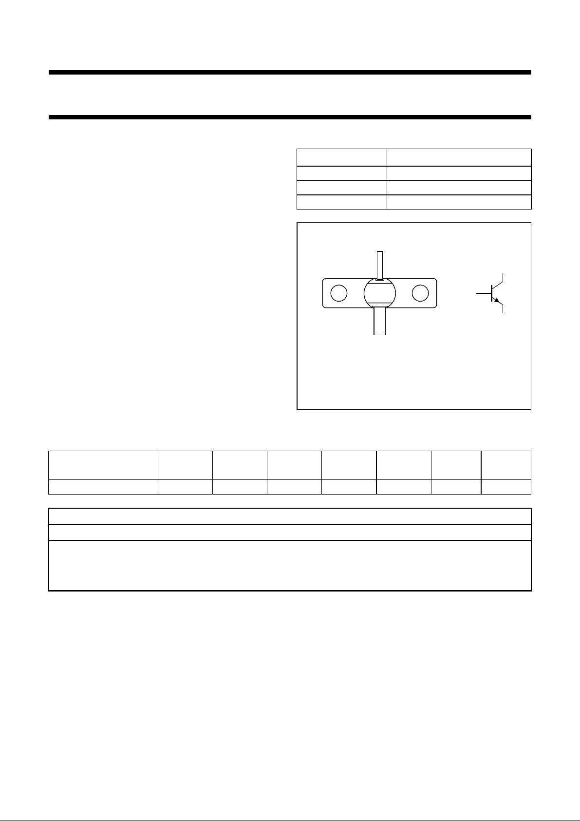
PINNING - SOT440A
PIN DESCRIPTION
1 collector
2 base
3 emitter connected to flange
olumns
Top view
Marking code: 502
Fig.1 Simplified outline and symbol.
1
c
b
3
2
MAM131
e
QUICK REFERENCE DATA
Microwave performance up to T
MODE OF OPERATION
=25°C in a common emitter class-A amplifier.
mb
f
(GHz)
V
(V)
CE
I
C
(mA)
P
L1
(mW)
G
po
(dB)
Z
(Ω)
i
Z
(Ω)
Class-A (CW) linear 4.2 18 110 ≥450 ≥6.6 100 + j40 4 + j4
WARNING
Product and environmental safety - toxic materials
This product contains beryllium oxide. The product is entirely safe provided that the BeO slab is not damaged.
All persons who handle, use or dispose of this product should be aware of its nature and of the necessary safety
precautions. After use, dispose of as chemical or special waste according to the regulations applying at the location of
the user. It must never be thrown out with the general or domestic waste.
L
1997 Feb 21 2
Philips Semiconductors Product specification
NPN microwave power transistor LTE42005S
LIMITING VALUES
In accordance with the Absolute Maximum Rating System (IEC 134).
SYMBOL PARAMETER CONDITIONS MIN. MAX. UNIT
V
CBO
V
CER
V
CEO
V
EBO
I
C
P
tot
T
stg
T
j
T
sld
collector-base voltage open emitter − 40 V
collector-emitter voltage RBE= 100 Ω−35 V
collector-emitter voltage open base − 16 V
emitter-base voltage open collector − 3V
collector current (DC) − 250 mA
total power dissipation Tmb≤ 75 °C − 4W
storage temperature −65 +200 °C
operating junction temperature − 200 °C
soldering temperature at 0.3 mm from case; t = 10 s − 235 °C
3
10
handbook, halfpage
I
C
(mA)
(3)
2
10
10
(1) (2)
CEO
V
15 20 25 30 35
VCE (V)
10
1
Tmb≤ 75°C.
(1) Region of permissible DC operation.
(2) Permissible extension provided RBE≤ 100 Ω.
(3) Second breakdown limit (independent of temperature).
Fig.2 DC SOAR.
MBH902
handbook, halfpage
5
P
tot
(W)
4
3
2
1
0
−50 200
0 50 100 150
MGD966
Tmb (°C)
Fig.3 Power dissipation derating as a function of
mounting-base temperature.
1997 Feb 21 3
 Loading...