


UM10120
Volume 1: LPC213x User Manual
Rev. 01 — 24 June 2005 User manual
Document information
Info Content
Keywords LPC2131, LPC2132, LPC2134, LPC2136, LPC2138, LPC2000, LPC213x,
ARM, ARM7, embedded, 32-bit, microcontroller
Abstract An initial LPC213x User Manual revision

Philips Semiconductors
Volume 1 LPC2131/2/4/6/8 UM
Revision history
Rev Date Description
01 20050624 Initial version
UM10120
Contact information
For additional information, please visit: http://www.semiconductors.philips.com
For sales office addresses, please send an email to: sales.addresses@www.semiconductors.philips.com
© Koninklijke Philips Electronics N.V. 2005. All rights reserved.
User manual Rev. 01 — 24 June 2005 2

1.1 Introduction
UM10120
Chapter 1: General information
Rev. 01 — 24 June 2005 User manual
The LPC2131/32/34/36/38 microcontrollers are based on a 16/32 bit ARM7TDMI-S™
CPU with real-time emulation and embedded trace support, that combines the
microcontroller with 32
Flash memory. A 128-bit wide memory interface and a unique accelerator architecture
enable 32-bit code execution at maximum clock rate. For critical code size applications,
the alternative 16-bit Thumb® Mode reduces code by more than 30
performance penalty.
Due to their tiny size and low power consumption, these microcontrollers are ideal for
applications where miniaturization is a key requirement, such as access control and
point-of-sale. With a wide range of serial comm unications interfaces and on-chip SRAM
options of 8/16/32
converters, soft modems, voice recognition and low end imaging, providing both large
buffer size and high processing power. Various 32-bit timers, single or dual 10-bit
8
channel ADC(s), 10-bit D AC, PWM channels and 47 GPIO lines with up to nine edge or
level sensitive external interrupt pins make these microcontrollers particularly suitable for
industrial control and medical systems.
kB, 64 kB, 128 kB, 256 kB and 512 kB of embedded high speed
% with minimal
kB, they are very well suited for communication gateways and protocol
1.2 Features
• 16/32-bit ARM7TDMI-S microcontroller in a tiny LQFP64 package
• 8/16/32 kB of on-chip static RAM and 32/64/128/256/512 kB of on-chip Flash program
memory. 128 bit wide interface/accelerator enables high speed 60
• In-System/In-Application Programming (ISP/IAP) via on-chip boot-loader software.
Single Flash sector or full chip erase in 400
• EmbeddedICE
on-chip RealMonitor™ software and high speed tracing of instruction execution.
®
and Embedded Trace interfaces offer real-time debugging with the
ms and 256 bytes programming in 1 ms.
• One (LPC2131/2) or two (LPC2134/6/8) 8 channel 10-bit A/D converters provide(s) a
total of up to 16 analog inputs, with conversion times as low as 2.44
• Single 10-bit D/A converter provides variable analog output. (LPC2132/4/6/8 only).
• Two 32-bit timers/external event counters (with four capture and four compare
channels each), PWM unit (six outputs) and watchdog.
• Low power Real-time clock with independent po wer an d dedicated 32 kHz clock input.
• Multiple serial interfaces including two UARTs (16C550), two Fast I
SPI™ and SSP with buffering and variable data length capabilities.
• Vectored interrupt controller with configurable priorities and vector addresses.
MHz operation.
µs per channel.
2
C (400 kbit/s),
© Koninklijke Philips Electronics N.V. 2005. All rights reserved.
User manual Rev. 01 — 24 June 2005 3

Philips Semiconductors
Volume 1 Chapter 1: Introductory information
• Up to 47 of 5 V tolerant general purpose I/O pins in tiny LQFP64 package.
• Up to nine edge or level sensitive external interrupt pins available.
• 60 MHz maximum CPU clock available from programmable on-chip Phase-Locked
Loop (PLL) with settling time of 100
• On-chip integrated oscillator operates with external crystal in range of 1 MHz to
30
• Power saving modes include Idle and Power-down.
• Individual enable/disable of peripheral functions as well as peripheral clock scaling
down for additional power optimization.
• Processor wake-up from Power-down mode via external interrupt or Real-time Clock.
• Single power supply chip with Power-On Reset (POR) and Brown-Out Detection
(BOD) circuits:
– CPU operating voltage range of 3.0 V to 3.6 V (3.3 V ± 10 %) with 5 V tolerant I/O
1.3 Applications
UM10120
µs.
MHz or with external oscillator from 1 MHz to 50 MHz.
pads
• Industrial control
• Medical systems
• Access control
• Point-of-sale
• Communication gateway
• Embedded soft modem
• General purpose applications
1.4 Device information
Table 1: LPC2131/2132/2134/2136/2138 device information
Device Number of
LPC2131 64 8 kB 32 kB 8 - LPC2132 64 16 kB 64 kB 8 1 LPC2134 64 16 kB 128 kB 16 1 UART1 with fu ll
LPC2136 64 32 kB 256 kB 16 1 UART1 with fu ll
LPC2138 64 32 kB 512 kB 16 1 UART1 with fu ll
pins
On-chip
SRAM
On-chip
FLASH
Number of
10-bit ADC
channels
Number of
10-bit DAC
channels
Note
modem interface
modem interface
modem interface
© Koninklijke Philips Electronics N.V. 2005. All rights reserved.
User manual Rev. 01 — 24 June 2005 4

Philips Semiconductors
Volume 1 Chapter 1: Introductory information
1.5 Architectural overview
The LPC2131/2/4/6/8 consists of an ARM7TDMI-S CPU with emulation support, the
ARM7 Local Bus for interface to on-chip memory controllers, the AMBA Advanced
High-performance Bus (AHB) for interface to the interrupt controller, and the VLSI
Peripheral Bus (VPB, a compatible superset of ARM’s AMBA Advanced Peripheral Bus)
for connection to on-chip peripheral functions. The LPC2131/2/4/6/8 configures the
ARM7TDMI-S processor in little-endian byte order.
AHB peripherals are allocated a 2 megabyte range of addresses at the very top of the
4
gigabyte ARM memory space. Each AHB peripheral is a llocated a 16 kB address space
within the AHB address space. LPC2131/2/4/6/8 peripheral functions (other than the
interrupt controller) are connected to the VPB bus. The AHB to VPB bridge interfaces the
VPB bus to the AHB bus. VPB peripherals are also allocated a 2
addresses, beginning at the 3.5
a 16
kB address space within the VPB address space.
The connection of on-chip peripherals to device pins is controlled by a Pin Connect Block
(see chapter "Pin Connect Block" on
specific application requirements for the use of peripheral functions and pins.
UM10120
megabyte range of
gigabyte address point. Each VPB peripheral is allocated
page 73). This must be configured by software to fit
1.6 ARM7TDMI-S processor
The ARM7TDMI-S is a general purpose 32-bit microprocessor, which offers high
performance and very low power consumption. The ARM architectu re is base d on
Reduced Instruction Set Computer (RISC) principles, and the instruction set and related
decode mechanism are much simpler than those of microprogrammed Complex
Instruction Set Computers. This simplicity results in a high instruction throughput and
impressive real-time interrupt response from a small and cost-effective processor core.
Pipeline techniques are employ ed so that all parts of the processing and memory systems
can operate continuously. Typically, while one instruction is being executed, its successor
is being decoded, and a third instruction is being fetched from memory.
The ARM7TDMI-S processor also employs a unique architectural strategy known as
THUMB, which makes it ideally suited to high-volume applications with memory
restrictions, or applications where code density is an issue.
The key idea behind THUMB is that of a super-reduced instruction set. Essentially, the
ARM7TDMI-S processor has two instruction sets:
• The standard 32-bit ARM instruction set.
• A 16-bit THUMB instruction set.
The THUMB set’s 16-bit instruction length allows it to approach twice the density of
standard ARM code while retaining most of the ARM’s performance advantage over a
traditional 16-bit processor using 16-bit registers. This is possible because THUMB code
operates on the same 32-bit register set as ARM code.
THUMB code is able to provide up to 65% of the code size of ARM, and 160% of the
performance of an equivalent ARM processor connecte d to a 16 -b it me m ory system.
© Koninklijke Philips Electronics N.V. 2005. All rights reserved.
User manual Rev. 01 — 24 June 2005 5

Philips Semiconductors
Volume 1 Chapter 1: Introductory information
The ARM7TDMI-S processor is described in detail in the ARM7TDMI-S Datasheet that
can be found on official ARM website.
1.7 On-chip Flash memory system
The LPC2131/2/4/6/8 incorporates a 32, 64, 128, 256 and 512 kB Flash memory system
respectively. This memory may be used for both code and data storage. Programming of
the Flash memory may be accomplished in several ways: over the serial builtin JTAG
interface, using In System Programming (ISP) and UART0, or by means of In Application
Programming (IAP) capabilities. The application program, using the IAP functions, may
also erase and/or program the Flash while the application is running, allowing a great
degree of flexibility for data storage field firmware upgrades, etc. When the
LPC2131/2/4/6/8 on-chip bootloader is used, 32/64/128/256/500 kB of Flash memory is
available for user code.
The LPC2131/2/4/6/8 Flash memory provides minimum of 10,000 er ase/write cycles and
10 years of data-retention.
1.8 On-chip Static RAM (SRAM)
UM10120
On-chip Static RAM (SRAM) may be used for code and/or data storage. The on-chip
SRAM may be accessed as 8-bits, 16-bits, and 32-bits. The LPC2131/2/4/6/8 provide
8/16/32 kB of static RAM respectively.
The LPC2131/2/4/6/8 SRAM is designed to be accessed as a byte-addressed memory.
Word and halfword accesses to the memory ignore the alignment of the address and
access the naturally-aligned value that is addressed (so a memory access ignores
address bits 0 and 1 for word accesses, and ignores bit 0 for halfword accesses).
Therefore valid reads and writes require data accessed as halfwords to originate from
addresses with address line 0 being 0 (addresses ending with 0, 2, 4, 6, 8, A, C, and E in
hexadecimal nottaion) and data accessed as words to originate from adresses with
address lines 0 and 1 being 0 (addresses ending with 0, 4, 8, and C in hexadecimal
notation). This rule applies to both off and on-chip memory usage.
The SRAM controller incorporates a write-back buffer in order to prevent CPU stalls during
back-to-bac k writes. The write-back buffer always holds the last data sent by software to
the SRAM. This data is only written to the SRAM when another write is requested by
software (the data is only written to the SRAM when sof tware does anot her write). If a chip
reset occurs, actual SRAM contents will not reflect the most recent write request (i.e. after
a "warm" chip reset, the SRAM does not reflect the last write oper ation). An y softwar e that
checks SRAM contents after reset must take this into account. Two identical writes to a
location guarantee that the data will be present after a Reset. Alternatively, a dummy write
operation before entering idle or power-down mode will similarly guarantee that the last
data written will be present in SRAM after a subsequent Reset.
© Koninklijke Philips Electronics N.V. 2005. All rights reserved.
User manual Rev. 01 — 24 June 2005 6
Philips Semiconductors
Volume 1 Chapter 1: Introductory information
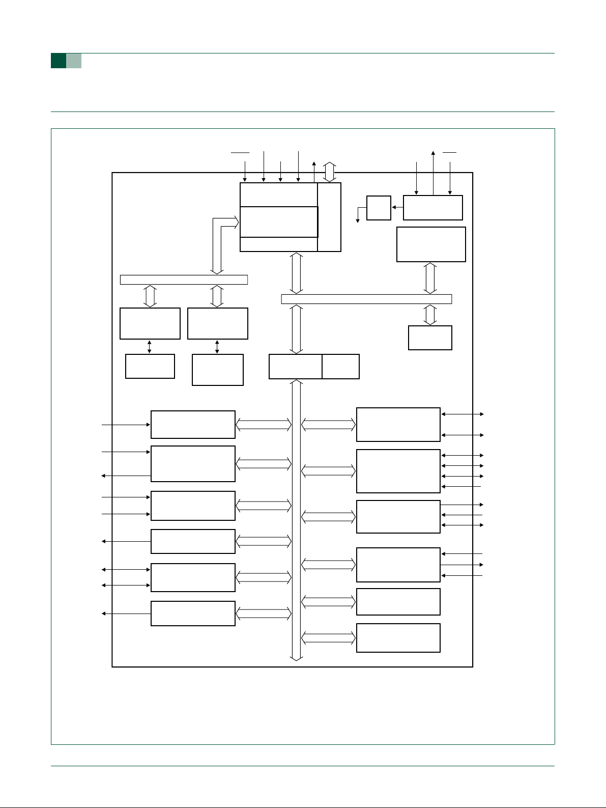
1.9 Block diagram
UM10120
EINT3:0
8 × CAP0
8 × MAT
AD0.7:0
AD1.7:0
AOUT
P0.31:0
P1.31:16
PWM6:1
LPC2131/2132/2134/2136/2138
ARM7 local bus
INTERNAL
SRAM
CONTROLLER
8/16/32 kB
SRAM
INTERRUPTS
TIMER 0/TIMER 1
A/D CONVERTERS
(1)
(2)
D/A CONVERTER
PURPOSE I/O
INTERNAL
CONTROLLER
32/64/128/
256/512 kB
EXTERNAL
CAPTURE/
COMPARE
(1)
0 AND 1
GENERAL
PWM0
FLASH
FLASH
(2)
TMS
(3)
TRST
ARM7TDMI-S
(3)
TDI
(3)
TCK
TEST/DEBUG
INTERFACE
AHB BRIDGE
AHB TO VPB
BRIDGE
(3)
(3)
TDO
PLL
MODULE
system
clock
EMULATION TRACE
(Advanced High-performance Bus)
VPB (VLSI
peripheral bus)
AMBA AHB
VPB
DIVIDER
2
I
C SERIAL
INTERFACES 0 AND 1
SPI AND SSP
SERIAL INTERFACES
UART0/UART1
REAL TIME CLOCK
WATCHDOG
TIMER
XTAL2
XTAL1
FUNCTIONS
VECTORED
INTERRUPT
CONTROLLER
RST
SYSTEM
AHB
DECODER
SCL0,1
SDA0,1
SCK0,1
MOSI0,1
MISO0,1
SSEL0,1
TXD0,1
RXD0,1
(1)
DSR1
(1)
RTS1
(1)
DCD1
RTXC1
RTXC2
V
BAT
,CTS1
, DTR1
(1)
,RI1
(1)
,
(1)
SYSTEM
CONTROL
002aab067
(1) LPC2134/2136/2138 only.
(2) LPC2132/2134/2136/2138 only.
(3) Pins shared with GPIO.
Fig 1. LPC2131/2/4/6/8 block diagram
© Koninklijke Philips Electronics N.V. 2005. All rights reserved.
User manual Rev. 01 — 24 June 2005 7

2.1 Memory maps
The LPC2131/2/4/6/8 incorporates several distinct memory regions, shown in the
following figures.
user program viewpoint following reset. The interrupt vector area supports address
remapping, which is described later in this section.
UM10120
Chapter 2: LPC2131/2/4/6/8 Memory Addressing
Rev. 01 — 24 June 2005 User manual
Figure 2 shows the overall map of the entire address space from the
4.0 GB
3.75 GB
3.5 GB
3.0 GB
2.0 GB
1.0 GB
AHB PERIPHERALS
VPB PERIPHERALS
RESERVED ADDRESS SPACE
BOOT BLOCK
(REMAPPED FROM ON-CHIP FLASH MEMORY)
32 kB ON-CHIP STATIC RAM (LPC2136/2138)
16 kB ON-CHIP STATIC RAM (LPC2132/2134)
8 kB ON-CHIP STATIC RAM (LPC2131)
RESERVED ADDRESS SPACE
0xFFFF FFFF
0xF000 0000
0xE000 0000
0xC000 0000
0x8000 0000
0x4000 8000
0x4000 7FFF
0x4000 4000
0x4000 3FFF
0x4000 2000
0x4000 1FFF
0x4000 0000
RESERVED ADDRESS SPACE
0x0008 0000
TOTAL OF 512 kB ON-CHIP NON-VOLATILE MEMORY
(LPC2138)
TOTAL OF 256 kB ON-CHIP NON-VOLATILE MEMORY
(LPC2136)
TOTAL OF 128 kB ON-CHIP NON-VOLATILE MEMORY
(LPC2134)
TOTAL OF 64 kB ON-CHIP NON-VOLATILE MEMORY
(LPC2132)
TOTAL OF 32 kB ON-CHIP NON-VOLATILE MEMORY
0.0 GB
Fig 2. System memory map
© Koninklijke Philips Electronics N.V. 2005. All rights reserved.
User manual Rev. 01 — 24 June 2005 8
(LPC2131)
0x0007 FFFF
0x0004 0000
0x0003 FFFF
0x0002 0000
0x0001 FFFF
0x0001 0000
0x0000 FFFF
0x0000 8000
0x0000 7FFF
0x0000 0000

Philips Semiconductors
Volume 1 Chapter 2: Memory map
UM10120
4.0 GB
4.0 GB - 2 MB
Notes:
- AHB section is
128 x 16 kB blocks
(totaling 2 MB).
- VPB section is
128 x 16 kB blocks
(totaling 2 MB).
3.75 GB
0xFFFF FFFF
AHB PERIPHERALS
0xFFE0 0000
0xFFDF FFFF
RESERVED
0xF000 0000
0xEFFF FFFF
RESERVED
3.5 GB + 2 MB
VPB PERIPHERALS
3.5 GB
Fig 3. Peripheral memory map
Figures 3 through 5 show differe nt views of the peripheral address space. Both the AHB
and VPB peripheral areas are 2 megabyte spaces which are divided up into 128
peripherals. Each peripheral space is 16 kilobytes in size. This allows simplifying the
© Koninklijke Philips Electronics N.V. 2005. All rights reserved.
User manual Rev. 01 — 24 June 2005 9
0xE020 0000
0xE01F FFFF
0xE000 0000
Philips Semiconductors
Volume 1 Chapter 2: Memory map
address decoding for each peripheral. All peripheral register addresses are word aligned
(to 32-bit boundaries) regardless of their size. This eliminates the need for byte lane
mapping hardware that would be required to allow byte (8-bit) or half-word (16-bit)
accesses to occur at smaller boundaries. An implication of this is that word and half-word
registers must be accessed all at once. For example, it is not possible to read or write the
upper byte of a word r egister separately.
UM10120
VECTORED INTERRUPT CONTROLLER
(AHB PERIPHERAL #126)
(AHB PERIPHERAL #125)
(AHB PERIPHERAL #124)
(AHB PERIPHERAL #3)
0xFFFF F000 (4G - 4K)
0xFFFF C000
0xFFFF 8000
0xFFFF 4000
0xFFFF 0000
0xFFE1 0000
0xFFE0 C000
(AHB PERIPHERAL #2)
0xFFE0 8000
(AHB PERIPHERAL #1)
0xFFE0 4000
(AHB PERIPHERAL #0)
0xFFE0 0000
Fig 4. AHB peripheral map
© Koninklijke Philips Electronics N.V. 2005. All rights reserved.
User manual Rev. 01 — 24 June 2005 10
Philips Semiconductors
Volume 1 Chapter 2: Memory map
UM10120
SYSTEM CONTROL BLOCK
(VPB PERIPHERAL #127)
(VPB PERIPHERALS #28-126)
NOT USED
DAC
(VPB PERIPHERAL #27)
SSP
(VPB PERIPHERAL #26)
NOT USED
(VPB PERIPHERAL #25)
10 BIT AD1 (LPC2138)
(VPB PERIPHERAL #24)
(VPB PERIPHERAL #23)
(VPB PERIPHERAL #14-22)
(VPB PERIPHERAL #13)
(VPB PERIPHERAL #12)
PIN CONNECT BLOCK
(VPB PERIPHERAL #11)
(VPB PERIPHERAL #10)
(VPB PERIPHERAL #9)
(VPB PERIPHERAL #8)
(VPB PERIPHERAL #7)
(VPB PERIPHERAL #6)
(VPB PERIPHERAL #5)
(VPB PERIPHERAL #4)
(VPB PERIPHERAL #3)
(VPB PERIPHERAL #2)
(VPB PERIPHERAL #1)
WATCHDOG TIMER
(VPB PERIPHERAL #0)
2
C1
I
NOT USED
10 BIT ADO
NOT USED
GPIO
RTC
SPI0
2
C0
I
NOT USED
PWM
UART1
URT0
TIMER1
TIMER0
0xE01F FFFF
0xE01F C000
0xE007 0000
0xE006 C000
0xE006 8000
0xE006 4000
0xE006 0000
0xE005 C000
0xE003 8000
0xE003 4000
0xE003 0000
0xE002 C000
0xE002 8000
0xE002 4000
0xE002 0000
0xE001 C000
0xE001 8000
0xE001 4000
0xE001 0000
0xE000 C000
0xE000 8000
0xE000 4000
0xE000 0000
Fig 5. VPB peripheral map
© Koninklijke Philips Electronics N.V. 2005. All rights reserved.
User manual Rev. 01 — 24 June 2005 11

Philips Semiconductors
Volume 1 Chapter 2: Memory map
UM10120
2.2 LPC2131/2132/2134/2136/2138 memory re-mapping and boot block
2.2.1 Memory map concepts and operating modes
The basic concept on the LPC2131/2/4/6/8 is that each memory area has a "natural"
location in the memory map. This is the address ran ge f or which code re siding in that area
is written. The bulk of each memory space remains permanently fixed in the same
location, eliminating the need to have portions of the code designed to run in different
address ranges.
Because of the location of the interrupt vectors on the ARM7 processor (at addresses
0x0000
Boot Block and SRAM spaces need to be re-mapped in order to allow alternative uses of
interrupts in the different operating modes described in
interrupts is accomplished via the Memory Mapping Control feature ( Section 3. 6 “Memory
mapping control” on page 25).
Table 2: ARM exception vector locations
Address Exception
0x0000 0000 Reset
0x0000 0004 Undefined Instruction
0x0000 0008 Software Interrupt
0x0000 000C Prefetch Abort (instruction fetch memory fault)
0x0000 0010 Data Abort (data access memory fault)
0x0000 0014 Reserved
0x0000 0018 IRQ
0x0000 001C FIQ
0000 through 0x0000 001C, as shown in Table 2 below), a small portion of the
Table 3. Re-mapping of the
Note: Identified as reserved in ARM documentation, this location is used
by the Boot Loader as the Valid User Program key. This is descibed in
detail in "Flash Memory System and Programming" chapter on
page 216.
Table 3: LPC2131/2/4/6/8 memory mapping modes
Mode Activation Usage
Boot
Loader
mode
User
Flash
mode
User RAM
mode
© Koninklijke Philips Electronics N.V. 2005. All rights reserved.
User manual Rev. 01 — 24 June 2005 12
Hardware
activation by
any Reset
Software
activation by
Boot code
Software
activation by
User program
The Boot Loader always executes after any reset. The Boot Block
interrupt vectors are mapped to the bottom of memory to allow
handling exceptions and using interrupts during the Boot Loading
process.
Activated by Boot Loader when a valid User Program Signature is
recognized in memory and Boot Loader operation is not forced.
Interrupt vectors are not re-mapped and are found in the bottom of the
Flash memory.
Activated by a User Program as desired. Interrupt vectors are
re-mapped to the bottom of the Static RAM.

Philips Semiconductors
Volume 1 Chapter 2: Memory map
2.2.2 Memory re-mapping
In order to allow for compatibility with future derivatives, the entire Boot Block is mapped
to the top of the on-chip memory space. In this manner, the use of larger or smaller flash
modules will not require changing the location of the Boot Block (which would require
changing the Boot Loader code itself) or changin g the mapping of t he Boot Bloc k interrupt
vectors. Memory spaces other than the interrupt vectors remain in fixed locations.
Figure 6 shows the on-chip memory mapping in the modes defined above.
The portion of memory that is re-mapped to allow interrupt processing in different modes
includes the interrupt vector area (32
64
bytes. The re-mapped code locations overlay addresses 0x0000 0000 through
0x0000
handler at address 0x0000
vector contained in the SRAM, e xternal memory, and Boot Block must contain br anches to
the actual interrupt handlers, or to other instructions that accomplish the branch to the
interrupt handlers.
There are three reasons this configuration was chosen:
1. To give the FIQ handler in t he Flash memory the advantage of not having to take a
memory boundary caused by the remapping into account.
2. Minimize the need to for the SRAM and Boot Block vectors to deal with arbitrary
boundaries in the middle of code space.
3. To provide space to store constants for jumping beyond the range of single word
branch instructions.
UM10120
bytes) and an additional 32 bytes, for a total of
003F. A typical user program in the Flash memory can place the entire FIQ
001C without any need to consider memory boundaries. The
Re-mapped memory areas, including the Boot Block and interrupt vectors, continue to
appear in their original location in addition to the re-mapped address.
Details on re-mapping and examples can be found in Section 3.6 “ Memory mapping
control” on page 25.
© Koninklijke Philips Electronics N.V. 2005. All rights reserved.
User manual Rev. 01 — 24 June 2005 13
Philips Semiconductors
Volume 1 Chapter 2: Memory map
2.0 GB - 12 kB
2.0 GB
12 kB BOOT BLOCK
(RE-MAPPED FROM TOP OF FLASH MEMORY)
(BOOT BLOCK INTERRUPT VECTORS)
RESERVED ADDRESSING SPACE
UM10120
0x8000 0000
0x7FFF FFFF
1.0 GB
32 kB ON-CHIP SRAM
(SRAM INTERRUPT VECTORS)
RESERVED ADDRESSING SPACE
(12 kB BOOT BLOCK RE-MAPPED TO HIGHER ADDRESS RANGE)
512 kB FLASH MEMORY
0x4000 8000
0x4000 7FFF
0x4000 0000
0x3FFF FFFF
0x0008 0000
0x0007 FFFF
0.0 GB
Note: Memory regions are not drawn to scale.
Fig 6. Map of lower memory is showing re-mapped and re-mappable areas (LPC2138
with 512 kB Flash)
© Koninklijke Philips Electronics N.V. 2005. All rights reserved.
User manual Rev. 01 — 24 June 2005 14
ACTIVE INTERRUPT VECTORS (FROM FLASH, SRAM, OR BOOT BLOCK)
0x0000 0000

Philips Semiconductors
Volume 1 Chapter 2: Memory map
2.3 Prefetch abort and data abort exceptions
The LPC2131/2/4/6/8 generates the approp riate bus cycle abort exception if an access is
attempted for an a ddress t hat is in a re serve d or u nassign ed addre ss r eg ion. T he regi ons
are:
• Areas of the memory map that are not implemented for a specific ARM derivative. F or
the LPC2131/2/4/6/8, this is:
– Address space between On-Chip Non-Volatile Memory and On-Chip SRAM,
labelled "Reserved Address Space" in
device this is memory address range from 0x0000 8000 to 0x3FFF FFFF, for 64 kB
Flash device this is memory address range from 0x0001
128
kB Flash device this is memory address range from 0x0002 0000 to
0x3FFF
0x0004
0x0008
– Address space between On-Chip Static RAM and the Boot Block. Labelled
"Reserved Address Space" in
address range from 0x4000 2000 to 0x7FFF CFFF, for 16 kB SRAM device this is
memory address range from 0x4000
device this range is from 0x4000
– Address space between 0x8000 0000 and 0xDFFF FFFF, labelled "Reserved
Adress Space".
– Reserved regions of the AHB and VPB spaces. See Figure 3.
• Unassigned AHB peripheral spaces. See Figure 4.
• Unassigned VPB peripheral spaces. See Figure 5.
FFFF, for 256 kB Flash device this is memory address range from
0000 to 0x3FFF FFFF while for 512 kB Flash device this range is from
0000 to 0x3FFF FFFF.
Figure 2. For 8 kB SRAM device this is memory
8000 to 0x7FFF CFFF.
UM10120
Figure 2 and Figure 6. For 32 kB Flash
0000 to 0x3FFF FFFF, for
4000 to 0x7FFF CFFF, while for 32 kB SRAM
For these areas , both at tempt ed data access and inst ruction fetch generate an exception.
In addition, a Prefetch Abort exception is generated for any instruction fetch that maps to
an AHB or VPB peripheral address.
Within the address space of an existing VPB peripheral , a data abort exception is not
generated in response to an access to an undefined address. Address decoding within
each peripheral is limited to that needed to distinguish defined registers within the
peripheral itself. For example, an access to address 0 xE000
within the UART0 space) may result in an access to the register defined at address
0xE000
in the LPC2131/2/4/6/8 documentation and are not a supported feature.
Note that the ARM core stores the Prefetch Abort flag along with the associated
instruction (which will be meaningless) in the pipeline and processes the abort only if an
attempt is made to execute the instruction fetched from the illegal address. This prevents
accidental aborts that could be caused by prefetches that occur when code is executed
very near a memory boundary.
C000. Details of such address aliasing within a peripheral space are not defined
D000 (an undefined address
© Koninklijke Philips Electronics N.V. 2005. All rights reserved.
User manual Rev. 01 — 24 June 2005 15

UM10120
Chapter 3: System Control Block
Rev. 01 — 24 June 2005 User manual
3.1 Summary of system control block functions
The System Control Block includes several system features and control registers for a
number of functions that are not related to specific peripheral devices. These include:
• Crystal Oscillator
• External Interrupt Inputs
• Memory Mapping Control
• PLL
• Power Contro l
• Reset
• VPB Divider
• Wakeup Timer
Each type of function has its own register(s) if any are required and unneeded bits are
defined as reserved in order to allow future expansion. Unrelated functions never share
the same register addresses
3.2 Pin description
Table 4 shows pins that are associated with System Control block functions.
Table 4: Pin summary
Pin name Pin
X1 Input Crystal Oscillator Input - Input to the oscillator and internal clock
X2 Output Crystal Oscillator Output - Output from the oscillator amplifier
EINT0 Input External Interrupt Input 0 - An active low/high level or
EINT1 Input External Interrupt Input 1 - See the EINT0 description above.
Pin description
direction
generator circuits
falling/rising edge general purpose interrupt input. This pin may be
used to wake up the processor from Idle or Power-down modes.
Pins P0.1 and P0.16 can be selected to perform EINT0 function.
Pins P0.3 and P0.14 can be selected to perform EINT1 function.
Important: LOW level on pin P0.14 immediately after reset is
considered as an external hardware request to start the ISP
command handler. More details on ISP and Serial Boot Loader can
be found in "Flash Memory System and Programming" chapter on
page 216.
© Koninklijke Philips Electronics N.V. 2005. All rights reserved.
User manual Rev. 01 — 24 June 2005 16

Philips Semiconductors
Volume 1 Chapter 3: System Control Block
Table 4: Pin summary
Pin name Pin
EINT2 Input External Interrupt Input 2 - See the EINT0 description above.
EINT3 Input External Interrupt Input 3 - See the EINT0 description above.
RESET Input External Reset input - A LOW on this pin resets the chip, causing
3.3 Register description
All registers, regardless of size, are on word address boundaries. Details of the registers
appear in the description of each function.
Table 5: Summary of system control registers
Name Description Access Reset
External Interrupts
EXTINT External Interrupt Flag Register R/W 0 0xE01F C140
EXTWAKE External Interrupt Wakeup Register R/W 0 0xE01F C144
EXTMODE External Interrupt Flag register R/W 0 0xE01F C148
EXTPOLAR External Interrupt Wakeup Register R/W 0 0xE01F C14C
Memory Mapping Control
MEMMAP Memory Mapping Control R/W 0 0xE01F C040
Phase Locked Loop
PLLCON PLL Control Register R/W 0 0xE01F C080
PLLCFG PLL Configuration Register R/W 0 0xE01F C084
PLLSTAT PLL Status Register RO 0 0xE01F C088
PLLFEED PLL Feed Register WO NA 0xE01F C08C
Power Control
PCON Power Control Register R/W 0 0xE01F C0C0
PCONP Power Control for Peripherals R/W 0x03BE 0xE01F C0C4
VPB Divider
VPBDIV VPB Divider Control R/W 0 0xE01F C100
Reset
RSID Reset Source Identification Register R/W 0 0xE01F C180
Code Security/Debugging
CSPR Code Secur ity Protection Register RO o 0xE01F C184
direction
UM10120
Pin description
Pins P0.7 and P0.15 can be selected to perform EINT2 function.
Pins P0.9, P0.20 and P0.30 can be selected to perform EINT3
function.
I/O ports and peripherals to take on their default states, and the
processor to begin execution at address 0x0000
value
0000.
Address
[1]
[1] Reset value relects the data stored in used bits only. It does not include reserved bits content.
© Koninklijke Philips Electronics N.V. 2005. All rights reserved.
User manual Rev. 01 — 24 June 2005 17
Philips Semiconductors
Volume 1 Chapter 3: System Control Block
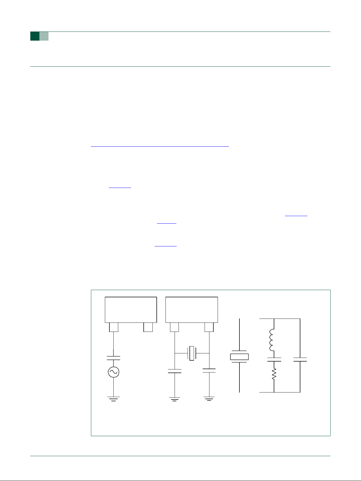
3.4 Crystal oscillator
While an input signal of 50-50 duty cycle within a frequency range from 1 MHz to 50 MHz
can be used by the LPC2131/2/4/6/8 if supplied to its input XTAL1 pin, this
microcontroller’s onboard oscillator circuit supports external crystals in the range of 1
to 30
MHz only. If the on-chip PLL system or the boot-loader is used, the inp ut clock
frequency is limited to an exclusive range of 10
UM10120
MHz
MHz to 25 MHz.
The oscillator output frequency is called F
referred to as CCLK f or purposes of rate equations , etc. else where in this d ocument. F
and the ARM processor clock frequency is
OSC
OSC
and CCLK are the same value unless the PLL is running and connected. Refer to the
Section 3.7 “Phase Locked Loop (PLL)” on page 26 for details and frequency limitations.
The onboard oscillator in the LPC2131/2/4/6/8 can operate in one of two modes: slave
mode and oscillation mode.
In slave mode th e input clock signal should be coupled by means of a capacitor of 100 pF
(C
in Figure 7, drawing a), with an amplitude of at least 200 mVrms. The X2 pin in this
C
configuration can be left not connected. If sla ve mode is se lected, the F
duty cycle can range from 1
MHz to 50 MHz.
signal of 50-50
OSC
External components and models used in oscillation mode are shown in Figure 7,
drawings b and c, and in Table 6. Since the feedbac k resistance is int egr ated on chip, only
a crystal and the capacitances CX1 and CX2 need to be connected externally in case of
fundamental mode oscillation (the fundamental frequency is represented by L, C
R
). Capacitance CP in Figure 7, drawing c, represents the parallel package capacitance
S
and
L
and should not be larger than 7 pF. Param eters FC, CL, RS and CP are supplied by the
crystal manufacturer.
Choosing an oscillation mode as an on-board oscillator mode of operation limits F
clock selection to 1
MHz to 30 MHz.
OSC
LPC2131/2/4/6/8 LPC2131/2/4/6/8
X1X1 X2X2
L
C
C
Clock
a) b) c)
Fig 7. Oscillator modes and m ode ls: a) slave mode of operation, b) oscillation mode of
operation, c) external crystal model used for C
© Koninklijke Philips Electronics N.V. 2005. All rights reserved.
User manual Rev. 01 — 24 June 2005 18
C
X1
Xtal
C
X2
X1/X2
< = >
evaluation
C
L
R
S
C
P
Philips Semiconductors
Volume 1 Chapter 3: System Control Block
UM10120
Table 6: Recommended values for C
in oscillation mode (crystal and external
X1/X2
components parameters)
Fundamental
oscillation frequency
F
C
Crystal load
capacitance C
Maximum crystal
L
series resistance R
External load
capacitors CX1,
S
1 MHz - 5 MHz 10 pF NA NA
20 pF NA NA
30 pF < 300 Ω 58 pF, 58 pF
5 MHz - 10 MHz 10 pF < 300 Ω 18 pF, 18 pF
20 pF < 300 Ω 38 pF, 38 pF
30 pF < 300 Ω 58 pF, 58 pF
10 MHz - 15 MHz 10 pF < 300 Ω 18 pF, 18 pF
20 pF < 220 Ω 38 pF, 38 pF
30 pF < 140 Ω 58 pF, 58 pF
15 MHz - 20 MHz 10 pF < 220 Ω 18 pF, 18 pF
20 pF < 140 Ω 38 pF, 38 pF
30 pF < 80 Ω 58 pF, 58 pF
20 MHz - 25 MHz 10 pF < 160 Ω 18 pF, 18 pF
20 pF < 90 Ω 38 pF, 38 pF
30 pF < 50 Ω 58 pF, 58 pF
25 MHz - 30 MHz 10 pF < 130 Ω 18 pF, 18 pF
20 pF < 50 Ω 38 pF, 38 pF
30 pF NA NA
CX2
f
selection
OSC
True
True
MIN f
= 10 MHz
OSC
MAX f
(Figure 7, mode a and/or b) (Figure 7, mode a) (Figure 7, mode b)
Fig 8. F
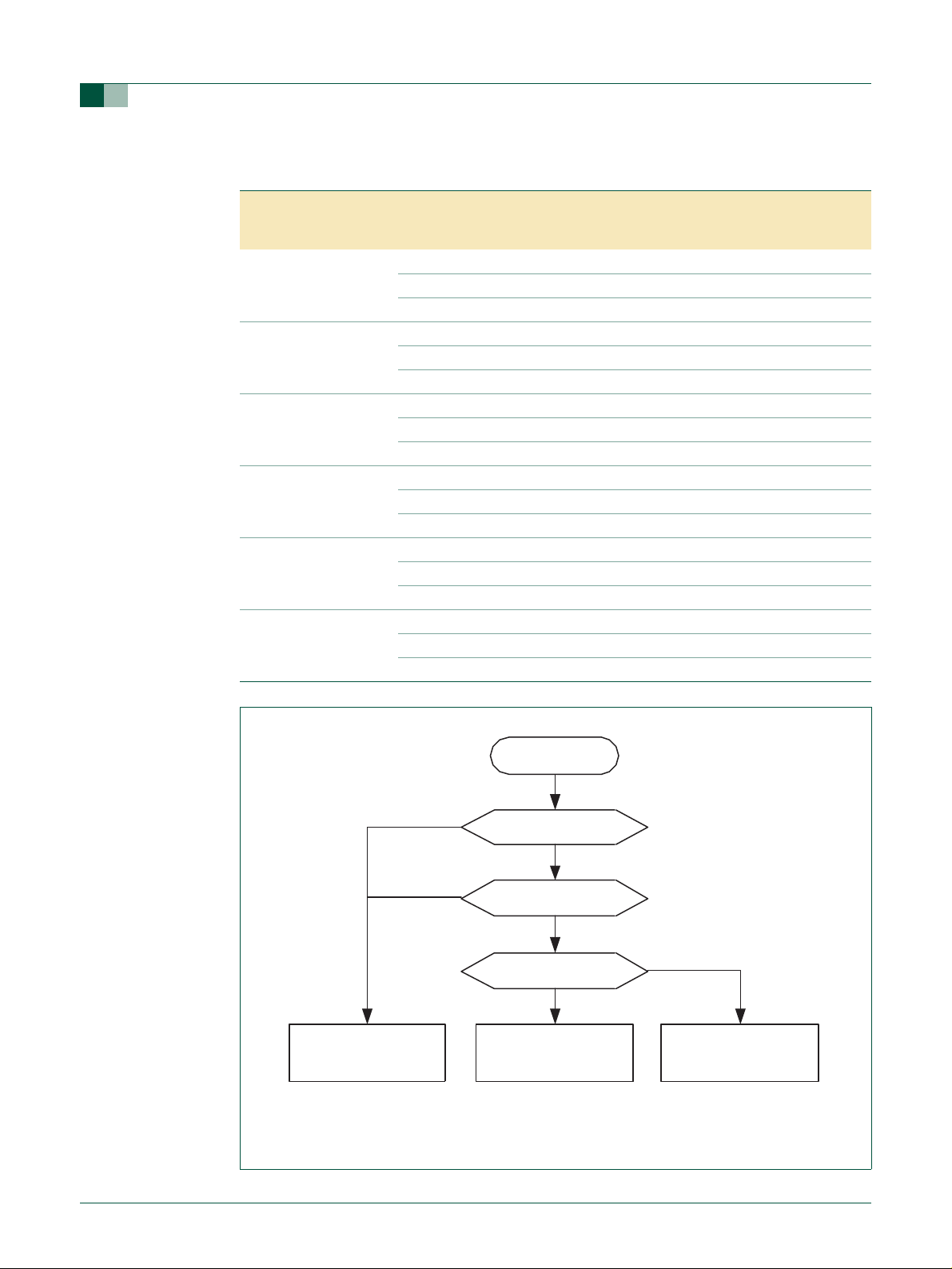
© Koninklijke Philips Electronics N.V. 2005. All rights reserved.
User manual Rev. 01 — 24 June 2005 19
OSC
= 25 MHz
OSC
selection algorithm
On-chip PLL used
in application?
False
ISP used for initial
code download?
False
External crystal
oscillator used?
False
MIN f
= 1 MHz
OSC
MAX f
= 50 MHz
OSC
True
MIN f
MAX f
= 1 MHz
OSC
= 30 MHz
OSC

Philips Semiconductors
Volume 1 Chapter 3: System Control Block
3.5 External interrupt inputs
The LPC2131/2/4/6/8 includes four External Interrupt Inputs as selectable pin functions.
The External Interrupt Inputs can optionally be used to wake up the processor from
Power-down mode.
3.5.1 Register description
The external interrupt function has four registers associated with it. The EXTINT register
contains the interrupt flags, and the EXTWAKEUP register contains bits that enable
individual external interrupts to wake up the microcontroller from Power-down mode. The
EXTMODE and EXTPOLAR registers specify the level and edge sensitivity parameters.
Table 7: External interrupt registers
Name Description Access Reset
EXTINT The External In terrupt Flag Register contains
interrupt flags for EINT0, EINT1, EINT2 and
EINT3. See
INTWAKE The Interrupt Wakeup Register contains four
enable bits that control whether each external
interrupt will cause the processor to wake up
from Power-down mode. See
EXTMODE The External Interrupt Mode Register controls
whether each pin is edge- or levelsensitive.
EXTPOLAR The External Interrupt Polarity Register controls
which level or edge on each pin will cause an
interrupt.
Table 8.
Table 9.
UM10120
Address
[1]
value
R/W 0 0xE01F C140
R/W 0 0xE01F C144
R/W 0 0xE01F C148
R/W 0 0xE01F C14C
[1] Reset value relects the data stored in used bits only. It does not include reserved bits content.
3.5.2 External Interrupt Flag register (EXTINT - 0xE01F C140)
When a pin is selected for its external interrupt function, the level or edge on that pin
(selected by its bits in the EXTPOLAR and EXTMODE registers) will set its interrupt flag in
this register. This asserts the corresponding interrupt request to the VIC, which will cause
an interrupt if interrupts from the pin are enabled.
Writing ones to bits EINT0 through EINT3 in EXTINT register clears the corresponding
bits. In level-sensitive mode this action is efficacious only when the pin is in its inactive
state.
Once a bit from EINT0 to EINT3 is set and an appropriate code starts to e xecut e (handling
wakeup and/or external interrupt), this bit in EXTINT register must be cleared. Otherwise
the event that was just triggered by activity on the EINT pin will not be recognized in the
future.
Important: whenever a change of external interrupt operating mode (i.e. active
level/edge) is performed (including the initialization of an external interrupt), the
corresponding bit in the EXTINT register must be cleared! For details see
3.5.4 “External Interrupt Mode register (EXTMODE - 0xE01F C148)” and Section 3.5.5
“External Interrupt Polarity register (EXTPOLAR - 0xE01F C14C)”.
Section
© Koninklijke Philips Electronics N.V. 2005. All rights reserved.
User manual Rev. 01 — 24 June 2005 20

Philips Semiconductors
Volume 1 Chapter 3: System Control Block
For example, if a system wakes up from power-down using a low level on external
interrupt 0 pin, its post-wakeup code m ust reset the EINT0 bit in order to allow futur e entry
into the power-down mode. If the EINT0 bit is left set to 1, subsequent attempt(s) to invoke
power-down mode will fail. The same goes for external interrupt handling.
More details on power-down mode will be discussed in the following chapters.
Table 8: External Interrupt Flag register (EXTINT - address 0xE01F C140) bit description
Bit Symbol Description Reset
0 EINT0 In le v el-sensitiv e mode, this bit is set if the EINT0 function is selected for its pin, and the pin is in
its active state. In edge-sensitive mode, this bit is set if the EINT0 function is selected for its pin,
and the selected edge occurs on the pin.
Up to two pins can be selected to perform the EINT0 function (see P0.1 and P0.16 description in
"Pin Configuration" chapter
This bit is cleared by writing a one to it, except in level sensitive mode when the pin is in its activ e
state (e.g. if EINT0 is selected to be low level sensitive and a low level is present on the
corresponding pin, this bit can not be cleared; this bit can be cleared only when the signal on the
pin becomes high).
1 EINT1 In le v el-sensitiv e mode, this bit is set if the EINT1 function is selected for its pin, and the pin is in
its active state. In edge-sensitive mode, this bit is set if the EINT1 function is selected for its pin,
and the selected edge occurs on the pin.
Up to two pins can be selected to perform the EINT1 function (see P0.3 and P0.14 description in
"Pin Configuration" chapter on page 64.)
This bit is cleared by writing a one to it, except in level sensitive mode when the pin is in its active
state (e.g. if EINT1 is selected to be low level sensitive and a low level is present on the
corresponding pin, this bit can not be cleared; this bit can be cleared only when the signal on the
pin becomes high).
2 EINT2 In le v el-sensitiv e mode, this bit is set if the EINT2 function is selected for its pin, and the pin is in
its active state. In edge-sensitive mode, this bit is set if the EINT2 function is selected for its pin,
and the selected edge occurs on the pin.
Up to two pins can be selected to perform the EINT2 function (see P0.7 and P0.15 description in
"Pin Configuration" chapter on page 64.)
This bit is cleared by writing a one to it, except in level sensitive mode when the pin is in its active
state (e.g. if EINT2 is selected to be low level sensitive and a low level is present on the
corresponding pin, this bit can not be cleared; this bit can be cleared only when the signal on the
pin becomes high).
3 EINT3 In le v el-sensitiv e mode, this bit is set if the EINT3 function is selected for its pin, and the pin is in
its active state. In edge-sensitive mode, this bit is set if the EINT3 function is selected for its pin,
and the selected edge occurs on the pin.
Up to three pins can be selected to perform the EINT3 function (see P0.9, P0.20 and P0.30
description in "Pin Configuration" chapter on page 64.)
This bit is cleared by writing a one to it, except in level sensitive mode when the pin is in its active
state (e.g. if EINT3 is selected to be low level sensitive and a low level is present on the
corresponding pin, this bit can not be cleared; this bit can be cleared only when the signal on the
pin becomes high).
7:4 - Reserved, user software should not write ones to reserved bits. The value read from a reserved
bit is not defined.
page 64.)
UM10120
value
0
0
0
0
NA
© Koninklijke Philips Electronics N.V. 2005. All rights reserved.
User manual Rev. 01 — 24 June 2005 21

Philips Semiconductors
Volume 1 Chapter 3: System Control Block
3.5.3 Interrupt Wakeup register (INTWAKE - 0xE01F C144)
Enable bits in the INTWAKE register allow the external interrupts to wake up the
processor if it is in Po we r-do wn mode . The relate d EINTn function m ust be mapped to the
pin in order for the wakeup process to take place. It is not necessary for the interrupt to be
enabled in the Vectored Interrupt Controller for a wakeup to take place. This arrang ement
allows additional capabilities, such as having an external interrupt input wake up the
processor from P ower-down mode without causing an interrupt (simply resuming
operation), or allowing an interrupt to be enabled during Power-down without waking the
processor up if it is asserted (eliminating the need to disable the interrupt if the wakeup
feature is not desirable in the application).
For an external interrupt pin to be a source that would wake up the microcontroller from
Po wer-down mode, it is also necessary to clear the corresponding bit in the External
Interrupt Flag register (
Table 9: Interrupt Wakeup register (INTW AKE - address 0xE01F C144) bit description
Bit Symbol Description Reset
0 EXTWAKE0 When one, assertion of EINT0 will wake up the processor from
1 EXTWAKE1 When one, assertion of EINT1 will wake up the processor from
2 EXTWAKE2 When one, assertion of EINT2 will wake up the processor from
3 EXTWAKE3 When one, assertion of EINT3 will wake up the processor from
13:4 - Reserved, user software should not write ones to reserved bits.
14 BODWAKE When one, a BOD interrupt will wake up the processor from
15 RTCWAKE When one, assertion of an RTC interrupt will wake up the
Section 3.5.2 on page 20).
Power-down mode.
Power-down mode.
Power-down mode.
Power-down mode.
The value read from a reserved bit is not defined.
Power-down mode.
processor from Power-down mode.
UM10120
value
0
0
0
0
NA
0
0
3.5.4 External Interrupt Mode register (EXTMODE - 0xE01F C148)
The bits in this register select whether each EINT pin is level- or edge-sensitive. Only pins
that are selected for the EINT function (see chapter Pin Connect Block on
enabled via the VICIntEnable register (Section 5.4.4 “Interrupt Enable register
(VICIntEnable - 0xFFFF F010)” on page 52) can cause interrupts from the External
Interrupt function (though of course pins selected for other functions may cause interrupts
from those functions).
Note: Software should only change a bit in this register when its interrupt is
disabled in the VICIntEnable register, and should write the corresponding 1 to the
EXTINT register before enabling (initializing) or re-enabling the interrupt, to clear
the EXTINT bit that could be set by changing the mode.
© Koninklijke Philips Electronics N.V. 2005. All rights reserved.
User manual Rev. 01 — 24 June 2005 22
page 73) and

Philips Semiconductors
Volume 1 Chapter 3: System Control Block
Table 10: External Interrupt Mode register (EXTMODE - address 0xE01F C148) bit
Bit Symbol Value Description Reset
0 EXTMODE0 0 Level-sensitivity is selected for EINT0. 0
1 EXTMODE1 0 Level-sensitivity is selected for EINT1. 0
2 EXTMODE2 0 Level-sensitivity is selected for EINT2. 0
3 EXTMODE3 0 Level-sensitivity is selected for EINT3. 0
7:4 - - Reserved, user software should not write ones to reserved
3.5.5 External Interrupt Polarity register (EXTPOLAR - 0xE01F C14C)
In level-sensitive mode, the bits in this register select whether the corresponding pin is
high- or low-active. In edge-sensitive mode, they select whether the pin is rising- or
falling-edge sensitive . Only pins that are selected for the EINT function (see "Pin Connect
Block" chapter on
“Interrupt Enable register (VICIntEnable - 0xFFFF F010)” on page 52) can cause
interrupts from the External Interrupt function (though of course pins selected for other
functions may cause interrupts from those functio ns ).
UM10120
description
value
1 EINT0 is edge sensitive.
1 EINT1 is edge sensitive.
1 EINT2 is edge sensitive.
1 EINT3 is edge sensitive.
NA
bits. The value read from a reserved bit is not defined.
page 73) and enabled in the VICIntEnable register (Section 5.4.4
Note: Software should only change a bit in this register when its interrupt is
disabled in the VICIntEnable register, and should write the corresponding 1 to the
EXTINT register before enabling (initializing) or re-enabling the interrupt, to clear
the EXTINT bit that could be set by changing the polarity.
Table 11: External Interrupt Polarity register (EXTPOLAR - address 0xE01F C14C) bit
description
Bit Symbol Value Description Reset
value
0 EXTPOLAR0 0 EINT0 is low-active or falling-edge sensitive (depending on
EXTMODE0).
1 EINT0 is high-active or rising-edge sensitive (depending on
EXTMODE0).
1 EXTPOLAR1 0 EINT1 is low-active or falling-edge sensitive (depending on
EXTMODE1).
1 EINT1 is high-active or rising-edge sensitive (depending on
EXTMODE1).
2 EXTPOLAR2 0 EINT2 is low-active or falling-edge sensitive (depending on
EXTMODE2).
1 EINT2 is high-active or rising-edge sensitive (depending on
EXTMODE2).
0
0
0
© Koninklijke Philips Electronics N.V. 2005. All rights reserved.
User manual Rev. 01 — 24 June 2005 23

Philips Semiconductors
Volume 1 Chapter 3: System Control Block
Table 11: External Interrupt Polarity register (EXTPOLAR - address 0xE01F C14C) bit
Bit Symbol Value Description Reset
3 EXTPOLAR3 0 EINT3 is low-active or falling-edge sensitive (depending on
7:4 - - Reserved, user software should not write ones to reserved
3.5.6 Multiple external interrupt pins
Software can select multiple pins f or each of EINT3:0 in t he Pin Select registers , which are
described in chapter Pin Connect Block on
of EINT3:0 receives the state of all of its associated pins from the pins’ receivers, along
with signals that indicate whether each pin is selected for the EINT function. The external
interrupt logic handles the case when more than one pin is so selected, diff erently
according to the state of its Mode and Polarity bits:
UM10120
description
value
0
EXTMODE3).
1 EINT3 is high-active or rising-edge sensitive (depending on
EXTMODE3).
NA
bits. The value read from a reserved bit is not defined.
page 73. The external interrupt logic for each
• In Low-Active Le v el Sensitiv e mode , the states o f all pins selected f or the same EINTx
functionality are digitally combined using a positive logic AND gate.
• In High-Active Level Sensitive mode, the states of all pins selected for the same
EINTx functionality are digitally combined using a positive logic OR gate.
• In Edge Sensitive mode, regardless of polarity, the pin with the lowest GPIO port
number is used. (Selecting multiple pins for an EINTx in edge-sensitive mode could
be considered a programming error.)
The signal derived by this logic is the EINTi signal in the following logic schematic
Figure 9.
For ex ample, if the EINT3 function is selected in the PINSEL0 and PINSEL1 registers for
pins P0.9, P0.20 and P0.30, and EINT3 is configured to be low level sensitive, the inputs
from all three pins will be logically ANDed. When more than one EINT pin is logically
ORed, the interrupt service routine can read the states of the pins from the GPIO port
using the IO0PIN and IO1PIN registers, to determine which pin(s) caused the interrupt.
© Koninklijke Philips Electronics N.V. 2005. All rights reserved.
User manual Rev. 01 — 24 June 2005 24
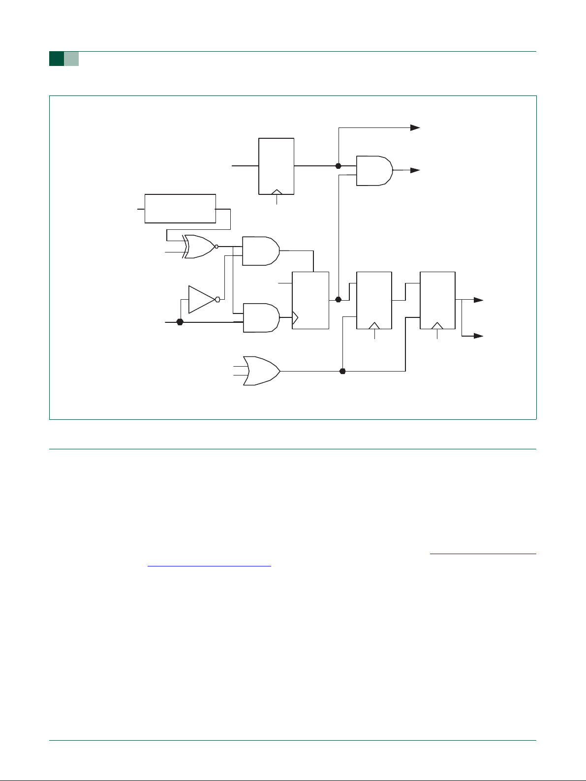
Philips Semiconductors
r
Volume 1 Chapter 3: System Control Block
UM10120
VPB Bus Data
EINTi
EXTPOLARi
EXTMODEi
Fig 9. External interrupt logic
GLITCH
FILTER
Write 1 to EXTINTi
Wakeup enable
(one bit of EXTWAKE)
D Q
PCLK
Reset
VPB Read
of EXTWAKE
EINTi to
Wakeup Time
(Figure 11)
Interrupt Flag
(one bit of EXTINT)
S
D
1
Q
R
S
R
PCLK
S
Q
Q
R
PCLK
3.6 Memory mapping control
The Memory Mapping Control alters the mapping of the interrupt vectors that appear
beginning at address 0x0000
to have control of the interrupts.
3.6.1 Memory Mapping control register (MEMMAP - 0xE01F C040)
Whenever an exception handling is necessary, the microcontroller will f etch an instruction
residing on the exception cor res ponding a ddress a s de scribed in
vector locations” on page 12. The MEMMAP register determines the source of data that
will fill this table.
0000. This allows code running in diffe rent memory spaces
Table 2 “ARM exception
© Koninklijke Philips Electronics N.V. 2005. All rights reserved.
User manual Rev. 01 — 24 June 2005 25

Philips Semiconductors
Volume 1 Chapter 3: System Control Block
Table 12: Memory Mapping control register (MEMMAP - address 0xE01F C040) bit
Bit Symbol Value Description Reset
1:0 MAP 00 Boot Loader Mode. Interrupt vectors are re-mapped to Boot
7:2 - - Reserved, user software should not write ones to reserved
3.6.2 Memory mapping control usage notes
The Memory Mapping Control simply selects one out of three available sources of data
(sets of 64 bytes each) necessary for handling ARM exceptions (interrupts).
UM10120
description
value
00
Block.
01 User Flash Mode. Interrupt vectors are not re-mapped and
reside in Flash.
10 User RAM Mode. Interrupt vectors are re-mapped to Static
RAM.
11 Reserved. Do not use this option.
Warning: Improper setting of this value may result in incorrect
operation of the device.
NA
bits. The value read from a reserved bit is not defined.
For example, whenever a Software Interrupt request is generated, the ARM core will
always fetch 32-bit data "residing" on 0x0000
locations” on page 12. This means that when MEMMAP[1:0]=10 (User RAM Mode), a
read/fetch from 0x0000 0008 will provide data stored in 0x4000 0008. In case of
MEMMAP[1:0]=00 (Boot Loader Mode), a read/fetch from 0x0000
available also at 0x7FFF
3.7 Phase Locked Loop (PLL)
The PLL accepts an input clock frequency in the range of 10 MHz to 25 MHz only. The
input frequency is multiplied up into the CCLK with the range of 10
a Current Controlled Oscillator (CCO). The multiplier can be an integer value from 1 to 32
(in practice, the multiplier value cannot be higher than 6 on the LPC2131/2/4/6/8 due to
the upper frequency limit of the CPU). The CCO operates in the range of 156
320
MHz, so there is an additional divider in the loop to k eep the CCO wit hin its freq uency
range while the PLL is providing the desired output frequency. The output divider may be
set to divide by 2, 4, 8, or 16 to p roduce the output clock. Since the minimum output
divider value is 2, it is insured that the PLL output has a 50% duty cycle. A block diagram
of the PLL is shown in
PLL activation is controlled via the PLLCON register . The PLL multiplier and divider values
are controlled by the PLLCFG register. These two registers are protected in order to
prevent accidental alteration of PLL parameters or deactivation of the PLL. Since all chip
operations, including the Watchdog Timer, are dependent on the PLL when it is providing
the chip clock, accidental changes to the PLL setup could re sult in une xpected beha vior of
the microcontroller. The protection is accomplished by a feed sequence similar to that of
the Watchdog Timer. Details are provided in the description of the PLLFEED register.
0008 see Table 2 “ARM exception vector
0008 will provide data
E008 (Boot Block remapped from on-chip Bootloader).
MHz to 60 MHz using
MHz to
Figure 10.
© Koninklijke Philips Electronics N.V. 2005. All rights reserved.
User manual Rev. 01 — 24 June 2005 26

Philips Semiconductors
Volume 1 Chapter 3: System Control Block
The PLL is turned off and bypassed following a chip Reset and when by entering
Pow er-down mode. The PLL is en abled b y softw are only. The program must configure and
activate the PLL, wait for the PLL to Lock, then connect to the PLL as a clock source.
3.7.1 Register description
The PLL is controlled by the registers shown in Table 13. More detailed descriptions
follow.
Warning: Impr oper setting of t he PLL value s may result in incorrect operation of the
device!
Table 13: PLL registers
Name Description Access Reset
PLLCON PLL Control Register. Holding register for
PLLCFG PLL Configuration Register. Holding register for
PLLSTAT PLL Status Register. Read-back register for
PLLFEED PLL Feed Register. This register enables
updating PLL control bits. Values written to this
register do not take effect until a valid PLL feed
sequence has taken place.
updating PLL configuration values. Values
written to this register do not take effect until a
valid PLL feed sequence has taken place.
PLL control and configuration information. If
PLLCON or PLLCFG have been written to, but
a PLL feed sequence has not yet occurred, they
will not reflect the current PLL state. Reading
this register provides the actual values
controlling the PLL, as well as the status of the
PLL.
loading of the PLL control and configuration
information from the PLLCON and PLLCFG
registers into the shadow registers that actually
affect PLL operation.
UM10120
Address
[1]
value
R/W 0 0xE01F C080
R/W 0 0xE01F C084
RO 0 0xE01F C088
WO NA 0xE01F C08C
[1] Reset value relects the data stored in used bits only. It does not include reserved bits content.
© Koninklijke Philips Electronics N.V. 2005. All rights reserved.
User manual Rev. 01 — 24 June 2005 27
Philips Semiconductors
Volume 1 Chapter 3: System Control Block
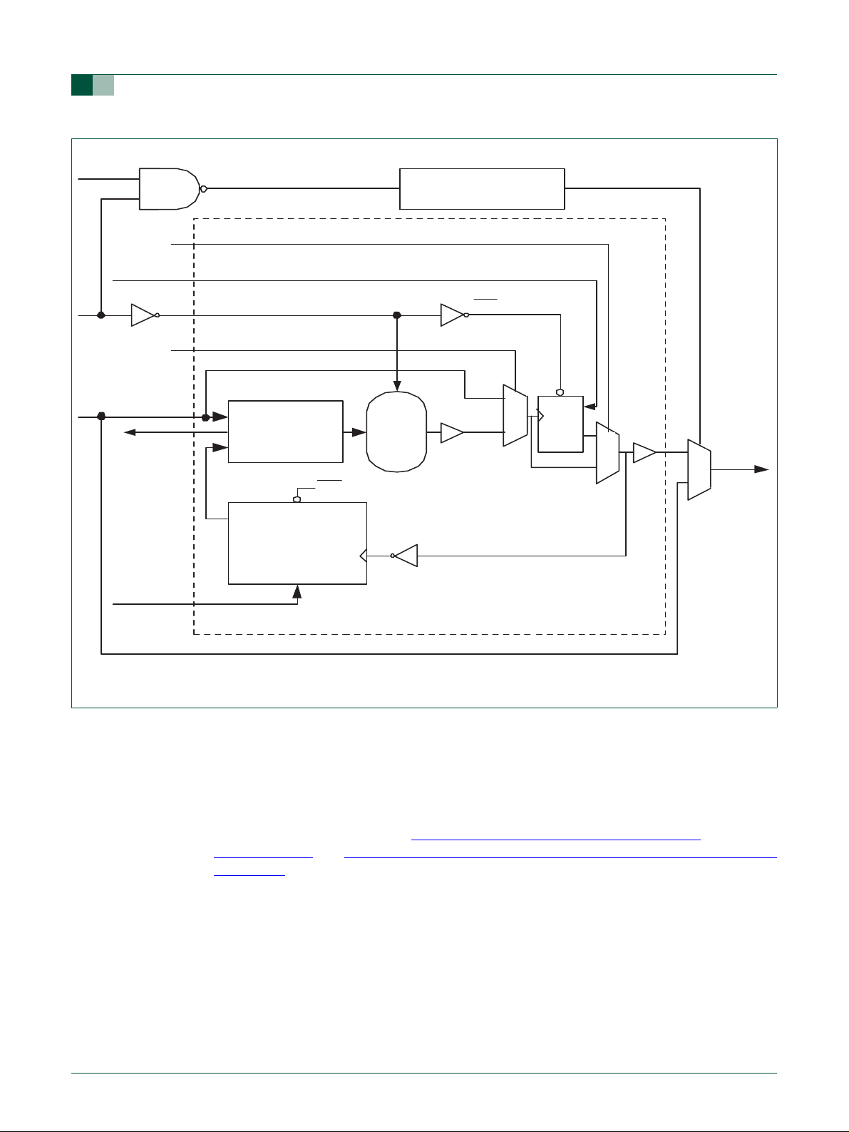
UM10120
PLLC
PLLE
F
OSC
PSEL[1:0]
PLOCK
MSEL[4:0]
CLOCK
SYNCHRONIZATION
Direct
0
PD
Bypass
0
PHASE-
FREQUENCY
DETECTOR
F
OUT
CD
DIV-BY-M
MSEL<4:0>
PD
CCO
PD
1
CD
F
CCO
0
/2P
0
0
1
CCLK
1
Fig 10. PLL block diagram
3.7.2 PLL Control register (PLLCON - 0xE01F C080)
The PLLCON register contains the bits that enable and connect the PLL. Enabling the
PLL allows it to attempt to lock to the current settings of the multiplier and divider values.
Connecting the PLL causes the processor and all chip functions to run from the PLL
output clock. Changes to the PLLCON register do not take effect until a correct PLL feed
sequence has been given (see
0xE01F C08C)” and Section 3.7.3 “PLL Configuration register (PLLCFG - 0xE01F C084)”
on page 29).
© Koninklijke Philips Electronics N.V. 2005. All rights reserved.
User manual Rev. 01 — 24 June 2005 28
Section 3.7.7 “PLL Feed register (PLLFEED -

Philips Semiconductors
Volume 1 Chapter 3: System Control Block
Table 14: PLL Control register (PLLCON - address 0xE01F C080) bit description
Bit Symbol Description Reset
0 PLLE PLL Enable. When one, and after a valid PLL feed, this bit will
1 PLLC PLL Connect. When PLLC and PLLE are both set to one, and after a
7:2 - Reserved, user software should not write ones to reserved bits. The
The PLL must be set up, enabled, and Lock established before it may be used as a clock
source. When switching from the oscillator clock to the PLL output or vice versa, internal
circuitry synchronizes the operation in order to ensure that glitches are not generated.
Hardware does not insure that the PLL is loc ked before it is connected or automatically
disconnect the PLL if lock is lost during operation. In the event of loss of PLL lock, it is
likely that the oscillator clock has become unstable and disconnecting the PLL will not
remedy the situation.
UM10120
activate the PLL and allow it to lock to the requested frequency. See
PLLSTAT register,
valid PLL feed, connects the PLL as the clock source for the
microcontroller. Otherwise, the oscillator clock is used directly by the
microcontroller. See PLLSTAT register,
value read from a reserved bit is not defined.
Table 16.
Table 16.
value
0
0
NA
3.7.3 PLL Configuration register (PLLCFG - 0xE01F C084)
The PLLCFG register contains the PLL multiplier and divider values. Changes to the
PLLCFG register do not take effect until a correct PLL feed sequence has been given (see
Section 3.7.7 “PLL Feed register (PLLFEED - 0xE01F C08C)” on page 30). Calculations
for the PLL frequency, and multiplier and divider values are found in the PLL Frequency
Calculation section on
Table 15: PLL Configuration register (PLLCFG - address 0xE01F C084) bit description
Bit Symbol Description Reset
4:0 MSEL PLL Multipl ier value. Supplies the value "M" in the PLL frequency
6:5 PSEL PLL Divider value. Supplies the value "P" in the PLL frequency
7 - Reserved, user software should not write ones to reserved bits. The
page 31.
calculations.
Note: For details on selecting the right value for MSEL see Section
3.7.9 “PLL frequency calculation” on page 31.
calculations.
Note: For details on selecting the right value for PSEL see Section
3.7.9 “PLL frequency calculation” on page 31.
value read from a reserved bit is not defined.
3.7.4 PLL Status register (PLLSTA T - 0xE01F C088)
value
0
0
NA
The read-only PLLSTAT register provides the actual PLL parameters that are in effect at
the time it is read, as well as the PLL status. PLLSTAT may disagree with values found in
PLLCON and PLLCFG because changes to those registers do not take effect until a
proper PLL feed has occurred (see
0xE01F C08C)”).
© Koninklijke Philips Electronics N.V. 2005. All rights reserved.
User manual Rev. 01 — 24 June 2005 29
Section 3.7.7 “PLL Feed register (PLLFEED -

Philips Semiconductors
Volume 1 Chapter 3: System Control Block
Table 16: PLL Status register (PLLSTAT - address 0xE01F C088) bit description
Bit Symbol Description Reset
4:0 MSEL Read-back for the PLL Multiplier value. This is the value currently
6:5 PSEL Read-back for the PLL Divider value. This is the value currently
7 - Reserved, user software should not write ones to reserved bits.
8 PLLE Read-back for the PLL Enable bit. When one, the PLL is currently
9 PLLC Read-back for the PLL Connect bit. When PLLC and PLLE are both
10 PLOCK Reflects the PLL Lock status. When zero, the PLL is not locked.
15:11 - Reserved, user software should not write ones to reserved bits.
UM10120
value
0
used by the PLL.
0
used by the PLL.
NA
The value read from a reserved bit is not defined.
0
activated. When zero, the PLL is turned off. This bit is automatically
cleared when Power-down mode is activated.
0
one, the PLL is connected as the clock source for the
microcontroller. When either PLLC or PLLE is zero, the PLL is
bypassed and the oscillator clock is used directly by the
microcontroller. This bit is automatically cleared when Power-down
mode is activated.
0
When one, the PLL is locked onto the requested frequency.
NA
The value read from a reserved bit is not defined.
3.7.5 PLL Interrupt
The PLOCK bit in the PLLSTA T register is connected t o the interrupt controller . This allo ws
for software to turn on the PLL and continue wit h other function s without ha ving t o wait f or
the PLL to achieve lock. When the interrupt occurs (PLOCK
connected, and the interrupt disabled.
3.7.6 PLL Modes
The combinations of PLLE and PLLC are shown in Table 17.
Table 17: PLL Control bit combinations
PLLC PLLE PLL Function
0 0 PLL is turned off and disconnected. The system runs from the unmodified clock
input.
0 1 The PLL is active, but not yet connected. The PLL can be connected after
PLOCK is asserted.
1 0 Same as 00 combination. This prevents the possibility of the PLL being
connected without also being enabled.
1 1 The PLL is active and has been connected as the system clock source.
3.7.7 PLL Feed register (PLLFEED - 0xE01F C08C)
A correct feed sequence must be written to the PLLFEED register in order for changes to
the PLLCON and PLLCFG registers to take effect. The feed sequence is:
= 1), the PLL may be
1. Write the value 0xAA to PLLFEED.
2. Write the value 0x55 to PLLFEED.
© Koninklijke Philips Electronics N.V. 2005. All rights reserved.
User manual Rev. 01 — 24 June 2005 30

Philips Semiconductors
Volume 1 Chapter 3: System Control Block
The two writes must be in the correct sequence, and must be consecutive VPB bus
cycles. The latter requirement implies that interr u p ts must be disabled for the duration of
the PLL feed operation. If either of the feed values is incorrect, or one of the previously
mentioned conditions is not met, any changes to the PL LCON or PLLCFG regist er will not
become effective.
Table 18: PLL Feed register (PLLFEED - address 0xE01F C08C) bit description
Bit Symbol Description Reset
7:0 PLLFEED The PLL feed sequence must be written to this register in order for
3.7.8 PLL and Power-down mode
Power-down mode automatically turns off and disconnects the PLL. Wakeup from
Power-down mode does not automatically restore the PLL settings, this must be done in
software. Typically, a routine to activate the PLL, wait for lock, and then connect the PLL
can be called at the beginning of any interrupt service routine that might be called due to
the wakeup. It is important not to attempt to restart the PLL by simply feeding it when
execution resumes after a wakeup from Power-down mode. This would enable and
connect the PLL at the same time, before PLL lock is established.
UM10120
value
0x00
PLL configuration and control register changes to take effect.
3.7.9 PLL frequency calculation
The PLL equations use the following parameters:
CCO
= F
Table 19: Elemens determining PLL’s frequency
Element Description
F
OSC
F
CCO
CCLK the PLL output frequency (also the processor clock frequency)
M PLL Multiplier value from the MSEL bits in the PLLCFG register
P PLL Divider value from the PSEL bits in the PLLCFG register
The PLL output frequency (when the PLL is both active and connected) is given by:
CCLK = M × F
The CCO frequency can be computed as:
F
= CCLK × 2 × P or F
CCO
The PLL inputs and settings must meet the following:
the frequency from the crystal oscillator/external osicillator
the frequency of the PLL current controlled oscillator
or CCLK = F
OSC
CCO
OSC
/ (2 × P)
× M × 2 × P
• F
• CCLK is in the range of 10 MHz to F
• F
© Koninklijke Philips Electronics N.V. 2005. All rights reserved.
User manual Rev. 01 — 24 June 2005 31
is in the range of 10 MHz to 25 MHz.
OSC
(the maximum allowed frequency for the
max
microcontroller - determined by the system microcontroller is embedded in).
is in the range of 156 MHz to 320 MHz.
CCO

Philips Semiconductors
Volume 1 Chapter 3: System Control Block
3.7.10 Procedure f or detrmining PLL settings
If a particular application uses the PLL, its configuration may be determined as follows:
1. Choose the desired processor operating frequency (CCLK). This may be based on
processor throughput requirements, need to support a specific set of UART baud
rates, etc. Bear in mind that peripheral devices may be running from a lower clock
than the processor (see
2. Choose an oscillator frequency (F
multiple of F
3. Calculate the value of M to configure the MSEL bits. M = CCLK / F
the range of 1 to 32. The value written to the MSEL bits in PLLCFG is M − 1 (see
Table 21.
4. Find a value for P to configure the PSEL bits, such that F
frequency limits. F
of the values 1, 2, 4, or 8. The value written to the PSEL bits in PLLCFG is 00 for
P
= 1; 01 for P = 2; 10 for P = 4; 11 for P = 8 (see Table 20).
Table 20: PLL Divider values
PSEL Bits (PLLCFG bits [6:5]) Value of P
00 1
01 2
10 4
11 8
OSC
UM10120
Section 3.10 “VPB divider” on page 38).
). CCLK must be the whole (non-fractional)
OSC
.
. M must be in
OSC
is within its defined
CCO
is calculated using the equation given above. P must h ave one
CCO
Table 21: PLL Multiplier values
MSEL Bits (PLLCFG bits [4:0]) Value of M
00000 1
00001 2
00010 3
00011 4
... ...
11110 31
11111 32
3.7.11 PLL example
System design asks for F
Based on these specifications, M = CCLK / Fosc = 60 MHz / 10 MHz = 6. Consequently,
M
- 1 = 5 will be written as PLLCFG[4:0].
V alue f or P can be deriv ed from P = F
in range of 156
F
= 156 MHz, P = 156 MHz / (2 x 60 MHz) = 1.3. The highest F
CCO
produces P
listed in
= 2.67. The only solution for P that satisf ies both of th ese requir ements and is
Table 20 is P = 2. Therefore, PLLCFG[6:5] = 1 will be used.
= 10 MHz and requires CCLK = 60 MHz.
OSC
/ (CCLK x 2), using condition that F
CCO
MHz to 320 MHz. Assuming the lowest allowed frequency for
frequency criteria
CCO
must be
CCO
© Koninklijke Philips Electronics N.V. 2005. All rights reserved.
User manual Rev. 01 — 24 June 2005 32

Philips Semiconductors
Volume 1 Chapter 3: System Control Block
3.8 Power control
The LPC2131/2/4/6/8 supports two reduced power modes: Idle mode and Power-down
mode. In Idle mode, e x ecution of inst ructions is suspended until either a Reset or inter rupt
occurs. Peripheral functions continue operation during Idle mode and may generate
interrupts to cause the processor to resume execution. Idle mode eliminates power used
by the processor itself, memory systems and related controllers, and inte rnal buses.
In Power-down mode, the oscillator is shut down and the chip receives no internal clocks.
The processor state and registers, peripheral registers, and internal SRAM values are
preserved throughout Power-down mode and the logic levels of chip pins remain static.
The Power-down mode can be terminated and normal operation resumed by either a
Reset or certain specific interrupts that are able to function without clocks. Since all
dynamic operation of the chip is suspended, Power-down mode reduces chip power
consumption to nearly zero.
Entry to Power-down and Idle modes must be coordinated with program execution.
Wakeup from Power-down or Idle modes via an interrupt resumes program execution in
such a way that no instructions are lost, incomplete, or repeated. Wake up from
Po wer-down mode is discussed further in
UM10120
Section 3.11 “Wakeup timer” on page 39.
A Power Control for Peripherals feature allows individual peripherals to be turned off if
they are not needed in the application, resulting in additional power savings.
3.8.1 Register description
The Power Control function contains two registers, as shown in Table 22. More detailed
descriptions follow.
Table 22: Power control registers
Name Description Access Reset
PCON Power Control Register. This register contains
control bits that enable the two reduced power
operating modes of the microcontroller. See
Table 23.
PCONP Power Control for Peripherals Register. This
register contains control bits that enable and
disable individual peripheral functions,
Allowing elimination of power consumption by
peripherals that are not needed.
[1] Reset value relects the data stored in used bits only. It does not include reserved bits content.
3.8.2 Power Control register (PCON - 0xE01F COCO)
The PCON register contains two bits. Writing a one to the corresponding bit causes entry
to either the Power-down or Idle mode. If both bits are set, Power-down mode is entered.
R/W 0x00 0xE01F C0C0
R/W 0x0018 17BE 0xE01F C0C4
value
[1]
Address
© Koninklijke Philips Electronics N.V. 2005. All rights reserved.
User manual Rev. 01 — 24 June 2005 33

Philips Semiconductors
Volume 1 Chapter 3: System Control Block
Table 23: Power Control register (PCON - address 0xE01F COCO) bit description
Bit Symbol Description Reset
0 IDL Idle mode - when 1, this bit causes the processor clock to be stopped,
1 PD Power-down mode - when 1, this bit causes the oscillator and all
2 PDBOD When PD is 1 and this bit is 0, Brown Out Detection remains operative
7:3 - Reserved, user software should not write ones to reserved bits. The
[1] Since execution is delayed until after the Wakeup Timer has allowed the main oscillator to resume stable
operation, there is no guarantee that execution will resume before V
threshhold, which prevents execution. If execution does resume, there is no guarantee of how long the
microcontroller will continue execution bef ore the low er BOD threshhold terminates execution. These issues
depend on the slope of the decline of V
vicinity of the microcontroller will improve the likelihood that software will be able to do what needs to be
done when power is being lost.
UM10120
while on-chip peripherals remain active. Any enabled interrupt from a
peripheral or an external interrupt source will cause the processor to
resume execution.
on-chip clocks to be stopped. A wakeup condition from an external
interrupt can cause the oscillator to restart, the PD bit to be cleared,
and the processor to resume execution.
during Power-down mode, such that its Reset can release the
microcontroller from Power-down mode
both 1, the BOD circuit is disabled during Power-down mode to
conserve power. When PD is 0, the state of this bit has no effect.
value read from a reserved bit is not defined.
. High decoupling capacitance (between VDD and ground) in the
DD
[1]
. When PD and this bit are
has fallen below the lower BOD
DD
value
0
0
0
NA
3.8.3 Power Control for Peripherals register (PCONP - 0xE01F COC4)
The PCONP register allows turning off selected peripheral functions for the purpose of
saving power. This is accomplished by gating off the clock source to the specified
peripheral blocks . A f ew p eripheral functions cannot b e turned off (i.e. the W at chdog timer,
GPIO, the Pin Conn ect block, and the System Control block). Some peripherals,
particularly those that include analog functions, may consume power that is not clock
dependent. These peripherals may contain a separate disable control that turns off
additional circuitry to reduce power. Each bit in PCONP controls one of the peripherals.
The bit numbers correspond to the related peripheral number as shown in the VPB
peripheral map
Figure 5 “VPB peripheral map” in the "LPC2131/2/4/6/8 Memory
Addressing" chapter.
If a peripheral control bit is 1, that peripheral is enabled. If a peripheral bit is 0, that
peripheral is disabled to conserve power. For example if bit 19 is 1, the I
enabled. If bit 19 is 0, the I
2
C1 interface is disabled.
2
C1 interface is
Important: valid read from a peripheral register and valid write to a peripheral
register is possible only if that peripheral is enabled in the PCONP register!
© Koninklijke Philips Electronics N.V. 2005. All rights reserved.
User manual Rev. 01 — 24 June 2005 34

Philips Semiconductors
Volume 1 Chapter 3: System Control Block
Table 24: Power Control for Peripherals register (PCONP - address 0xE01F C0C4) bit
Bit Symbol Description Reset
0 - Reserved, user software should not write ones to reserved bits. The
1 PCTIM0 Timer/Counter 0 power/clock control bit. 1
2 PCTIM1 Timer/Counter 1 power/clock control bit. 1
3 PCUART0 UART0 power/clock control bit. 1
4 PCUART1 UART1 power/clock control bit. 1
5 PCPWM0 PWM0 power/clock control bit. 1
6 - Reserved, user software should not write ones to reserved bits. The
7 PCI2C0 The I2C0 interface power/clock control bit. 1
8 PCSPI0 The SPI0 interface power/clock control bit. 1
9 PCRTC Th e RTC power/clock control bit. 1
10 PCSPI1 The SSP interface power/clock control bit. 1
11 - Reserved, user software should not write ones to reserved bits. The
12 PCAD0 A/D converter 0 (ADC0) power/clock control bit.
18:13 - Reserved, user software should not write ones to reserved bits. The
19 PCI2C1 The I2C1 interface power/clock control bit. 1
20 PCAD1 A/D converter 1 (ADC1) power/clock control bit.
31:21 - Reserved, user software should not write ones to reserved bits. The
description
value read from a reserved bit is not defined.
value read from a reserved bit is not defined.
value read from a reserved bit is not defined.
Note: Clear the PDN bit in the AD0CR before clearing this bit, and set
this bit before setting PDN.
value read from a reserved bit is not defined.
Note: Clear the PDN bit in the AD1CR before clearing this bit, and set
this bit before setting PDN.
value read from a reserved bit is not defined.
UM10120
value
NA
NA
NA
1
NA
1
NA
3.8.4 Power control usage notes
After every reset, the PCONP register contains the value that enables all interfaces and
peripherals controlled by the PCONP to be enabled. Therefore, apart from proper
configuring via peripheral dedicated registers, the user’s application has no need to
access the PCONP in order to start using any of the on-board peripherals.
Power saving oriented systems should have 1s in the PCONP register only in positi ons
that match peripherals really used in the application. All other bits, declared to be
"Reserved" or dedicated to the peripherals not used in the curr ent application, must be
cleared to 0.
3.9 Reset
Reset has two sources on the LPC2131/2/4/6/8: the RESET pin and Watchdog Reset.
The
RESET pin is a Schmitt trigger input pin with an additional glitch filter. Assertion of
chip Reset by any source starts the Wakeup Timer (see description in
© Koninklijke Philips Electronics N.V. 2005. All rights reserved.
User manual Rev. 01 — 24 June 2005 35
Section 3.11

Philips Semiconductors
Volume 1 Chapter 3: System Control Block
“Wakeup timer” in this chapter), causing reset to remain asserted until the external Reset
is de-asserted, the oscillator is running, a fixed number of clocks have passed, and the
on-chip circuitry has completed its initialization. The relationship between Reset, the
oscillator, and the Wakeup Timer are shown in
The Reset glitch filter allows the processor to ignore external reset pulses that are very
short, and also determines the minimum duration of
order to guarantee a chip reset. Once asserted,
crystal oscillator is fully running and an adequate signal is present on the X1 pin of the
microcontroller. Assuming that an external crystal is used in the crystal oscillator
subsystem, after power on, the
subsequent resets when crystal oscillator is already running and stable signal is on the X1
pin, the
When the internal Reset is removed, the processor begins executing at address 0, which
is initially the Reset vector mapped from the Boot Block. At that point, all of the processor
and peripheral registers have been initialized to predetermined values.
External and internal Resets have some small differences. An external Reset causes the
value of certain pins to be latched to configure the part. External circuitry cannot
determine when an internal Reset occurs in order to allow setting up those special pins,
so those latches are not reloaded during an internal Reset. Pins that are e x amined during
an external Reset for various purposes are: P1.20/TRACESYNC , P1.26/RTCK (see
chapters "Pin Configuration" on
(see "Flash Memory System and Programming" chapter on page 216) is examined by
on-chip bootloader when this code is executed after ev ery Reset.
UM10120
Figure 11.
RESET that must be asserted in
RESET pin can be deasserted only when
RESET pin should be asserted for 10 ms. For all
RESET pin needs to be asserted for 300 ns only.
page 64 and "Pin Connect Block" on page 73). Pin P0.14
It is possible for a chip Reset to occur during a Flash programming or erase operation.
The Flash memory will interrupt the ongoing operation and hold off the completion of
Reset to the CPU until internal Flash high voltages have settled.
© Koninklijke Philips Electronics N.V. 2005. All rights reserved.
User manual Rev. 01 — 24 June 2005 36

Philips Semiconductors
Volume 1 Chapter 3: System Control Block
UM10120
External
reset
Watchdog
reset
Power
down
EINT0 Wakeup
EINT1 Wakeup
EINT2 Wakeup
EINT3 Wakeup
RTC Wakeup
Reset to the
C
Q
S
Oscillator
output
(F
)
OSC
Write “1”
from VPB
on-chip
circuitry
Reset to
PCON.PD
WAKEUP TIMER
START
COUNT 2
Reset
n
C
Q
S
VBP Read
of PDBIT
in PCON
F
OSC
to PLL
Fig 11. Reset block diagram includ in g the w akeup timer
3.9.1 Reset Source Identification Register (RSIR - 0xE01F C180)
This register contains one bit for each source of Reset. Writing a 1 to any of these bits
clears the corresponding read-side bit to 0. The interactions among the four sources are
described below.
Table 25: Reset Source identificator Register (RSIR - address 0xE01F C180) bit description
Bit Symbol Description Reset
0 POR Assertion of the POR signal sets this bit, and clears all of the other bits
in this register. But if another Reset signal (e.g., External Reset) remains
asserted after the POR signal is negated, then its bit is set. This bit is not
affected by any of the other sources of Reset.
1 EXTR Assertion of the RESET signal sets this bit. Ths bit is cleared by POR,
but is not affected by WDT or BOD reset.
value
see text
see text
© Koninklijke Philips Electronics N.V. 2005. All rights reserved.
User manual Rev. 01 — 24 June 2005 37

Philips Semiconductors
Volume 1 Chapter 3: System Control Block
Table 25: Reset Source identificator Register (RSIR - address 0xE01F C180) bit description
Bit Symbol Description Reset
2 WDTR This bit is set when the Watchdog Timer times out and the WDTRESET
3 BODR This bit is set when the 3.3 V power reaches a level below 2.6 V. If the
7:4 - Reserved, user software should not write ones to reserved bits. The
3.10 VPB divider
The VPB Divider determines the relationship between the processor cloc k (CCLK) and the
clock used by peripheral devices (PCLK). The VPB Divider serves tw o purposes. The first
is to provides peripherals with desired PCLK via VPB bus so that they can operate at the
speed chosen for the ARM processor. In order to achieve this, the VPB bu s may be
slowed down to one half or one fourth of the processor clock rate. Because the VPB bus
must work properly at power up (and its timing cannot be altered if it does not work since
the VPB divider control registers reside on the VPB bus), the default condition at reset is
for the VPB bus to run at one quarter speed. The second purpose of the VPB Divider is to
allow power sa vings when an application does not re quire any peripheral s to run at the full
processor rate.
UM10120
bit in the Watchdog Mode Register is 1. It is cleared by any of the other
sources of Reset.
voltage dips fr om 3.3 V to 2.5 V and backs up, the BODR bit will be
V
DD
set to 1. Also, if the V
level above 2.6 V, the BODR will be set to 1, too. This bit is not affected
by External Reset nor Watchdog Reset.
Note: only in case a reset occurs and the POR = 0, the BODR bit
indicates if the VDD voltage was below 2.6 V or not.
value read from a reserved bit is not defined.
voltage rises continuously from below 1 V to a
DD
value
see text
seet text
NA
The connection of the VPB Divider relative to the oscillator and the processor clock is
shown in
remains active (if it was running) during Idle mode.
Figure 12. Because the VPB Divider is connected to the PLL output, the PLL
3.10.1 Register description
Only one register is used to control the VPB Divider.
Table 26: VPB divider register map
Name Description Access Reset
value
VPBDIV Controls the rate of the VPB clock in relation to
the processor clock.
[1] Reset value relects the data stored in used bits only. It does not include reserved bits content.
R/W 0x00 0xE01F C100
Address
[1]
3.10.2 VPBDIV register (VPBDIV - 0xE01F C100)
The VPB Divider register contains two bits, allowing three divider values, as shown in
Table 27.
© Koninklijke Philips Electronics N.V. 2005. All rights reserved.
User manual Rev. 01 — 24 June 2005 38

Philips Semiconductors
Volume 1 Chapter 3: System Control Block
Table 27: VPB Divider register (VPBDIV - address 0xE01F C100) bit description
Bit Symbol Value Description Reset
1:0 VPBDIV 00 VPB bus clock is one fourth of the processor clock. 00
7:2 - - Reserved, user software should not write ones to reserved
external clock source
01 VPB bus clock is the same as the processor clock.
10 VPB bus clock is one half of the processor clock.
11 Reserved. If this value is written to the VPBDIV register, it
Crystal oscillator
or
)
(F
OSC
UM10120
has no effect (the previous setting is retained).
bits. The value read from a reserved bit is not defined.
PLL
Processor clock
(CCLK)
value
NA
Fig 12. VPB divider connections
3.11 Wakeup timer
The purpose of the wakeup timer is to ensure that the oscillator and other analog
functions required for chip operation are fully functional before the processor is allowed to
execute instructions. This is important at power on, all types of Reset, and wh en ever any
of the aforementioned functions are turned off for any reason. Since the oscillator and
other functions are turn e d off during Power-down mode, any wakeup of the processor
from Power-down mode makes use of the Wakeup Timer.
The Wakeup Timer monitors the crystal oscillator as the means of checking whether it is
safe to begin code execution. When power is applied to the chip, or some event caused
the chip to exit Power-down mode, some time is required for the oscillator to produce a
signal of sufficient amplitude to drive the clock logic. The amount of time depends on
many factors, including the rate of V
and its electrical characteristics (if a quartz crystal is used), as well as any other external
circuitry (e.g. capacitors), and the characteristics of the oscillator itself under the existing
ambient conditions.
VPB
DIVIDER
ramp (in the case of power on), the type of crystal
DD
VPB Clock
(PCLK)
Once a clock is detected, the Wakeup Timer counts 4096 clocks, then enables the on-chip
circuitry to initialize. When the onboard m odules initialization is complete, the processor is
released to execute instructions if the external Reset has been deasserted. In the case
where an external clock source is used in the system (as opposed to a crystal connected
to the oscillator pins), the possibility that there could be little or no delay for oscillator
start-up must be considered. The Wakeup Timer design then ensures that any other
required chip functions will be operational prior to the beginning of program execution.
© Koninklijke Philips Electronics N.V. 2005. All rights reserved.
User manual Rev. 01 — 24 June 2005 39

Philips Semiconductors
Volume 1 Chapter 3: System Control Block
Any of the various Resets can bring the microcontroller out of power-down mode, as can
the external interrupts EINT3:0, plus the R TC interrupt if the R TC is operati ng from its o wn
oscillator on the RTCX1-2 pins. When one of these interrupts is enabled for wakeup and
its selected event occurs, an oscillator w akeup cycle is started. The actual interrupt (if any)
occurs after the wakeup timer expires, and is handled by the Vecto re d Int er rupt Contro ller.
However, the pin multiplexing on the LPC2131/2/4/6/8 (see chapters "Pin Conf iguration "
on
page 64 and "Pin Connect Block" on page 73) was designed to allow other peripherals
to, in effect, bring the device out of P ower-down mode. The following pin-function pairings
allow interrupts from events relating to UART0 or 1, SPI 0 or 1, or the I
SDA / EINT1, SSEL0 / EINT2, RxD1 / EINT3, DCD1 / EINT1, RI1 / EINT2, SSEL1 /
EINT3.
To put the device in Power-down mode and allo w activity on one or m ore of these b uses or
lines to power it back up, software should reprog r am the pin funct ion to Exte rnal Interrupt,
select the appropriate mode and polarity for the Interrupt, and then select Power-down
mode. Upon wakeup software should restore the pin multiplexing to the peripheral
function.
All of the bus- or line-activity indications in the list above happen to be low-active. If
software wants the device to come out of power -down mode in response to activity on
more than one pin that share the same EINTi channel, it should program low-level
sensitivity for that channel, because only in level mode will the channel logically OR the
signals to wake the device.
UM10120
2
C: RxD0 / EINT0,
The only flaw in this scheme is that the time to restart the oscillator prevents the
LPC2131/2/4/6/8 from capturing the bus or line activity that wak es it up . Idle mode is more
appropriate than power-do wn mode for devices that must capture and resp ond to e xt ernal
activity in a timely manner.
To summarize: on the LPC2131/2/4/6/8, the Wakeup Timer enforces a minimum reset
duration based on the crystal oscillator, and is activated whenever there is a wakeup from
Power-down mode or any type of Reset.
3.12 Brown-out detection
The LPC2131/2/4/6/8 includes 2-stage monitoring of the voltage on the VDD pins. If this
voltage fa lls be low 2.9
Vectored Interrupt Controller. This signal can be enabled for interrupt in the Interrupt
Enable register (see
0xFFFF F010)” on page 52); if not, software can monitor the signal by reading the Raw
Interrupt Status register (see Section 5.4.3 “Raw Interrupt status register (VICRawIntr -
0xFFFF F008)” on page 52).
The second stage of low-voltage detection asserts Reset to inactivate the
LPC2131/2/4/6/8 when the voltage on the V
alteration of the Flash as operation of the various elements of the chip would otherwise
become unreliable due to low voltage. The BOD circuit maintains this reset down below
1
V, at which point the Power-On Reset circuitry maintains the overall Reset.
V, the Brown-Out Detector (BOD) asserts an interrupt signal to the
Section 5.4.4 “Interrupt Enable register (VICIntEnable -
pins falls below 2.6 V. This Reset prevents
DD
Both the 2.9 V and 2.6 V thresholds include some hysteresis. In normal operation, this
hysteresis allows the 2.9
loop to sense the condition.
© Koninklijke Philips Electronics N.V. 2005. All rights reserved.
User manual Rev. 01 — 24 June 2005 40
V detection to reliably interrupt, or a regularly-executed event

Philips Semiconductors
Volume 1 Chapter 3: System Control Block
But when Brown-Out Detection is enabled to bring the LPC2131/2/4/6/8 out of
Pow er-Do wn mode (which is itself not a guar antee d operat ion -- see
Control register (PCON - 0xE01F COCO)”), the supply voltage may recover from a
transient before the Wakeup Timer has completed its delay. In this case, the net result of
the transient BOD is that the part wakes up a nd continues operation after the instructions
that set Power-Down Mode, without any interrupt occurring and with the BOD bit in the
RISR being 0. Since all other wakeu p conditions have latching flags (see
“External Interrupt Flag register (EXTINT - 0xE01F C140)” and Section 18.4.3 “Interrupt
Location Register (ILR - 0xE002 4000)” on page 202), a wakeup of this type, without any
apparent cause, can be assumed to be a Brown-Out that has gone away.
3.13 Code security vs debugging
Applications in development typically need the deb ugging and tracing facilities in the
LPC2131/2/4/6/8. Later in the life cycle of an application, it may be more important to
protect the application code from observation b y hostile or competitiv e e y es. Th e f ollowing
feature of the LPC2131/2/4/6/8 allows an application to control whether it can be
debugged or protected from observation.
UM10120
Section 3.8.2 “Power
Section 3.5.2
Details on the way Code Read Protection works can be found in the "Flash Memory
System and Programming" chapter on
page 216.
© Koninklijke Philips Electronics N.V. 2005. All rights reserved.
User manual Rev. 01 — 24 June 2005 41

4.1 Introduction
4.2 Operation
UM10120
Chapter 4: Memory Acceleration Module (MAM)
Rev. 01 — 24 June 2005 User manual
The MAM block in the LPC2131/2/4/6/8 maximizes the performance of the ARM
processor when it is running code in Flash memory, but does so using a single Flash
bank.
Simply put, the Memory Accelerator Module (MAM) attempts to have the next ARM
instruction that will be needed in its latches in time to prevent CPU fetch stalls. The
LPC2131/2/4/6/8 uses one bank of Flash memory, compared to the two banks used on
predecessor devices. It includes three 128-bit buffers called the Prefetch Buffer, the
Branch Trail Buffer and the data buffer . When an Instruction Fetch is not satisfied by either
the Prefetch or Bran ch Trail Buffer, nor has a prefetch been initiated for that line, the ARM
is stalled while a fetch is initiated for the 128-bit line . If a pref etch has been initiate d but not
yet completed, the ARM is stalled for a shorter time. Unless aborted by a data access, a
prefetch is initiated as soon as the Flash has completed the previous access. The
prefetched line is latched by the Flash module, but the MAM does not capture the line in
its prefetch buffer until the ARM core presents the address from which the prefetch has
been made. If the core presents a different address from the one from which the prefetch
has been made, the prefetched line is discarded.
The Prefetch and Branch Trail buffers each include four 32-bit ARM instructions or eight
16-bit Thumb instructions. During sequential code execution, typically the Prefetch Buffer
contains the current instruction and the entire Flash line that contains it.
The MAM uses the LPROT[0] line to differentiate between instruction and data accesses.
Code and data accesses use separat e 128-bit buffers. 3 of e very 4 sequential 32-bit code
or data accesses "hit" in the buffer without requiring a Flash access (7 of 8 sequential
16-bit accesses, 15 of every 16 sequential byte accesses). The fourth (eighth, 16th)
sequential data access must access Flash, aborting any prefetch in progress. When a
Flash data access is concluded, any prefetch that had been in progress is re-initiated.
Timing of Flash read operations is programmable and is described later in this section.
In this manner , there is no code f etch penalty f or sequenti al instruction ex ecution when the
CPU clock period is greater than or equal to one fourth of the Flash access time. The
average amount of time spent doing program branches is relatively small (less than 25%)
and may be minimized in ARM (rather than Thumb) code through the use of the
conditional execution feature present in all ARM instructions. This conditional execution
may often be used to a void small forward branches that wo uld otherwise be necessary.
Branches and other program flow changes cause a break in the sequential flow of
instruction fetches described above. The Branch Trail Buffer captures the line to which
such a non-sequential break occurs. If the same branch is taken again, the next
instruction is taken from the Branch Trail Buffer. When a branch outside the contents of
© Koninklijke Philips Electronics N.V. 2005. All rights reserved.
User manual Rev. 01 — 24 June 2005 42

Philips Semiconductors
Volume 1 Chapter 4: MAM Module
the Prefetch and Bra nch Trail Buffer is take n, a stall of se v eral clocks is needed to loa d the
Branch Trail buffer. Subsequently, there will typically be no further instructionfetch delays
until a new and different branch occurs.
4.3 MAM blocks
The Memory Accelerator Module is divided into several functional blocks:
• A Flash Address Latch and an incrementor function to form prefetch addresses
• A 128-bit Prefetch Bu ffer and an associated Address latch and comparator
• A 128-bit Branch Trail Buffer and an associated Address latch and comparat or
• A 128-bit Data Buffer and an associated Address latch and comparator
• Control logic
• Wait logic
Figure 13 shows a simplified bloc k diag ram of the Memory Accelerator Module da ta paths .
In the following descriptions , the term “f etch” applies to an e xplicit Fla sh read request from
the ARM. “Pre-fetch” is used to denote a Flash read of instructions beyond the current
processor fetch address.
UM10120
4.3.1 Flash memory bank
There is one bank of Flash memory with the LPC2131/2/4/6/8 MAM.
Flash programming operations are not controlled by the MAM, but are handled as a
separate function. A “boot block” sector contains Flash programming algorithms that may
be called as part of the application program, and a loader that may be run to allow serial
programming of the Flash memory.
ARM Local Bus
Memory Address
Flash Memory
Bank
BUS
INTERFACE
BUFFERS
Memory Data
Fig 13. Simplified block diagram of the Memory Accelerator Module (MAM)
© Koninklijke Philips Electronics N.V. 2005. All rights reserved.
User manual Rev. 01 — 24 June 2005 43

Philips Semiconductors
Volume 1 Chapter 4: MAM Module
4.3.2 Instruction latches and data latches
Code and Data accesses are treated separately by the Memory Accelerator Module.
There is a 128-bit Latch, a 15-bit Address
Latch, and a 15-bit comparator associated with each buffer (prefetch, branch trail, and
data). Each 128-bit latch holds 4 words (4 ARM instructions, or 8 Thumb instructions).
Also associated with each buffer are 32 4:1 Multiplexers that select the requested word
from the 128-bit line.
Each Data access that is not in the Data latch causes a Flash fetch of 4 words of data,
which are captured in the Data latch. This speeds up sequential Data operations, but has
little or no effect on random accesses.
4.3.3 Flash programming Issues
Since the Flash memory does not allow accesses during programming and erase
operations, it is necessary for the MAM to force the CPU to wait if a memory access to a
Flash address is requested while the Flash module is busy. (This is accomplished by
asserting the ARM7TDMI-S local bus signal CLKEN.) Under some conditions, this delay
could result in a Watchdog time-out. The user will need to be aware of this possibility and
take steps to insure that an unwanted Watchdog reset does not cause a system failure
while programming or erasing the Flash memory.
UM10120
In order to preclude the possibility of stale data being read from the Flash memory, the
LPC2131/2/4/6/8 MAM holding latches are automatically invalidated at the beginning of
any Flash programming or erase operation. Any subsequent read from a Flash address
will cause a new fetch to be initiated after the Flash operation has completed.
4.4 MAM operating modes
Three modes of operation are defined for the MAM, trading off perf ormance for ease of
predictability:
Mode 0: MAM off. All memory requests result in a Flash read operat ion (see note 2
below). There are no instruction prefetches.
Mode 1: MAM partially enabled. Sequential instruction accesses are fulfilled from the
holding latches if the data is present. Instruction prefetch is enabled. Non-sequential
instruction accesses initiate Flash read operations (see note 2 below). This means that
all branches cause memory fetches. All data oper ations cause a Flash read because
buffer ed data access timing is hard to predict and is very situation dependent.
Mode 2: MAM fully enabled. An y memory request (code or data) for a value that is
contained in one of the corresponding holding latches is fulfilled from the latch.
Instruction prefetch is enabled. Flash read operations are initiated for instruction
prefetch and code or data values not available in the corresponding holding latches.
© Koninklijke Philips Electronics N.V. 2005. All rights reserved.
User manual Rev. 01 — 24 June 2005 44

Philips Semiconductors
Volume 1 Chapter 4: MAM Module
Table 28: MAM Responses to program accesses of various types
Program Memory Request Type MAM Mode
Sequential access, data in latches Initiate Fetch
Sequential access, data not in latches Initiate Fetch Initiate Fetch
Non-sequential access, data in latches Initiate Fetch
Non-sequential access, data not in latches Initiate Fetch Initiate Fetch
[1] Instruction prefetch is enabled in modes 1 and 2.
[2] The MAM actually uses latched data if it is available, but mimics the timing of a Flash read operation. This
saves power while resulting in the same execution timing. The MAM can truly be turned off by setting the
fetch timing value in MAMTIM to one clock.
Table 29: MAM responses to data and DMA accesses of various types
Data Memory Request Type MAM Mode
Sequential access, data in latches Initiate Fetch
Sequential access, data not in latches Initiate Fetch Initiate Fetch Initiate Fetch
Non-sequential access, data in latches Initiate Fetch
Non-sequential access, data not in latches Initiate Fetch Initiate Fetch Initiate Fetch
UM10120
0 1 2
[2]
Use Latched
[1]
Data
[1]
[2]
Initiate Fetch
0 1 2
[1]
Initiate Fetch
[1]
Initiate Fetch
[1][2]
[1]
[1]
[1]
Use Latched
[1]
Data
Initiate Fetch
Use Latched
[1]
Data
Initiate Fetch
Use Latched
Data
Use Latched
Data
[1]
[1]
[1] The MAM actually uses latched data if it is available, but mimics the timing of a Flash read operation. This
saves power while resulting in the same execution timing. The MAM can truly be turned off by setting the
fetch timing value in MAMTIM to one clock.
4.5 MAM configuration
After reset the MAM defaults to the disabled state. Software can turn memory access
acceleration on or off at any time. This allows most of an application to be run at the
highest possible performance, while certain functions can be run at a somewhat slower
but more predictable rate if more precise timing is required.
4.6 Register description
All registers, regardless of size, are on word address boundaries. Details of the registers
appear in the description of each function.
© Koninklijke Philips Electronics N.V. 2005. All rights reserved.
User manual Rev. 01 — 24 June 2005 45

Philips Semiconductors
Volume 1 Chapter 4: MAM Module
Table 30: Summary of MAM registers
Name Description Access Reset
MAMCR Memory Accelerator Module Control Register.
Determines the MAM functional mode, that is, to
what extent the MAM performance enhancements
are enabled. See
MAMTIM Memory Accelerator Module Timing control.
Determines the number of clocks used for Flash
memory fetches (1 to 7 processor clocks).
[1] Reset value reflects the data stored in used bits only. It does not include reserved bits content.
Table 31.
4.7 MAM Control Register (MAMCR - 0xE01F C000)
Two configuration bits select the three MAM operating modes, as shown in Table 31.
Following Rese t, MAM functions ar e disable d. Changing the MAM op erating mode causes
the MAM to invalidate all of the holding latche s, resulti ng in new r eads of Flash inf ormation
as required.
UM10120
Address
[1]
value
R/W 0x0 0xE01F C000
R/W 0x07 0xE01F C004
Table 31: MAM Control Register (MAMCR - address 0xE01F C000) bit description
Bit Symbol Value Description Reset
1:0 MAM_mode
_control
7:2 - - Reserved, user software should not write ones to reserved
00 MAM functions disabled 0
01 MAM functions partially enabled
10 MAM functions fully enabled
11 Reserved. Not to be used in the application.
bits. The value read from a reserved bit is not defined.
4.8 MAM Timing register (MAMTIM - 0xE01F C004)
The MAM Timing register determines how many CCLK cycles are used to access the
Flash memory. This allows tuning MAM timing to match the processor operating
frequency. Flash access times from 1 clock to 7 clocks are possible. Single clock Flash
accesses would essentially remov e the MAM from timing calculations. In this case the
MAM mode may be selected to optimize power usage.
Table 32: MAM Timing register (MAMTIM - address 0xE01F C004) bit description
Bit Symbol Value Description Reset
2:0 MAM_fetch_
cycle_timing
000 0 - Reserved. 07
001 1 - MAM fetch cycles are 1 processor clock (CCLK) in
duration
010 2 - MAM fetch cycles are 2 CCLKs in duration
011 3 - MAM fetch cycles are 3 CCLKs in duration
100 4 - MAM fetch cycles are 4 CCLKs in duration
101 5 - MAM fetch cycles are 5 CCLKs in duration
value
NA
value
© Koninklijke Philips Electronics N.V. 2005. All rights reserved.
User manual Rev. 01 — 24 June 2005 46

Philips Semiconductors
Volume 1 Chapter 4: MAM Module
Table 32: MAM Timing register (MAMTIM - address 0xE01F C004) bit description
Bit Symbol Value Description Reset
7:3 - - Reserved, user software should not write ones to reserved
4.9 MAM usage notes
When changing MAM timing, the MAM must first be turned off by writing a zero to
MAMCR. A new value may then be written to MAMTIM. Finally, the MAM may be turned
on again by writing a value (1 or 2) corresponding to the desired operating mode to
MAMCR.
UM10120
value
110 6 - MAM fetch cycles are 6 CCLKs in duration
111 7 - MAM fetch cycles are 7 CCLKs in duration
Warning: These bits set the duration of MAM Flash fetch operations
as listed here. Improper setting of this value may result in incorrect
operation of the device.
NA
bits. The value read from a reserved bit is not defined.
For system clock slower than 20 MHz, MAMTIM can be 001. For system clock between
20
MHz and 40 MHz, Flash access time is suggested to be 2 CCLKs, while in systems
with system clock faster than 40
MHz, 3 CCLKs are proposed.
© Koninklijke Philips Electronics N.V. 2005. All rights reserved.
User manual Rev. 01 — 24 June 2005 47

5.1 Features
5.2 Description
UM10120
Chapter 5: Vectored Interrupt Controller (VIC)
Rev. 01 — 24 June 2005 User manual
• ARM PrimeCell™ Vectored Interrupt Controller
• 32 interrupt request inputs
• 16 vectored IRQ interrupts
• 16 priority levels dynamically assigned to interrupt requests
• Software interrupt generation
The Vectored Interrupt Controller (VIC) takes 32 interrupt request inputs and
programmably assigns the m into 3 cat egories , FIQ, vectored IRQ, and non-vectored IRQ.
The programmable assignment scheme means that priorities of interrupts from the
various peripherals can be dynamically assigned and adjusted.
Fast Inter rupt reQuest (FIQ) requests hav e the hig hest priority. If more than one request is
assigned to FIQ, the VIC ORs the requests to produce the FIQ signal to the ARM
processor. The fastest possible FIQ latency is achieved when only one request is
classified as FIQ, because then the FIQ service routine can simply start dealing with that
device. But if more than one request is assigned to the FIQ class, the FIQ service routine
can read a word from the VIC that identifies which FIQ source(s) is (are) requesting an
interrupt.
Vectored IRQs have the middle priority, but only 16 of the 32 requests can be assigned to
this category. Any of the 32 requests can be assigned to an y of the 16 v ectored I RQ slots ,
among which slot 0 has the highest priority and slot 15 has the lowest.
Non-vectored IRQs have the lowest priority.
The VIC ORs the requests from all the vectored and non-vectored IRQs to produce the
IRQ signal to the ARM processor. The IRQ service routine can start by reading a register
from the VIC and jumping there. If any of the vectored IRQs are requesting, the VIC
provides the address of the highest-priority requesting IRQs service routine, otherwise it
provides the address of a default routine that is shared by all the non-vectored IRQs. The
default routine can read another VIC register to see what IRQs are active.
All registers in the VIC are word registers. Byte and halfword reads and write are not
supported.
Additional information on the Vectored Interrupt Controller is available in the ARM
PrimeCell™ Vectored Interrupt Controller (PL190) documentation.
5.3 Register description
The VIC implements the registers shown in Table 33. More detailed descriptions follo w.
© Koninklijke Philips Electronics N.V. 2005. All rights reserved.
User manual Rev. 01 — 24 June 2005 48

Philips Semiconductors
UM10120
Volume 1 Chapter 5: VIC
Table 33: VIC register map
Name Description Access Reset
value
VICIRQStatus IRQ Status Register. This register reads out the state of
those interrupt requests that are enabled and classified as
IRQ.
VICFIQStatus FIQ Status Requests. This register reads out the state of
those interrupt requests that are enabled and classified as
FIQ.
VICRawIntr Raw Interrupt Status Register. This register reads out the
state of the 32 interrupt requests / software interrupts,
regardless of enabling or classification.
VICIntSelect Interrupt Select Register. This register classifies each of the
32 interrupt requests as contributing to FIQ or IRQ.
VICIntEnable Interrupt Enable Register. This register controls which of the
32 interrupt requests and software interrupts are enabled to
contribute to FIQ or IRQ.
VICIntEnClr Interrupt Enable Clear Register. This register allows
software to clear one or more bits in the Interrupt Enable
register.
VICSoftInt Software Interrupt Register. The conten ts of this reg ister are
ORed with the 32 interrupt requests from various peripheral
functions.
VICSoftIntClear Software Interrupt Clear Register. This register allows
software to clear one or more bits in the Software Interrupt
register.
VICProtection Protection enable register. This register allows limiting
access to the VIC registers by software running in privileged
mode.
VICVectAddr Vector Address Register. When an IRQ interrupt occurs, the
IRQ service routine can read this register and jump to the
value read.
VICDefVectAddr Default Vector Address Register. This register holds the
address of the Interrupt Service routin e (ISR) for
non-vectored IRQs.
VICVectAddr0 Vector address 0 register. Vector Address Registers 0-15
hold the addresses of the Interrupt Service routines (ISRs)
for the 16 vectored IRQ slots.
VICVectAddr1 Vector address 1 register. R/W 0 0xFFFF F104
VICVectAddr2 Vector address 2 register. R/W 0 0xFFFF F108
VICVectAddr3 Vector address 3 register. R/W 0 0xFFFF F10C
VICVectAddr4 Vector address 4 register. R/W 0 0xFFFF F110
VICVectAddr5 Vector address 5 register. R/W 0 0xFFFF F114
VICVectAddr6 Vector address 6 register. R/W 0 0xFFFF F118
VICVectAddr7 Vector address 7 register. R/W 0 0xFFFF F11C
VICVectAddr8 Vector address 8 register. R/W 0 0xFFFF F120
VICVectAddr9 Vector address 9 register. R/W 0 0xFFFF F124
VICVectAddr10 Vector address 10 register. R/W 0 0xFFFF F128
VICVectAddr11 Vector address 11 register. R/W 0 0xFFFF F12C
RO 0 0xFFFF F000
RO 0 0xFFFF F004
RO 0 0xFFFF F008
R/W 0 0xFFFF F00C
R/W 0 0xFFFF F010
WO 0 0xFFFF F014
R/W 0 0xFFFF F018
WO 0 0xFFFF F01C
R/W 0 0xFFFF F020
R/W 0 0xFFFF F030
R/W 0 0xFFFF F034
R/W 0 0xFFFF F100
Address
[1]
© Koninklijke Philips Electronics N.V. 2005. All rights reserved.
User manual Rev. 01 — 24 June 2005 49

Philips Semiconductors
Volume 1 Chapter 5: VIC
Table 33: VIC register map
Name Description Access Reset
value
VICVectAddr12 Vector address 12 register. R/W 0 0xFFFF F130
VICVectAddr13 Vector address 13 register. R/W 0 0xFFFF F134
VICVectAddr14 Vector address 14 register. R/W 0 0xFFFF F138
VICVectAddr15 Vector address 15 register. R/W 0 0xFFFF F13C
VICVectCntl0 Vector control 0 register . Vector Control Registers 0-15 each
control one of the 16 vectored IRQ slots. Slot 0 has the
highest priority and slot 15 the lowest.
VICVectCntl1 Ve ctor control 1 register. R/W 0 0xFFFF F204
VICVectCntl2 Ve ctor control 2 register. R/W 0 0xFFFF F208
VICVectCntl3 Ve ctor control 3 register. R/W 0 0xFFFF F20C
VICVectCntl4 Ve ctor control 4 register. R/W 0 0xFFFF F210
VICVectCntl5 Ve ctor control 5 register. R/W 0 0xFFFF F214
VICVectCntl6 Ve ctor control 6 register. R/W 0 0xFFFF F218
VICVectCntl7 Ve ctor control 7 register. R/W 0 0xFFFF F21C
VICVectCntl8 Ve ctor control 8 register. R/W 0 0xFFFF F220
VICVectCntl9 Ve ctor control 9 register. R/W 0 0xFFFF F224
VICVectCntl10 Vector control 10 register. R/W 0 0xFFFF F228
VICVectCntl11 Vector control 11 register. R/W 0 0xFFFF F22C
VICVectCntl12 Vector control 12 register. R/W 0 0xFFFF F230
VICVectCntl13 Vector control 13 register. R/W 0 0xFFFF F234
VICVectCntl14 Vector control 14 register. R/W 0 0xFFFF F238
VICVectCntl15 Vector control 15 register. R/W 0 0xFFFF F23C
R/W 0 0xFFFF F200
UM10120
Address
[1]
[1] Reset value relects the data stored in used bits only. It does not include reserved bits content.
5.4 VIC registers
The following section de scribes the VIC registers in the order in which the y are used in the
VIC logic, from those closest to the interrupt request inputs to those most abstracted for
use by software. For most people, this is also the best order to read about the registers
when learning the VIC.
5.4.1 Software Interrupt register (VICSoftInt - 0xFFFF F018)
The contents of this register are ORed with the 32 interrupt requests from the various
peripherals, before any other logic is applied.
Table 34: Software Interrupt register (VICSoftInt - address 0xFFFF F018) bit allocation
Reset value: 0x0000 0000
Bit 31 30 29 28 27 26 25 24
Symbol - - - - - - - Access R/W R/W R/W R/W R/W R/W R/W R/W
© Koninklijke Philips Electronics N.V. 2005. All rights reserved.
User manual Rev. 01 — 24 June 2005 50

Philips Semiconductors
Volume 1 Chapter 5: VIC
Bit 23 22 21 20 19 18 17 16
Symbol - - AD1 BOD I2C1 AD0 EINT3 EINT2
Access R/W R/W R/W R/W R/W R/W R/W R/W
Bit 15 14 13 12 11 10 9 8
Symbol EINT1 EINT0 RTC PLL SPI1/SSP SPI0 I2C0 PWM0
Access R/W R/W R/W R/W R/W R/W R/W R/W
Bit 7 6 5 4 3 2 1 0
Symbol UART1 UART0 TIMER1 TIMER0 ARMCore1 ARMCore0 - WDT
Access R/W R/W R/W R/W R/W R/W R/W R/W
Table 35: Software Interrupt register (VICSoftInt - address 0xFFFF F018) bit description
Bit Symbol Value Description Reset value
31:0 See VICSoftInt
bit allocation
table.
0 Do not force the interrupt request with this bit number. Writing
zeroes to bits in VICSoftInt has no effect, see VICSoftIntClear
Section 5.4.2).
(
1 Force the interrupt request with this bit number.
UM10120
0
5.4.2 Software Interrupt Clear register (VICSoftIntClear - 0xFFFF F01C)
This register allows software to clear one or more bits in the Software Interrupt register,
without having to first read it.
Table 36: Software Interrupt Clear register (VICSoftIntClear - address 0xFFFF F01C) bit allocation
Reset value: 0x0000 0000
Bit 31 30 29 28 27 26 25 24
Symbol - - - - - - - Access WO WO WO WO WO WO WO WO
Bit 23 22 21 20 19 18 17 16
Symbol - - AD1 BOD I2C1 AD0 EINT3 EINT2
Access WO WO WO WO WO WO WO WO
Bit 15 14 13 12 11 10 9 8
Symbol EINT1 EINT0 RTC PLL SPI1/SSP SPI0 I2C0 PWM0
Access WO WO WO WO WO WO WO WO
Bit 7 6 5 4 3 2 1 0
Symbol UART1 UART0 TIMER1 TIMER0 ARMCore1 ARMCore0 - WDT
Access WO WO WO WO WO WO WO WO
Table 37: Software Interrupt Clear register (VICSoftIntClear - address 0xFFFF F01C) bit description
Bit Symbol Value Description Reset
31:0 See
VICSoftIntClea
r bit allocation
table.
0 Writing a 0 leaves the corresponding bit in VICSoftInt unchanged. 0
1 Writing a 1 clears the corresponding bit in the Software Interrupt
register, thus releasing the forcing of this request.
value
© Koninklijke Philips Electronics N.V. 2005. All rights reserved.
User manual Rev. 01 — 24 June 2005 51

Philips Semiconductors
Volume 1 Chapter 5: VIC
UM10120
5.4.3 Raw Interrupt status register (VICRawIntr - 0xFFFF F008)
This is a read only register. This register reads out the state of the 32 interrupt requests
and software interrupts, regardless of enabling or classification.
Table 38: Raw Interrupt status register (VICRawIntr - address 0xFFFF F008) bit allocation
Reset value: 0x0000 0000
Bit 31 30 29 28 27 26 25 24
Symbol - - - - - - - Access RO RO RO RO RO RO RO RO
Bit 23 22 21 20 19 18 17 16
Symbol - - AD1 BOD I2C1 AD0 EINT3 EINT2
Access RO RO RO RO RO RO RO RO
Bit 15 14 13 12 11 10 9 8
Symbol EINT1 EINT0 RTC PLL SPI1/SSP SPI0 I2C0 PWM0
Access RO RO RO RO RO RO RO RO
Bit 7 6 5 4 3 2 1 0
Symbol UART1 UART0 TIMER1 TIMER0 ARMCore1 ARMCore0 - WDT
Access RO RO RO RO RO RO RO RO
Table 39: Raw Interrupt status register (VICRawIntr - address 0xFFFF F008) bit description
Bit Symbol Value Description Reset
value
31:0 See
VICRawIntr bit
allocation
table.
0 The interrupt request or software interru pt with this bit number is
negated.
1 The interrupt request or software interru pt with this bit number is
negated.
0
5.4.4 Interrupt Enable register (VICIntEnable - 0xFFFF F010)
This is a read/write accessible register. This register controls which of the 32 interrupt
requests and software interrupts contribute to FIQ or IRQ.
Table 40: Interrupt Enable register (VICIntEnable - address 0xFFFF F010) bit allocation
Reset value: 0x0000 0000
Bit 31 30 29 28 27 26 25 24
Symbol - - - - - - - Access R/W R/W R/W R/W R/W R/W R/W R/W
Bit 23 22 21 20 19 18 17 16
Symbol - - AD1 BOD I2C1 AD0 EINT3 EINT2
Access R/W R/W R/W R/W R/W R/W R/W R/W
Bit 15 14 13 12 11 10 9 8
Symbol EINT1 EINT0 RTC PLL SPI1/SSP SPI0 I2C0 PWM0
Access R/W R/W R/W R/W R/W R/W R/W R/W
Bit 7 6 5 4 3 2 1 0
Symbol UART1 UART0 TIMER1 TIMER0 ARMCore1 ARMCore0 - WDT
Access R/W R/W R/W R/W R/W R/W R/W R/W
© Koninklijke Philips Electronics N.V. 2005. All rights reserved.
User manual Rev. 01 — 24 June 2005 52

Philips Semiconductors
Volume 1 Chapter 5: VIC
Table 41: Interrupt Enable register (VICIntEnable - address 0xFFFF F010) bit description
Bit Symbol Description Reset
31:0 See
VICIntEnable
bit allocation
table.
When this register is read, 1s indicate interrupt requests or software interrupts
that are enabled to contribute to FIQ or IRQ.
When this register is written, ones enable interrupt requests or software
interrupts to contribute to FIQ or IRQ, zeroes have no effect. See
“Interrupt Enable Clear register (VICIntEnClear - 0xFFFF F014)” on page 53
and Table 43 below for how to disable interr upts.
UM10120
value
0
Section 5.4.5
5.4.5 Interrupt Enable Clear register (VICIntEnClear - 0xFFFF F014)
This is a write only register. This register allows software to clear one or more bits in the
Interrupt Enable register (see
0xFFFF F010)” on page 52), without having to first read it.
Table 42: Software Interrupt Clear register (VICIntEnClear - address 0xFFFF F014) bit allocation
Reset value: 0x0000 0000
Bit 31 30 29 28 27 26 25 24
Symbol - - - - - - - Access WO WO WO WO WO WO WO WO
Bit 23 22 21 20 19 18 17 16
Symbol - - AD1 BOD I2C1 AD0 EINT3 EINT2
Access WO WO WO WO WO WO WO WO
Bit 15 14 13 12 11 10 9 8
Symbol EINT1 EINT0 RTC PLL SPI1/SSP SPI0 I2C0 PWM0
Access WO WO WO WO WO WO WO WO
Bit 7 6 5 4 3 2 1 0
Symbol UART1 UART0 TIMER1 TIMER0 ARMCore1 ARMCore0 - WDT
Access WO WO WO WO WO WO WO WO
Section 5.4.4 “Interrupt Enable register (VICIntEnable -
Table 43: Software Interrupt Clear register (VICIntEnClear - address 0xFFFF F014) bit description
Bit Symbol Value Description Reset
value
31:0 See
VICIntEnClear
bit allocation
table.
0 Writing a 0 leaves the corresponding bit in VICIntEnable
unchanged.
1 Writing a 1 clears the corresponding bit in the Interrupt Enable
register, thus disabling interrupts for this request.
0
5.4.6 Interrupt Select register (VICIntSelect - 0xFFFF F00C)
This is a read/write accessible register. This register classifies each of the 32 interrupt
requests as contributing to FIQ or IRQ.
Table 44: Interrupt Select register (VICIntSelect - address 0xFFFF F00C) bit allocation
Reset value: 0x0000 0000
Bit 31 30 29 28 27 26 25 24
Symbol - - - - - - - Access R/W R/W R/W R/W R/W R/W R/W R/W
© Koninklijke Philips Electronics N.V. 2005. All rights reserved.
User manual Rev. 01 — 24 June 2005 53

Philips Semiconductors
Volume 1 Chapter 5: VIC
Bit 23 22 21 20 19 18 17 16
Symbol - - AD1 BOD I2C1 AD0 EINT3 EINT2
Access R/W R/W R/W R/W R/W R/W R/W R/W
Bit 15 14 13 12 11 10 9 8
Symbol EINT1 EINT0 RTC PLL SPI1/SSP SPI0 I2C0 PWM0
Access R/W R/W R/W R/W R/W R/W R/W R/W
Bit 7 6 5 4 3 2 1 0
Symbol UART1 UART0 TIMER1 TIMER0 ARMCore1 ARMCore0 - WDT
Access R/W R/W R/W R/W R/W R/W R/W R/W
Table 45: Interrupt Select register (VICIntSelect - address 0xFFFF F00C) bit description
Bit Symbol Value Description Reset
31:0 See
VICIntSelect
bit allocation
table.
0 The interrupt request with this bit number is assigned to the IRQ
category.
1 The interrupt request with this bit number is assigned to the FIQ
category.
UM10120
value
0
5.4.7 IRQ Status register (VICIRQStatus - 0xFFFF F000)
This is a read only register. This register reads out the state of those interrupt requests
that are enabled and classified as IRQ. It does not differentiate between v ectored and
non-vectored IRQs.
Table 46: IRQ Status register (VICIRQStatus - address 0xFFFF F000) bit allocation
Reset value: 0x0000 0000
Bit 31 30 29 28 27 26 25 24
Symbol - - - - - - - Access RO RO RO RO RO RO RO RO
Bit 23 22 21 20 19 18 17 16
Symbol - - AD1 BOD I2C1 AD0 EINT3 EINT2
Access RO RO RO RO RO RO RO RO
Bit 15 14 13 12 11 10 9 8
Symbol EINT1 EINT0 RTC PLL SPI1/SSP SPI0 I2C0 PWM0
Access RO RO RO RO RO RO RO RO
Bit 7 6 5 4 3 2 1 0
Symbol UART1 UART0 TIMER1 TIMER0 ARMCore1 ARMCore0 - WDT
Access RO RO RO RO RO RO RO RO
Table 47: IRQ Status register (VICIRQStatus - address 0xFFFF F000) bit description
Bit Symbol Description Reset
31:0 See
VICIRQStatus
bit allocation
table.
A bit read as 1 indicates a coresponding interrupt request being enabled,
classified as IRQ, and asserted
value
0
© Koninklijke Philips Electronics N.V. 2005. All rights reserved.
User manual Rev. 01 — 24 June 2005 54

Philips Semiconductors
Volume 1 Chapter 5: VIC
UM10120
5.4.8 FIQ Status register (VICFIQStatus - 0xFFFF F004)
This is a read only register. This register reads out the state of those interrupt requests
that are enabled and classified as FIQ. If more than one request is classified as FIQ, the
FIQ service routine can read this register to see which request(s) is (are) active.
Table 48: FIQ Status register (VICFIQStatus - address 0xFFFF F004) bit allocation
Reset value: 0x0000 0000
Bit 31 30 29 28 27 26 25 24
Symbol - - - - - - - Access RO RO RO RO RO RO RO RO
Bit 23 22 21 20 19 18 17 16
Symbol - - AD1 BOD I2C1 AD0 EINT3 EINT2
Access RO RO RO RO RO RO RO RO
Bit 15 14 13 12 11 10 9 8
Symbol EINT1 EINT0 RTC PLL SPI1/SSP SPI0 I2C0 PWM0
Access RO RO RO RO RO RO RO RO
Bit 7 6 5 4 3 2 1 0
Symbol UART1 UART0 TIMER1 TIMER0 ARMCore1 ARMCore0 - WDT
Access RO RO RO RO RO RO RO RO
Table 49: FIQ Status register (VICFIQStatus - address 0xFFFF F004) bit description
Bit Symbol Description Reset
31:0 See
VICFIQStatus
bit allocation
table.
A bit read as 1 indicates a coresponding interrupt request being enabled,
classified as IRQ, and asserted
value
0
5.4.9 Vector Control registers 0-15 (VICvectCntl0-15 - 0xFFFF F200-23C)
These are a read/write accessible registers. Each of these registers cont rols one of the 16
vectored IRQ slots. Slot 0 has the highest priority and slot 15 the lowest. Note that
disabling a vectored IRQ slot in one of the VICVectCntl registers does not disable the
interrupt itself, the interrupt is simply changed to the non -vectored form.
Table 50: Vector Control registers 0-15 (VICvectCntl0-15 - 0xFFFF F200-23C) bit description
Bit Symbol Description Reset
value
4:0 int_request/
sw_int_assig
5 IRQslot_en When 1, this vectored IRQ slot is enabled, and can produce a unique ISR
31:6 - Reserved, user software should not write ones to reserved bits. The value read
The number of the interrupt request or software interrupt assigned to this
vectored IRQ slot. As a matter of good programming practice, software should
not assign the same interrupt number to more than one enabled vectored IRQ
slot. But if this does occur, the lowernumbered slot will be used when the
interrupt request or software interrupt is enabled, classified as IRQ, and
asserted.
address when its assigned interrupt request or software interrupt is enabled,
classified as IRQ, and asserted.
from a reserved bit is not defined.
0
0
NA
© Koninklijke Philips Electronics N.V. 2005. All rights reserved.
User manual Rev. 01 — 24 June 2005 55

Philips Semiconductors
Volume 1 Chapter 5: VIC
UM10120
5.4.10 Vector Address registers 0-15 (VICVectAddr0-15 - 0xFFFF F100-13C)
These are a read/write accessible registers. These registers hold the addresses of the
Interrupt Service routines (ISRs) for the 16 vectored IRQ slots.
Table 51: Vector Address registers (VICVectAddr0-15 - addresses 0xFFFF F100-13C) bit description
Bit Symbol Description Reset value
31:0 IRQ_vector When one or more interrupt request or software interrupt is (are) enabled,
classified as IRQ, asserted, and assigned to an enabled vectored IRQ slot,
the value from this register for the highest-priority such slot will be provided
when the IRQ service routine reads the Vector Address register -VICVectAddr
Section 5.4.10).
(
0x0000 0000
5.4.11 Default Vector Address register (VICDefVectAddr - 0xFFFF F034)
This is a read/write accessible register. This register holds the address of the Interrupt
Service routine (ISR) for non-vectored IRQs.
T able 52: Default Vector Address register (VICDefVectAd dr - address 0xFFFF F034) bit description
Bit Symbol Description Reset value
31:0 IRQ_vector When an IRQ service routine reads the Vector Address register
(VICVectAddr), and no IRQ slot responds as described above, this address is
returned.
0x0000 0000
5.4.12 Vector Address register (VICVectAddr - 0xFFFF F030)
This is a read/write accessible register. When an IRQ interrupt occurs, the IRQ service
routine can read this register and jump to the value read.
Table 53: Vector Address register (VICVectAddr - address 0xFFFF F030) bit description
Bit Symbol Description Reset value
31:0 IRQ_vector If any of the interrupt requests or software interrupts that are assigned to a
vectored IRQ slot is (are) enabled, classified as IRQ, and asserted, reading
from this register returns the address in the Vector Address Register for the
highest-priority such slot (lowest-numbered) such slot. Otherwise it returns the
address in the Default Vector Address Register.
Writing to this register does not set the value for future reads from it. Rather,
this register should be written near the end of an ISR, to update the priority
hardware.
0x0000 0000
5.4.13 Protection Enable register (VICProtection - 0xFFFF F020)
This is a read/write accessible register. This one-bit register controls access to the VIC
registers by software running in User mode.
Table 54: Protection Enable register (VICProtection - address 0xFFFF F020) bit description
Bit Symbol Value Description Reset
value
0 VIC_access 0 VIC registers can be accessed in User or privileged mode. 0
1 The VIC registers can only be accessed in privileged mode.
31:1 - Reserved, user software should not write ones to reserved bits. The
value read from a reserved bit is not defined.
NA
© Koninklijke Philips Electronics N.V. 2005. All rights reserved.
User manual Rev. 01 — 24 June 2005 56

Philips Semiconductors
Volume 1 Chapter 5: VIC
UM10120
5.5 Interrupt sources
Table 55 lists the interrupt sources for each peripheral function. Each peripheral device
has one interrupt line connected to the Vectored Interrupt Controller, but ma y ha v e se v eral
internal interrupt flags. Individual interrupt flags may also re present more than one
interrupt source.
Table 55: Connection of interrupt sources to the Vectored Interrupt Controller (VIC)
Block Flag(s) VIC Channel # and Hex
Mask
WDT Watchdog Interrupt (WDINT) 0 0x0000 0001
- Reserved for Software Interrupts only 1 0x0000 0002
ARM Core Embedded ICE, DbgCommRx 2 0x0000 0004
ARM Core Embedded ICE, DbgCommTX 3 0x0000 0008
TIMER0 Match 0 - 3 (MR0, MR1, MR2, MR3)
Capture 0 - 3 (CR0, CR1, CR2, CR3)
TIMER1 Match 0 - 3 (MR0, MR1, MR2, MR3)
Capture 0 - 3 (CR0, CR1, CR2, CR3)
UART0 Rx Line Status (RLS)
Transmit Holding Register Empty (THRE)
Rx Data Available (RDA)
Character Time-out Indicator (CTI)
UART1 Rx Line Status (RLS)
Transmit Holding Register Empty (THRE)
Rx Data Available (RDA)
Character Time-out Indicator (CTI)
Modem Status Interrupt (MSI)
PWM0 Match 0 - 6 (MR0, MR1, MR2, MR3, MR4, MR5, MR6) 8 0x0000 0100
I2C0 SI (state change) 9 0x0000 0200
SPI0 SPI Interrupt Flag (SPIF)
Mode Fault (MODF)
SPI1 (SSP) TX FIFO at least half empty (TXRIS)
Rx FIFO at least half full (RXRIS)
Receive Timeout condition (RTRIS)
Receive overrun (RORRIS)
PLL PLL Lock (PLOCK) 12 0x0000 1000
RTC Counter Increment (RTCCIF)
Alarm (RTCALF)
System Control External Interrupt 0 (EINT0) 14 0x0000 4000
External Interrupt 1 (EINT1) 15 0x0000 8000
External Interrupt 2 (EINT2) 16 0x0001 0000
External Interrupt 3 (EINT3) 17 0x0002 0000
ADC0 A/D Converter 0 end of conversion 18 0x0004 0000
[1]
4 0x0000 0010
5 0x0000 0020
6 0x0000 0040
7 0x0000 0080
10 0x0000 0400
11 0x0000 0800
13 0x0000 2000
© Koninklijke Philips Electronics N.V. 2005. All rights reserved.
User manual Rev. 01 — 24 June 2005 57

Philips Semiconductors
UM10120
Volume 1 Chapter 5: VIC
Table 55: Connection of interrupt sources to the Vectored Interrupt Controller (VIC)
Block Flag(s) VIC Channel # and Hex
Mask
I2C1 SI (state change) 19 0x0008 0000
BOD Brown Out detect 20 0x0010 0000
ADC1 A/D Converter 1 end of conversion
[1] LPC2134/6/8 Only.
[1]
21 0x0020 0000
Interrupt request, masking and selection
SOFTINTCLEAR
[31:0]
SOFTINT
[31:0]
VICINT
SOURCE
[31:0]
RAWINTERRUPT
[31:0]
Vector interrupt 0
SOURCE
ENABLE
VECTORCNTL[5:0]
Vector interrupt 1
INTENABLECLEAR
[31:0]
INTENABLE
[31:0]
INTSELECT
[31:0]
Priority 0
VECTORADDR
[31:0]
Priority1
Priority2
nVICFIQIN Non-vectored FIQ interrupt logic
FIQSTATUS[31:0]
IRQSTATUS[31:0]
VECTIRQ0
VECTADDR0[31:0]
VECTIRQ1
VECTADDR1[31:0]
FIQSTATUS
[31:0]
Non-vectored IRQ interrupt logic
IRQSTATUS
[31:0]
Interrupt priority logic
HARDWARE
PRIORITY
LOGIC
IRQ
IRQ
Address select for
highest priority
interrupt
NonVectIRQ
VECTORADDR
[31:0]
nVICFIQ
nVICIRQ
VICVECT
ADDROUT
[31:0]
Vector interrupt 15
Priority14
Priority15
VECTIRQ15
VECTADDR15[31:0]
nVICIRQIN VICVECTADDRIN[31:0]
DEFAULT
VECTORADDR
[31:0]
Fig 14. Block diagram of the Vectored Interrupt Controller (VIC)
© Koninklijke Philips Electronics N.V. 2005. All rights reserved.
User manual Rev. 01 — 24 June 2005 58

Philips Semiconductors
Volume 1 Chapter 5: VIC
5.6 Spurious interrupts
Spurious interrupts are possible in the ARM7TDMI based microcontrollers such as th e
LPC2131/2/4/6/8 due to asynchronous interrupt handling. The asynchronous character of
the interrupt processing has its roots in the interaction of the core and the VIC. If the VIC
state is changed between the moments when the core detects an interrupt, and the core
actually processes an interrupt, problems may be generated.
Real-life applications may experience the following scenarios:
1. VIC decides there is an IRQ interrupt and sends the IRQ signal to the core.
2. Core latches the IRQ state.
3. Processing continues for a few cycles due to pipelining.
4. Core loads IRQ address from VIC.
Furthermore, It is possible that the VIC state has changed during step 3. F or exam ple, VIC
was modified so that the interrupt that triggered the seq uence starting with step 1) is no
longer pending -interrupt got disabled in the ex ecuted code. In this case, the VIC will not
be able to clearly identify the interrupt that generated the interrupt reque st, and as a result
the VIC will return the default interrupt VicDefVectAddr (0xFFFF
UM10120
F034).
This potentially disastrous chain of events can be prevented in two ways:
1. Application code should be set up in a way to prevent the spurious interrupts from
occurring. Simple guarding of changes to the VIC ma y not be enough since, for
example, glitches on level sensitive interrupts can also cause spurious interrupts.
2. VIC default handler should be set up and tested properly.
5.6.1 Details and case studies on spurious interrupts
This chapter contains details that can be obtained from the official ARM website
(http://www.arm.com), FAQ section under the "Technical Support" link:
http://www.arm.com/support/faqip/3677.html.
What happens if an interrupt occurs as it is being disabled?
Applies to: ARM7TDMI
If an interrupt is received by the core during execution of an instruction that disables
interrupts, the ARM7 family will still take the interrupt. This occurs for both IRQ and FIQ
interrupts.
For ex ample, consider the following instruction sequence:
MRS r0, cpsr
ORR r0, r0, #I_Bit:OR:F_Bit ;disable IRQ and FIQ interrupts
MSR cpsr_c, r0
If an IRQ interrupt is received during execution of the MSR instruction, then the behavior
will be as follows:
• The IRQ interrupt is latched.
© Koninklijke Philips Electronics N.V. 2005. All rights reserved.
User manual Rev. 01 — 24 June 2005 59

Philips Semiconductors
Volume 1 Chapter 5: VIC
• The MSR cpsr, r0 executes to completion setting both the I bit and the F bit in the
CPSR.
• The IRQ interrupt is taken because the core was committ ed to tak i ng the inte rrupt
exception before the I bit was set in the CPSR.
• The CPSR (with the I bit and F bit set) is moved to the SPSR_IRQ.
This means that, on entry to the IRQ interrupt service routine, you can see the unusual
effect that an IRQ interrupt has just been taken while the I bit in the SPSR is set. In the
example above, the F bit will also be set in both the CPSR and SPSR. This means that
FIQs are disabled upon entry to the IRQ service routine, and will remain so until explicitly
re-enabled. FIQs will not be reenabled automatically by the IRQ return sequence.
Although the example sho ws bot h IRQ and FI Q interrupts being di sabl ed, similar beha vio r
occurs when only one of the two interrupt types is being di sabled. The fact that the core
processes the IRQ after completion of the MSR instruction which disables IRQs does not
normally cause a problem, since an interrupt arriving just one cycle earlier would be
expected to be taken. When the interrupt routine returns with an instruction like:
SUBS pc, lr, #4
UM10120
the SPSR_IRQ is restored to the CPSR. The CPSR will now have the I bit and F bit set,
and therefore execution will continue with all interrupts disabled. However, this can cause
problems in the following cases:
Problem 1: A particular routine maybe called as an IRQ handler, or as a regular
subroutine. In the latter ca se , the system guar antees that IRQs w ould ha ve been disabled
prior to the routine being called. The routine exploits this restriction to determine how it
was called (by examining the I bit of the SPSR), and returns using the appropriate
instruction. If the routine is entered due to an IRQ being received during execution of the
MSR instruction which disables IRQs, then the I bit in the SPSR will be set. The routine
would therefore assume that it could not have been entered via an IRQ.
Problem 2: FIQs and IRQs are bot h disab led by t he same write to the CPSR. In this case ,
if an IRQ is received during the CPSR write, FIQs will be disabled for the ex ecution time of
the IRQ handler. This may not be acceptable in a system where FIQs must not be
disabled for more than a few cycles.
5.6.2 Workaround
There are 3 suggested workarounds. Which of these is most applicable will depend upon
the requirements of the particular system.
5.6.3 Solution 1: test for an IRQ received during a write to disable IRQs
Add code similar to the following at the start of the interrupt routine.
SUB lr, lr, #4 ; Adjust LR to point to return
STMFD sp!, {..., lr} ; Get some free regs
MRS lr, SPSR ; See if we got an interrupt while
TST lr, #I_Bit ; interrupts were disabled.
LDMNEFD sp!, {..., pc}^ ; If so, just return immediately.
; The interrupt will remain pending since we haven’t
; acknowledged it and will be reissued when interrupts
© Koninklijke Philips Electronics N.V. 2005. All rights reserved.
User manual Rev. 01 — 24 June 2005 60

Philips Semiconductors
Volume 1 Chapter 5: VIC
; are next enabled.
; Rest of interrupt routine
This code will test for the situation where the IRQ was received during a write to disable
IRQs. If this is the case, the code returns immediately - resulting in the IRQ not being
acknowledged (cleared), and further IRQs being disabled.
Similar code may also be applied to the FIQ handler, in order to resolve the first issue.
This is the recommended workaround, as it overcomes both problems mentioned above.
However, in the case of prob lem t w o, it does add sev eral cycles to the maximum length of
time FIQs will be disabled.
5.6.4 Solution 2: disable IRQs and FIQs using separate writes to the CPSR
MRS r0, cpsr
ORR r0, r0, #I_Bit ;disable IRQs
MSR cpsr_c, r0
ORR r0, r0, #F_Bit ;disable FIQs
MSR cpsr_c, r0
UM10120
This is the best workaround where the maximum time for which FIQs are disabled is
critical (it does not increase this time at all). However, it does not solve problem one, and
requires extra instructions at every point where IRQs and FIQs are disabled together.
5.6.5 Solution 3: re-enable FIQs at the beginning of the IRQ handler
As the required state of all bits in the c field of the CPSR are known, this can be most
efficiently be achieved by writing an immediate value to CPSR_C, for example:
MSR cpsr_c, #I_Bit:OR:irq_MODE ;IRQ should be disabled
;FIQ enabled
;ARM state, IRQ mode
This requires only the IRQ handler to be modified, and FIQs may be re-enabled more
quickly than by using workaround 1. However, this should only be used if the system can
guarantee that FIQs are never disabled while IRQs are enabled. It does not address
problem one.
5.7 VIC usage notes
If user code is running from an on-chip RAM and an application uses interrupts, interrupt
vectors must be re-mapped to on-chip address 0x0. This is necessary because all the
exception vectors are located at addresses 0x0 and above. This is easily achieved by
configuring the MEMMAP register (see
(MEMMAP - 0xE01F C040)” on page 25) to User RAM mode. Application code should be
linked such that at 0x4000 0000 the Interrupt Vector Table (IVT) will reside.
Section 3.6.1 “Memory Mapping control register
Although multiple sources can be selected (VICIntSelect) to generate FIQ request, only
one interrupt service routine should be dedicated to service all available/present FIQ
request(s). Therefore, if more than one interrupt sources are classified as FIQ the FIQ
interrupt service routine must read VICFIQStatus to decide based on this content what to
© Koninklijke Philips Electronics N.V. 2005. All rights reserved.
User manual Rev. 01 — 24 June 2005 61

Philips Semiconductors
Volume 1 Chapter 5: VIC
do and how to process the interrupt request. However, it is recommended that only one
interrupt source should be classified as FIQ. Classifying more than one interrupt sources
as FIQ will increase the interrupt latency.
Following the completion of the desired interrupt service routine, clearing of the interrupt
flag on the peripheral level will propagate to corresponding bits in VIC registers
(VICRawIntr, VICFIQStatus and VICIRQStatus). Also, before the next interrupt can be
serviced, it is necessary that write is performed into the VICVectAddr register before the
return from interrupt is executed. This write will clear the respective interrupt flag in the
internal interrupt priority hardware.
In order to disable the interrupt at the VIC you need to clear corresponding bit in the
VICIntEnClr register, which in turn clears the related bit in the VICIntEnable register . This
also applies to the VICSoftInt and VICSoftIntClear in which VICSoftIntClear will clear the
respective bits in VICSoftInt. For example, if VICSoftInt
cleared, VICSoftIntClear
operation on the same bit in VICSoftInt using writing into VICSoftIntClear is performed in
the future, VICSoftIntClear
bit in Clear register will have one-time-effect in the destination register.
UM10120
= 0x0000 0005 and bit 0 has to be
= 0x0000 0001 will accomplish this. Before the new clear
= 0x0000 0000 must be assigned. Therefore writing 1 to any
If the watchdog is enabled for interrupt on underflow or invalid feed sequence only then
there is no way of clearing the interrupt. The only way you could perform return from
interrupt is by disabling the interrupt at the VIC (using VICIntEnClr).
Example:
Assuming that UART0 and SPI0 are generating interrupt requests that are classified as
vectored IRQs (UART0 being on the higher level than SPI0), while UART1 and I
generating non-vectored IRQs, the following could be one possibility for VIC setup:
VICIntSelect = 0x0000 0000 ; SPI0, I2C, UART1 and UART0 are IRQ =>
; bit10, bit9, bit7 and bit6=0
VICIntEnable = 0x0000 06C0 ; SPI0, I2C, UART1 and UART0 are enabled interrupts =>
; bit10, bit9, bit 7 and bit6=1
VICDefVectAddr = 0x... ; holds address at what routine for servicing
; non-vectored IRQs (i.e. UART1 and I2C) starts
VICVectAddr0 = 0x... ; holds address where UART0 IRQ service routine starts
VICVectAddr1 = 0x... ; holds address where SPI0 IRQ service routine starts
VICVectCntl0 = 0x0000 0026 ; interrupt source with index 6 (UART0) is enabled as
; the one with priority 0 (the highest)
VICVectCntl1 = 0x0000 002A ; interrupt source with index 10 (SPI0) is enabled
; as the one with priority 1
After any of IRQ requests (SPI0, I2C, UART0 or UART1) is made, microcontroller will
redirect code execution to the address specified at location 0x0000
and non-vectored IRQ’s the following instruction could be placed at 0x0000
2
C are
0018. For vectored
0018:
LDR pc, [pc,#-0xFF0]
This instruction loads PC with the address that is present in VICVectAddr register.
© Koninklijke Philips Electronics N.V. 2005. All rights reserved.
User manual Rev. 01 — 24 June 2005 62

Philips Semiconductors
Volume 1 Chapter 5: VIC
In case UART0 request has been made, VICVectAddr will be identical to VICVectAddr0,
while in case SPI0 request has been made value from VICVectAddr1 will be found here. If
neither UART0 nor SPI0 have generated IRQ request but UART1 and/or I
reason, content of VICVectAddr will be identical to VICDefVectAddr.
UM10120
2
C were the
© Koninklijke Philips Electronics N.V. 2005. All rights reserved.
User manual Rev. 01 — 24 June 2005 63

UM10120
Chapter 6: Pin configuration
Rev. 01 — 24 June 2005 User manual
6.1 LPC2131/2132/2134/2136/2138 pinout
REF
V
646362616059585756555453525150
P0.21/PWM5/CAP1.3 P1.20/TRACESYNC
P0.22/CAP0.0/MAT0.0 P0.17/CAP1.2/SCK1/MAT1.2
RTXC1 P0.16/EINT0/MAT0.2/CAP0.2
P1.19/TRACEPKT3 P0.15/EINT2
RTXC2 P1.21/PIPESTAT0
P1.18/TRACEPKT2 P0.14/EINT1/SDA1
P0.25/AD0.4 P1.22/PIPESTAT1
P0.26/AD0.5 P0.13/MAT1.1
P0.27/AD0.0/CAP0.1/MAT0.1 P0.12/MAT1.0
P1.17/TRACEPKT1 P0.11/CAP1.1/SCL1
P0.28/AD0.1/CAP0.2/MAT0.2 P1.23/PIPESTAT2
P0.29/AD0.2/CAP0.3/MAT0.3 P0.10/CAP1.0
P0.30/AD0.3/EINT3/CAP0.0 P0.9/RXD1/PWM6/EINT3
P1.16/TRACEPKT0 P0.8/TXD1/PWM4
1
2
3
4
5
6
V
SS
7
V
DDA
8
9
10
11
12
13
14
15
16
171819202122232425262728293031
SS
V
P0.31 P1.27/TDO
SSA
P0.23
LPC2131
DD
V
P1.29/TCK
SS
V
DD
SS
BAT
49
32
48
47
46
45
44
43
V
DD
42
V
SS
41
40
39
38
37
36
35
34
33
002aab068
P1.31/TRST XTAL2
P0.0/TXD0/PWM1 XTAL1
P0.1/RXD0/PWM3/EINT0 P1.28/TDI
P1.26/RTCK RESET
P0.2/SCL0/CAP0.0 V
P1.25/EXTIN0 P0.18/CAP1.3/MISO1/MAT1.3
P1.24/TRACECLK V
P0.6/MOSI0/CAP0.2 V
P0.4/SCK0/CAP0.1/AD0.6 P0.19/MAT1.2/MOSI1/CAP1.2
P0.3/SDA0/MAT0.0/EINT1 P0.20/MAT1.3/SSEL1/EINT3
P0.7/SSEL0/PWM2/EINT2 V
P0.5/MISO0/MAT0.1/AD0.7 P1.30/TMS
Fig 15. LPC2131 64-pin package
© Koninklijke Philips Electronics N.V. 2005. All rights reserved.
User manual Rev. 01 — 24 June 2005 64

Philips Semiconductors
Volume 1 Chapter 6: Pin Configuration
UM10120
REF
V
646362616059585756555453525150
P0.21/PWM5/CAP1.3 P1.20/TRACESYNC
P0.22/CAP0.0/MAT0.0 P0.17/CAP1.2/SCK1/MAT1.2
RTXC1 P0.16/EINT0/MAT0.2/CAP0.2
P1.19/TRACEPKT3 P0.15/EINT2
RTXC2 P1.21/PIPESTAT0
P1.18/TRACEPKT2 P0.14/EINT1/SDA1
P0.25/AD0.4/AOUT P1.22/PIPESTAT1
P0.26/AD0.5 P0.13/MAT1.1
P0.27/AD0.0/CAP0.1/MAT0.1 P0.12/MAT1.0
P1.17/TRACEPKT1 P0.11/CAP1.1/SCL1
P0.28/AD0.1/CAP0.2/MAT0.2 P1.23/PIPESTAT2
P0.29/AD0.2/CAP0.3/MAT0.3 P0.10/CAP1.0
P0.30/AD0.3/EINT3/CAP0.0 P0.9/RXD1/PWM6/EINT3
P1.16/TRACEPKT0 P0.8/TXD1/PWM4
1
2
3
4
5
6
V
SS
7
V
DDA
8
9
10
11
12
13
14
15
16
171819202122232425262728293031
SS
V
P0.31 P1.27/TDO
SSA
P0.23
LPC2132
DD
V
P1.29/TCK
SS
V
DD
SS
BAT
49
32
48
47
46
45
44
43
V
DD
42
V
SS
41
40
39
38
37
36
35
34
33
002aab406
P1.31/TRST XTAL2
P0.0/TXD0/PWM1 XTAL1
P0.1/RXD0/PWM3/EINT0 P1.28/TDI
P1.26/RTCK RESET
P0.2/SCL0/CAP0.0 V
P1.25/EXTIN0 P0.18/CAP1.3/MISO1/MAT1.3
P1.24/TRACECLK V
P0.6/MOSI0/CAP0.2 V
P0.4/SCK0/CAP0.1/AD0.6 P0.19/MAT1.2/MOSI1/CAP1.2
P0.3/SDA0/MAT0.0/EINT1 P0.20/MAT1.3/SSEL1/EINT3
P0.7/SSEL0/PWM2/EINT2 V
P0.5/MISO0/MAT0.1/AD0.7 P1.30/TMS
Fig 16. LPC2132 64-pin package
© Koninklijke Philips Electronics N.V. 2005. All rights reserved.
User manual Rev. 01 — 24 June 2005 65

Philips Semiconductors
Volume 1 Chapter 6: Pin Configuration
UM10120
REF
V
646362616059585756555453525150
P0.21/PWM5/AD1.6/CAP1.3 P1.20/TRACESYNC
P0.22/AD1.7/CAP0.0/MAT0.0 P0.17/CAP1.2/SCK1/MAT1.2
RTXC1 P0.16/EINT0/MAT0.2/CAP0.2
P1.19/TRACEPKT3 P0.15/RI1/EINT2/AD1.5
RTXC2 P1.21/PIPESTAT0
P1.18/TRACEPKT2 P0.14/DCD1/EINT1/SDA1
P0.25/AD0.4/AOUT P1.22/PIPESTAT1
P0.26/AD0.5 P0.13/DTR1/MAT1.1/AD1.4
P0.27/AD0.0/CAP0.1/MAT0.1 P0.12/DSR1/MAT1.0/AD1.3
P1.17/TRACEPKT1 P0.11/CTS1/CAP1.1/SCL1
P0.28/AD0.1/CAP0.2/MAT0.2 P1.23/PIPESTAT2
P0.29/AD0.2/CAP0.3/MAT0.3 P0.10/RTS1/CAP1.0/AD1.2
P0.30/AD0.3/EINT3/CAP0.0 P0.9/RXD1/PWM6/EINT3
P1.16/TRACEPKT0 P0.8/TXD1/PWM4/AD1.1
1
2
3
4
5
6
V
SS
7
V
DDA
8
9
10
11
12
13
14
15
16
171819202122232425262728293031
SS
V
P0.31 P1.27/TDO
SSA
P0.23
P1.29/TCK
LPC2134/2136/2138
SS
DD
V
V
DD
SS
BAT
49
32
48
47
46
45
44
43
V
DD
42
V
SS
41
40
39
38
37
36
35
34
33
002aab407
P1.31/TRST XTAL2
P0.0/TXD0/PWM1 XTAL1
P0.1/RXD0/PWM3/EINT0 P1.28/TDI
P1.26/RTCK RESET
P0.2/SCL0/CAP0.0 V
P1.25/EXTIN0 P0.18/CAP1.3/MISO1/MAT1.3
P1.24/TRACECLK V
P0.4/SCK0/CAP0.1/AD0.6 P0.19/MAT1.2/MOSI1/CAP1.2
P0.3/SDA0/MAT0.0/EINT1 P0.20/MAT1.3/SSEL1/EINT3
P0.7/SSEL0/PWM2/EINT2 V
P0.6/MOSI0/CAP0.2/AD1.0 V
P0.5/MISO0/MAT0.1/AD0.7 P1.30/TMS
Fig 17. LPC2134/6/8 64-pin package
6.2 Pin description for LPC2131/2/4/6/8
Pin description for LPC2131/2/4/6/8 and a brief explanation of corresponding functions
are shown in the following table.
© Koninklijke Philips Electronics N.V. 2005. All rights reserved.
User manual Rev. 01 — 24 June 2005 66

Philips Semiconductors
UM10120
Volume 1 Chapter 6: Pin Configuration
Table 56: Pin description
Symbol Pin Type Description
P0.0 to P0.31 I/O Port 0: Port 0 is a 32-bit I/O port with individual direction controls for each bit.
Total of 30 pins of the Port 0 can be used as a general purpose bi-directional
digital I/Os while P0.31 is output only pin. The operation of port 0 pins
depends upon the pin function selected via the pin connect block.
Pin P0.24 is not available.
P0.0/TXD0/
PWM1
P0.1/RxD0/
PWM3/EINT0
P0.2/SCL0/
CAP0.0
P0.3/SDA0/
MAT0.0/EINT1
P0.4/SCK0/
CAP0.1/AD0.6
P0.5/MISO0/
MAT0.1/AD0.7
P0.6/MOSI0/
CAP0.2/AD1.0
P0.7/SSEL0/
PWM2/EINT2
19
21
22
26
27
29
30
31
[1]
[2]
[3]
[3]
[4]
[4]
[4]
[2]
I/O P0.0 — General purpose digital input/output pin
O TXD0 — Transmitter output for UART0
O PWM1 — Pulse Width Modulator output 1
I/O P0.1 — General purpose digital input/output pin
I RxD0 — Receiver input for UART0
O PWM3 — Pulse Width Modulator output 3
I EINT0 — External interrupt 0 input
I/O P0.2 — General purpose digital input/output pin
I/O SCL0 — I2C0 clock input/output. Open drain output (for I2C compliance)
I CAP0.0 — Capture input for Timer 0, channel 0
I/O P0.3 — General purpose digital input/output pin
I/O SDA0 — I2C0 data input/output. Open drain output (for I2C compliance)
O MAT0.0 — Match output for Timer 0, channel 0
I EINT1 — External interrupt 1 input
I/O P0.4 — General purpose digital input/output pin
I/O SCK0 — Serial clock for SPI0. SPI clock output from master or input to slave
I CAP0.1 — Capture input for Timer 0, channel 0
I AD0.6 — A/D converter 0, input 6. This analog input is always connected to
its pin
I/O P0.5 — General purpose digital input/output pin
I/O MISO0 — Master In Slave OUT for SPI0. Data input to SPI master or data
output from SPI slave
O MAT0.1 — Match output for Timer 0, channel 1
I AD0.7 — A/D converter 0, input 7. This analog input is always connected to
its pin
I/O P0.6 — General purpose digital input/output pin
I/O MOSI0 — Master Out Slave In for SPI0. Data output from SPI master or data
input to SPI slave
I CAP0.2 — Capture input for Timer 0, channel 2
I AD1.0 — A/D converter 1, input 0. This analog input is always connected to
its pin. Available in LPC2134/6/8 only.
I/O P0.7 — General purpose digital input/output pin
I SSEL0 — Slave Select f or SPI0. Selects the SPI interface as a slave
O PWM2 — Pulse Width Modulator output 2
I EINT2 — External interrupt 2 input
© Koninklijke Philips Electronics N.V. 2005. All rights reserved.
User manual Rev. 01 — 24 June 2005 67

Philips Semiconductors
Volume 1 Chapter 6: Pin Configuration
Table 56: Pin description …continued
Symbol Pin Type Description
P0.8/TXD1/
PWM4/AD1.1
P0.9/RxD1/
PWM6/EINT3
P0.10/RTS1/
CAP1.0/AD1.2
P0.11/CTS1/
CAP1.1/SCL1
P0.12/DSR1/
MAT1.0/AD1.3
P0.13/DTR1/
MAT1.1/AD1.4
P0.14/DCD1/
EINT1/SDA1
P0.15/RI1/
EINT2/AD1.5
33
34
35
37
38
39
41
45
[4]
[2]
[4]
[3]
[4]
[4]
[3]
[4]
I/O P0.8 — General purpose digital input/output pin
O TXD1 — Transmitter output for UART1
O PWM4 — Pulse Width Modulator output 4
I AD1.1 — A/D converter 1, input 1. This analog input is always connected to
its pin. Available in LPC2134/6/8 only
I/O P0.9 — General purpose digital input/output pin
I RxD1 — Receiver input for UART1
O PWM6 — Pulse Width Modulator output 6
I EINT3 — External interrupt 3 input
I/O P0.10 — General purpose digital input/output pin
O RTS1 — Request to Send output for UART1. Available in LPC2134/6/8 only.
I CAP1.0 — Capture input for Timer 1, channel 0
I AD1.2 — A/D converter 1, input 2. This analog input is always connected to
its pin. Available in LPC2134/6/8 only.
I/O P0.11 — General purpose digital input/output pin
I CTS1 — Clear to Send input for UART1. Available in LPC2134/6/8 only.
I CAP1.1 — Capture input for Timer 1, channel 1.
I/O SCL1 — I2C1 clock input/output. Open drain output (for I2C compliance)
I/O P0.12 — General purpose digital input/output pin
I DSR1 — Data Set Ready input for UART1. Available in LPC2134/6/8 only.
O MAT1.0 — Match output for Timer 1, channel 0.
I AD1.3 — A/D converter input 3. This analog input is always connected to its
pin. Available in LPC2134/6/8 only.
I/O P0.13 — General purpose digital input/output pin
O DTR1 — Data Terminal Ready output for UART1. Available in LPC2134/6/8
only.
O MAT1.1 — Match output for Timer 1, channel 1.
I AD1.4 — A/D converter input 4. This analog input is always connected to its
pin. Available in LPC2134/6/8 only.
I/O P0.14 — General purpose digital input/output pin
I DCD1 — Data Carrier Detect input for UART1. Available in LPC2134/6/8 only.
I EINT1 — External interrupt 1 input
I/O SDA1 — I2C1 data input/output. Open drain output (for I2C compliance)
Note: LOW on this pin while RESET is LOW forces on-chip boot-loader to
take over control of the part after reset.
I/O P0.15 — General purpose digital input/output pin
I RI1 — Ring Indicator input for UART1. Available in LPC2134/6/8 only.
I EINT2 — External interrupt 2 input.
I AD1.5 — A/D converter 1, input 5. This analog input is always connected to
its pin. Available in LPC2134/6/8 only.
UM10120
© Koninklijke Philips Electronics N.V. 2005. All rights reserved.
User manual Rev. 01 — 24 June 2005 68

Philips Semiconductors
Volume 1 Chapter 6: Pin Configuration
Table 56: Pin description …continued
Symbol Pin Type Description
P0.16/EINT0/
MAT0.2/CAP0.2
P0.17/CAP1.2/
SCK1/MAT1.2
P0.18/CAP1.3/
MISO1/MAT1.3
P0.19/MAT1.2/
MOSI1/CAP1.2
P0.20/MAT1.3/
SSEL1/EINT3
P0.21/PWM5/
AD1.6/CAP1.3
P0.22/AD1.7/
CAP0.0/MAT0.0
P0.23 58
P0.25/AD0.4/
Aout
P0.26/AD0.5 10
46
47
53
54
55
1
2
9
[2]
[1]
[1]
[1]
[2]
[4]
[4]
[1]
[5]
[4]
I/O P0.16 — General purpose digital input/output pin
I EINT0 — External interrupt 0 input.
O MAT0.2 — Match output for Timer 0, channel 2.
I CAP0.2 — Capture input for Timer 0, channel 2.
I/O P0.17 — General purpose digital input/output pin
I CAP1.2 — Capture input for Timer 1, channel 2.
I/O SCK1 — Serial Clock for SSP. Clock output from master or input to slave.
O MAT1.2 — Match output for Timer 1, channel 2.
I/O P0.18 — General purpose digital input/output pin
I CAP1.3 — Capture input for Timer 1, channel 3.
I/O MISO1 — Master In Slave Out for SSP. Data input to SPI master or data
output from SSP slave.
O MAT1.3 — Match output for Timer 1, channel 3.
I/O P0.19 — General purpose digital input/output pin
O MAT1.2 — Match output for Timer 1, channel 2.
I/O MOSI1 — Master Out Slave In for SSP. Data output from SSP master or data
input to SSP slave.
I CAP1.2 — Capture input for Timer 1, channel 2.
I/O P0.20 — General purpose digital input/output pin
O MAT1.3 — Match output for Timer 1, channel 3.
I SSEL1 — Slave Select f o r SSP. Selects the SSP interface as a slave.
I EINT3 — External interrupt 3 input.
I/O P0.21 — General purpose digital input/output pin
O PWM5 — Pulse Width Modulator output 5.
I AD1.6 — A/D converter 1, input 6. This analog input is always connected to
its pin. Available in LPC2134/6/8 only.
I CAP1.3 — Capture input for Timer 1, channel 3.
I/O P0.22 — General purpose digital input/output pin
I AD1.7 — A/D converter 1, input 7. This analog input is always connected to
its pin. Available in LPC2134/6/8 only.
I CAP0.0 — Capture input for Timer 0, channel 0.
O MAT0.0 — Match output for Timer 0, channel 0.
I/O P0.23 — General purpose digital input/output pin
I/O P0.25 — General purpose digital input/output pin
I AD0.4 — A/D converter 0, input 4. This analog input is always connected to
its pin.
O Aout — D/A converter output. Available in LPC2132/4/6/8 only.
I/O P0.26 — General purpose digital input/output pin
I AD0.5 — A/D converter 0, input 5. This analog input is always connected to
its pin.
UM10120
© Koninklijke Philips Electronics N.V. 2005. All rights reserved.
User manual Rev. 01 — 24 June 2005 69

Philips Semiconductors
UM10120
Volume 1 Chapter 6: Pin Configuration
Table 56: Pin description …continued
Symbol Pin Type Description
P0.27/AD0.0/
CAP0.1/MAT0.1
P0.28/AD0.1/
CAP0.2/MAT0.2
P0.29/AD0.2/
CAP0.3/MAT0.3
P0.30/AD0.3/
EINT3/CAP0.0
P0.31 17
P1.0 to P1.31 I/O Port 1: Port 1 is a 32-bit bi-directional I/O port with individual direction
P1.16/
TRACEPKT0
P1.17/
TRACEPKT1
P1.18/
TRACEPKT2
P1.19/
TRACEPKT3
P1.20/
TRACESYNC
P1.21/
PIPESTAT0
P1.22/
PIPESTAT1
© Koninklijke Philips Electronics N.V. 2005. All rights reserved.
User manual Rev. 01 — 24 June 2005 70
11
13
14
15
16
12
8
4
48
44
40
[4]
[4]
[4]
[4]
[6]
[6]
[6]
[6]
[6]
[6]
[6]
[6]
I/O P0.27 — General purpose digital input/output pin
I AD0.0 — A/D converter 0, input 0. This analog input is always connected to
its pin.
I CAP0.1 — Capture input for Timer 0, channel 1.
O MAT0.1 — Match output for Timer 0, channel 1.
I/O P0.28 — General purpose digital input/output pin
I AD0.1 — A/D converter 0, input 1. This analog input is always connected to
its pin.
I CAP0.2 — Capture input for Timer 0, channel 2.
O MAT0.2 — Match output for Timer 0, channel 2.
I/O P0.29 — General purpose digital input/output pin
I AD0.2 — A/D converter 0, input 2. This analog input is always connected to
its pin.
I CAP0.3 — Capture input for Timer 0, Channel 3.
O MAT0.3 — Match output for Timer 0, channel 3.
I/O P0.30 — General purpose digital input/output pin
I AD0.3 — A/D converter 0, input 3. This analog input is always connected to
its pin.
I EINT3 — External interrupt 3 input.
I CAP0.0 — Capture input for Timer 0, channel 0.
O P0.31 — General purpose digital output only pin
Note: This pin MUST NOT be externally pulled LOW when RESET pin is
LOW or the JTAG port will be disabled.
controls for each bit. The operation of port 1 pins depends upon the pin
function selected via the pin connect block. Pins 0 through 15 of port
available.
I/O P1.16 — General purpose digital input/output pin
O TRACEPKT0 — Trace Packet, bit 0. Standard I/O port with internal pull-up.
I/O P1.17 — General purpose digital input/output pin
O TRACEPKT1 — Trace Packet, bit 1. Standard I/O port with internal pull-up.
I/O P1.18 — General purpose digital input/output pin
O TRACEPKT2 — Trace Packet, bit 2. Standard I/O port with internal pull-up.
I/O P1.19 — General purpose digital input/output pin
O TRACEPKT3 — Trace Packet, bit 3. Standard I/O port with internal pull-up.
I/O P1.20 — General purpose digital input/output pin
O TRACESYNC — Trace Synchronization. Standard I/O port with internal
pull-up.
Note: LOW on this pin while RESET is LOW enables pins P1.25:16 to
operate as Trace port after reset
I/O P1.21 — General purpose digital input/output pin
O PIPESTAT0 — Pipeline Status, bit 0. Standard I/O port with internal pull-up.
I/O P1.22 — General purpose digital input/output pin
O PIPESTAT1 — Pipeline Status, bit 1. Standard I/O port with internal pull-up.
1 are not

Philips Semiconductors
Volume 1 Chapter 6: Pin Configuration
Table 56: Pin description …continued
Symbol Pin Type Description
P1.23/
PIPESTAT2
P1.24/
TRACECLK
P1.25/EXTIN0 28
P1.26/RTCK 24
P1.27/TDO 64
P1.28/TDI 60
P1.29/TCK 56
P1.30/TMS 52
P1.31/TRST 20
RESET 57
XTAL1 62
XTAL2 61
RTXC1 3
RTXC2 5
V
SS
[6]
36
[6]
32
[6]
[6]
[6]
[6]
[6]
[6]
[6]
[7]
[8]
[8]
[8]
[8]
6, 18, 25, 42, 50I Ground: 0 V refe rence
I/O P1.23 — General purpose digital input/output pin
O PIPESTAT2 — Pipeline Status, bit 2. Standard I/O port with internal pull-up.
I/O P1.24 — General purpose digital input/output pin
O TRACECLK — Trace Clock. Standard I/O port with internal pull-up.
I/O P1.25 — General purpose digital input/output pin
I EXTIN0 — External Trigger Input. Standard I/O with internal pull-up.
I/O P1.26 — General purpose digital input/output pin
I/O RTCK — Return ed Test Clock output. Extra signal added to the JTAG port.
Assists debugger synchronization when processor frequency varies.
Bi-directional pin with internal pull-up.
Note: LOW on this pin while RESET is LOW enables pins P1.31:26 to
operate as Debug port after reset
I/O P1.27 — General purpose digital input/output pin
O TDO — Test Data out for JTAG interface.
I/O P1.28 — General purpose digital input/output pin
I TDI — Test Data in for JTAG interface.
I/O P1.29 — General purpose digital input/output pin
I TCK — Test Clock for JTAG interface.
I/O P1.30 — General purpose digital input/output pin
I TMS — Test Mode Select for JTAG interface.
I/O P1.31 — General purpose digital input/output pin
I TRST — Test Reset for JTAG interface.
I External reset input: A LOW on this pin resets the device, causing I/O ports
and peripherals to take on their default states, and processor execution to
begin at address 0. TTL with hysteresis, 5
I Input to the oscillator circuit and internal clock generator circuits.
O Output from the oscillator amplifier.
I Input to the RTC oscillator circuit.
O Output from the RTC oscillator circuit.
UM10120
V tolerant.
V
SSA
V
DD
V
DDA
V
REF
V
BAT
© Koninklijke Philips Electronics N.V. 2005. All rights reserved.
User manual Rev. 01 — 24 June 2005 71
59 I Analog Ground: 0 V reference. This should nominally be the same voltage
as VSS, but should be isolated to minimize noise and error.
23, 43, 51 I 3.3 V Power Supply: This is the power supply voltage for the core and I/O
ports.
7 I Analog 3.3 V Power Supply: This sh ou l d be no mi n all y the s ame voltage as
VDD but should be isolated to minimize noise and error. This voltage is used to
power the ADC(s).
63 I A/D Converter Reference: This should be nominally the same voltage as
but should be isolated to minimize noise and error. Level on this pin is
V
DD
used as a reference for A/D convertor.
49 I RTC Power Supply: 3.3 V on this pin supplies the power to the RTC.
[1] Bidirectional pin; Plain input; 3 State Output; 10 ns Slew rate Control; TTL with Hysteresis; 5 V Tolerant.

Philips Semiconductors
Volume 1 Chapter 6: Pin Configuration
[2] Bidirectional; Input Glitch Filter (pulses shorter than 4 ns are ignored); 3 State Ouptut; 10 ns Slew rate
Control; TTL with Hysteresis.
[3] I2C Pad; 400 kHz Specification; Open Drain; 5 V Tolerant.
[4] Bidirectional; Input Glitch Filter (pulses shorter than 4 ns are ignored); Analog I/O; digital receiver disable; 3
State Output; 10 ns Slew Rate Control; TTL with Hysteresis; 5 V Tolerant
[5] Bidirectional; Analog I/O; d igital receiver disable; 3 State Output; 10 ns Slew Rate Control; TTL with
Hysteresis; DAC enable output.
[6] Bidirectional pin; Plain input; 3 State Output; 10 ns Slew rate Control; TTL with Hysteresis; Pull-up; 5 V
Tolerant.
[7] Input; TTL with Hysteresis; 5 V Tolerant (pulses shorter than 20 ns are ignored).
[8] Analog like pads having ESD structures only.
UM10120
© Koninklijke Philips Electronics N.V. 2005. All rights reserved.
User manual Rev. 01 — 24 June 2005 72

7.1 Features
7.2 Applications
The purpose of the Pin Connect Block is to configure the microcontroller pins to the
desired functions.
7.3 Description
The pin connect block allows selected pins of the microcontroller to have mor e than one
function. Configuration registers control the multiplexers to allow connection between the
pin and the on chip peripherals.
UM10120
Chapter 7: Pin Connect Block
Rev. 01 — 24 June 2005 User manual
• Allows individual pin configuration.
Periphera ls should be connected to the appr opriate pins prior to being activ ated, and prior
to any related interrupt(s) being enab led. Acti vity of an y enab led peripheral f unction that is
not mapped to a related pin should be considered undefined.
Selection of a single function on a port pin completely excludes all other functions
otherwise available on the same pin.
The only partial exception from the abo v e rule of exclusion is the case of inputs to the A/D
converter. Regardless of the function that is selected for the port pin that also hosts the
A/D input, this A/D input can be read at any time and v ariations of the v oltage le v el on t his
pin will be reflected in the A/D readings. Howev er, valid analog reading(s) can be obtained
if and only if the function of an analog input is selected. Only in this case proper interface
circuit is active in between the physical pin and the A/D module. In all other cases, a part
of digital logic necessary for the digital function to be performed will be active, and will
disrupt proper behavior of the A/D.
7.4 Register description
The Pin Control Module contains 2 registers as shown in Table 57 below.
Table 57: Pin connect block register map
Name Description Access Reset value
PINSEL0 Pin function select
PINSEL1 Pin function select
PINSEL2 Pin function select
register 0.
register 1.
register 2.
[1]
Read/Write 0x0000 0000 0xE002 C000
Read/Write 0x0000 0000 0xE002 C004
Read/Write See Table 60 0xE002 C014
Address
[1] Reset value relects the data stored in used bits only. It does not include reserved bits content.
© Koninklijke Philips Electronics N.V. 2005. All rights reserved.
User manual Rev. 01 — 24 June 2005 73

Philips Semiconductors
Volume 1 Chapter 7: Pin Connect Block
7.4.1 Pin Function Select Register 0 (PINSEL0 - 0xE002 C000)
The PINSEL0 register controls the functions of the pins as per the settings listed in
Table 61. The direction control bit in the IO0DIR register is effective only when the GPIO
function is selected for a pin. For other functions, direction is controlled automatically.
Table 58: Pin function Select register 0 (PINSEL0 - address 0xE002 C000) bit description
Bit Symbol Value Function Reset value
1:0 P0.0 00 GPIO Port 0.0 0
3:2 P0.1 00 GPIO Port 0.1 0
5:4 P0.2 00 GPIO Port 0.2 0
7:6 P0.3 00 GPIO Port 0.3 0
9:8 P0.4 00 GPIO Port 0.4 0
11:10 P0.5 00 GPIO Po rt 0.5 0
13:12 P0.6 00 GPIO Po rt 0.6 0
15:14 P0.7 00 GPIO Po rt 0.7 0
17:16 P0.8 00 GPIO Po rt 0.8 0
01 TXD (UART0)
10 PWM1
11 Reserved
01 RxD (UART0)
10 PWM3
11 EINT0
01 SCL0 (I2C0)
10 Capt ure 0.0 (Timer 0)
11 Reserved
01 SDA0 (I2C0)
10 Match 0.0 (Ti me r 0)
11 EINT1
01 SCK0 (SPI0)
10 Capt ure 0.1 (Timer 0)
11 AD0.6
01 MISO0 (SPI0)
10 Match 0.1 (Ti me r 0)
11 AD0.7
01 MOSI0 (SPI0)
10 Capt ure 0.2 (Timer 0)
11 Reserved
01 SSEL0 (SPI0)
10 PWM2
11 EINT2
01 TXD UART1
10 PWM4
11 Reserved
[1][2]
[1][2]
or AD1.0
or AD1.1
UM10120
[3]
[3]
© Koninklijke Philips Electronics N.V. 2005. All rights reserved.
User manual Rev. 01 — 24 June 2005 74

Philips Semiconductors
Volume 1 Chapter 7: Pin Connect Block
Table 58: Pin function Select register 0 (PINSEL0 - address 0xE002 C000) bit description
Bit Symbol Value Function Reset value
19:18 P0.9 00 GPIO Po rt 0.9 0
21:20 P0.10 00 GPIO Port 0.10 0
23:22 P0.11 00 GPIO Port 0.11 0
25:24 P0.12 00 GPIO Port 0.12 0
27:26 P0.13 00 GPIO Port 0.13 0
29:28 P0.14 00 GPIO Port 0.14 0
31:30 P0.15 00 GPIO Port 0.15 0
01 RxD (UART1)
10 PWM6
11 EINT3
01 Reserved
10 Capt ure 1.0 (Timer 1)
11 Reserved
01 Reserved
10 Capt ure 1.1 (Timer 1)
11 SCL1 (I2C1)
01 Reserved
10 Match 1.0 (Ti me r 1)
11 Reserved
01 Reserved
10 Match 1.1 (Ti me r 1)
11 Reserved
01 Reserved
10 EINT1
11 SDA1 (I2C1)
01 Reserved
10 EINT2
11 Reserved
[1][2]
or RTS (UART1)
[1][2]
or AD1.2
[1][2]
or CTS (UART1)
[1][2]
or DSR (UART1)
[1][2]
or AD1.3
[1][2]
or DTR (UART1)
[1][2]
or AD1.4
[1][2]
or DCD (UART1)
[1][2]
or RI (UART1)
[1][2]
or AD1.5
UM10120
[3]
[3]
[3]
[3]
[3]
[3]
[3]
[3]
[3]
[3]
[1] Available on LPC2131.
[2] Available on LPC2132.
[3] Available on LPC2134/6/8.
7.4.2 Pin function Select register 1 (PINSEL1 - 0xE002 C004)
The PINSEL1 register controls the functions of the pins as per the settings listed in
following tables. The direction control bit in the IO0DIR register is effective only when the
GPIO function is selected for a pin. For other functions direction is controlled
automatically.
© Koninklijke Philips Electronics N.V. 2005. All rights reserved.
User manual Rev. 01 — 24 June 2005 75

Philips Semiconductors
Volume 1 Chapter 7: Pin Connect Block
Table 59: Pin function Select register 1 (PINSEL1 - address 0xE002 C004) bit description
Bit Symbol Value Function Reset value
1:0 P0.16 00 GPIO Port 0.16 0
3:2 P0.17 00 GPIO Port 0.17 0
5:4 P0.18 00 GPIO Port 0.18 0
7:6 P0.19 00 GPIO Port 0.19 0
9:8 P0.20 00 GPIO Port 0.20 0
11:10 P0.21 00 GPIO Port 0.21 0
13:12 P0.22 00 GPIO Port 0.22 0
15:14 P0.23 00 GPIO Port 0.23 0
17:16 P0.24 00 Reserved 0
19:18 P0.25 00 GPIO Port 0.25 0
01 EINT0
10 Match 0.2 (Timer 0)
11 Capture 0.2 (Timer 0)
01 Capture 1.2 (Timer 1)
10 SCK (SSP)
11 Match 1.2 (Timer 1)
01 Capture 1.3 (Timer 1)
10 MISO (SSP)
11 Match 1.3 (Timer 1)
01 Match 1.2 (Timer 1)
10 MOSI (SSP)
11 Capture 1.2 (Timer 1)
01 Match 1.3 (Timer 1)
10 SSEL (SSP)
11 EINT3
01 PWM5
10 Reserved
11 Capture 1.3 (Timer 1)
01 Reserved
10 Capture 0.0 (Timer 0)
11 Match 0.0 (Timer 0)
01 Reserved
10 Reserved
11 Reserved
01 Reserved
10 Reserved
11 Reserved
01 AD0.4
10 Reserved
11 Reserved
[1][2]
or AD1.6
[1][2]
or AD1.7
[1]
or Aout(DAC)
UM10120
[3]
[3]
[2][3]
© Koninklijke Philips Electronics N.V. 2005. All rights reserved.
User manual Rev. 01 — 24 June 2005 76

Philips Semiconductors
Volume 1 Chapter 7: Pin Connect Block
Table 59: Pin function Select register 1 (PINSEL1 - address 0xE002 C004) bit description
Bit Symbol Value Function Reset value
21:20 P0.26 00 GPIO Port 0.26 0
23:22 P0.27 00 GPIO Port 0.27 0
25:24 P0.28 00 GPIO Port 0.28 0
27:26 P0.29 00 GPIO Port 0.29 0
29:28 P0.30 00 GPIO Port 0.30 0
31:30 P0.31 00 GPO Port only 0
01 AD0.5
10 Reserved
11 Reserved
01 AD0.0
10 Capture 0.1 (Timer 0)
11 Match 0.1 (Timer 0)
01 AD0.1
10 Capture 0.2 (Timer 0)
11 Match 0.2 (Timer 0)
01 AD0.2
10 Capture 0.3 (Timer 0)
11 Match 0.3 (Timer 0)
01 AD0.3
10 EINT3
11 Capture 0.0 (Timer 0)
01 Reserved
10 Reserved
11 Reserved
UM10120
[1] Available on LPC2131.
[2] Available on LPC2132.
[3] Available on LPC2134/6/8.
7.4.3 Pin function Select register 2 (PINSEL2 - 0xE002 C014)
The PINSEL2 register controls the functions of the pins as per the settings listed in
Table 60. The direction control bit in the IO1DIR register is effective only when the GPIO
function is selected for a pin. For other functions direction is controlled automatically.
Warning: use read-modify-write operation when accessing PINSEL2 register. Accidental
write of 0 to bit 2 and/or bit 3 results in loss of debug and/or trace functionality! Changing
of either bit 4 or bit 5 from 1 to 0 may cause an incorrect code execution!
© Koninklijke Philips Electronics N.V. 2005. All rights reserved.
User manual Rev. 01 — 24 June 2005 77

Philips Semiconductors
Volume 1 Chapter 7: Pin Connect Block
Table 60: Pin function Select register 2 (PINSEL2 - 0xE002 C014) bit description
Bit Symbol Value Function Reset value
1:0 - - Reserved, user software should not write ones
2 GPIO/DEBUG 0 Pins P1.36-26 are used as GPIO pins. P1.26/RTCK
3 GPIO/TRACE 0 Pins P1.25-16 are used as GPIO pins. P1.20/
31:4 - - Reserved, user software should not write ones
7.4.4 Pin function select register values
The PINSEL registers control the functions of device pins as shown below. Pairs of bits in
these registers correspond to specific device pins.
UM10120
NA
to reserved bits. The value read from a reserved
bit is not defined.
1 Pins P1.36-26 are used as a Debug port.
TRACESYNC
1 Pins P1.25-16 are used as a Trace port.
NA
to reserved bits. The value read from a reserved
bit is not defined.
Table 61: Pin function select register bits
PINSEL0 and PINSEL1 Values Function Value after Reset
00 Primary (default) function, typically GPIO
port
01 First alternate function
10 Second alternate function
11 Reserved
The direction control bit in the IO0DIR/IO1DIR register is e ffective only when the GPIO
function is selected for a pin. For other functions, direction is controlled automatically.
Each derivative typically has a different pinout and therefore a different set of functions
possible f or each pin. Details f or a specific deriv ativ e may be found in the approp riate data
sheet.
00
© Koninklijke Philips Electronics N.V. 2005. All rights reserved.
User manual Rev. 01 — 24 June 2005 78

UM10120
Chapter 8: General Purpose Input/Output ports (GPIO)
Rev. 01 — 24 June 2005 User manual
8.1 Features
• Direction control of individual bits
• Separate control of output se t and clear
• All I/O default to inputs after reset
8.2 Applications
• General purpose I/O
• Driving LEDs, or other indicators
• Controlling off-chip devices
• Sensing digital inputs
8.3 Pin description
Table 62: GPIO pin description
Pin Type Description
P0.0-P.31
P1.16-P1.31
Input/
Output
General purpose input/output. The number of GPIOs actually available depends on the
use of alternate functions.
8.4 Register description
LPC2131/2/4/6/8 has two 32-b it Gener al Pu rpose I/O ports. Total of 30 input/output and a
single output only pin out of 32 pins are available on PORT0. PORT1 has up to 16 pins
available for GPIO functions. PORT0 and PORT1 are controlled via two groups of 4
registers as shown in
Table 63: GPIO register map
Generic
Name
IOPIN GPIO Port Pin value register. The current
Description Access Reset
state of the GPIO configured port pins can
always be read from this register, regardless
of pin direction.
Table 63.
[1]
value
R/W NA 0xE002 8000
PORT0
Address & Name
IO0PIN
PORT1
Address & Name
0xE002 8010
IO1PIN
© Koninklijke Philips Electronics N.V. 2005. All rights reserved.
User manual Rev. 01 — 24 June 2005 79

Philips Semiconductors
Volume 1 Chapter 8: GPIO
Table 63: GPIO register map
Generic
Name
IOSET GPIO Port Output set register. This register
IODIR GPIO Port Direction control register. This
IOCLR GPIO Port Output clear register. This
Description Access Reset
controls the state of output pins in
conjunction with the IOCLR register. Writing
ones produces highs at the corresponding
port pins. Writing zeroes has no effect.
register individually controls the direction of
each port pin.
register controls the state of output pins.
Writing ones produces lows at the
corresponding port pins and clears the
corresponding bits in the IOSET register.
Writing zeroes has no effect.
[1] Reset value relects the data stored in used bits only. It does not include reserved bits content.
[1]
value
R/W 0x0000 0000 0xE002 8004
R/W 0x0000 0000 0xE002 8008
WO 0x0000 0000 0xE002 800C
PORT0
Address & Name
IO0SET
IO0DIR
IO0CLR
UM10120
PORT1
Address & Name
0xE002 8014
IO1SET
0xE002 8018
IO1DIR
0xE002 801C
IO1CLR
8.4.1 GPIO Pin Value register 0 and 1 (IO0PIN - 0xE002 8000 and IO1PIN 0xE002 8010)
This register provides the value of the GPIO pins. Register’s value reflects any outside
world influence on the GPIO configured pins only. Monitoring of non-GPIO configured port
pins using IOPIN register will not be valid, since activities on non-GPIO configured pins
are not indicated in the IOPIN register.
Selection of a single function on a port pin completely excludes all other functions
otherwise available on the same pin.
The only partial exception from the above rule of exclusion is in the case of inputs to the
A/D converter. Regardless of the function that is selected for the port pin that also hosts
the A/D input, this A/D input can be rea d at a ny time and variations of the voltage level on
this pin will be reflected in the A/D readings. However, valid analog reading(s) can be
obtained if and only if the function of an analog input is selected. Only in this case proper
interface circuit is active in between the physical pin and the A/D module. In all other
cases, a part of digital logic necessary for the digital function to be performed will be
active, and will disrupt proper behavior of the A/D.
Table 64: GPIO Pin Value register 0 (IO0PIN - address 0xE002 8000) bit description
Bit Symbol Description Reset value
31:0 P0xVAL GPIO pin value bits. Bit 0 in IO0PIN corresponds to P0.0 ... Bit 31 in IO0PIN
corresponds to P0.31.
Undefined
Table 65: GPIO Pin Value register 1 (IO1PIN - address 0xE002 8010) bit description
Bit Symbol Description Reset value
31:0 P1xVAL GPIO pin value bits. Bit 0 in IO1PIN corresponds to P1.0 ... Bit 31 in IO1PIN
corresponds to P1.31.
© Koninklijke Philips Electronics N.V. 2005. All rights reserved.
User manual Rev. 01 — 24 June 2005 80
Undefined

Philips Semiconductors
Volume 1 Chapter 8: GPIO
8.4.2 GPIO Output Set register 0 and 1 (IO0SET - 0xE002 8004 and IO1SET 0xE002
This register is used to produce a HIGH level output at the port pins if they are conf igure d
as GPIO in an OUTPUT mode. Writing 1 produces a HIGH le v el at t he correspondin g port
pins. Writing 0 has no effect. If any pin is configured as an input or a secondary function,
writing to IOSET has no effect.
Reading the IOSET register returns the value of this register, as determined by previous
writes to IOSET and IOCLR (or IOPIN as noted above). This value does not reflect the
effect of any outside world influence on the I/O pins.
Table 66: GPIO Output Set register 0 (IO0SET - address 0xE002 8004 bit description
Bit Symbol Description Reset value
31:0 P0xSET Output value SET bits. Bit 0 in IO0S ET corresponds to P0.0 ...
Table 67: GPIO Output Set register 1 (IO1SET - address 0xE002 8014) bit description
Bit Symbol Description Reset value
31:0 P1xSET Output value SET bits. Bit 0 in IO1SET corresponds to P1.0 ...
UM10120
8014)
0x0000 0000
Bit 31 in IO0SET corresponds to P0.31.
0x0000 0000
Bit 31 in IO1SET corresponds to P1.31.
8.4.3 GPIO Output Clear register 0 and 1 (IO0CLR - 0xE002 800C and IO1CLR - 0xE002 801C)
This register is used to produce a LO W level at port pins if they are configured as GPIO in
an OUTPUT mode. Writing 1 produces a LOW level at the corresponding port pins and
clears the corresponding bits in the IOSET registe r. Writing 0 has no effect. If any pin is
configured as an input or a secondary function, writing to IOCLR has no effect.
Table 68: GPIO Output Clear register 0 (IO0CLR - address 0xE002 800C) bit description
Bit Symbol Description Reset value
31:0 P0xCLR Output value CLEAR bits. Bit 0 in IO0CLR corresponds to
P0.0 ... Bit 31 in IO0CLR corresponds to P0.31.
Table 69: GPIO Output Clear register 1 (IO1CLR - address 0xE002 801C) bit description
Bit Symbol Description Reset value
31:0 P1xCLR Output value CLEAR bits. Bit 0 in IO1CLR corresponds to
P1.0 ... Bit 31 in IO1CLR corresponds to P1.31.
0x0000 0000
0x0000 0000
8.4.4 GPIO Direction Register 0 and 1 (IO0DIR - 0xE002 8008 and IO1DIR 0xE002 8018)
This register is used to control the directio n of the pins when they are configured as GPIO
port pins. Direction bit for any pin must be set according to the pin functionality.
© Koninklijke Philips Electronics N.V. 2005. All rights reserved.
User manual Rev. 01 — 24 June 2005 81

Philips Semiconductors
Volume 1 Chapter 8: GPIO
Table 70: GPIO Direction Register 0 (IO0DIR - address 0xE002 8008) bit description
Bit Symbol Value Description Reset value
31:0 P0xDIR Direction control bits. Bit 0 in IO0DIR controls P0.0 ...
Table 71: GPIO Direction Register 1 (IO1DIR - address 0xE002 8018) bit description
Bit Symbol Value Description Reset value
31:0 P1xDIR Direction control bits. Bit 0 in IO1DIR controls P1.0 ...
8.5 GPIO usage notes
UM10120
0x0000 0000
Bit 30 in IO0DIR controls P0.30.
0 Controlled pin is input.
1 Controlled pin is output.
0x0000 0000
Bit 30 in IO1DIR controls P1.30.
0 Controlled pin is input.
1 Controlled pin is output.
8.5.1 Example 1: sequential accesses to IOSET and IOCLR affecting the same GPIO pin/bit
State of the output configured GPIO pin is determined by writes into the pin’s port IOSET
and IOCLR registers. Last of these accesses to the IOSET/IOCLR register will determine
the final output of a pin.
In case of a code:
IO0DIR = 0x0000 0080 ;pin P0.7 configured as output
IO0CLR = 0x0000 0080 ;P0.7 goes LOW
IO0SET = 0x0000 0080 ;P0.7 goes HIGH
IO0CLR = 0x0000 0080 ;P0.7 goes LOW
pin P0.7 is configured as an output (write to IO0DIR reg ister). After this , P0. 7 output is set
to low (first write to IO0CLR register). Short high pulse follows on P0.7 (write access to
IO0SET), and the final write to IO0CLR register sets pin P0.7 back to low level.
8.5.2 Example 2: immediate output of 0s and 1s on a GPIO port
Write access to port’s IOSET followed by write to the IOCLR register results with pins
outputting 0s being slightly later then pins outputting 1s. There are systems that can
tolerate this delay of a valid output, but for some applications simultaneous output of a
binary content (mixed 0s and 1s) within a group of pins on a single GPIO port is required.
This can be accomplished by writing to the port’s IOPIN register.
Following code will preserve existing output on POR T0 pins P0.[31:16] and P0.[7:0] and at
the same time set P0.[15:8] to 0xA5, regardless of the previous value of pins P0.[15:8]:
IO0PIN = (IO0PIN && #0xFFFF00FF) || #0x0000A500
© Koninklijke Philips Electronics N.V. 2005. All rights reserved.
User manual Rev. 01 — 24 June 2005 82

Philips Semiconductors
Volume 1 Chapter 8: GPIO
8.5.3 Writing to IOSET/IOCLR .vs. IOPIN
Write to IOSET/IOCLR register allows easy change of port’s selected output pin(s) to
high/low level at a time. Only pin/bit(s) in IOSET/IOCLR written with 1 will be set to
high/low level, while those written as 0 will remain unaffected. However, by just writing to
either IOSET or IOCLR register it is not possible to instant aneously output arbitr ary binary
data containing mixture of 0s and 1s on a GPIO port.
Write to IOPIN register enables instantaneous out put of a desired content on a parallel
GPIO. Binary data written into the IOPIN register will affect all output configured pins of
that parallel port: 0s in the IOPIN will produce low level pin outputs and 1s in IOPIN will
produce high level pin outputs. In order to change output of only a group of port’s pins,
application must logically AND readout from the IOPIN with mask containing 0s in bits
corresponding to pins that will be changed, and 1s for all others. Finally, this result has to
be logically ORred with the desired content and stored back into the IOPIN register.
Example 2 from above illustrates output of 0xA5 on PORT0 pins 15 to 8 while preserving
all other PORT0 output pins as they were before.
UM10120
© Koninklijke Philips Electronics N.V. 2005. All rights reserved.
User manual Rev. 01 — 24 June 2005 83

UM10120
Chapter 9: Universal Asynchronous Receiver/Transmitter 0 (UART0)
Rev. 01 — 24 June 2005 User manual
9.1 Features
• 16 byte Receive and Transmit FIFOs
• Register locations conform to ‘550 industry standard.
• Receiver FIFO trigger points at 1, 4, 8, and 14 bytes.
• Built-in baud rate generator.
• LPC2131/2/4/6/8 UART0 contains mechanism that enables software flow control
implementation.
9.2 Pin description
Table 72: UART0 pin description
Pin Type Description
RXD0 Input Serial Input. Serial receive data.
TXD0 Output Serial Output. Serial transmit data.
9.3 Register description
UART0 contains registers organized as shown in Table 73. The Divisor Latch Access Bit
(DLAB) is contained in U0LCR[7] and enables access to the Divisor Latches.
© Koninklijke Philips Electronics N.V. 2005. All rights reserved.
User manual Rev. 01 — 24 June 2005 84

xxxxxxxxxxxxxxxxxxxxx xxxxxxxxxxxxxxxxxxxxxxxxxx xxxxxxx x x x xxxxxxxxxxxxxxxxxxxxxxxxxxxxxx xxxxxxxxxxxxxxxxxxx xx xx xxxxx
xxxxxxxxxxxxxxxxxxxxxxxxxxx xxxxxxxxxxxxxxxxxxx xxxxxx xxxxxxxxxxxxxxxxxxxxxxxxxxxxxxxxxxx xxxxxxxxxxxx x x
xxxxxxxxxxxxxxxxxxxxx xxxxxxxxxxxxxxxxxxxxxxxxxxxxxx xxxxx xxxxxxxxxxxxxxxxxxxxxxxxxxxxxxxxxxxxxxxxxxxxxxxxxx xxxxxxxx
© Koninklijke Philips Electronics N.V. 2005. All rights reserved.
User manual Rev. 01 — 24 June 2005 85
Table 73: UART0 register map
Name Description Bit functions and addresses Access Reset
U0RBR Receiver Buffer
U0THR Transmit Holding
U0DLL Divisor Latch LSB 8-bit Data R/W 0x01 0xE000 C000
U0DLM Divisor Latch MSB 8-bit Data R/W 0x00 0xE000 C004
U0IER Interrupt Enable
U0IIR Interrupt ID
U0FCR FIFO Control
U0LCR Line Control
U0LSR Line Status
U0SCR Scratch Pad
U0TER Transmit Enable
xxxxxxxxxxxxxxxxxxxxxxxxx xxxxxxxxxxxxxxxxxxxx xxx
MSB LSB
BIT7 BIT6 BIT5 BIT4 BIT3 BIT2 BIT1 BIT0
8-bit Read Data RO NA 0xE000 C000
Register
8-bit Write Data WO NA 0xE000 C000
Register
Reserved Reserved Reserved Reserved Reserved Enable
Register
FIFOs Enabled Reserved Reserved IIR3 IIR2 IIR1 IIR0 RO 0x01 0xE000 C008
Register
RX Trigger Reserved Reserved Reserved TX FIFO
Register
Register
Register
Register
Register
DLAB Set
Break
RX FIFO
Error
TXEN Reserved Reserved Reserved Reserved Reserved Reserved Reserved R/W 0x80 0xE000 C030
TEMT THRE BI FE PE OE DR RO 0x60 0xE000 C014
Stick
Parity
Even
Parity
Select
[1]
value
RX Line
Status
Interrupt
Enable
THRE
Interrupt
Enable
RX Data
Available
Interrupt
R/W 0x00 0xE000 C004
RX FIFO
Reset
Parity
Enable
8-bit Data R/W 0x00 0xE000 C01C
Number
of Stop
Bits
Reset
Word Length Select R/W 0x00 0xE000 C00C
FIFO
Enable
WO 0x00 0xE000 C008
Philips Semiconductors
Address
Volume 1 Chapter 9: UART0
(DLAB=0)
(DLAB=0)
(DLAB=1)
(DLAB=1)
(DLAB=0)
[1] Reset value relects the data stored in used bits only. It does not include reserved bits content.
UM10120

Philips Semiconductors
Volume 1 Chapter 9: UART0
9.3.1 UART0 Receiver Buffer Register (U0RBR - 0xE000 C000, when
DLAB
The U0RBR is the top byte of the UART0 Rx FIFO. The top byte of the Rx FIFO contains
the oldest character received and can be read via the bus interface. The LSB (bit 0)
represents the “oldest” receive d data bit. If the character received is less than 8 bits, the
unused MSBs are padded with zeroes.
The Divisor Latch Access Bit (DLAB) in U0LCR must be zero in order to access the
U0RBR. The U0RBR is always Read Only.
Since PE, FE and BI bits correspond to the byte sitting on the top of the RBR FIFO (i.e.
the one that will be read in the next read from the RBR), the right approach fo r f etching the
valid pair of received byte and its status bits is first to read the content of the U0LSR
register, and then to read a byte from the U0RBR.
T able 74: UART0 Receiver Buffer Register (U0RBR - address 0xE000 C000, when DLAB = 0,
Bit Symbol Description Reset value
7:0 RBR The UART0 Receiver Buffer Register contains the oldest
UM10120
= 0, Read Only)
Read Only) bit description
undefined
received byte in the UART0 Rx FIFO.
9.3.2 UART0 Transmit Holding Register (U0THR - 0xE000 C000, when DLAB = 0, Write Only)
The U0THR is the top byte of the U AR T0 TX FIFO. The top byte is the new est character in
the TX FIFO and can be written via the bus interface. The LSB represents the first bit to
transmit.
The Divisor Latch Access Bit (DLAB) in U0LCR must be zero in order to access the
U0THR. The U0THR is always Write Only.
Table 75: UART0 Transmit Holding Register (U0THR - address 0xE000 C000, when
DLAB = 0, Write Only) bit description
Bit Symbol Description Reset value
7:0 THR Writing to the UART0 Transmit Holding Register causes the data
to be stored in the UART0 transmit FIFO. The byte will be sent
when it reaches the bottom of the FIFO and the transmitter is
available.
NA
9.3.3 UART0 Divisor Latch Registers 0 and 1 (U0DLL - 0xE000 C000 and U0DLM - 0xE000 C004, when DLAB = 1)
The UART0 Divisor Latch is part of the UART0 Baud Rate Generator and holds the value
used to divide the VPB clock (PCLK) in order to produce the baud rate clock, which must
be 16x the desired baud rate (
form a 16 bit divisor where U0DLL contains the lower 8 bits of the divisor and U0DLM
contains the higher 8 bits of the divisor. A 0x0000 value is treated like a 0x0001 value as
division by zero is not allowed.The Divisor Latch Access Bit (DLAB) in U0LCR must be
one in order to access the UART0 Divisor Latches.
Equation 1). The U0DLL and U0DLM registers together
Details on how to select the right value for U0DLL and U0DLM can be found later on i n
this chapter.
© Koninklijke Philips Electronics N.V. 2005. All rights reserved.
User manual Rev. 01 — 24 June 2005 86

Philips Semiconductors
Volume 1 Chapter 9: UART0
UM10120
(1)
UART0
Table 76: UART0 Divisor Latch LSB register (U0DLL - address 0xE000 C000, when
= 1) bit description
DLAB
Bit Symbol Description Reset value
7:0 DLLSB The UART0 Divisor Latch LSB Register, along with the U0DLM
register, determines the baud rate of the UART0.
Table 77: UART0 Divisor Latch MSB register (U0DLM - address 0xE000 C004, when
= 1) bit description
DLAB
Bit Symbol Description Reset value
7:0 DLMSB The UART0 Divisor Latch MSB Register, along with the U0DLL
register, determines the baud rate of the UART0.
baudrate
9.3.4 UART0 Baud-rate calculation
Example: Using UART0
with PCLK = 20 MHz, U0DL = 130 (U0DLM = 0x00 and U0DLL = 0x82) will enable
UART0 with UART0
baudrate
Equation 1 from above , it can be determined that system
baudrate
=9615 baud.
=
---------------------------------------------------------------------------- -
16 16 U0DLM× U0DLL+()×
pclk
0x01
0x00
Table 78: Some baud-rates available when using 20 MHz peripheral clock (PCLK=20 MHz)
Desired
baud-rate
50 0x61A8 25000 0 4800 0x0104 260 0.1603
75 0x411B 16667 0.0020 7200 0x00AE 174 0.2235
110 0x2C64 11364 0.0032 9600 0x0082 130 0.1603
134.5 0x244E 9294 0.0034 19200 0x0041 65 0.1603
150 0x208D 8333 0.0040 38400 0x0021 33 1.3573
300 0x1047 4167 0.0080 56000 0x0021 22 1.4610
600 0x0823 2083 0.0160 57600 0x0016 22 1.3573
1200 0x0412 1042 0.0320 112000 0x000B 11 1.4610
1800 0x02B6 694 0.0640 115200 0x000B 11 1.3573
2000 0x0271 625 0 224000 0x0006 6 6.9940
2400 0x0209 521 0.0320 448000 0x0003 3 6.9940
3600 0x015B 347 0.0640
[1] Relative error calculated as: actual_baudrate/desired_baudrate-1. Actual baudrate based on Equation 1.
U0DLM:U0DLL % error
hex dec hex dec
[1]
Desired
baud-rate
U0DLM:U0DLL % error
9.3.5 UART0 Interrupt Enable Register (U0IER - 0xE000 C004, when DLAB = 0)
The U0IER is used to enable the three UART0 interrupt sources.
[1]
© Koninklijke Philips Electronics N.V. 2005. All rights reserved.
User manual Rev. 01 — 24 June 2005 87

Philips Semiconductors
Volume 1 Chapter 9: UART0
Table 79: UART0 Interrupt Enable Register (U0IER - address 0xE000 C004, when DLAB = 0)
Bit Symbol Value Description Reset
0 RBR
Interrupt
Enable
1 THRE
Interrupt
Enable
2 RX Line
Status
Interrupt
Enable
7:3 - Reserved, user software should not write ones to
bit description
U0IER[0] enables the Receive Data Available interrupt
for UART0. It also controls the Character Receive
Time-out interrupt.
0
1 Enable the RDA interrupts.
0
1 Enable the THRE interrupts.
0
1 Enable the RX line status interrupts.
Disable the RDA interrupts.
U0IER[1] enables the THRE interrupt for UART0. The
status of this can be read from U0LSR[5].
Disable the THRE interrupts.
U0IER[2] enables the UART0 RX line status interrupts.
The status of this interrupt can be read from U0LSR[4:1].
Disable the RX line status interrupts.
reserved bits. The value read from a reserved bit is not
defined.
UM10120
value
0
0
0
NA
9.3.6 UART0 Interrupt Identification Register (U0IIR - 0xE000 C008, Read Only)
The U0IIR provides a status code that denotes t he priority and source of a pending
interrupt. The interrupts are frozen during an U0IIR access. If an interrupt occurs during
an U0IIR access, the interrupt is recorded for the next U0IIR access.
Table 80: UART0 Interrupt Identification Register (UOIIR - address 0xE000 C008, read only)
bit description
Bit Symbol Value Description Reset
0 Interrupt
Pending
0
1 No pending interrupts.
3:1 Interrupt
Identification
011
010 2a - Receive Data Av ailable (RDA).
110 2b - Character Time-out Indicator (CTI).
001 3 - THRE Interr upt
5:4 - Reserved, user software should not write ones to reserved
7:6 FIFO Enable These bits are equivalent to U0FCR[0]. 0
Note that U0IIR[0] is active low. The pending interrupt can
be determined by evaluating U0IIR[3:1].
At least one interrupt is pending.
U0IER[3:1] identifies an interrupt corresponding to the
UART0 Rx FIFO. All other combinations of U0IER[3:1] not
listed above are reserved (000,100,101,111).
1 - Receive Line Status (RLS).
bits. The value read from a reserved bit is not defined.
value
1
0
NA
© Koninklijke Philips Electronics N.V. 2005. All rights reserved.
User manual Rev. 01 — 24 June 2005 88

Philips Semiconductors
Volume 1 Chapter 9: UART0
Interrupts are handled as described in Table 81. Given the status of U0IIR[3:0], an
interrupt handler routine can determine the cause of the interrupt and how to clear the
active interrupt. The U0IIR must be read in order to clear the interrupt prior to exiting the
Interrupt Service Routine.
The UART0 RLS interrupt (U0IIR[3:1] = 011) is the highest priority interrupt and is set
whenever any one of four error conditions occur on the UART0 Rx input: overrun error
(OE), parity error (PE), framing error (FE) and break interrupt (BI). The UART0 Rx error
condition that set the interrupt can be observed via U0LSR[4:1]. The interrupt is cleared
upon an U0LSR read.
The UART0 RDA interrupt (U0IIR[3:1] = 010) shares the second lev el priority with the CTI
interrupt (U0IIR[3:1]
trigger level defined in U0FCR[7:6] and is reset when the UART0 Rx FIFO depth falls
below the trigger level. When the RDA interrupt goes active, the CPU can read a block of
data defined by the trigger level.
The CTI interrupt (U0IIR[3:1] = 110) is a second le vel int errupt and is set when the U AR T0
Rx FIFO contains at least one character and no UART0 Rx FIFO activity has occurred in
3.5 to 4.5 character times. Any UAR T0 Rx FIFO activity (read or write of U ART0 RSR) will
clear the interrupt. This interrupt is intended t o flush the UART0 RBR after a message has
been received that is not a multiple of the trigger level size. For example, if a peripheral
wished to send a 105 character message and the trigger level was 10 characters, the CPU
would receive 10 RDA interrupts resulting in the transf er of 100 characters and 1 to 5 CTI
interrupts (depending on the service routine) resulting in the transfer of the remaining 5
characters.
Table 81: UART0 interrupt handling
U0IIR[3:0]
value
0001 - None None 0110 Highest RX Line Status / Error OE
0100 Second RX Data Available Rx data available or trigger level reached in FIFO
1100 Second Character Time-out
0010 Third THRE THRE
Priority Interrupt Type Interrupt Source Interrupt Reset
[1]
indication
= 110). The RDA is activated when the UART0 Rx FIFO reaches the
[2]
(U0FCR0=1)
Minimum of one character in the Rx FIFO and no
character input or removed during a time period
depending on how many characters are in FIFO
and what the trigger level is set at (3.5 to 4.5
character times).
The exact time will be:
[(word length) × 7 − 2] × 8 + [(trigger level −
number of characters) × 8 + 1] RCLKs
or PE
[2]
[2]
or FE
[2]
or BI
[2]
UM10120
U0LSR Read
U0RBR Read
UAR T0 FIFO drops
below trigger level
U0RBR Read
U0IIR Read (if source of
interrupt) or THR write
[2]
[3]
or
[3]
[4]
[1] Values "0000", “0011”, “0101”, “0111”, “1000”, “1001”, “1010”, “1011”,”1101”,”1110”,”1111” are reserved.
[2] For details see Section 9.3.9 “UART0 Line Status Register (U0LSR - 0xE000 C014, Read Only)”
[3] For details see Section 9.3.1 “UART0 Receiver Buffer Register (U0RBR - 0xE000 C000, when DLAB = 0,
Read Only)”
[4] For details see Section 9.3.6 “UART0 Interrupt Identification Register (U0IIR - 0xE000 C008, Read Only)”
and Section 9.3.2 “UART0 Transmit Holding Register (U0THR - 0xE000 C000, when DLAB = 0, Write
Only)”
© Koninklijke Philips Electronics N.V. 2005. All rights reserved.
User manual Rev. 01 — 24 June 2005 89

Philips Semiconductors
Volume 1 Chapter 9: UART0
The UART0 THRE interrupt (U0IIR[3:1] = 001) is a third level interrupt and is activated
when the UART0 THR FIFO is empty provided certain initialization conditions have been
met. These initialization conditions are int ended to giv e the UART0 THR FIFO a chance to
fill up with data to eliminate many THRE interrupts from occurring at system start-up. The
initialization conditions implement a one character delay minus the stop bit whenever
THRE=1 and there hav e n ot been a t le ast two characters in the U0THR at one time since
the last THRE
U0THR without a THRE interrupt to decode and service. A THRE interrupt is set
immediately if the UART0 THR FIFO has held two or more characters at one time and
currently , the U0THR is empty. The THRE interrupt is reset when a U0THR write occurs or
a read of the U0IIR occurs and the THRE is the highest inte rrupt (U0IIR[3:1]
9.3.7 UART0 FIFO Control Register (U0FCR - 0xE000 C008)
The U0FCR controls the operation of the UART0 Rx and TX FIFOs.
Table 82: UART0 FIFO Control Register (U0FCR - address 0xE000 C008) bit description
Bit Symbol Value Description Reset value
0 FIFO Enable 0 UART0 FIFOs are disabled. Must not be used in the
1 RX FIFO
Reset
2 TX FIFO
Reset
5:3 - 0 Reserved, user software should not write ones to
7:6 RX Trigger
Level
UM10120
= 1 event. This delay is provided to give the CPU time to write data to
= 001).
0
application.
1 Active high enable for both UART0 Rx and TX
FIFOs and U0FCR[7:1] access. This bit must be set
for proper UART0 operation. Any transition on this
bit will automatically clear the UART0 FIFOs.
0 No impact on either of UART0 FIFOs. 0
1 Writing a logic 1 to U0FCR[1] will clear all bytes in
0 No impact on either of UART0 FIFOs. 0
1 Writing a logic 1 to U0FCR[2] will clear all bytes in
00
01 Trigger level 1 (4 characters or 0x04)
10 Trigger level 2 (8 characters or 0x08)
11 Trigger level 3 (14 characters or 0x0E)
UART0 Rx FIFO and reset the pointer logic. This bit
is self-clearing.
UART0 TX FIFO and reset the pointer logic. This bit
is self-clearing.
reserved bits. The value read from a reserved bit is
not defined.
These two bits determine how many receiver
UART0 FIFO characters must be written before an
interrupt is activated.
Trigger level 0 (1 character or 0x01)
NA
0
9.3.8 UART0 Line Control Register (U0LCR - 0xE000 C00C)
The U0LCR determines the format of the data character that is to be transmit ted or
received.
© Koninklijke Philips Electronics N.V. 2005. All rights reserved.
User manual Rev. 01 — 24 June 2005 90

Philips Semiconductors
UM10120
Volume 1 Chapter 9: UART0
Table 83: UART0 Line Control Register (U0LCR - address 0xE000 C00C) bit description
Bit Symbol Value Description Reset value
1:0 Word Length
Select
2 Stop Bit Select 0 1 stop bit. 0
3 Parity Enable 0 Disable parity generation and checking. 0
5:4 Parity Select 00 Odd parity. Number of 1s in the transmitted character and the
6 Break Control 0 Disable break transmission. 0
7 Divisor Latch
Access Bit (DLAB)
00 5 bit character length 0
01 6 bit character length
10 7 bit character length
11 8 bit character length
1 2 stop bits (1.5 if U0LCR[1:0]=00).
1 Enable parity generation and checking.
0
attached parity bit will be odd.
01 Even Parity . Number of 1s in the transmitted character and the
attached parity bit will be even.
10 Forced "1" stick parity.
11 Forced "0" stick parity.
1 Enable break transmission. Output pin UA RT0 TXD is f orced to
logic 0 when U0LCR[6] is active high.
0 Disable access to Divisor Latches. 0
1 Enable access to Divisor Latches.
9.3.9 UART0 Line Status Register (U0LSR - 0xE000 C014, Read Only)
The U0LSR is a read-only register that provides status information on the UART0 TX and
RX blocks.
Table 84: UART0 Line Status Register (U0LSR - address 0xE000 C014, read only) bit description
Bit Symbol Value Description Reset value
0 Receiver Data
Ready
(RDR)
1 Overrun Error
(OE)
2 Parity Error
(PE)
U0LSR0 is set when the U0RBR holds an unread character and is cleared
when the UART0 RBR FIFO is empty.
0
U0RBR is empty.
1 U0RBR contains valid data.
The overrun error condition is set as soon as it occurs. An U0LSR read clears
U0LSR1. U0LSR1 is set when UART0 RSR has a new character assembled
and the UART0 RBR FIFO is full. In this case, the UART0 RBR FIFO will not
be overwritten and the character in the UART0 RSR will be lost.
0
Overrun error status is inactive.
1 Overrun error status is active.
When the parity bit of a received character is in the wrong state, a parity error
occurs. An U0LSR read clears U0LSR[2]. Time of parity error detection is
dependent on U0FCR[0].
Note: A parity error is associated with the character at the top of the UART0
RBR FIFO.
0
Parity error status is inactive.
1 Parity error status is activ e.
0
0
0
© Koninklijke Philips Electronics N.V. 2005. All rights reserved.
User manual Rev. 01 — 24 June 2005 91

Philips Semiconductors
UM10120
Volume 1 Chapter 9: UART0
Table 84: UART0 Line Status Register (U0LSR - address 0xE000 C014, read only) bit description
Bit Symbol Value Description Reset value
3 Framing Error
(FE)
4 Break Interrupt
(BI)
5 Transmitter
Holding
Register Empty
(THRE))
6 Transmitter
Empty
(TEMT)
7 Error in RX
FIFO
(RXFE)
When the stop bit of a received character is a logic 0, a framing error occurs.
An U0LSR read clears U0LSR[3]. The time of the framing error detection is
dependent on U0FCR0. Upon detection of a framing error, the Rx will attempt
to resynchronize to the data and assume that the bad stop bit is actually an
early start bit. However, it cannot be assumed that the next received byte will
be correct even if there is no Framing Error.
Note: A framing error is associated with the character at the top of the UART0
RBR FIFO.
0
Framing error status is inactive.
1 Framing error status is active .
When RXD0 is held in the spacing state (all 0’s) for one full character
transmission (start, data, parity, stop), a break interrupt occurs. Once the
break condition has been detected, the receiver goes idle until RXD0 goes to
marking state (all 1’s). An U0LSR read clears this status bit. The time of break
detection is dependent on U0FCR[0].
Note: The break interrupt is associated with the character at the top of the
UART0 RBR FIFO.
0
Break interrupt status is inactive.
1 Break interrupt status is active.
THRE is set immediately upon detection of an empty UART0 THR and is
cleared on a U0THR write.
0
U0THR contains valid data.
1 U0THR is empty .
TEMT is set when both U0THR and U0TSR are empty; TEMT is cleared when
either the U0TSR or the U0THR contain valid data.
0
U0THR and/or the U0TSR contains valid data.
1 U0THR and the U0TSR are empty.
U0LSR[7] is set when a character with a Rx error such as framing error, parity
error or break interrupt, is loaded into the U0RBR. This bit is cleared when the
U0LSR register is read and there are no subsequent errors in the UART0
FIFO.
0
U0RBR contains no UART0 RX errors or U0FCR[0]=0.
1 UART0 RBR contains at least one UART0 RX error.
0
0
1
1
0
9.3.10 UART0 Scratch pad register (U0SCR - 0xE000 C01C)
The U0SCR has no effect on the UART0 operation. This register can be written and/or
read at user’ s discretion. Th ere is no provisio n in the interrupt interf ace th at would indi cate
to the host that a read or write of the U0SCR has occurred.
T able 85: UAR T0 Scratch pad register (U0SCR - address 0xE000 C01C) bit description
Bit Symbol Description Reset value
7:0 Pad A readable, writable byte. 0x00
© Koninklijke Philips Electronics N.V. 2005. All rights reserved.
User manual Rev. 01 — 24 June 2005 92

Philips Semiconductors
Volume 1 Chapter 9: UART0
9.3.11 UART0 Transmit Enable Register (U0TER - 0xE000 C030)
LPC2131/2/4/6/8’s U0TER enables implementation of software flow control. When
TXEn=1, UART0 tr ansmitter will keep sending data as long as the y are a vailable. As soon
as TXEn becomes 0, UART0 transmittion will stop.
Table 86 describes how to use TXEn bit in order to achieve software flow control.
Table 86: UART0 Transmit Enable Register (U0TER - address 0xE000 C030) bit description
Bit Symbol Description Reset
6:0 - Reserved, user software should not write ones to reserved bits. The
7 TXEN When this bit is 1, as it is after a Reset, data written to the THR is output
UM10120
value
NA
value read from a reserved bit is not defined.
1
on the TXD pin as soon as any preceding data has been sent. If this bit
is cleared to 0 while a character is being sent, the transmission of that
character is completed, but no further characters are sent until this bit is
set again. In other words, a 0 in this bit blocks the transfer of characters
from the THR or TX FIFO into the transmit shift register. Software
implementing software-handshaking can clear this bit when it receives
an XOFF character (DC3). Software can set this bit again when it
receives an XON (DC1) character.
9.4 Architecture
The architecture of the UART0 is shown below in the block diagram.
The VPB interface provides a communications link between the CPU or host and the
UART0.
The UAR T0 rece iver bloc k, U0RX, mo nitors the serial input line, RXD0, f or valid input. The
UART0 RX Shift Register (U0RSR) accepts valid characters via RXD0. After a valid
character is assembled in the U0RSR, it is passed to the UAR T0 RX Buff er Register FIFO
to await access by the CPU or host via the generic host interface.
The UART0 transmitter block, U0TX, accepts data written by the CPU or host and buffers
the data in the U ART0 TX Holding Register FIFO (U0THR). The U ART0 TX Shift Register
(U0TSR) reads the data stored in the U0THR and assembles the data to transmit via the
serial output pin, TXD0.
The UART0 Baud Rate Generator block, U0BRG, gener ates the timing enables used by
the UART0 TX block. The U0BRG clock input source is the VPB clock (PCLK). The main
clock is divided down per the divisor specified in the U0DLL and U0DLM registers. This
divided down clock is a 16x oversample clock, NBAUDOUT.
The interrupt interface contains register s U0IER and U0IIR. The interrupt interface
receives several one clock wide enables from the U0TX and U0RX blocks.
Status information from the U0TX and U0RX is stored in the U0LSR. Control information
for the U0TX and U0RX is stored in the U0LCR.
© Koninklijke Philips Electronics N.V. 2005. All rights reserved.
User manual Rev. 01 — 24 June 2005 93

Philips Semiconductors
Volume 1 Chapter 9: UART0
UM10120
U0INTR
INTERRUPT
U0IER
U0IIR
U0SCR
U0TX
U0THR U0TSR
U0BRG
U0DLL
U0DLM
U0RX
U0RBR U0RSR
U0FCR
U0LSR
U0LCR
NTXRDY
TXD0
NBAUDOUT
RCLK
NRXRDY
RXD0
PA[2:0]
PSEL
PSTB
PWRITE
PD[7:0]
AR
MR
PCLK
VPB
INTERFACE
Fig 18. LPC2131/2/4/6/8 UART0 block dia gram
DDIS
© Koninklijke Philips Electronics N.V. 2005. All rights reserved.
User manual Rev. 01 — 24 June 2005 94

UM10120
Chapter 10: Universal Asynchronous Receiver/Transmitter 1 (UART1)
Rev. 01 — 24 June 2005 User manual
10.1 Features
• UART1 is identical to UART0, with the addition of a modem interface.
• 16 byte Receive and Transmit FIFOs.
• Register locations conform to ‘550 industry standard.
• Receiver FIFO trigger points at 1, 4, 8, and 14 bytes.
• Built-in baud rate generator.
• Standard modem interface signals included (LPC2134/6/8 only).
• LPC2131/2/4/6/8 UART1 provides mechanism that enables implementation of either
software or hardware flow control.
10.2 Pin description
Table 87: UART1 pin description
Pin Type Description
RXD1 Input Serial Input. Serial receive data.
TXD1 Output Serial Output. Serial transmit data.
[1]
CTS1
DCD1
DSR1
DTR1
[1]
RI1
RTS1
[1]
[1]
[1]
[1]
Input Clear To Send. Active low signal indicates if the external modem is ready to accept
transmitted data via TXD1 from the UART1. In normal operation of the modem interface
(U1MCR[4]
information is stored in U1MSR[0] and is a source for a priority level 4 interrupt, if enabled
(U1IER[3]
Input Data Carrier Detect. Active low signal indicates if the external modem has established a
communication link with the UART1 and data may be exchanged. In normal operation of
the modem interface (U1MCR[4]=0), the complement value of this signal is stored in
U1MSR[7]. State change information is stored in U1MSR3 and is a source for a priority
level 4 interrupt, if enabled (U1IER[3]
Input Data Set Ready. Active low signal indicates if the external modem is ready to establish a
ommunications link with the UART1. In normal operation of the modem interface
(U1MCR[4] = 0), the complement value of this signal is stored in U1MSR[5]. State change
information is stored in U1MSR[1] and is a source for a priority level 4 interrupt, if enabled
(U1IER[3]
Output Data T erminal Ready. Active low signal indicates that the UART1 is ready to establish
connection with external modem. The complement value of this signal is stored in
U1MCR[0].
Input Ring Indicator. Active low signal indicates that a telephone ringing signal has been
detected by the modem. In normal operation of the modem interface (U1MCR[4] = 0), the
complement value of this signal is stored in U1MSR[6]. State change information is stored
in U1MSR[2] and is a source for a priority level 4 interrupt, if enabled (U1IER[3]
Output Request To Send. Active low signal indicates that the UAR T1 would like to transmit data
to the external modem. The complement value of this signal is stored in U1MCR[1].
= 0), the complement value of this signal is stored in U1MSR[4]. State change
= 1).
= 1).
= 1).
= 1).
[1] LPC2134/6/8 only.
© Koninklijke Philips Electronics N.V. 2005. All rights reserved.
User manual Rev. 01 — 24 June 2005 95

Philips Semiconductors
Volume 1 Chapter 10: UART1
10.3 Register description
UART1 contains registers organized as shown in Table 76. The Divisor Latch Access Bit
(DLAB) iscontained in U1LCR[7] and enables access to the Divisor Latches.
UM10120
© Koninklijke Philips Electronics N.V. 2005. All rights reserved.
User manual Rev. 01 — 24 June 2005 96

xxxxxxxxxxxxxxxxxxxxx xxxxxxxxxxxxxxxxxxxxxxxxxx xxxxxxx x x x xxxxxxxxxxxxxxxxxxxxxxxxxxxxxx xxxxxxxxxxxxxxxxxxx xx xx xxxxx
xxxxxxxxxxxxxxxxxxxxxxxxxxx xxxxxxxxxxxxxxxxxxx xxxxxx xxxxxxxxxxxxxxxxxxxxxxxxxxxxxxxxxxx xxxxxxxxxxxx x x
xxxxxxxxxxxxxxxxxxxxx xxxxxxxxxxxxxxxxxxxxxxxxxxxxxx xxxxx xxxxxxxxxxxxxxxxxxxxxxxxxxxxxxxxxxxxxxxxxxxxxxxxxx xxxxxxxx
© Koninklijke Philips Electronics N.V. 2005. All rights reserved.
User manual Rev. 01 — 24 June 2005 97
Table 88: UART1 register map
Name Description Bit functions and addresses Access Reset
U1RBR Receiver Buffer
U1THR Transmit Holding
U1DLL Divisor Latch LSB 8-bit Data R/W 0x01 0xE001 0000
U1DLM Divisor Latch MSB 8-bit Data R/W 0x00 0xE001 0004
U1IER Interrupt Enable
U1IIR Interrupt ID
U1FCR FIFO Control
U1LCR Line Control
U1MCR
U1LSR Line Status
U1MSR
U1SCR Scratch Pad
U1TER Transmit Enable
xxxxxxxxxxxxxxxxxxxxxxxxx xxxxxxxxxxxxxxxxxxxx xxx
MSB LSB
BIT7 BIT6 BIT5 BIT4 BIT3 BIT2 BIT1 BIT0
Register
Register
Reserved Reserved Reserved Reserved Enable
Register
FIFOs Enabled Reserved Reserved IIR3 IIR2 IIR1 IIR0 RO 0x01 0xE001 0008
Register
RX Trigger Reserved Reserved Reserved TX FIFO
Register
Register
[2]
Modem Control
Register
Register
[2]
Modem Status
Register
Register
Register
DLAB Set
Break
Reserved Reserved Reserved Loop
RX FIFO
Error
DCD RI DSR CTS Delta
TXEN Reserved Reserved Reserved Reserved Reserved Reserved Reserved R/W 0x80 0xE001 0030
TEMT THRE BI FE PE OE DR RO 0x60 0xE001 0014
Stick
Parity
[1]
value
8-bit Read Data RO NA 0xE001 0000
8-bit Write Data WO NA 0xE001 0000
Modem
Status
interrupt
[2]
Enable
RX Line
Status
Interrupt
Enable
THRE
Interrupt
Enable
RX Data
Availab le
Interrupt
R/W 0x00 0xE001 0004
RX FIFO
Reset
Even
Parity
Select
Back
8-bit Data R/W 0x00 0xE001 001C
Parity
Enable
Reserved Reserved RTS DTR R/W 0x00 0xE001 0010
DCD
Number
of Stop
Bits
Trailing
Edge RI
Reset
Word Length Select R/W 0x00 0xE001 000C
Delta
DSR
FIFO
Enable
Delta
CTS
WO 0x00 0xE001 0008
RO 0x00 0xE001 0018
Philips Semiconductors
Address
Volume 1 Chapter 10: UART1
(DLAB=0)
(DLAB=0)
(DLAB=1)
(DLAB=1)
(DLAB=0)
UM10120
[1] Reset value relects the data stored in used bits only. It does not include reserved bits content.
[2] Modem specific features are available in LPC2134/6/8 only.

Philips Semiconductors
Volume 1 Chapter 10: UART1
10.3.1 UART1 Receiver Buffer Register (U1RBR - 0xE001 0000, when
DLAB
The U1RBR is the top byte of the UART1 RX FIFO . Th e to p byte of the RX FIFO contains
the oldest character received and can be read via the bus interface. The LSB (bit 0)
represents the “oldest” receive d data bit. If the character received is less than 8 bits, the
unused MSBs are padded with zeroes.
The Divisor Latch Access Bit (DLAB) in U1LCR must be zero in order to access the
U1RBR. The U1RBR is always Read Only.
Since PE, FE and BI bits correspond to the byte sitting on the top of the RBR FIFO (i.e.
the one that will be read in the next read from the RBR), the right approach fo r f etching the
valid pair of received byte and its status bits is first to read the content of the U1LSR
register, and then to read a byte from the U1RBR.
Table 89: UAR T1 Receiver Buffer Register (U1RBR - address 0xE001 0000, when DLAB = 0
Bit Symbol Description Reset value
7:0 RBR The UART1 Receiver Buffer Register contains the oldest
UM10120
= 0 Read Only)
Read Only) bit description
undefined
received byte in the UART1 RX FIFO.
10.3.2 UART1 Transmitter Holding Register (U1THR - 0xE001 0000, when DLAB = 0 Write Only)
The U1THR is the top byte of the U AR T1 TX FIFO. The top byte is the new est character in
the TX FIFO and can be written via the bus interface. The LSB represents the first bit to
transmit.
The Divisor Latch Access Bit (DLAB) in U1LCR must be zero in order to access the
U1THR. The U1THR is always Write Only.
Table 90: UART1 Transmitter Holding Register (U1THR - address 0xE001 0000, when
DLAB = 0 Write Only) bit description
Bit Symbol Description Reset value
7:0 THR Writing to the UART1 Transmit Holding Register causes the data
to be stored in the UART1 transmit FIFO. The byte will be sent
when it reaches the bottom of the FIFO and the transmitter is
available.
NA
10.3.3 UART1 Divisor Latch Registers 0 and 1 (U1DLL - 0xE001 0000 and U1DLM - 0xE001 0004, when DLAB = 1)
The UART1 Divisor Latch is part of the UART1 Baud Rate Generator and holds the value
used to divide the VPB clock (PCLK) in order to produce the baud rate clock, which must
be 16x the desired baud rate (
form a 16 bit divisor where U1DLL contains the lower 8 bits of the divisor and U1DLM
contains the higher 8 bits of the divisor. A 0x0000 value is treated like a 0x0001 value as
division by zero is not allowed.The Divisor Latch Access Bit (DLAB) in U1LCR must be
one in order to access the UAR T1 Divisor Latches . Details on how to select the right v alue
for U1DLL and U1DLM can be found later on in this chapter.
Equation 2). The U1DLL and U1DLM registers together
© Koninklijke Philips Electronics N.V. 2005. All rights reserved.
User manual Rev. 01 — 24 June 2005 98

Philips Semiconductors
Volume 1 Chapter 10: UART1
UM10120
(2)
UART1
Table 91: UART1 Divisor Latch LSB register (U1DLL - address 0xE001 0000, when
= 1) bit description
DLAB
Bit Symbol Description Reset value
7:0 DLLSB The UART1 Divisor Latch LSB Register, along with the U1DLM
register, determines the baud rate of the UART1.
Table 92: UART1 Divisor Latch MSB register (U1DLM - address 0xE001 0004, when
= 1) bit description
DLAB
Bit Symbol Description Reset value
7:0 DLMSB The UART1 Divisor Latch MSB Register, along with the U1DLL
register, determines the baud rate of the UART1.
baudrate
10.3.4 UART1 Baud-rate calculation
Example: Using UART1
with PCLK = 20 MHz, U1DL = 130 (U1DLM = 0x00 and U1DLL = 0x82) will enable
UART1 with UART1
baudrate
Equation 2 from above , it can be determined that system
baudrate
= 9615 baud.
=
---------------------------------------------------------------------------- -
16 16 U1DLM× U1DLL+()×
pclk
0x01
0x00
Table 93: Some baud-rates available when using 20 MHz peripheral clock (PCLK = 20 MHz)
Desired
baud-rate
50 0x61A8 25000 0 4800 0x0104 260 0.1603
75 0x411B 16667 0.0020 7200 0x00AE 174 0.2235
110 0x2C64 11364 0.0032 9600 0x0082 130 0.1603
134.5 0x244E 9294 0.0034 19200 0x0041 65 0.1603
150 0x208D 8333 0.0040 38400 0x0021 33 1.3573
300 0x1047 4167 0.0080 56000 0x0021 22 1.4610
600 0x0823 2083 0.0160 57600 0x0016 22 1.3573
1200 0x0412 1042 0.0320 112000 0x000B 11 1.4610
1800 0x02B6 694 0.0640 115200 0x000B 11 1.3573
2000 0x0271 625 0 224000 0x0006 6 6.9940
2400 0x0209 521 0.0320 448000 0x0003 3 6.9940
3600 0x015B 347 0.0640
[1] Relative error calculated as: actual_baudrate/desired_baudrate-1. Actual baudrate based on Equation 2.
U1DLM:U1DLL % error
hex dec hex dec
[1]
Desired
baud-rate
U1DLM:U1DLL % error
10.3.5 UART1 Interrupt Enable Register (U1IER - 0xE001 0004, when DLAB = 0)
The U1IER is used to enable the four UART1 interrupt sources.
[1]
© Koninklijke Philips Electronics N.V. 2005. All rights reserved.
User manual Rev. 01 — 24 June 2005 99

Philips Semiconductors
Volume 1 Chapter 10: UART1
Table 94: UART1 Interrupt Enable Register (U1IER - address 0xE001 0004, when DLAB = 0)
Bit Symbol Value Description Reset value
0 RBR
Interrupt
Enable
1 THRE
Interrupt
Enable
2 RX Line
Interrupt
Enable
3 Modem
Status
Interrupt
Enable
7:4 - Reserved, user software should not write ones to
bit description
0
1 Enable the RDA interrupts.
0
1 Enable the THRE interrupts.
0
1 Enable the RX line status interrupts.
[1]
0
1 Enable the modem interrupt.
UM10120
U1IER[0] enables the Receive Data Available
interrupt for UART1. It also controls the Character
Receive Time-out interrupt.
Disable the RDA interrupts.
U1IER[1] enables the THRE interrupt for UART1.
The status of this interrupt can be read from
U1LSR[5].
Disable the THRE interrupts.
U1IER[2] enables the UART1 RX line status
interrupts. The status of this interrupt can be read
from U1LSR[4:1].
Disable the RX line status interrupts.
U1IER[3] enables the modem interrupt. The status
of this interrupt can be read from U1MSR[3:0].
Disable the modem interrupt.
reserved bits. The value read from a reserved bit is
not defined.
0
0
0
0
NA
[1] Available in LPC2134/6/8 only. In all other LPC213x parts this bit is Reserved.
10.3.6 UART1 Interrupt Identification Register (U1IIR - 0xE001 0008, Read Only)
The U1IIR provides a status code that denotes t he priority and source of a pending
interrupt. The interrupts are frozen during an U1IIR access. If an interrupt occurs during
an U1IIR access, the interrupt is recorded for the next U1IIR access.
Table 95: UART1 Interrupt Identification Register (U 1IIR - address 0xE001 0008, read only)
bit description
Bit Symbol Value Description Reset value
0 Interrupt
Pending
Note that U1IIR[0] is active low. The pending
interrupt can be determined by evaluating
U1IIR[3:1].
0
At least one interrupt is pending.
1 No interrupt is pending.
1
© Koninklijke Philips Electronics N.V. 2005. All rights reserved.
User manual Rev. 01 — 24 June 2005 100
 Loading...