

Page 1

INTEGRATED CIRCUITS
LPC2119/2129
LPC2292/2294
User Manual
Preliminary Release
January 08, 2004
Philips
Semiconductors
PHILIPS
Page 2

Philips Semiconductors Preliminary User Manual
LPC2119/2129/2292/2294ARM-based Microc ontroller
2 January 08, 2004
Page 3

Philips Semiconductors Preliminary User Manual
LPC2119/2129/2292/2294ARM-based Microc ontroller
Table of Contents
List of Figures . . . . . . . . . . . . . . . . . . . . . . . . . . . . . . . . . . . . . . . . . . . . . . . . . . . . . . . . . . . . . . . . . 7
List of Tables . . . . . . . . . . . . . . . . . . . . . . . . . . . . . . . . . . . . . . . . . . . . . . . . . . . . . . . . . . . . . . . . . . 9
Document Revision History . . . . . . . . . . . . . . . . . . . . . . . . . . . . . . . . . . . . . . . . . . . . . . . . . . . . . . 14
Introduction . . . . . . . . . . . . . . . . . . . . . . . . . . . . . . . . . . . . . . . . . . . . . . . . . . . . . . . . . . . . 16
General Description . . . . . . . . . . . . . . . . . . . . . . . . . . . . . . . . . . . . . . . . . . . . . . . . . . . . . . . . . . . . 16
Features . . . . . . . . . . . . . . . . . . . . . . . . . . . . . . . . . . . . . . . . . . . . . . . . . . . . . . . . . . . . . . . . . . . . . 16
Applications . . . . . . . . . . . . . . . . . . . . . . . . . . . . . . . . . . . . . . . . . . . . . . . . . . . . . . . . . . . . . . . . . . 17
Device information . . . . . . . . . . . . . . . . . . . . . . . . . . . . . . . . . . . . . . . . . . . . . . . . . . . . . . . . . . . . . 17
Architectural Overview . . . . . . . . . . . . . . . . . . . . . . . . . . . . . . . . . . . . . . . . . . . . . . . . . . . . . . . . . . 18
ARM7TDMI-S Processor . . . . . . . . . . . . . . . . . . . . . . . . . . . . . . . . . . . . . . . . . . . . . . . . . . . . . . . . 18
On-Chip Flash Memory System . . . . . . . . . . . . . . . . . . . . . . . . . . . . . . . . . . . . . . . . . . . . . . . . . . . 18
On-Chip Static RAM . . . . . . . . . . . . . . . . . . . . . . . . . . . . . . . . . . . . . . . . . . . . . . . . . . . . . . . . . . . . 19
Block Diagram . . . . . . . . . . . . . . . . . . . . . . . . . . . . . . . . . . . . . . . . . . . . . . . . . . . . . . . . . . . . . . . . 20
LPC2119/2129/2292/2294 Registers . . . . . . . . . . . . . . . . . . . . . . . . . . . . . . . . . . . . . . . . . . . . . . . 21
LPC2119/2129/2292/2294 Memory Addressing . . . . . . . . . . . . . . . . . . . . . . . . . . . . . . . . 32
Memory Maps . . . . . . . . . . . . . . . . . . . . . . . . . . . . . . . . . . . . . . . . . . . . . . . . . . . . . . . . . . . . . . . . 32
LPC2119/2129/2292/2294 Memory Re-mapping and Boot Block . . . . . . . . . . . . . . . . . . . . . . . . . 36
Prefetch Abort and Data Abort Exceptions . . . . . . . . . . . . . . . . . . . . . . . . . . . . . . . . . . . . . . . . . . 39
External Memory Controller (EMC) . . . . . . . . . . . . . . . . . . . . . . . . . . . . . . . . . . . . . . . . . 40
Features . . . . . . . . . . . . . . . . . . . . . . . . . . . . . . . . . . . . . . . . . . . . . . . . . . . . . . . . . . . . . . . . . . . . . 40
Description . . . . . . . . . . . . . . . . . . . . . . . . . . . . . . . . . . . . . . . . . . . . . . . . . . . . . . . . . . . . . . . . . . . 40
Pin Description . . . . . . . . . . . . . . . . . . . . . . . . . . . . . . . . . . . . . . . . . . . . . . . . . . . . . . . . . . . . . . . . 41
Register Description . . . . . . . . . . . . . . . . . . . . . . . . . . . . . . . . . . . . . . . . . . . . . . . . . . . . . . . . . . . . 41
External Memory Interface . . . . . . . . . . . . . . . . . . . . . . . . . . . . . . . . . . . . . . . . . . . . . . . . . . . . . . . 43
Typical Bus Sequences . . . . . . . . . . . . . . . . . . . . . . . . . . . . . . . . . . . . . . . . . . . . . . . . . . . . . . . . . 45
External Memory Selection . . . . . . . . . . . . . . . . . . . . . . . . . . . . . . . . . . . . . . . . . . . . . . . . . . . . . . 46
System Control Block . . . . . . . . . . . . . . . . . . . . . . . . . . . . . . . . . . . . . . . . . . . . . . . . . . . . 48
Summary of System Control Block Functions . . . . . . . . . . . . . . . . . . . . . . . . . . . . . . . . . . . . . . . . 48
Pin Description . . . . . . . . . . . . . . . . . . . . . . . . . . . . . . . . . . . . . . . . . . . . . . . . . . . . . . . . . . . . . . . . 48
Register Description . . . . . . . . . . . . . . . . . . . . . . . . . . . . . . . . . . . . . . . . . . . . . . . . . . . . . . . . . . . . 49
Crystal Oscillator . . . . . . . . . . . . . . . . . . . . . . . . . . . . . . . . . . . . . . . . . . . . . . . . . . . . . . . . . . . . . . 50
External Interrupt Inputs . . . . . . . . . . . . . . . . . . . . . . . . . . . . . . . . . . . . . . . . . . . . . . . . . . . . . . . . . 51
Memory Mapping Control . . . . . . . . . . . . . . . . . . . . . . . . . . . . . . . . . . . . . . . . . . . . . . . . . . . . . . . . 56
PLL (Phase Locked Loop) . . . . . . . . . . . . . . . . . . . . . . . . . . . . . . . . . . . . . . . . . . . . . . . . . . . . . . . 57
Power Control . . . . . . . . . . . . . . . . . . . . . . . . . . . . . . . . . . . . . . . . . . . . . . . . . . . . . . . . . . . . . . . . 63
Reset . . . . . . . . . . . . . . . . . . . . . . . . . . . . . . . . . . . . . . . . . . . . . . . . . . . . . . . . . . . . . . . . . . . . . . . 66
VPB Divider . . . . . . . . . . . . . . . . . . . . . . . . . . . . . . . . . . . . . . . . . . . . . . . . . . . . . . . . . . . . . . . . . . 67
Wakeup Timer . . . . . . . . . . . . . . . . . . . . . . . . . . . . . . . . . . . . . . . . . . . . . . . . . . . . . . . . . . . . . . . . 69
Memory Accelerator Module (MAM) . . . . . . . . . . . . . . . . . . . . . . . . . . . . . . . . . . . . . . . . 70
Introduction . . . . . . . . . . . . . . . . . . . . . . . . . . . . . . . . . . . . . . . . . . . . . . . . . . . . . . . . . . . . . . . . . . 70
Memory Accelerator Module Operating Modes . . . . . . . . . . . . . . . . . . . . . . . . . . . . . . . . . . . . . . . 72
MAM Configuration . . . . . . . . . . . . . . . . . . . . . . . . . . . . . . . . . . . . . . . . . . . . . . . . . . . . . . . . . . . . 73
Register Description . . . . . . . . . . . . . . . . . . . . . . . . . . . . . . . . . . . . . . . . . . . . . . . . . . . . . . . . . . . . 73
MAM Usage Notes . . . . . . . . . . . . . . . . . . . . . . . . . . . . . . . . . . . . . . . . . . . . . . . . . . . . . . . . . . . . . 74
3 January 08, 2004
Page 4

Philips Semiconductors Preliminary User Manual
LPC2119/2129/2292/2294ARM-based Microc ontroller
Vectored Interrupt Controller (VIC) . . . . . . . . . . . . . . . . . . . . . . . . . . . . . . . . . . . . . . . . . 76
Features . . . . . . . . . . . . . . . . . . . . . . . . . . . . . . . . . . . . . . . . . . . . . . . . . . . . . . . . . . . . . . . . . . . . . 76
Description . . . . . . . . . . . . . . . . . . . . . . . . . . . . . . . . . . . . . . . . . . . . . . . . . . . . . . . . . . . . . . . . . . . 76
Register Description . . . . . . . . . . . . . . . . . . . . . . . . . . . . . . . . . . . . . . . . . . . . . . . . . . . . . . . . . . . . 77
VIC Registers . . . . . . . . . . . . . . . . . . . . . . . . . . . . . . . . . . . . . . . . . . . . . . . . . . . . . . . . . . . . . . . . . 79
Interrupt Sources . . . . . . . . . . . . . . . . . . . . . . . . . . . . . . . . . . . . . . . . . . . . . . . . . . . . . . . . . . . . . . 83
VIC Usage Notes . . . . . . . . . . . . . . . . . . . . . . . . . . . . . . . . . . . . . . . . . . . . . . . . . . . . . . . . . . . . . . 85
Pin Configuration . . . . . . . . . . . . . . . . . . . . . . . . . . . . . . . . . . . . . . . . . . . . . . . . . . . . . . . 86
LPC2119/2129 Pinout . . . . . . . . . . . . . . . . . . . . . . . . . . . . . . . . . . . . . . . . . . . . . . . . . . . . . . . . . . 86
Pin Description for LPC2119/2129 . . . . . . . . . . . . . . . . . . . . . . . . . . . . . . . . . . . . . . . . . . . . . . . . . 87
LPC2292/2294 Pinout . . . . . . . . . . . . . . . . . . . . . . . . . . . . . . . . . . . . . . . . . . . . . . . . . . . . . . . . . . 91
Pin Description for LPC2292/2294 . . . . . . . . . . . . . . . . . . . . . . . . . . . . . . . . . . . . . . . . . . . . . . . . . 92
Pin Connect Block . . . . . . . . . . . . . . . . . . . . . . . . . . . . . . . . . . . . . . . . . . . . . . . . . . . . . . 100
Features . . . . . . . . . . . . . . . . . . . . . . . . . . . . . . . . . . . . . . . . . . . . . . . . . . . . . . . . . . . . . . . . . . . . 100
Applications . . . . . . . . . . . . . . . . . . . . . . . . . . . . . . . . . . . . . . . . . . . . . . . . . . . . . . . . . . . . . . . . . 100
Description . . . . . . . . . . . . . . . . . . . . . . . . . . . . . . . . . . . . . . . . . . . . . . . . . . . . . . . . . . . . . . . . . . 100
Register Description . . . . . . . . . . . . . . . . . . . . . . . . . . . . . . . . . . . . . . . . . . . . . . . . . . . . . . . . . . . 100
Boot Control on 144-pin Package . . . . . . . . . . . . . . . . . . . . . . . . . . . . . . . . . . . . . . . . . . . . . . . . 105
GPIO . . . . . . . . . . . . . . . . . . . . . . . . . . . . . . . . . . . . . . . . . . . . . . . . . . . . . . . . . . . . . . . . . 106
Features . . . . . . . . . . . . . . . . . . . . . . . . . . . . . . . . . . . . . . . . . . . . . . . . . . . . . . . . . . . . . . . . . . . . 106
Applications . . . . . . . . . . . . . . . . . . . . . . . . . . . . . . . . . . . . . . . . . . . . . . . . . . . . . . . . . . . . . . . . . 106
Pin Description . . . . . . . . . . . . . . . . . . . . . . . . . . . . . . . . . . . . . . . . . . . . . . . . . . . . . . . . . . . . . . . 106
Register Description . . . . . . . . . . . . . . . . . . . . . . . . . . . . . . . . . . . . . . . . . . . . . . . . . . . . . . . . . . . 106
GPIO Usage Notes . . . . . . . . . . . . . . . . . . . . . . . . . . . . . . . . . . . . . . . . . . . . . . . . . . . . . . . . . . . 109
UART0 . . . . . . . . . . . . . . . . . . . . . . . . . . . . . . . . . . . . . . . . . . . . . . . . . . . . . . . . . . . . . . . . 110
Features . . . . . . . . . . . . . . . . . . . . . . . . . . . . . . . . . . . . . . . . . . . . . . . . . . . . . . . . . . . . . . . . . . . . 110
Pin Description . . . . . . . . . . . . . . . . . . . . . . . . . . . . . . . . . . . . . . . . . . . . . . . . . . . . . . . . . . . . . . . 110
Register Description . . . . . . . . . . . . . . . . . . . . . . . . . . . . . . . . . . . . . . . . . . . . . . . . . . . . . . . . . . . 111
Architecture . . . . . . . . . . . . . . . . . . . . . . . . . . . . . . . . . . . . . . . . . . . . . . . . . . . . . . . . . . . . . . . . . 119
UART1 . . . . . . . . . . . . . . . . . . . . . . . . . . . . . . . . . . . . . . . . . . . . . . . . . . . . . . . . . . . . . . . . 122
Features . . . . . . . . . . . . . . . . . . . . . . . . . . . . . . . . . . . . . . . . . . . . . . . . . . . . . . . . . . . . . . . . . . . . 122
Pin Description . . . . . . . . . . . . . . . . . . . . . . . . . . . . . . . . . . . . . . . . . . . . . . . . . . . . . . . . . . . . . . . 122
Register Description . . . . . . . . . . . . . . . . . . . . . . . . . . . . . . . . . . . . . . . . . . . . . . . . . . . . . . . . . . . 123
Architecture . . . . . . . . . . . . . . . . . . . . . . . . . . . . . . . . . . . . . . . . . . . . . . . . . . . . . . . . . . . . . . . . . 134
I2C Interface . . . . . . . . . . . . . . . . . . . . . . . . . . . . . . . . . . . . . . . . . . . . . . . . . . . . . . . . . . . 136
Features . . . . . . . . . . . . . . . . . . . . . . . . . . . . . . . . . . . . . . . . . . . . . . . . . . . . . . . . . . . . . . . . . . . . 136
Applications . . . . . . . . . . . . . . . . . . . . . . . . . . . . . . . . . . . . . . . . . . . . . . . . . . . . . . . . . . . . . . . . . 136
Description . . . . . . . . . . . . . . . . . . . . . . . . . . . . . . . . . . . . . . . . . . . . . . . . . . . . . . . . . . . . . . . . . . 136
Pin Description . . . . . . . . . . . . . . . . . . . . . . . . . . . . . . . . . . . . . . . . . . . . . . . . . . . . . . . . . . . . . . . 140
Register Description . . . . . . . . . . . . . . . . . . . . . . . . . . . . . . . . . . . . . . . . . . . . . . . . . . . . . . . . . . . 141
Architecture . . . . . . . . . . . . . . . . . . . . . . . . . . . . . . . . . . . . . . . . . . . . . . . . . . . . . . . . . . . . . . . . . 147
SPI Interface . . . . . . . . . . . . . . . . . . . . . . . . . . . . . . . . . . . . . . . . . . . . . . . . . . . . . . . . . . . 148
Features . . . . . . . . . . . . . . . . . . . . . . . . . . . . . . . . . . . . . . . . . . . . . . . . . . . . . . . . . . . . . . . . . . . . 148
Description . . . . . . . . . . . . . . . . . . . . . . . . . . . . . . . . . . . . . . . . . . . . . . . . . . . . . . . . . . . . . . . . . . 148
Pin Description . . . . . . . . . . . . . . . . . . . . . . . . . . . . . . . . . . . . . . . . . . . . . . . . . . . . . . . . . . . . . . . 152
Register Description . . . . . . . . . . . . . . . . . . . . . . . . . . . . . . . . . . . . . . . . . . . . . . . . . . . . . . . . . . . 153
Architecture . . . . . . . . . . . . . . . . . . . . . . . . . . . . . . . . . . . . . . . . . . . . . . . . . . . . . . . . . . . . . . . . . 156
4 January 08, 2004
Page 5

Philips Semiconductors Preliminary User Manual
LPC2119/2129/2292/2294ARM-based Microc ontroller
CAN Controllers and Acceptance Filter . . . . . . . . . . . . . . . . . . . . . . . . . . . . . . . . . . . . 158
Features . . . . . . . . . . . . . . . . . . . . . . . . . . . . . . . . . . . . . . . . . . . . . . . . . . . . . . . . . . . . . . . . . . . . 158
Pin Description . . . . . . . . . . . . . . . . . . . . . . . . . . . . . . . . . . . . . . . . . . . . . . . . . . . . . . . . . . . . . . . 158
Memory Map of the CAN Block . . . . . . . . . . . . . . . . . . . . . . . . . . . . . . . . . . . . . . . . . . . . . . . . . . 158
CAN Controllers . . . . . . . . . . . . . . . . . . . . . . . . . . . . . . . . . . . . . . . . . . . . . . . . . . . . . . . . . . . . . . 159
CAN Controller Registers . . . . . . . . . . . . . . . . . . . . . . . . . . . . . . . . . . . . . . . . . . . . . . . . . . . . . . . 159
CAN Controller Operation . . . . . . . . . . . . . . . . . . . . . . . . . . . . . . . . . . . . . . . . . . . . . . . . . . . . . . 169
Centralized CAN Registers . . . . . . . . . . . . . . . . . . . . . . . . . . . . . . . . . . . . . . . . . . . . . . . . . . . . . 171
Global Acceptance Filter . . . . . . . . . . . . . . . . . . . . . . . . . . . . . . . . . . . . . . . . . . . . . . . . . . . . . . . 171
Acceptance Filter Registers . . . . . . . . . . . . . . . . . . . . . . . . . . . . . . . . . . . . . . . . . . . . . . . . . . . . . 173
Examples of Acceptance Filter Tables and ID Index Values . . . . . . . . . . . . . . . . . . . . . . . . . . . . 175
FullCAN Mode . . . . . . . . . . . . . . . . . . . . . . . . . . . . . . . . . . . . . . . . . . . . . . . . . . . . . . . . . . . . . . . 176
Timer0 and Timer1 . . . . . . . . . . . . . . . . . . . . . . . . . . . . . . . . . . . . . . . . . . . . . . . . . . . . . . 180
Features . . . . . . . . . . . . . . . . . . . . . . . . . . . . . . . . . . . . . . . . . . . . . . . . . . . . . . . . . . . . . . . . . . . . 180
Applications . . . . . . . . . . . . . . . . . . . . . . . . . . . . . . . . . . . . . . . . . . . . . . . . . . . . . . . . . . . . . . . . . 180
Description . . . . . . . . . . . . . . . . . . . . . . . . . . . . . . . . . . . . . . . . . . . . . . . . . . . . . . . . . . . . . . . . . . 181
Pin Description . . . . . . . . . . . . . . . . . . . . . . . . . . . . . . . . . . . . . . . . . . . . . . . . . . . . . . . . . . . . . . . 181
Register Description . . . . . . . . . . . . . . . . . . . . . . . . . . . . . . . . . . . . . . . . . . . . . . . . . . . . . . . . . . . 182
Example Timer Operation . . . . . . . . . . . . . . . . . . . . . . . . . . . . . . . . . . . . . . . . . . . . . . . . . . . . . . 187
Architecture . . . . . . . . . . . . . . . . . . . . . . . . . . . . . . . . . . . . . . . . . . . . . . . . . . . . . . . . . . . . . . . . . 188
Pulse Width Modulator (PWM) . . . . . . . . . . . . . . . . . . . . . . . . . . . . . . . . . . . . . . . . . . . . 190
Features . . . . . . . . . . . . . . . . . . . . . . . . . . . . . . . . . . . . . . . . . . . . . . . . . . . . . . . . . . . . . . . . . . . . 190
Description . . . . . . . . . . . . . . . . . . . . . . . . . . . . . . . . . . . . . . . . . . . . . . . . . . . . . . . . . . . . . . . . . . 190
Pin Description . . . . . . . . . . . . . . . . . . . . . . . . . . . . . . . . . . . . . . . . . . . . . . . . . . . . . . . . . . . . . . . 195
Register Description . . . . . . . . . . . . . . . . . . . . . . . . . . . . . . . . . . . . . . . . . . . . . . . . . . . . . . . . . . . 196
A/D Converter . . . . . . . . . . . . . . . . . . . . . . . . . . . . . . . . . . . . . . . . . . . . . . . . . . . . . . . . . 204
Features . . . . . . . . . . . . . . . . . . . . . . . . . . . . . . . . . . . . . . . . . . . . . . . . . . . . . . . . . . . . . . . . . . . . 204
Description . . . . . . . . . . . . . . . . . . . . . . . . . . . . . . . . . . . . . . . . . . . . . . . . . . . . . . . . . . . . . . . . . . 204
Pin DescriptionS . . . . . . . . . . . . . . . . . . . . . . . . . . . . . . . . . . . . . . . . . . . . . . . . . . . . . . . . . . . . . 204
Register Description . . . . . . . . . . . . . . . . . . . . . . . . . . . . . . . . . . . . . . . . . . . . . . . . . . . . . . . . . . . 204
OPERATION . . . . . . . . . . . . . . . . . . . . . . . . . . . . . . . . . . . . . . . . . . . . . . . . . . . . . . . . . . . . . . . . 206
Real Time Clock . . . . . . . . . . . . . . . . . . . . . . . . . . . . . . . . . . . . . . . . . . . . . . . . . . . . . . . . 208
Features . . . . . . . . . . . . . . . . . . . . . . . . . . . . . . . . . . . . . . . . . . . . . . . . . . . . . . . . . . . . . . . . . . . . 208
Description . . . . . . . . . . . . . . . . . . . . . . . . . . . . . . . . . . . . . . . . . . . . . . . . . . . . . . . . . . . . . . . . . . 208
Architecture . . . . . . . . . . . . . . . . . . . . . . . . . . . . . . . . . . . . . . . . . . . . . . . . . . . . . . . . . . . . . . . . . 209
Register Description . . . . . . . . . . . . . . . . . . . . . . . . . . . . . . . . . . . . . . . . . . . . . . . . . . . . . . . . . . . 209
RTC Interrupts . . . . . . . . . . . . . . . . . . . . . . . . . . . . . . . . . . . . . . . . . . . . . . . . . . . . . . . . . . . . . . . 211
Miscellaneous Register Group . . . . . . . . . . . . . . . . . . . . . . . . . . . . . . . . . . . . . . . . . . . . . . . . . . . 212
Consolidated Time Registers . . . . . . . . . . . . . . . . . . . . . . . . . . . . . . . . . . . . . . . . . . . . . . . . . . . . 215
Time Counter Group . . . . . . . . . . . . . . . . . . . . . . . . . . . . . . . . . . . . . . . . . . . . . . . . . . . . . . . . . . 217
Alarm Register Group . . . . . . . . . . . . . . . . . . . . . . . . . . . . . . . . . . . . . . . . . . . . . . . . . . . . . . . . . 218
RTC Usage Notes . . . . . . . . . . . . . . . . . . . . . . . . . . . . . . . . . . . . . . . . . . . . . . . . . . . . . . . . . . . . 218
Reference Clock Divider (Prescaler) . . . . . . . . . . . . . . . . . . . . . . . . . . . . . . . . . . . . . . . . . . . . . . 219
Watchdog . . . . . . . . . . . . . . . . . . . . . . . . . . . . . . . . . . . . . . . . . . . . . . . . . . . . . . . . . . . . . 222
Features . . . . . . . . . . . . . . . . . . . . . . . . . . . . . . . . . . . . . . . . . . . . . . . . . . . . . . . . . . . . . . . . . . . . 222
Applications . . . . . . . . . . . . . . . . . . . . . . . . . . . . . . . . . . . . . . . . . . . . . . . . . . . . . . . . . . . . . . . . . 222
Description . . . . . . . . . . . . . . . . . . . . . . . . . . . . . . . . . . . . . . . . . . . . . . . . . . . . . . . . . . . . . . . . . . 222
Register Description . . . . . . . . . . . . . . . . . . . . . . . . . . . . . . . . . . . . . . . . . . . . . . . . . . . . . . . . . . . 223
Block Diagram . . . . . . . . . . . . . . . . . . . . . . . . . . . . . . . . . . . . . . . . . . . . . . . . . . . . . . . . . . . . . . . 226
5 January 08, 2004
Page 6

Philips Semiconductors Preliminary User Manual
LPC2119/2129/2292/2294ARM-based Microc ontroller
Flash Memory System and Programming . . . . . . . . . . . . . . . . . . . . . . . . . . . . . . . . . . . 228
Flash Memory System . . . . . . . . . . . . . . . . . . . . . . . . . . . . . . . . . . . . . . . . . . . . . . . . . . . . . . . . . 228
Flash boot Loader . . . . . . . . . . . . . . . . . . . . . . . . . . . . . . . . . . . . . . . . . . . . . . . . . . . . . . . . . . . . 228
Features . . . . . . . . . . . . . . . . . . . . . . . . . . . . . . . . . . . . . . . . . . . . . . . . . . . . . . . . . . . . . . . . . . . . 228
Applications . . . . . . . . . . . . . . . . . . . . . . . . . . . . . . . . . . . . . . . . . . . . . . . . . . . . . . . . . . . . . . . . . 228
Description . . . . . . . . . . . . . . . . . . . . . . . . . . . . . . . . . . . . . . . . . . . . . . . . . . . . . . . . . . . . . . . . . . 228
Boot process FlowChart . . . . . . . . . . . . . . . . . . . . . . . . . . . . . . . . . . . . . . . . . . . . . . . . . . . . . . . . 232
Sector Numbers . . . . . . . . . . . . . . . . . . . . . . . . . . . . . . . . . . . . . . . . . . . . . . . . . . . . . . . . . . . . . . 233
JTAG FLASH Programming interface . . . . . . . . . . . . . . . . . . . . . . . . . . . . . . . . . . . . . . . . . . . . . 248
EmbeddedICE Logic . . . . . . . . . . . . . . . . . . . . . . . . . . . . . . . . . . . . . . . . . . . . . . . . . . . . 250
Features . . . . . . . . . . . . . . . . . . . . . . . . . . . . . . . . . . . . . . . . . . . . . . . . . . . . . . . . . . . . . . . . . . . . 250
Applications . . . . . . . . . . . . . . . . . . . . . . . . . . . . . . . . . . . . . . . . . . . . . . . . . . . . . . . . . . . . . . . . . 250
Description . . . . . . . . . . . . . . . . . . . . . . . . . . . . . . . . . . . . . . . . . . . . . . . . . . . . . . . . . . . . . . . . . . 250
Pin Description . . . . . . . . . . . . . . . . . . . . . . . . . . . . . . . . . . . . . . . . . . . . . . . . . . . . . . . . . . . . . . . 251
Reset State of Multiplexed Pins . . . . . . . . . . . . . . . . . . . . . . . . . . . . . . . . . . . . . . . . . . . . . . . . . . 251
Register Description . . . . . . . . . . . . . . . . . . . . . . . . . . . . . . . . . . . . . . . . . . . . . . . . . . . . . . . . . . . 252
Block Diagram . . . . . . . . . . . . . . . . . . . . . . . . . . . . . . . . . . . . . . . . . . . . . . . . . . . . . . . . . . . . . . . 253
Embedded Trace Macrocell . . . . . . . . . . . . . . . . . . . . . . . . . . . . . . . . . . . . . . . . . . . . . . 254
Features . . . . . . . . . . . . . . . . . . . . . . . . . . . . . . . . . . . . . . . . . . . . . . . . . . . . . . . . . . . . . . . . . . . . 254
Applications . . . . . . . . . . . . . . . . . . . . . . . . . . . . . . . . . . . . . . . . . . . . . . . . . . . . . . . . . . . . . . . . . 254
Description . . . . . . . . . . . . . . . . . . . . . . . . . . . . . . . . . . . . . . . . . . . . . . . . . . . . . . . . . . . . . . . . . . 254
Pin Description . . . . . . . . . . . . . . . . . . . . . . . . . . . . . . . . . . . . . . . . . . . . . . . . . . . . . . . . . . . . . . . 255
Reset State of Multiplexed Pins . . . . . . . . . . . . . . . . . . . . . . . . . . . . . . . . . . . . . . . . . . . . . . . . . . 255
Register Description . . . . . . . . . . . . . . . . . . . . . . . . . . . . . . . . . . . . . . . . . . . . . . . . . . . . . . . . . . . 256
Block Diagram . . . . . . . . . . . . . . . . . . . . . . . . . . . . . . . . . . . . . . . . . . . . . . . . . . . . . . . . . . . . . . . 257
RealMonitor . . . . . . . . . . . . . . . . . . . . . . . . . . . . . . . . . . . . . . . . . . . . . . . . . . . . . . . . . . . 258
Features . . . . . . . . . . . . . . . . . . . . . . . . . . . . . . . . . . . . . . . . . . . . . . . . . . . . . . . . . . . . . . . . . . . . 258
Applications . . . . . . . . . . . . . . . . . . . . . . . . . . . . . . . . . . . . . . . . . . . . . . . . . . . . . . . . . . . . . . . . . 258
Description . . . . . . . . . . . . . . . . . . . . . . . . . . . . . . . . . . . . . . . . . . . . . . . . . . . . . . . . . . . . . . . . . . 258
How to Enable RealMonitor . . . . . . . . . . . . . . . . . . . . . . . . . . . . . . . . . . . . . . . . . . . . . . . . . . . . . 262
RealMonitor build options . . . . . . . . . . . . . . . . . . . . . . . . . . . . . . . . . . . . . . . . . . . . . . . . . . . . . . 268
6 January 08, 2004
Page 7

Philips Semiconductors Preliminary User Manual
LPC2119/2129/2292/2294ARM-based Microc ontroller
List of Figures
Figure 1: LPC2119/2129/2292/2294 Block Diagram. . . . . . . . . . . . . . . . . . . . . . . . . . . . . . . . . . . . . . . . . 20
Figure 2: System Memory Map . . . . . . . . . . . . . . . . . . . . . . . . . . . . . . . . . . . . . . . . . . . . . . . . . . . . . . . . . 32
Figure 3: Peripheral Memory Map. . . . . . . . . . . . . . . . . . . . . . . . . . . . . . . . . . . . . . . . . . . . . . . . . . . . . . . 33
Figure 4: AHB Peripheral Map. . . . . . . . . . . . . . . . . . . . . . . . . . . . . . . . . . . . . . . . . . . . . . . . . . . . . . . . . . 34
Figure 5: VPB Peripheral Map. . . . . . . . . . . . . . . . . . . . . . . . . . . . . . . . . . . . . . . . . . . . . . . . . . . . . . . . . . 35
Figure 6: Map of lower memory is showing re-mapped and re-mappable areas (128 kB Flash). . . . . . . . 38
Figure 7: 32 Bit Bank External Memory Interfaces . . . . . . . . . . . . . . . . . . . . . . . . . . . . . . . . . . . . . . . . . . 43
Figure 8: 16 Bit Bank External Memory Interfaces . . . . . . . . . . . . . . . . . . . . . . . . . . . . . . . . . . . . . . . . . . 44
Figure 9: 8 Bit Bank External Memory Interface . . . . . . . . . . . . . . . . . . . . . . . . . . . . . . . . . . . . . . . . . . . . 44
Figure 10: External memory read access (WST1=0 and WST1=1 examples) . . . . . . . . . . . . . . . . . . . . . . 45
Figure 11: External memory write access (WST2=0 and WST2=1 examples) . . . . . . . . . . . . . . . . . . . . . . 45
Figure 12: Oscillator modes and models: a) slave mode of operation, b) oscillation mode of operation,
c) external crystal model used for CX1/X2 evaluation . . . . . . . . . . . . . . . . . . . . . . . . . . . . . . . . 50
Figure 13: External Interrupt Logic. . . . . . . . . . . . . . . . . . . . . . . . . . . . . . . . . . . . . . . . . . . . . . . . . . . . . . . . 55
Figure 14: PLL Block Diagram. . . . . . . . . . . . . . . . . . . . . . . . . . . . . . . . . . . . . . . . . . . . . . . . . . . . . . . . . . . 58
Figure 15: Reset Block Diagram including Wakeup Timer . . . . . . . . . . . . . . . . . . . . . . . . . . . . . . . . . . . . . 66
Figure 16: VPB Divider Connections . . . . . . . . . . . . . . . . . . . . . . . . . . . . . . . . . . . . . . . . . . . . . . . . . . . . . . 68
Figure 17: Simplified Block Diagram of the Memory Accelerator Module . . . . . . . . . . . . . . . . . . . . . . . . . . 71
Figure 18: Block Diagram of the Vectored Interrupt Controller . . . . . . . . . . . . . . . . . . . . . . . . . . . . . . . . . . 84
Figure 19: LPC2119/2129 64-pin package . . . . . . . . . . . . . . . . . . . . . . . . . . . . . . . . . . . . . . . . . . . . . . . . . 86
Figure 20: LPC2292/2294 144-pin package . . . . . . . . . . . . . . . . . . . . . . . . . . . . . . . . . . . . . . . . . . . . . . . . 91
Figure 21: UART0 Block Diagram . . . . . . . . . . . . . . . . . . . . . . . . . . . . . . . . . . . . . . . . . . . . . . . . . . . . . . . 120
Figure 22: UART1 Block Diagram . . . . . . . . . . . . . . . . . . . . . . . . . . . . . . . . . . . . . . . . . . . . . . . . . . . . . . . 135
Figure 23: I2C Bus Configuration. . . . . . . . . . . . . . . . . . . . . . . . . . . . . . . . . . . . . . . . . . . . . . . . . . . . . . . . 137
Figure 24: Slave Mode Configuration . . . . . . . . . . . . . . . . . . . . . . . . . . . . . . . . . . . . . . . . . . . . . . . . . . . . 137
Figure 25: Format in the master transmitter mode. . . . . . . . . . . . . . . . . . . . . . . . . . . . . . . . . . . . . . . . . . . 138
Figure 26: Format of master receiver mode. . . . . . . . . . . . . . . . . . . . . . . . . . . . . . . . . . . . . . . . . . . . . . . . 138
Figure 27: A master receiver switch to master transmitter after sending repeated START. . . . . . . . . . . . 139
Figure 28: Slave Mode Configuration . . . . . . . . . . . . . . . . . . . . . . . . . . . . . . . . . . . . . . . . . . . . . . . . . . . . 139
Figure 29: Format of slave receiver mode. . . . . . . . . . . . . . . . . . . . . . . . . . . . . . . . . . . . . . . . . . . . . . . . . 140
Figure 30: Format of slave transmitter mode. . . . . . . . . . . . . . . . . . . . . . . . . . . . . . . . . . . . . . . . . . . . . . . 140
Figure 31: I2C Architecture . . . . . . . . . . . . . . . . . . . . . . . . . . . . . . . . . . . . . . . . . . . . . . . . . . . . . . . . . . . . 147
Figure 32: SPI Data Transfer Format (CPHA = 0 and CPHA = 1). . . . . . . . . . . . . . . . . . . . . . . . . . . . . . . 149
Figure 33: SPI Block Diagram . . . . . . . . . . . . . . . . . . . . . . . . . . . . . . . . . . . . . . . . . . . . . . . . . . . . . . . . . . 156
Figure 34: Entry in fullCAN and Individual Standard Identifier Tables. . . . . . . . . . . . . . . . . . . . . . . . . . . . 172
Figure 35: Entry in Standard Identifier Range Table . . . . . . . . . . . . . . . . . . . . . . . . . . . . . . . . . . . . . . . . . 172
Figure 36: Entry in either Extended Identifier Table. . . . . . . . . . . . . . . . . . . . . . . . . . . . . . . . . . . . . . . . . . 172
Figure 37: Detailed Example of Acceptance Filter Tables and ID Index Values . . . . . . . . . . . . . . . . . . . . 176
Figure 38: A timer cycle in which PR=2, MRx=6, and both interrupt and reset on match are enabled.. . . 187
Figure 39: A timer cycle in which PR=2, MRx=6, and both interrupt and stop on match are enabled. . . . 187
Figure 40: Timer block diagram. . . . . . . . . . . . . . . . . . . . . . . . . . . . . . . . . . . . . . . . . . . . . . . . . . . . . . . . . 188
Figure 41: PWM block diagram . . . . . . . . . . . . . . . . . . . . . . . . . . . . . . . . . . . . . . . . . . . . . . . . . . . . . . . . . 192
Figure 42: Sample PWM waveforms . . . . . . . . . . . . . . . . . . . . . . . . . . . . . . . . . . . . . . . . . . . . . . . . . . . . . 193
Figure 43: RTC block diagram. . . . . . . . . . . . . . . . . . . . . . . . . . . . . . . . . . . . . . . . . . . . . . . . . . . . . . . . . . 209
Figure 44: RTC Prescaler block diagram. . . . . . . . . . . . . . . . . . . . . . . . . . . . . . . . . . . . . . . . . . . . . . . . . . 220
Figure 45: Watchdog Block Diagram. . . . . . . . . . . . . . . . . . . . . . . . . . . . . . . . . . . . . . . . . . . . . . . . . . . . . 226
Figure 46: Map of lower memory after any reset (128 kB Flash part).. . . . . . . . . . . . . . . . . . . . . . . . . . . . 229
Figure 47: Boot Process flowchart. . . . . . . . . . . . . . . . . . . . . . . . . . . . . . . . . . . . . . . . . . . . . . . . . . . . . . . 232
Figure 48: IAP Parameter passing. . . . . . . . . . . . . . . . . . . . . . . . . . . . . . . . . . . . . . . . . . . . . . . . . . . . . . . 244
Figure 49: EmbeddedICE Debug Environment Block Diagram. . . . . . . . . . . . . . . . . . . . . . . . . . . . . . . . . 253
Figure 50: ETM Debug Environment Block Diagram. . . . . . . . . . . . . . . . . . . . . . . . . . . . . . . . . . . . . . . . . 257
Figure 51: RealMonitor components . . . . . . . . . . . . . . . . . . . . . . . . . . . . . . . . . . . . . . . . . . . . . . . . . . . . . 259
Figure 52: RealMonitor as a state machine. . . . . . . . . . . . . . . . . . . . . . . . . . . . . . . . . . . . . . . . . . . . . . . . 260
Figure 53: Exception Handlers. . . . . . . . . . . . . . . . . . . . . . . . . . . . . . . . . . . . . . . . . . . . . . . . . . . . . . . . . . 263
7 January 08, 2004
Page 8

Philips Semiconductors Preliminary User Manual
LPC2119/2129/2292/2294ARM-based Microc ontroller
8 January 08, 2004
Page 9

Philips Semiconductors Preliminary User Manual
LPC2119/2129/2292/2294ARM-based Microc ontroller
List of Tables
Table 1: LPC2119/2129/2292/2294 device information . . . . . . . . . . . . . . . . . . . . . . . . . . . . . . . . . . . . . . . 17
Table 2: LPC2119/2129/2292/2294 Registers. . . . . . . . . . . . . . . . . . . . . . . . . . . . . . . . . . . . . . . . . . . . . . 21
Table 3: ARM Exception Vector Locations. . . . . . . . . . . . . . . . . . . . . . . . . . . . . . . . . . . . . . . . . . . . . . . . . 36
Table 4: LPC2119/2129/2292/2294 Memory Mapping Modes. . . . . . . . . . . . . . . . . . . . . . . . . . . . . . . . . . 36
Table 5: Address Ranges of External Memory Banks (LPC2292/2294only) . . . . . . . . . . . . . . . . . . . . . . . 40
Table 6: External Memory Controller Pin Description . . . . . . . . . . . . . . . . . . . . . . . . . . . . . . . . . . . . . . . . 41
Table 7: External Memory Controller Register Map. . . . . . . . . . . . . . . . . . . . . . . . . . . . . . . . . . . . . . . . . . 41
Table 8: Bank Configuration Registers 0-3 (BCFG0-3 - 0xFFE00000-0C). . . . . . . . . . . . . . . . . . . . . . . . 42
Table 9: Default memory widths at Reset . . . . . . . . . . . . . . . . . . . . . . . . . . . . . . . . . . . . . . . . . . . . . . . . . 42
Table 10: External memory and system requirements. . . . . . . . . . . . . . . . . . . . . . . . . . . . . . . . . . . . . . . . . 46
Table 11: Pin summary . . . . . . . . . . . . . . . . . . . . . . . . . . . . . . . . . . . . . . . . . . . . . . . . . . . . . . . . . . . . . . . . 48
Table 12: Summary of System Control Registers . . . . . . . . . . . . . . . . . . . . . . . . . . . . . . . . . . . . . . . . . . . . 49
Table 13: Recommended values for CX1/X2 when oscillation mode is used . . . . . . . . . . . . . . . . . . . . . . . 50
Table 14: External Interrupt Registers . . . . . . . . . . . . . . . . . . . . . . . . . . . . . . . . . . . . . . . . . . . . . . . . . . . . . 51
Table 15: External Interrupt Flag Register (EXTINT - 0xE01FC140). . . . . . . . . . . . . . . . . . . . . . . . . . . . . . 52
Table 16: External Interrupt Wakeup Register (EXTWAKE - 0xE01FC144) . . . . . . . . . . . . . . . . . . . . . . . . 52
Table 17: External Interrupt Mode Register (EXTMODE - 0xE01FC148) . . . . . . . . . . . . . . . . . . . . . . . . . . 53
Table 18: External Interrupt Polarity Register (EXTPOLAR - 0xE01FC14C). . . . . . . . . . . . . . . . . . . . . . . . 54
Table 19: MEMMAP Register. . . . . . . . . . . . . . . . . . . . . . . . . . . . . . . . . . . . . . . . . . . . . . . . . . . . . . . . . . . . 56
Table 20: Memory Mapping Control Register (MEMMAP - 0xE01FC040). . . . . . . . . . . . . . . . . . . . . . . . . . 56
Table 21: PLL Registers. . . . . . . . . . . . . . . . . . . . . . . . . . . . . . . . . . . . . . . . . . . . . . . . . . . . . . . . . . . . . . . . 57
Table 22: PLL Control Register (PLLCON - 0xE01FC080) . . . . . . . . . . . . . . . . . . . . . . . . . . . . . . . . . . . . . 59
Table 23: PLL Configuration Register (PLLCFG - 0xE01FC084) . . . . . . . . . . . . . . . . . . . . . . . . . . . . . . . . 59
Table 24: PLL Status Register (PLLSTAT - 0xE01FC088) . . . . . . . . . . . . . . . . . . . . . . . . . . . . . . . . . . . . . 60
Table 25: PLL Control Bit Combinations . . . . . . . . . . . . . . . . . . . . . . . . . . . . . . . . . . . . . . . . . . . . . . . . . . . 60
Table 26: PLL Feed Register (PLLFEED - 0xE01FC08C). . . . . . . . . . . . . . . . . . . . . . . . . . . . . . . . . . . . . . 61
Table 27: PLL Divider Values. . . . . . . . . . . . . . . . . . . . . . . . . . . . . . . . . . . . . . . . . . . . . . . . . . . . . . . . . . . . 62
Table 28: PLL Multiplier Values . . . . . . . . . . . . . . . . . . . . . . . . . . . . . . . . . . . . . . . . . . . . . . . . . . . . . . . . . . 62
Table 29: Power Control Registers . . . . . . . . . . . . . . . . . . . . . . . . . . . . . . . . . . . . . . . . . . . . . . . . . . . . . . . 63
Table 30: Power Control Register (PCON - 0xE01FC0C0) . . . . . . . . . . . . . . . . . . . . . . . . . . . . . . . . . . . . . 63
Table 31: Power Control for Peripherals Register for LPC2119/2129 (PCONP - 0xE01FC0C4) . . . . . . . . 64
Table 32: Power Control for Peripherals Register for LPC2292/2294 (PCONP - 0xE01FC0C4) . . . . . . . . 64
Table 33: VPBDIV Register Map . . . . . . . . . . . . . . . . . . . . . . . . . . . . . . . . . . . . . . . . . . . . . . . . . . . . . . . . . 67
Table 34: VPB Divider Register (VPBDIV - 0xE01FC100). . . . . . . . . . . . . . . . . . . . . . . . . . . . . . . . . . . . . . 67
Table 35: MAM Responses to Program Accesses of Various Types. . . . . . . . . . . . . . . . . . . . . . . . . . . . . . 72
Table 36: MAM Responses to Data and DMA Accesses of Various Types. . . . . . . . . . . . . . . . . . . . . . . . . 72
Table 37: Summary of System Control Registers . . . . . . . . . . . . . . . . . . . . . . . . . . . . . . . . . . . . . . . . . . . . 73
Table 38: MAM Control Register (MAMCR - 0xE01FC000). . . . . . . . . . . . . . . . . . . . . . . . . . . . . . . . . . . . . 74
Table 39: MAM Timing Register (MAMTIM - 0xE01FC004) . . . . . . . . . . . . . . . . . . . . . . . . . . . . . . . . . . . . 74
Table 40: VIC Register Map. . . . . . . . . . . . . . . . . . . . . . . . . . . . . . . . . . . . . . . . . . . . . . . . . . . . . . . . . . . . . 77
Table 41: Software Interrupt Register (VICSoftInt - 0xFFFFF018, Read/Write) . . . . . . . . . . . . . . . . . . . . . 79
Table 42: Software Interrupt Clear Register (VICSoftIntClear - 0xFFFFF01C, Write Only). . . . . . . . . . . . . 79
Table 43: Raw Interrupt Status Register (VICRawIntr - 0xFFFFF008, Read-Only). . . . . . . . . . . . . . . . . . . 79
Table 44: Interrupt Enable Register (VICINtEnable - 0xFFFFF010, Read/Write) . . . . . . . . . . . . . . . . . . . . 80
Table 45: Software Interrupt Clear Register (VICIntEnClear - 0xFFFFF014, Write Only) . . . . . . . . . . . . . . 80
Table 46: Interrupt Select Register (VICIntSelect - 0xFFFFF00C, Read/Write) . . . . . . . . . . . . . . . . . . . . . 80
Table 47: IRQ Status Register (VICIRQStatus - 0xFFFFF000, Read-Only) . . . . . . . . . . . . . . . . . . . . . . . . 80
Table 48: IRQ Status Register (VICFIQStatus - 0xFFFFF004, Read-Only) . . . . . . . . . . . . . . . . . . . . . . . . 81
Table 49: Vector Control Registers (VICVectCntl0-15 - 0xFFFFF200-23C, Read/Write) . . . . . . . . . . . . . . 81
Table 50: Vector Address Registers (VICVectAddr0-15 - 0xFFFFF100-13C, Read/Write). . . . . . . . . . . . . 81
Table 51: Default Vector Address Register (VICDefVectAddr - 0xFFFFF034, Read/Write) . . . . . . . . . . . . 81
Table 52: Vector Address Register (VICVectAddr - 0xFFFFF030, Read/Write). . . . . . . . . . . . . . . . . . . . . 82
Table 53: Protection Enable Register (VICProtection - 0xFFFFF020, Read/Write). . . . . . . . . . . . . . . . . . . 82
Table 54: Connection of Interrupt Sources to the Vectored Interrupt Controller . . . . . . . . . . . . . . . . . . . . . 83
Table 55: Pin description for LPC2119/2129 . . . . . . . . . . . . . . . . . . . . . . . . . . . . . . . . . . . . . . . . . . . . . . . . 87
9 January 08, 2004
Page 10

Philips Semiconductors Preliminary User Manual
LPC2119/2129/2292/2294ARM-based Microc ontroller
Table 56: Pin description for LPC2292/2294 . . . . . . . . . . . . . . . . . . . . . . . . . . . . . . . . . . . . . . . . . . . . . . . . 92
Table 57: Pin Connect Block Register Map . . . . . . . . . . . . . . . . . . . . . . . . . . . . . . . . . . . . . . . . . . . . . . . . 100
Table 58: Pin Function Select Register 0 for LPC2119/2129 (PINSEL0 - 0xE002C000) . . . . . . . . . . . . . 101
Table 59: Pin Function Select Register 0 for LPC2292/2294 (PINSEL0 - 0xE002C000) . . . . . . . . . . . . . 101
Table 60: Pin Function Select Register 1 for LPC2119/2129 (PINSEL1 - 0xE002C004) . . . . . . . . . . . . . 102
Table 61: Pin Function Select Register 1 for LPC2292/2294 (PINSEL1 - 0xE002C004) . . . . . . . . . . . . . 103
Table 62: Pin Function Select Register 2 for LPC2119/2129 (PINSEL2 - 0xE002C014) . . . . . . . . . . . . . 103
Table 63: Pin Function Select Register 2 for LPC2292/2294 (PINSEL2 - 0xE002C014) . . . . . . . . . . . . . 104
Table 64: Pin Function Select Register Bits. . . . . . . . . . . . . . . . . . . . . . . . . . . . . . . . . . . . . . . . . . . . . . . . 105
Table 65: Boot Control on BOOT1:0 . . . . . . . . . . . . . . . . . . . . . . . . . . . . . . . . . . . . . . . . . . . . . . . . . . . . . 105
Table 66: GPIO Pin Description. . . . . . . . . . . . . . . . . . . . . . . . . . . . . . . . . . . . . . . . . . . . . . . . . . . . . . . . . 106
Table 67: GPIO Register Map . . . . . . . . . . . . . . . . . . . . . . . . . . . . . . . . . . . . . . . . . . . . . . . . . . . . . . . . . . 107
Table 68: GPIO Pin Value Register (IO0PIN - 0xE0028000, IO1PIN - 0xE0028010) . . . . . . . . . . . . . . . . 108
Table 69: GPIO Output Set Register (IO0SET - 0xE0028004, IO1SET - 0xE0028014) . . . . . . . . . . . . . . 108
Table 70: GPIO Output Clear Register (IO0CLR - 0xE002800C, IO1CLR - 0xE002801C). . . . . . . . . . . . 108
Table 71: GPIO Direction Register (IO0DIR - 0xE0028008, IO1DIR - 0xE0028018) . . . . . . . . . . . . . . . . 109
Table 72: UART0 Pin Description . . . . . . . . . . . . . . . . . . . . . . . . . . . . . . . . . . . . . . . . . . . . . . . . . . . . . . . 110
Table 73: UART0 Register Map. . . . . . . . . . . . . . . . . . . . . . . . . . . . . . . . . . . . . . . . . . . . . . . . . . . . . . . . . 111
Table 74: UART0 Receiver Buffer Register (U0RBR - 0xE000C000 when DLAB = 0, Read Only). . . . . . 112
Table 75: UART0 Transmit Holding Register (U0THR - 0xE000C000 when DLAB = 0, Write Only). . . . . 112
Table 76: UART0 Divisor Latch LSB Register (U0DLL - 0xE000C000 when DLAB = 1). . . . . . . . . . . . . . 112
Table 77: UART0 Divisor Latch MSB Register (U0DLM - 0xE000C004 when DLAB = 1). . . . . . . . . . . . . 112
Table 78: UART0 Interrupt Enable Register Bit Descriptions (U0IER - 0xE000C004 when DLAB = 0) . . 113
Table 79: UART0 Interrupt Identification Register Bit Descriptions (U0IIR - 0xE000C008, Read Only) . . 113
Table 80: UART0 Interrupt Handling . . . . . . . . . . . . . . . . . . . . . . . . . . . . . . . . . . . . . . . . . . . . . . . . . . . . . 114
Table 81: UART0 FIFO Control Register Bit Descriptions (U0FCR - 0xE000C008) . . . . . . . . . . . . . . . . . 115
Table 82: UART0 Line Control Register Bit Descriptions (U0LCR - 0xE000C00C). . . . . . . . . . . . . . . . . . 116
Table 83: UART0 Line Status Register Bit Descriptions (U0LSR - 0xE000C014, Read Only) . . . . . . . . . 117
Table 84: UART0 Scratchpad Register (U0SCR - 0xE000C01C) . . . . . . . . . . . . . . . . . . . . . . . . . . . . . . . 118
Table 85: UART1 Pin Description . . . . . . . . . . . . . . . . . . . . . . . . . . . . . . . . . . . . . . . . . . . . . . . . . . . . . . . 122
Table 86: UART1 Register Map. . . . . . . . . . . . . . . . . . . . . . . . . . . . . . . . . . . . . . . . . . . . . . . . . . . . . . . . . 123
Table 87: UART1 Receiver Buffer Register (U1RBR - 0xE0010000 when DLAB = 0, Read Only). . . . . . 124
Table 88: UART1 Transmit Holding Register (U1THR - 0xE0010000 when DLAB = 0, Write Only). . . . . 124
Table 89: UART1 Divisor Latch LSB Register (U1DLL - 0xE0010000 when DLAB = 1) . . . . . . . . . . . . . . 124
Table 90: UART1 Divisor Latch MSB Register (U1DLM - 0xE0010004 when DLAB = 1) . . . . . . . . . . . . . 125
Table 91: UART1 Interrupt Enable Register Bit Descriptions (U1IER - 0xE0010004 when DLAB = 0). . . 125
Table 92: UART1 Interrupt Identification Register Bit Descriptions (IIR - 0xE0010008, Read Only). . . . . 126
Table 93: UART1 Interrupt Handling . . . . . . . . . . . . . . . . . . . . . . . . . . . . . . . . . . . . . . . . . . . . . . . . . . . . . 127
Table 94: UART1 FCR Bit Descriptions (U1FCR - 0xE0010008) . . . . . . . . . . . . . . . . . . . . . . . . . . . . . . . 128
Table 95: UART1 Line Control Register Bit Descriptions (U1LCR - 0xE001000C) . . . . . . . . . . . . . . . . . . 129
Table 96: UART1 Modem Control Register Bit Descriptions (U1MCR - 0xE0010010) . . . . . . . . . . . . . . . 130
Table 97: UART1 Line Status Register Bit Descriptions (U1LSR - 0xE0010014, Read Only). . . . . . . . . . 131
Table 98: UART1 Modem Status Register Bit Descriptions (U1MSR - 0x0xE0010018) . . . . . . . . . . . . . . 132
Table 99: UART1 Scratchpad Register (U1SCR - 0xE001001C) . . . . . . . . . . . . . . . . . . . . . . . . . . . . . . . 133
Table 100: I2C Pin Description . . . . . . . . . . . . . . . . . . . . . . . . . . . . . . . . . . . . . . . . . . . . . . . . . . . . . . . . . . 140
Table 101: I2C Register Map . . . . . . . . . . . . . . . . . . . . . . . . . . . . . . . . . . . . . . . . . . . . . . . . . . . . . . . . . . . 141
Table 102: I2C Control Set Register (I2CONSET - 0xE001C000) . . . . . . . . . . . . . . . . . . . . . . . . . . . . . . . 143
Table 103: I2C Control Clear Register (I2CONCLR - 0xE001C018). . . . . . . . . . . . . . . . . . . . . . . . . . . . . . 143
Table 104: I2C Status Register (I2STAT - 0xE001C004) . . . . . . . . . . . . . . . . . . . . . . . . . . . . . . . . . . . . . . 144
Table 105: I2C Data Register (I2DAT - 0xE001C008) . . . . . . . . . . . . . . . . . . . . . . . . . . . . . . . . . . . . . . . . 144
Table 106: I2C Slave Address Register (I2ADR - 0xE001C00C) . . . . . . . . . . . . . . . . . . . . . . . . . . . . . . . . 144
Table 107: I2C SCL High Duty Cycle Register (I2SCLH - 0xE001C010) . . . . . . . . . . . . . . . . . . . . . . . . . . 145
Table 108: I2C SCL Low Duty Cycle Register (I2SCLL - 0xE001C014). . . . . . . . . . . . . . . . . . . . . . . . . . . 145
Table 109: I2C Clock Rate Selections for VPB Clock Divider = 1. . . . . . . . . . . . . . . . . . . . . . . . . . . . . . . . 145
Table 110: I2C Clock Rate Selections for VPB Clock Divider = 2. . . . . . . . . . . . . . . . . . . . . . . . . . . . . . . . 146
Table 111: I2C Clock Rate Selections for VPB Clock Divider = 4. . . . . . . . . . . . . . . . . . . . . . . . . . . . . . . . 146
Table 112: SPI Data To Clock Phase Relationship. . . . . . . . . . . . . . . . . . . . . . . . . . . . . . . . . . . . . . . . . . . 149
10 January 08, 2004
Page 11

Philips Semiconductors Preliminary User Manual
LPC2119/2129/2292/2294ARM-based Microc ontroller
Table 113: SPI Pin Description. . . . . . . . . . . . . . . . . . . . . . . . . . . . . . . . . . . . . . . . . . . . . . . . . . . . . . . . . . 152
Table 114: SPI Register Map . . . . . . . . . . . . . . . . . . . . . . . . . . . . . . . . . . . . . . . . . . . . . . . . . . . . . . . . . . . 153
Table 115: SPI Control Register (S0SPCR - 0xE0020000, S1SPCR - 0xE0030000). . . . . . . . . . . . . . . . . 153
Table 116: SPI Status Register (S0SPSR - 0xE0020004, S1SPSR - 0xE0030004). . . . . . . . . . . . . . . . . . 154
Table 117: SPI Data Register (S0SPDR - 0xE0020008, S1SPDR - 0xE0030008). . . . . . . . . . . . . . . . . . . 154
Table 118: SPI Clock Counter Register (S0SPCCR - 0xE002000C, S1SPCCR - 0xE003000C). . . . . . . . 154
Table 119: SPI Interrupt Register (S0SPINT - 0xE002001C, S1SPINT - 0xE003001C). . . . . . . . . . . . . . . 155
Table 120: CAN Pin Descriptions . . . . . . . . . . . . . . . . . . . . . . . . . . . . . . . . . . . . . . . . . . . . . . . . . . . . . . . . 158
Table 121: Memory Map of the CAN Block. . . . . . . . . . . . . . . . . . . . . . . . . . . . . . . . . . . . . . . . . . . . . . . . . 158
Table 122: CAN Controller Register Map . . . . . . . . . . . . . . . . . . . . . . . . . . . . . . . . . . . . . . . . . . . . . . . . . . 159
Table 123: CAN Mode Register (CANMOD - 0xE00x x000). . . . . . . . . . . . . . . . . . . . . . . . . . . . . . . . . . . . 160
Table 124: CAN Command Register (CANCMR - 0xE00x x004) . . . . . . . . . . . . . . . . . . . . . . . . . . . . . . . . 161
Table 125: CAN Global Status Register (CANGSR - 0xE00x x008). . . . . . . . . . . . . . . . . . . . . . . . . . . . . . 162
Table 126: CAN Interrupt and Capture Register (CANICR - 0xE00x x00C) . . . . . . . . . . . . . . . . . . . . . . . . 163
Table 127: CAN Interrupt Enable Register (CANIER - 0xE00x x010). . . . . . . . . . . . . . . . . . . . . . . . . . . . . 164
Table 128: CAN Bus Timing Register (CANBTR - 0xE00x x014). . . . . . . . . . . . . . . . . . . . . . . . . . . . . . . . 164
Table 129: CAN Error Warning Limit Register (CANEWL - 0xE00x x018) . . . . . . . . . . . . . . . . . . . . . . . . . 165
Table 130: CAN Status Register (CANSR - 0xE00x x01C). . . . . . . . . . . . . . . . . . . . . . . . . . . . . . . . . . . . . 165
Table 131: CAN Rx Frame Status Register (CANRFS - 0xE00x x020) . . . . . . . . . . . . . . . . . . . . . . . . . . . 166
Table 132: CAN Rx Identifier Register when FF=0 (CANRID - 0xE00x x024) . . . . . . . . . . . . . . . . . . . . . . 166
Table 133: CAN Rx Identifier Register when FF=1 (CANRID - 0xE00x x024) . . . . . . . . . . . . . . . . . . . . . . 166
Table 134: CAN Rx Data Register 1 (CANRDA - 0xE00x x028). . . . . . . . . . . . . . . . . . . . . . . . . . . . . . . . . 167
Table 135: CAN Rx Data Register B (CANRDB - 0xE00x x02C) . . . . . . . . . . . . . . . . . . . . . . . . . . . . . . . . 167
Table 136: CAN Tx Frame Information Register (CANTFI1, 2, 3 - 0xE00x x030, 40, 50). . . . . . . . . . . . . . 168
Table 137: CAN Tx Identifier Register when FF=0 (CANTID1, 2, 3 - 0xE00x x034, 44, 54). . . . . . . . . . . . 168
Table 138: CAN Tx Identifier Register when FF=1 (CANTID1, 2, 3 - 0xE00x x034, 44, 54). . . . . . . . . . . . 168
Table 139: CAN Tx Data Register A (CANTDA1, 2, 3 - 0xE00x x038, 48, 58). . . . . . . . . . . . . . . . . . . . . . 169
Table 140: CAN Tx Data Register B (CANTDB1, 2, 3 - 0xE00x x03C, 4C, 5C) . . . . . . . . . . . . . . . . . . . . . 169
Table 141: CAN Central Transmit Status Register (CANTxSR - 0xE004 0000). . . . . . . . . . . . . . . . . . . . . 171
Table 142: CAN Central Receive Status Register (CANRxSR - 0xE004 0004) . . . . . . . . . . . . . . . . . . . . . 171
Table 143: CAN Central Miscellaneous Status Register (CANMSR - 0xE004 0008) . . . . . . . . . . . . . . . . . 171
Table 144: Acceptance Filter Modes Register (AFMR - 0xE003 C000) . . . . . . . . . . . . . . . . . . . . . . . . . . . 173
Table 145: Standard Frame Start Address Register (SFF_sa - 0xE003 C004) . . . . . . . . . . . . . . . . . . . . . 173
Table 146: Standard Frame Group Start Address Reg (SFF_GRP_sa - 0xE003 C008) . . . . . . . . . . . . . . 173
Table 147: Extended Frame Start Address Register (EFF_sa - 0xE003 C00C). . . . . . . . . . . . . . . . . . . . . 174
Table 148: Extended Frame Group Start Addr Register (EFF_GRP_sa - 0xE003 C010). . . . . . . . . . . . . . 174
Table 149: End of AF Tables Register (ENDofTable - 0xE003 C014) . . . . . . . . . . . . . . . . . . . . . . . . . . . . 174
Table 150: LUT Error Address Register (LUTerrAd - 0xE003 C018) . . . . . . . . . . . . . . . . . . . . . . . . . . . . . 174
Table 151: LUT Error Register (LUTerr - 0xE003 C01C) . . . . . . . . . . . . . . . . . . . . . . . . . . . . . . . . . . . . . . 175
Table 152: Example of Acceptance Filter Tables and ID Index Values. . . . . . . . . . . . . . . . . . . . . . . . . . . . 175
Table 153: Format of Automatically Stored Rx Message . . . . . . . . . . . . . . . . . . . . . . . . . . . . . . . . . . . . . . 177
Table 154: Pin summary. . . . . . . . . . . . . . . . . . . . . . . . . . . . . . . . . . . . . . . . . . . . . . . . . . . . . . . . . . . . . . . 181
Table 155: TIMER0 and TIMER1 Register Map . . . . . . . . . . . . . . . . . . . . . . . . . . . . . . . . . . . . . . . . . . . . . 182
Table 156: Interrupt Register (IR: TIMER0 - T0IR: 0xE0004000; TIMER1 - T1IR: 0xE0008000). . . . . . . . 183
Table 157: Timer Control Register
(TCR: TIMER0 - T0TCR: 0xE0004004; TIMER1 - T1TCR: 0xE0008004). . . . . . . . . . . . . . . . . 183
Table 158: Match Control Register
(MCR: TIMER0 - T0MCR: 0xE0004014; TIMER1 - T1MCR: 0xE0008014). . . . . . . . . . . . . . . . 184
Table 159: Capture Control Register
(CCR: TIMER0 - T0CCR: 0xE0004028; TIMER1 - T1CCR: 0xE0008028) . . . . . . . . . . . . . . . . 185
Table 160: External Match Register
(EMR: TIMER0 - T0EMR: 0xE000403C; TIMER1 - T1EMR: 0xE000803C) . . . . . . . . . . . . . . . 186
Table 161: External Match Control . . . . . . . . . . . . . . . . . . . . . . . . . . . . . . . . . . . . . . . . . . . . . . . . . . . . . . . 186
Table 162: Set and Reset inputs for PWM Flip-Flops . . . . . . . . . . . . . . . . . . . . . . . . . . . . . . . . . . . . . . . . . 193
Table 163: Pin summary. . . . . . . . . . . . . . . . . . . . . . . . . . . . . . . . . . . . . . . . . . . . . . . . . . . . . . . . . . . . . . . 195
Table 164: Pulse Width Modulator Register Map . . . . . . . . . . . . . . . . . . . . . . . . . . . . . . . . . . . . . . . . . . . . 196
Table 165: PWM Interrupt Register (PWMIR - 0xE0014000) . . . . . . . . . . . . . . . . . . . . . . . . . . . . . . . . . . . 198
11 January 08, 2004
Page 12

Philips Semiconductors Preliminary User Manual
LPC2119/2129/2292/2294ARM-based Microc ontroller
Table 166: PWM Timer Control Register (PWMTCR - 0xE0014004) . . . . . . . . . . . . . . . . . . . . . . . . . . . . . 199
Table 167: PWM Match Control Register (PWMMCR - 0xE0014014) . . . . . . . . . . . . . . . . . . . . . . . . . . . . 200
Table 168: PWM Control Register (PWMPCR - 0xE001404C). . . . . . . . . . . . . . . . . . . . . . . . . . . . . . . . . . 201
Table 169: PWM Latch Enable Register (PWMLER - 0xE0014050). . . . . . . . . . . . . . . . . . . . . . . . . . . . . . 202
Table 170: A/D Pin Description. . . . . . . . . . . . . . . . . . . . . . . . . . . . . . . . . . . . . . . . . . . . . . . . . . . . . . . . . . 204
Table 171: A/D Registers . . . . . . . . . . . . . . . . . . . . . . . . . . . . . . . . . . . . . . . . . . . . . . . . . . . . . . . . . . . . . . 204
Table 172: A/D Control Register (ADCR - 0xE0034000). . . . . . . . . . . . . . . . . . . . . . . . . . . . . . . . . . . . . . . 205
Table 173: A/D Data Register (ADDR - 0xE0034004). . . . . . . . . . . . . . . . . . . . . . . . . . . . . . . . . . . . . . . . . 206
Table 174: Real Time Clock Register Map . . . . . . . . . . . . . . . . . . . . . . . . . . . . . . . . . . . . . . . . . . . . . . . . . 210
Table 175: Miscellaneous Registers . . . . . . . . . . . . . . . . . . . . . . . . . . . . . . . . . . . . . . . . . . . . . . . . . . . . . . 212
Table 176: Interrupt Location Register Bits (ILR - 0xE0024000). . . . . . . . . . . . . . . . . . . . . . . . . . . . . . . . . 212
Table 177: Clock Tick Counter Bits (CTC - 0xE0024004). . . . . . . . . . . . . . . . . . . . . . . . . . . . . . . . . . . . . . 212
Table 178: Clock Control Register Bits (CCR - 0xE0024008). . . . . . . . . . . . . . . . . . . . . . . . . . . . . . . . . . . 213
Table 179: Counter Increment Interrupt Register Bits (CIIR - 0xE002400C) . . . . . . . . . . . . . . . . . . . . . . . 213
Table 180: Alarm Mask Register Bits (AMR - 0xE0024010). . . . . . . . . . . . . . . . . . . . . . . . . . . . . . . . . . . . 214
Table 181: Consolidated Time Register 0 Bits (CTIME0 - 0xE0024014) . . . . . . . . . . . . . . . . . . . . . . . . . . 215
Table 182: Consolidated Time Register 1 Bits (CTIME1 - 0xE0024018) . . . . . . . . . . . . . . . . . . . . . . . . . . 215
Table 183: Consolidated Time Register 2 Bits (CTIME2 - 0xE002401C) . . . . . . . . . . . . . . . . . . . . . . . . . . 216
Table 184: Time Counter Relationships and Values. . . . . . . . . . . . . . . . . . . . . . . . . . . . . . . . . . . . . . . . . . 217
Table 185: Time Counter registers . . . . . . . . . . . . . . . . . . . . . . . . . . . . . . . . . . . . . . . . . . . . . . . . . . . . . . . 217
Table 186: Alarm Registers. . . . . . . . . . . . . . . . . . . . . . . . . . . . . . . . . . . . . . . . . . . . . . . . . . . . . . . . . . . . . 218
Table 187: Reference Clock Divider registers. . . . . . . . . . . . . . . . . . . . . . . . . . . . . . . . . . . . . . . . . . . . . . . 219
Table 188: Prescaler Integer Register (PREINT - 0xE0024080). . . . . . . . . . . . . . . . . . . . . . . . . . . . . . . . . 219
Table 189: Prescaler Fraction Register (PREFRAC - 0xE0024084). . . . . . . . . . . . . . . . . . . . . . . . . . . . . . 219
Table 190: Prescaler cases where the Integer Counter reload value is incremented. . . . . . . . . . . . . . . . . 221
Table 191: Watchdog Register Map . . . . . . . . . . . . . . . . . . . . . . . . . . . . . . . . . . . . . . . . . . . . . . . . . . . . . . 223
Table 192: Watchdog Mode Register (WDMOD - 0xE0000000). . . . . . . . . . . . . . . . . . . . . . . . . . . . . . . . . 224
Table 193: Watchdog Feed Register (WDFEED - 0xE0000008) . . . . . . . . . . . . . . . . . . . . . . . . . . . . . . . . 225
Table 194: Watchdog Timer Value Register (WDTV - 0xE000000C) . . . . . . . . . . . . . . . . . . . . . . . . . . . . . 225
Table 195: Sectors in a device with 128K bytes of Flash . . . . . . . . . . . . . . . . . . . . . . . . . . . . . . . . . . . . . . 233
Table 196: ISP Command Summary. . . . . . . . . . . . . . . . . . . . . . . . . . . . . . . . . . . . . . . . . . . . . . . . . . . . . . 234
Table 197: ISP Unlock command description . . . . . . . . . . . . . . . . . . . . . . . . . . . . . . . . . . . . . . . . . . . . . . . 234
Table 198: ISP Set Baud Rate command description. . . . . . . . . . . . . . . . . . . . . . . . . . . . . . . . . . . . . . . . . 235
Table 199: Correlation between possible ISP baudrates and external crystal frequency (in MHz). . . . . . . 235
Table 200: ISP Echo command description . . . . . . . . . . . . . . . . . . . . . . . . . . . . . . . . . . . . . . . . . . . . . . . . 235
Table 201: ISP Write to RAM command description. . . . . . . . . . . . . . . . . . . . . . . . . . . . . . . . . . . . . . . . . . 236
Table 202: ISP Read Memory command description . . . . . . . . . . . . . . . . . . . . . . . . . . . . . . . . . . . . . . . . . 236
Table 203: ISP Prepare sector(s) for write operation command description. . . . . . . . . . . . . . . . . . . . . . . . 237
Table 204: ISP Copy RAM to Flash command description . . . . . . . . . . . . . . . . . . . . . . . . . . . . . . . . . . . . . 237
Table 205: ISP Go command description . . . . . . . . . . . . . . . . . . . . . . . . . . . . . . . . . . . . . . . . . . . . . . . . . . 238
Table 206: ISP Erase sector command description . . . . . . . . . . . . . . . . . . . . . . . . . . . . . . . . . . . . . . . . . . 238
Table 207: ISP Blank check sector(s) command description . . . . . . . . . . . . . . . . . . . . . . . . . . . . . . . . . . . 239
Table 208: ISP Read Part ID command description . . . . . . . . . . . . . . . . . . . . . . . . . . . . . . . . . . . . . . . . . . 239
Table 209: ISP Read Boot Code version command description . . . . . . . . . . . . . . . . . . . . . . . . . . . . . . . . . 239
Table 210: ISP Compare command description . . . . . . . . . . . . . . . . . . . . . . . . . . . . . . . . . . . . . . . . . . . . . 240
Table 211: ISP Return Codes Summary. . . . . . . . . . . . . . . . . . . . . . . . . . . . . . . . . . . . . . . . . . . . . . . . . . . 241
Table 212: IAP Command Summary. . . . . . . . . . . . . . . . . . . . . . . . . . . . . . . . . . . . . . . . . . . . . . . . . . . . . . 243
Table 213: IAP Prepare sector(s) for write operation command description. . . . . . . . . . . . . . . . . . . . . . . . 244
Table 214: IAP Copy RAM to Flash command description . . . . . . . . . . . . . . . . . . . . . . . . . . . . . . . . . . . . . 245
Table 215: IAP Erase Sector(s) command description . . . . . . . . . . . . . . . . . . . . . . . . . . . . . . . . . . . . . . . . 245
Table 216: IAP Blank check sector(s) command description . . . . . . . . . . . . . . . . . . . . . . . . . . . . . . . . . . . 246
Table 217: IAP Read Part ID command description . . . . . . . . . . . . . . . . . . . . . . . . . . . . . . . . . . . . . . . . . . 246
Table 218: IAP Read Boot Code version command description . . . . . . . . . . . . . . . . . . . . . . . . . . . . . . . . . 246
Table 219: IAP Compare command description . . . . . . . . . . . . . . . . . . . . . . . . . . . . . . . . . . . . . . . . . . . . . 247
Table 220: IAP Status Codes Summary . . . . . . . . . . . . . . . . . . . . . . . . . . . . . . . . . . . . . . . . . . . . . . . . . . . 247
Table 221: EmbeddedICE Pin Description . . . . . . . . . . . . . . . . . . . . . . . . . . . . . . . . . . . . . . . . . . . . . . . . . 251
Table 222: EmbeddedICE Logic Registers. . . . . . . . . . . . . . . . . . . . . . . . . . . . . . . . . . . . . . . . . . . . . . . . . 252
12 January 08, 2004
Page 13

Philips Semiconductors Preliminary User Manual
LPC2119/2129/2292/2294ARM-based Microc ontroller
Table 223: ETM Configuration . . . . . . . . . . . . . . . . . . . . . . . . . . . . . . . . . . . . . . . . . . . . . . . . . . . . . . . . . . 254
Table 224: ETM Pin Description . . . . . . . . . . . . . . . . . . . . . . . . . . . . . . . . . . . . . . . . . . . . . . . . . . . . . . . . . 255
Table 225: ETM Registers. . . . . . . . . . . . . . . . . . . . . . . . . . . . . . . . . . . . . . . . . . . . . . . . . . . . . . . . . . . . . . 256
Table 226: RealMonitor stack requirement . . . . . . . . . . . . . . . . . . . . . . . . . . . . . . . . . . . . . . . . . . . . . . . . . 262
13 January 08, 2004
Page 14

Philips Semiconductors Preliminary User Manual
LPC2119/2129/2292/2294ARM-based Microc ontroller
DOCUMENT REVISION HISTORY
2003 Dec 03:
• Prototype LPC2119/2129/2292/2294 User Manual created from the design specification.
2003 Dec 09:
• External Memory Controller and Pin Connect Block chapters updated.
2003 Dec 15/16:
• System Control Block chapter updated.
2003 Dec 18:
• A/D Converter Block chapter updated.
2004 Jan 08:
• PLL and CAN related material updated.
14 January 08, 2004
Page 15

Philips Semiconductors Preliminary User Manual
LPC2119/2129/2292/2294ARM-based Microc ontroller
15 January 08, 2004
Page 16

Philips Semiconductors Preliminary User Manual
LPC2119/2129/2292/2294ARM-based Microc ontroller
1. INTRODUCTION
GENERAL DESCRIPTION
The LPC2119/2129/2292/2294 are based on a 16/32 bit ARM7TDMI-STM CPU with real-time emulation and embedded trace
support, together with 128/256 kilobytes (kB) of embedded high speed flash memory. A 128-bit wide internal memory interface
and a unique accelerator architecture enable 32-bit code execution at maximum clock rate. For critical code size applications,
the alternative 16-bit Thumb Mode reduces code by more than 30% with minimal performance penalty.
With their coma pc t 6 4 a nd 14 4 pin packages, low p ow er c onsum pti on, various 32-bit ti me rs, 4-channel 10-bit AD C, 2 a dv anc ed
CAN channels and 46 GPIOs or 8-channel 10-bit ADC, 4 advanced CAN channels and at least 76 GPIOs (64 and 144 pin
package respectively), and up to 9 external interrupt pins these microcontrollers are particularly suitable for industrial control,
medical systems, ac cess control and point-o f-sale . With wid e range of se rial com munica tion s interfa ces, they are also very well
suited for communication gateways, protocol converters and embedded soft modems as well as many other general-purpose
applications.
FEATURES
• 16/32-bit ARM7TDMI-S microcontroller in a 64 or 144 pin package.
• 16 kB on-chip Static RAM
• 128/256 kB on-chip Flash Program Memory. 128-bit wide interface/accelerator enables high speed 60 MHz operation.
• External 8, 16 or 32-bit bus (144 pin package)
• In-System Programming (ISP) and In-Application Programming (IAP) via on-chip boot-loader software. Flash programming
takes 1 ms per 512 byte line. Single sec tor or full chip erase takes 400 ms.
• EmbeddedICE-RT interface enables breakpoints and watch points. Interrupt service routines can continue to execute whilst
the foreground task is debugged with the on-chip RealMonitor software.
• Embedded Trace Macrocell enables non-intrusive high speed real-time tracing of instruction execution.
• Two/four interconnected CAN interfaces with advanced acceptance filters.
• Four/eight channel (64/144 pin package) 10-bit A/D converter with conversion time as low as 2.44 ms.
• Two 32-bit timers (with 4 capture and 4 compare channels), PWM unit (6 outputs), Real Time Clock and Watchdog.
2
• Multiple serial interfaces including two UARTs (16C550), Fast I
• 60 MHz maximum CPU clock available from programmable on-chip Phase-Locked Loop.
• Vectored Interrupt Controller with configurable priorities and vector addresses.
• Up to forty-six (64 pin) and seventy-six (144 pin package) 5 V tolerant general purpose I/O pins. Up to 12 independent external
interrupt pins available (EIN and CAP functions).
• On-chip crystal oscillator with an operating range of 10 MHz to 25 MHz.
• Two low power modes, Idle and Power-down.
• Processor wake-up from Power-down mode via external interrupt.
• Individual enable/disable of peripheral functions for power optimization.
• Dual power supply.
- CPU operating voltage range of 1.65V to 1.95V (1.8V +/- 8.3%).
C (400 kbits/s) and two SPIs™.
- I/O power supply range of 3.0V to 3.6V (3.3V +/- 10%).
Introduction 16 January 08, 2004
Page 17
Philips Semiconductors Preliminary User Manual
LPC2119/2129/2292/2294ARM-based Microc ontroller
APPLICATIONS
• Industrial control
• Medical systems
• Access control
•Point-of-sale
• Communication gateway
• Embedded soft modem
• general purpose applicatio ns
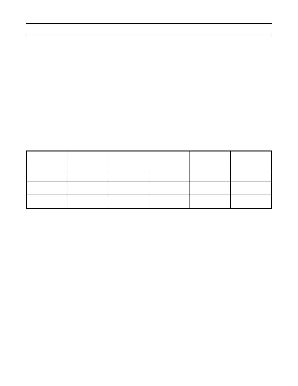
DEVICE INFORMATION
Device No. of pins On-chip RAM On-chip FLASH
LPC2119 64 16 kB 128 kB 2 LPC2129 64 16 kB 256 kB 2 -
LPC2292 144 16 kB 256 kB 2
LPC2294 144 16 kB 256 kB 4
Table 1: LPC2119/2129/2292/2294 device information
No. of CAN
channels
Note
with external
memory interface
with external
memory interface
Introduction 17 January 08, 2004
Page 18

Philips Semiconductors Preliminary User Manual
LPC2119/2129/2292/2294ARM-based Microc ontroller
ARCHITECTURAL OVERVIEW
The LPC2119/2129/2292/2294 consists of an ARM7TDMI-S CPU with emulation support, the ARM7 Local Bus for interface to
on-chip memory controllers, the AMBA Advanced High-performance Bus (AHB) for interface to the interrupt controller, and the
VLSI Peripheral Bus (VPB, a comp atible superset of ARM’ s AMBA Advanced Peripheral Bu s) for connection to on-c hip peripheral
functions. The LPC2119/2129/2292/2294 configures the ARM7TDMI-S processor in little-endian byte order.
AHB peripherals are allocated a 2 megabyte range of addresses at the very top of the 4 gigabyte ARM memory space. Each
AHB peripheral is allocated a 16 kilobyte address space within the AHB address space. LPC2119/2129/2292/2294 peripheral
functions (other than the interrupt controller) are connected to the VPB bus. The AHB to VPB bridge interfaces the VPB bus to
the AHB bus. VPB peripherals are also allocated a 2 megaby te range o f addresses , beginni ng at the 3 .5 gigabyte a ddress po int.
Each VPB peripheral is allocated a 16 kilobyte address space within the VPB address space.
The connection of on-chip pe ripherals to d evice pins i s controlled by a Pin Conne ction Block. This must be configured by software
to fit specific application requirements for the use of peripheral functions and pins.
ARM7TDMI-S PROCESSOR
The ARM7TDMI-S is a general purpose 32-bit microproce ssor, which offers high perfo rmance and very low pow er consumption .
The ARM architecture is based on Reduced Instruction Set Computer (RISC) principles, and the instruction set and related
decode mechanism are much simpler than those of microprogrammed Complex Instruction Set Computers. This simplicity
results in a high instruction throughput and impressive real-time interrupt response from a small and cost-effective processor
core.
Pipeline techniques are em plo ye d so tha t all parts of the processing and memory sy ste ms can operat e con tin uously. Typically,
while one instruction is being executed, its successor is being decoded, and a third instruction is being fetched from memory.
The ARM7TDMI-S processor also employs a unique architectural strategy known as THUMB, which makes it ideally suited to
high-volume applications with memory restrictions, or applications where code density is an issue.
The key idea behind THUMB is that of a super-reduced instruction set. Essentially, the ARM7TDMI-S processor has two
instruction sets:
• The standard 32-bit ARM instruction set.
• A 16-bit THUMB instruction set.
The THUMB set’s 16-bit ins truc tion length allows it to ap proa ch tw ic e th e de ns ity of s tan dard AR M c ode whil e retaining most of
the ARM’s performance advantage over a traditional 16-bit processor using 16-bit registers. This is possible because THUMB
code operates on the same 32-bit register set as ARM code.
THUMB code is able to provide up to 65% of the code size of ARM, and 160% of the performance of an equivalent ARM
processor connected to a 16-bit memory system.
The ARM7TDMI-S processor is described in detail in the ARM7TDMI-S Datasheet that can be found on official ARM website.
ON-CHIP FLASH MEMORY SYSTEM
The LPC2219 incorporate a 128 kB Flash memory system, while LPC2129/2292/2294 incorporate a 256 kB Flash memory
system. This mem ory ma y be u sed fo r both c ode an d data storage . Program ming of the Flash memo ry may be ac comp lishe d in
several ways: over the serial built-in JTAG interface, using In System Programming (ISP) and UART0, or by means of In
Application Programmi ng (IAP) capabilities. Th e application pro gram, using the In Appli cation Programmin g (IAP) functions, may
also erase and/or program the Flash while the application is running, allowing a great degree of flexibility for data storage field
firmware upgrades, etc.
Introduction 18 January 08, 2004
Page 19

Philips Semiconductors Preliminary User Manual
LPC2119/2129/2292/2294ARM-based Microc ontroller
ON-CHIP STATIC RAM
The LPC2119/2129/2 292/2294 provide a 1 6 k B s ta tic R AM m emory th at may be used for co de an d/o r da ta sto rage. The SRAM
supports 8-bit, 16-bit, and 32-bit accesses.
The SRAM controller incorpo r ate s a wri te-b ac k bu ffer i n ord er to p rev ent CPU s tal ls d urin g ba ck -to-back writes. The write-bac k
buffer always holds the last data sent by software to the SRAM. This data is only written to the SRAM when another write is
requested by software (the data is only written to the SRAM when software does another write). If a chip reset occurs, actual
SRAM contents will not reflect the most recent write request (i.e. after a "warm" chip reset, the SRAM does not reflect the last
write operation). Any software that checks SRAM contents after reset must take this into account. Two identical writes to a
location guarantee that the data will be present after a Reset. Alternatively, a dummy write operation before entering idle or
power-down mode will similarly guarantee that the last data written will be present in SRAM after a subsequent Reset.
Introduction 19 January 08, 2004
Page 20
Philips Semiconductors Preliminary User Manual
LPC2119/2129/2292/2294ARM-based Microc ontroller
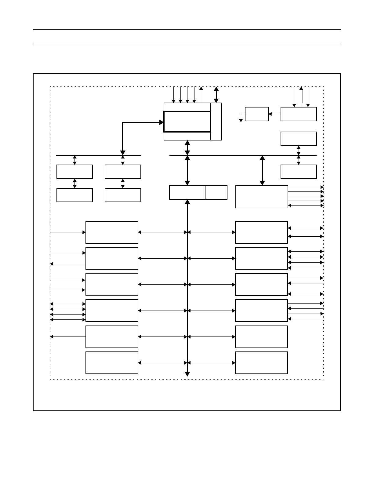
BLOCK DIAGRAM
Internal SRAM
Controller
16 kB
SRAM
EINT3:0
8 x CAP0
8 x MAT
Ain3:0
2
Ain7:4
P0.30:0
P1.31:16, 1:0
P2.31:0
P3.31:0
2
2
ARM7 Local Bus
External
Interrupts
Capture /
Compare
TIMER 0 & 1
Converter
2
General
Purpose I/O
Internal Flash
Controller
128/256 kB
FLASH
A/D
1
1
TMS
TRST
Test/Debug Interface
1
1
1
TDI
TCK
TDO
ARM7TDMI-S
AHB Bridge
AHB to VPB
Bridge
VPB (VLSI
Peripheral Bus)
PLL
System
Module
Emulation Trace
(Advanced High-performance Bus)
VPB
Divider
Clock
AMBA AHB
External Memory
Controller
I2C Serial
Interface
SPI Serial
Interfac es 0 & 1
UART 0 & 1
CAN
Xtal1
System
Functions
Vectored Interrupt
Controller
AHB
Decoder
2
DSR1,CTS1,D
Xtal2
RESET
CS3:0*
A23:0*
BLS3:0*
OE, WE*
D31:0*
SCL
SDA
SCK0,1
MOSI0,1
MISO0,1
SSEL0,1
TxD0,1
RxD0,1
CD1, RI1
TD2,1
RD2,1
2,3
TD4:3
2,3
RD4,3
PWM6:1
PWM0
Real Time
Clock
* Shared with GPIO
1
When Test/Debug Interface is used, GPIO/other functions sharing these pins are not available
2
LPC2292/2294 only.
3
LPC2294 only.
Watchdog
Timer
System
Control
Figure 1: LPC2119/2129/2292/2294 Block Diagram
Introduction 20 January 08, 2004
Page 21
Philips Semiconductors Preliminary User Manual
LPC2119/2129/2292/2294ARM-based Microc ontroller
LPC2119/2129/2292/2294 REGISTERS
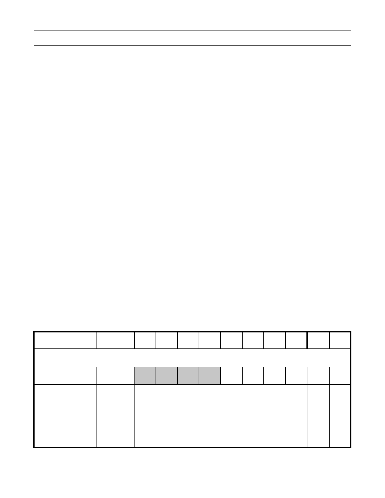
Accesses to registers in LPC21 19/2 12 9/22 92/2294 is restricted in the following ways :
1) user must NOT attempt to access any register locations not defined.
2) Access to any defined register locations must be str ictly for the functions for the registers.
3) Register bits labeled ’-’, ’0’ or ’1’ can ONLY be written and read as follows:
- ’-’ MUST be written with ’0’, but can return any value when read (even if it was written with ’0’). It is a reserved bit and may
be used in future derivatives.
- ’0’ MUST be written with ’0’, and will return a ’0’ when read.
- ’1’ MUST be written with ’1’, and will return a ’1’ when read.
The following table shows all registers available in LPC2119/2129/2292/2294 microcontroller sorted according to the address.
Access to the specific one can be categorized as either read/write, read only or write only (R/W, RO and WO respectively).
"Reset Value" field refe rs to the data stored in us ed/accessible bit s only. It does not inc lude reserved bits cont ent. Some registers
may contain undeterm ined data up on reset. In thi s case, reset value is ca tegorized as "un defined". Classificati on as "NA" is u sed
in case reset value is not applicable. Some registers in RTC are not affected by the chip reset. Their reset value is marked as *
and these registers must be initialized by software if the RTC is enabled.
Registers in LPC2119/2129/2292/2294 are 8, 16 or 32 bits wide. For 8 bit registers shown in Table 2, bit residing in the MSB
(The Most Significant Bi t) colu mn co rrespon ds to th e bit 7 o f that reg ister, wh ile bit in th e LSB (The Least Si gnific ant Bit) c olumn
corresponds to the bit 0 of the same register.
If a register is 1 6/3 2 bit wide, the b it res iding in t he top left corne r of i ts d escrip tion, is th e bit corre spond ing to the bit 1 5/31 o f the
register, while the bit in the bottom right corner corresponds to bit 0 of this register.
Examples: bit "EN A6" in PWM P CR reg ist er ( add res s 0 xE0 014 04 C) rep res ents t he bit at pos iti on 14 in this register; bits 1 5, 8, 7
and 0 in the same register are reserved. Bit "Stop on MR6" in PWMMCR register (0xE001 4014) corresponds to the bit at positi on
20; bits 31 to 21 of the same register are reserved.
Unused (reserved) bits are marked with "-" and represented as gray fields. Access to them is restricted as already described.
Table 2: LPC2119/2129/2292/2294 Registers
Address
Offset
WD
0xE0000000
0xE0000004 WDTC
Name Description MSB LSB Access
WD
MOD
Watchdog
mode register
Watchdog
timer
constant
register
- - - -
WD
INTWDTOF
32 bit data R/W 0xFF
WDRE
SET
WDEN R/W 0
Reset
Value
Watchdog
WD
0xE0000008
FEED
feed
sequence
register
8 bit data (0xAA fallowed by 0x55) WO NA
Introduction 21 January 08, 2004
Page 22
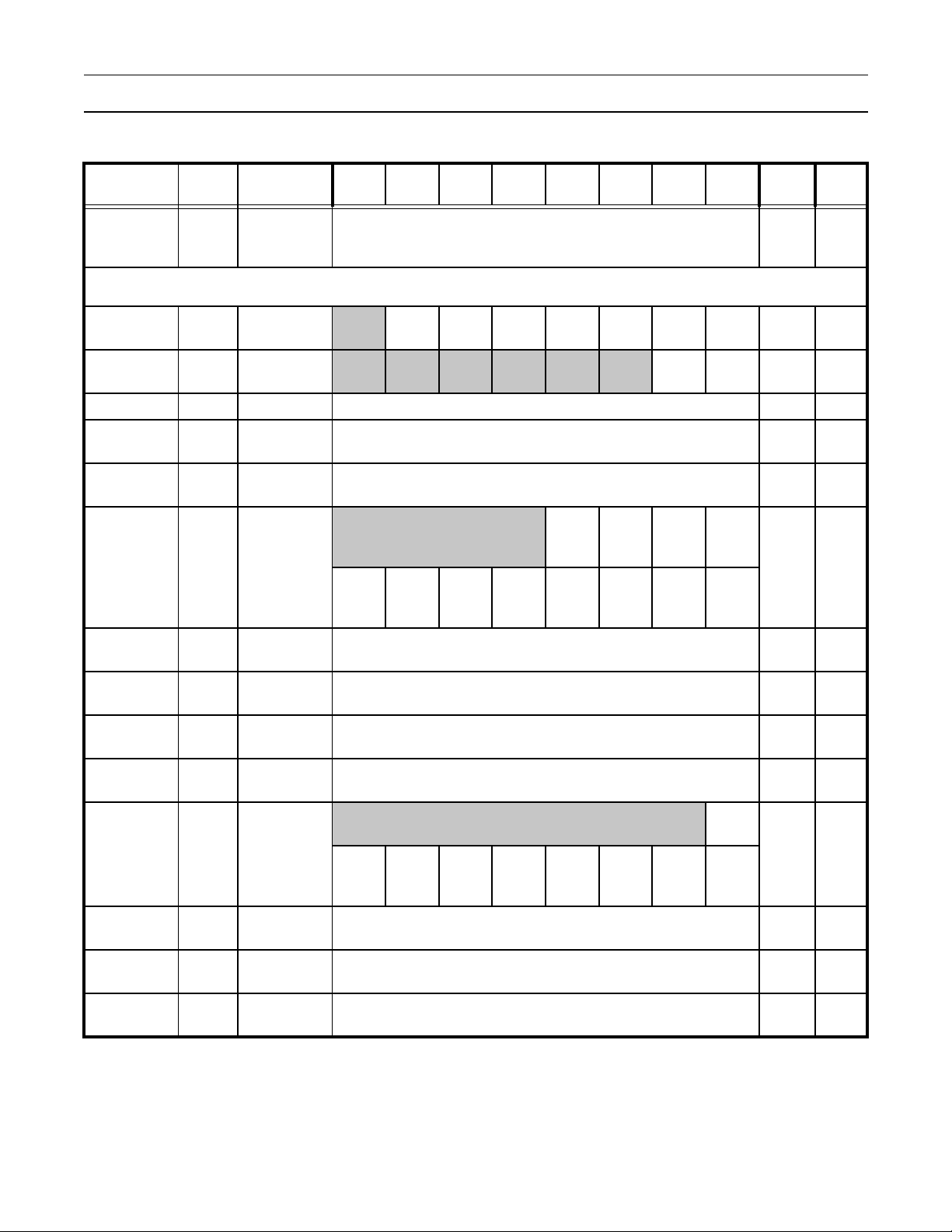
Philips Semiconductors Preliminary User Manual
LPC2119/2129/2292/2294ARM-based Microc ontroller
Table 2: LPC2119/2129/2292/2294 Registers
Address
Offset
0xE000000C WDTV
TIMER0
0xE0004000 T0IR
0xE0004004 T0TCR
0xE0004008 T0TC T0 Counter 32 bit data RW 0
0xE000400C T0PR
0xE0004010 T0PC
0xE0004014 T0MCR
Name Description MSB LSB Access
Watchdog
timer value
register
T0 Interrupt
Register
T0 Control
Register
T0 Prescale
Register
T0 Prescale
Counter
T0 Match
Control
Register
CR2
Int.
- - - - - -
4 reserved (-) bits
Reset
MR2
on
Int. on
MR2
CR1
Int.
Stop
on
MR1
32 bit data RO 0xFF
CR0
Int.
Reset
on
MR1
MR3
Int.
32 bit data R/W 0
32 bit data R/W 0
Stop
on
MR3
Int. on
MR1
MR2
Int.
Reset
on
MR3
Stop
on
MR0
MR1
Int.
CTR
Enable
Int. on
MR3
Reset
on
MR0
MR0
Int.
CTR
Reset
Stop
on
MR2
Int. on
MR0
R/W 0
R/W 0
R/W 0
Reset
Value
0xE0004018 T0MR0
0xE000401C T0MR1
0xE0004020 T0MR2
0xE0004024 T0MR3
0xE0004028 T0CCR
0xE000402C T0CR0
0xE0004030 T0CR1
0xE0004034 T0CR2
T0 Match
Register 0
T0 Match
Register 1
T0 Match
Register 2
T0 Match
Register 3
T0 Capture
Control
Register
T0 Capture
Register 0
T0 Capture
Register 1
T0 Capture
Register 2
Int. on
Cpt.2
falling
Int. on
Cpt.2
rising
32 bit data R/W 0
32 bit data R/W 0
32 bit data R/W 0
32 bit data R/W 0
7 reserved (-) bits
Int. on
Cpt.1
Int. on
Cpt.1
falling
32 bit data RO 0
32 bit data RO 0
32 bit data RO 0
Int. on
Cpt.1
rising
Int. on
Cpt.0
Int. on
Cpt.0
falling
Int. on
Cpt.2
Int. on
Cpt.0
rising
R/W 0
Introduction 22 January 08, 2004
Page 23
Philips Semiconductors Preliminary User Manual
LPC2119/2129/2292/2294ARM-based Microc ontroller
Table 2: LPC2119/2129/2292/2294 Registers
Address
Offset
0xE000403C T0EMR
TIMER1
0xE0008000 T1IR
0xE0008004 T1TCR
0xE0008008 T1TC T1 Counter 32 bit data RW 0
0xE000800C T1PR
0xE0008010 T1PC
0xE0008014 T1MCR
Name Description MSB LSB Access
Ext.
Int.
on
on
External Match
Control 2
Ext.
Mtch.1
MR1
Int.
CTR
Enable
Int. on
MR3
Reset
on
MR0
Ext.
Mtch.0
MR0
Int.
CTR
Reset
Stop
on
MR2
Int. on
MR0
R/W 0
R/W 0
R/W 0
R/W 0
T0 External
Match
Register
T1 Interrupt
Register
T1 Control
Register
T1 Prescale
Register
T1 Prescale
Counter
T1 Match
Control
Register
6 reserved (-) bits
External Match
Control 1
CR3
Int.
Reset
on
MR2
CR2
- - - - - -
4 reserved (-) bits
Int. on
MR2
Int.
External Match
Control 0
CR1
Int.
Stop
on
MR1
CR0
Int.
32 bit data R/W 0
32 bit data R/W 0
Reset
on
MR1
-
MR3
Int.
Stop
on
MR3
Int. on
MR1
Mtch2.
MR2
Reset
MR3
Stop
MR0
Reset
Value
0xE0008018 T1MR0
0xE000801C T1MR1
0xE0008020 T1MR2
0xE0008024 T1MR3
0xE0008028 T1CCR
0xE000802C T1CR0
0xE0008030 T1CR1
0xE0008034 T1CR2
T1 Match
Register 0
T1 Match
Register 1
T1 Match
Register 2
T1 Match
Register 3
T1 Capture
Control
Register
T1 Capture
Register 0
T1 Capture
Register 1
T1 Capture
Register 2
4 reserved (-) bits
Int. on
Cpt.2
falling
Int. on
Cpt.2
rising
Int. on
Cpt.1
32 bit data R/W 0
32 bit data R/W 0
32 bit data R/W 0
32 bit data R/W 0
Int. on
Cpt.3
Int. on
Cpt.1
falling
Int. on
Cpt.1
rising
32 bit data RO 0
32 bit data RO 0
32 bit data RO 0
Int. on
Cpt.3
falling
Int. on
Cpt.0
Int. on
Cpt.3
rising
Int. on
Cpt.0
falling
Int. on
Cpt.2
R/W 0
Int. on
Cpt.0
rising
Introduction 23 January 08, 2004
Page 24
Philips Semiconductors Preliminary User Manual
LPC2119/2129/2292/2294ARM-based Microc ontroller
Table 2: LPC2119/2129/2292/2294 Registers
Address
Offset
Name Description MSB LSB Access
0xE0008038 T1CR3
0xE000803C T1EMR
UART0
U0RBR
(DLAB=0)
0xE000C000
U0THR
(DLAB=0)
U0DLL
(DLAB=1)
U0IER
0xE000C004
(DLAB=0)
T1 Capture
Register 3
T1 External
Match
Register
U0 Receiver
Buffer
Register
U0 Transmit
Holding
Register
U0 Divisor
Latch LSB
U0 Interrupt
Enable
Register
32 bit data RO 0
4 reserved (-) bits
External Match
Control 1
External Match
Control 0
External Match
Control 3
Ext.
Mtch.3
8 bit data RO
8 bit data WO N A
8 bit data R/W 0x01
00000
Ext.
Mtch2.
En. Rx
Line
Status
Int.
External Match
Control 2
Ext.
Mtch.1
Enable
THRE
Int.
Ext.
Mtch.0
En. Rx
Data
Av.Int.
Reset
Value
R/W 0
un-
defined
R/W 0
U0DLM
(DLAB=1)
U0IIR
0xE000C008
U0FCR
0xE000C00C U0LCR
0xE000C014 U0LSR
0xE000C01C U0SCR
UART1
U0 Divisor
Latch MSB
U0 Interrupt
ID Register
U0 FIFO
Control
Register
U0 Line
Control
Register
U0 Line
Status
Register
U0 Scratch
Pad Register
8 bit data R/W 0
FIFOs Enabled 0 0 IIR3 IIR2 IIR1 IIR0 R O 0x01
Rx Trigger
DLAB
Set
Break
- - -
Stick
Parity
Even
Parity
Select
Parity
Enable
U0 Tx
FIFO
Reset
Nm. of
Stop
Bits
U0 Rx
FIFO
Reset
U0
FIFO
Enable
Word Length
Select
WO 0
R/W 0
Rx
FIFO
TEMT THRE BI FE PE OE DR RO 0x60
Error
8 bit data R/W 0
Introduction 24 January 08, 2004
Page 25
Philips Semiconductors Preliminary User Manual
LPC2119/2129/2292/2294ARM-based Microc ontroller
Table 2: LPC2119/2129/2292/2294 Registers
Address
Offset
Name Description MSB LSB Access
U1RBR
(DLAB=0)
0xE0010000
U1THR
(DLAB=0)
U1DLL
(DLAB=1)
U1IER
0xE0010004
(DLAB=0)
U1DLM
(DLAB=1)
U1IIR
0xE0010008
U1FCR
0xE001000C U1LCR
0xE0010010
U1
MCR
0xE0010014 U1LSR
U1 Receiver
Buffer
Register
U1 Transmit
Holding
Register
U1 Divisor
Latch LSB
U1 Interrupt
Enable
Register
U1 Divisor
Latch MSB
U1 Interrupt
ID Register
U1 FIFO
Control
Register
U1 Line
Control
Register
U1 Modem
Control
Register
U1 Line
Status
Register
Reset
Value
8 bit data RO
un-
defined
8 bit data WO N A
8 bit data R/W 0x01
En.
0000
Mdem
Satus
En. Rx
Status
Int.
Line
Int.
Enable
THRE
Int.
En. Rx
Data
Av.Int.
R/W 0
8 bit data R/W 0
FIFOs Enabled 0 0 IIR3 IIR2 IIR1 IIR0 RO 0x01
Rx Trigger
DLAB
Set
Break
- - -
Stick
Parity
000
Even
Parity
Select
Loop
Back
U0 Tx
FIFO
Reset
Parity
Enable
Nm. of
Stop
0 0 RTS DTR R/W 0
Bits
U0 Rx
FIFO
Reset
U0
FIFO
Enable
Word Length
Select
WO 0
R/W 0
Rx
FIFO
TEMT THRE BI FE PE OE DR RO 0x60
Error
U1
U1 Scratch
Pad Register
U1 Modem
Status
Register
8 bit data R/W 0
DCD RI DSR CTS
Delta
DCD
Trailing
Edge
RI
Delta
DSR
Delta
CTS
RO 0
0xE001001C U1SCR
0xE0010018
MSR
PWM
0xE0014000
0xE0014004
0xE0014008
IR
PWM
Interrupt
Register
PWM Timer
Control
Register
PWM
PWM
TCR
PWMTCPWM Timer
Counter
- - - - -
- - - -
- - - -
MR3
PWM
Enable
32 bit data RW 0
Int.
MR6
Int.
MR2
Int.
MR5
Int.
MR4
Int.
R/W 0
MR1
Int.
CTR
Reset
MR0
Int.
CTR
Enable
R/W 0
Introduction 25 January 08, 2004
Page 26
Philips Semiconductors Preliminary User Manual
LPC2119/2129/2292/2294ARM-based Microc ontroller
Table 2: LPC2119/2129/2292/2294 Registers
Address
Offset
0xE001400C
0xE0014010
0xE0014014
0xE0014018
0xE001401C
0xE0014020
Name Description MSB LSB Access
PR
PC
PWM
Prescale
Register
PWM
Prescale
Counter
PWM Match
Control
Register
PWM Match
Register 0
PWM Match
Register 1
PWM Match
Register 2
11 reserved (-) bits
Int. on
MR5
Reset
on
MR2
Stop
on
MR4
Int. on
MR2
Reset
on
MR4
Stop
on
MR1
32 bit data R/W 0
32 bit data R/W 0
Stop
MR6
Int. on
MR4
Reset
MR1
on
on
Reset
on
MR6
Stop
on
MR3
Int. on
MR1
Int. on
MR6
Reset
on
MR3
Stop
on
MR0
Stop
on
MR5
Int. on
MR3
Reset
on
MR0
Reset
on
MR5
Stop
on
MR2
Int. on
MR0
R/W 0
32 bit data R/W 0
32 bit data R/W 0
32 bit data R/W 0
PWM
PWM
PWM
MCR
PWM
MR0
PWM
MR1
PWM
MR2
Reset
Value
0xE0014024
0xE0014040
0xE0014044
0xE0014048
0xE001404C
0xE0014050
2
C
I
0xE001C000
PWM
MR3
PWM
MR4
PWM
MR5
PWM
MR6
PWM
PCR
PWM
LER
I2CON
SET
0xE001C004 I2STAT
0xE001C008 I2DAT
PWM Match
Register 3
PWM Match
Register 4
PWM Match
Register 5
PWM Match
Register 6
PWM Control
Register
PWM Latch
Enable
Register
2
C Control
I
Set Register
2
C Status
I
Register
2
C Data
I
Register
32 bit data R/W 0
32 bit data R/W 0
32 bit data R/W 0
32 bit data R/W 0
- ENA6 ENA5 ENA4 ENA3 ENA2 ENA1 R/W 0
- SEL6 SEL5 SEL4 SEL3 SEL2 SEL1 -
Ena.
PWM
-
M6
Latch
Ena.
PWM
M5
Latch
Ena.
PWM
M4
Latch
Ena.
PWM
M3
Latch
Ena.
PWM
M2
Latch
Ena.
PWM
M1
Latch
Ena.
PWM
M0
Latch
R/W 0
-I2ENSTASTOSIAA - -R/W0
5 bit Status 0 0 0 RO 0xF8
8 bit data R/W 0
Introduction 26 January 08, 2004
Page 27
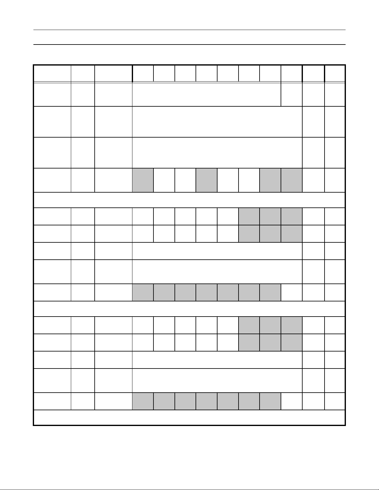
Philips Semiconductors Preliminary User Manual
LPC2119/2129/2292/2294ARM-based Microc ontroller
Table 2: LPC2119/2129/2292/2294 Registers
Address
Offset
0xE001C00C
0xE001C010
0xE001C014
0xE001C018
SPI0
0xE0020000
0xE0020004
0xE0020008
0xE002000C
0xE002001C
Name Description MSB LSB Access
2
C Slave
I
I2
ADR
Address
Register
7 bit data GC R/W 0
SCL Duty
I2
SCLH
Cycle
Register High
16 bit data R/W 0x04
Half Word
SCL Duty
I2
SCLL
Cycle
Register Low
16 bit data R/W 0x04
Half Word
2
C Control
S0
S0
S0
S0
S0
I
Clear
Register
SPI0 Control
Register
SPI0 Status
Register
SPI0 Data
Register
SPI0 Clock
Counter
Register
SPI0
Interrupt Flag
- I2ENC STAC - SIC AAC - -WONA
SPIE LSBF MSTR CPOL CPHA
SPIF WCOL ROVR MODF ABRT
- - -R/W0
- - -RO0
8 bit data R/W 0
8 bit data R/W 0
- - - - - - -
SPI
Int.
R/W 0
I2CON
CLR
SPCR
SPSR
SPDR
SPCCR
SPINT
Reset
Value
SPI1
0xE0030000
0xE0030004
0xE0030008
0xE003000C
0xE003001C
SPCR
S1
SPSR
S1
SPDR
S1
SPCCR
S1
SPINT
SPI1 Control
Register
SPI1 Status
Register
SPI1 Data
Register
SPI1 Clock
Counter
Register
SPI1
Interrupt Flag
SPIE LSBF MSTR CPOL CPHA
SPIF WCOL ROVR MODF ABRT
8 bit data R/W 0
8 bit data R/W 0
- - - - - - -
- - -R/W0
- - -RO0
SPI
Int.
R/W 0
S1
RTC
Introduction 27 January 08, 2004
Page 28
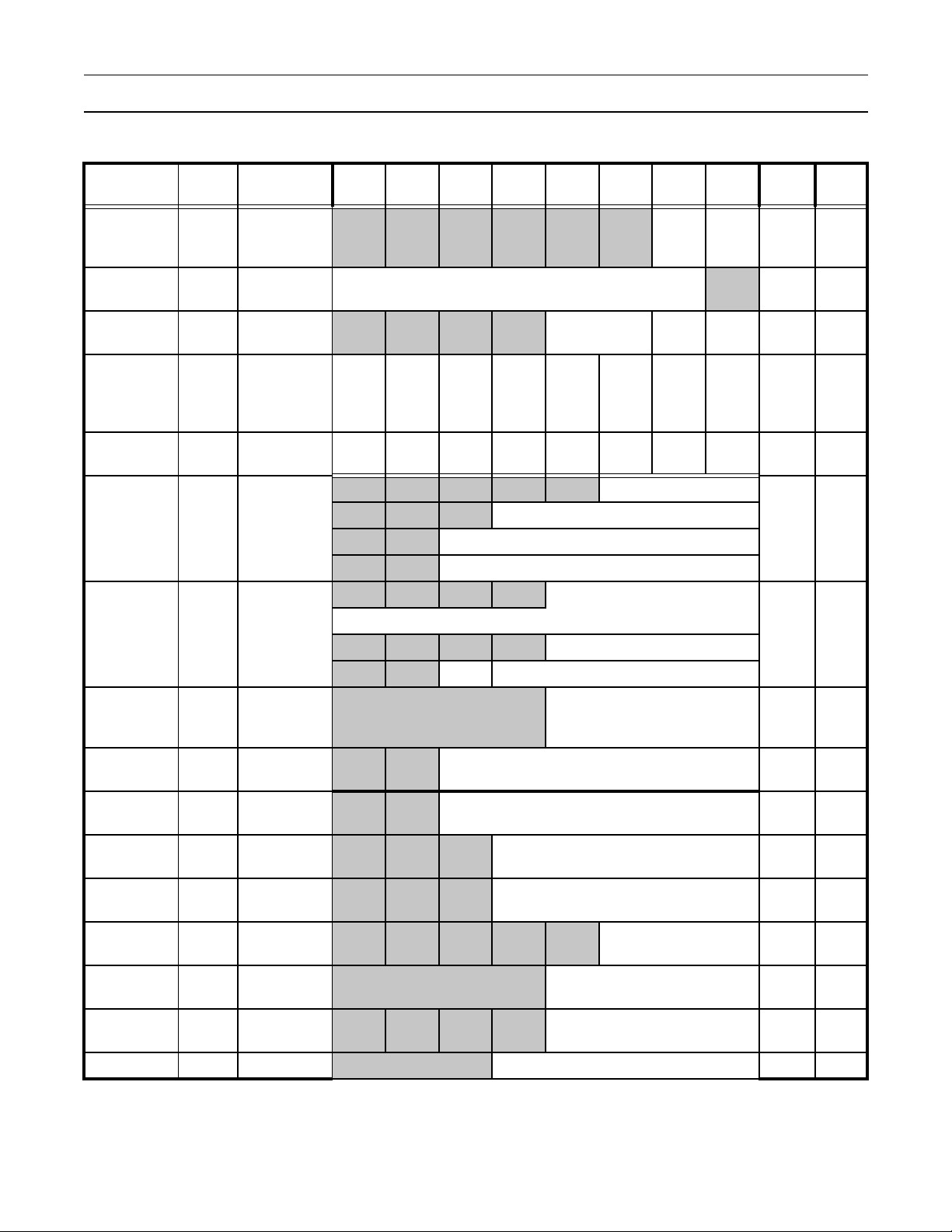
Philips Semiconductors Preliminary User Manual
LPC2119/2129/2292/2294ARM-based Microc ontroller
Table 2: LPC2119/2129/2292/2294 Registers
Address
Offset
Name Description MSB LSB Access
0xE0024000 ILR
0xE0024004 CTC
0xE0024008 CCR
0xE002400C CIIR
0xE0024010 AMR
0xE0024014
0xE0024018
CTIME0
CTIME1
Interrupt
Location
Register
Clock Tick
Counter
Clock Control
Register
Counter
Increment
Interrupt
Register
Alarm Mask
Register
Consolidated
Time
Register 0
Consolidated
Time
Register 1
- - - - - -
15 bit data
- - - - CTTEST
RTC
ALF
CTC
RST
RTC
CIF
-RO*
CLK
EN
IM
YEARIMMONIMDOYIMDOWIMDOMIMHOURIMMINIMSEC
AMR
YEAR
AMR
MON
AMR
DOY
AMR
DOW
AMR
DOM
AMR
HOUR
AMR
MIN
AMR
SEC
- - - - - 3 bit Day of Week
- - - 5 bit Hours
- - 6 bit Minutes
- - 6 bit Seconds
- - - 12 bit Year
- - - - 4 bit Month
- - - 5 bit Day of Month
Reset
Value
R/W *
R/W *
R/W *
R/W *
RO *
RO *
Consolidated
0xE002401C
CTIME2
Time
Register 2
0xE0024020 SEC
0xE0024024 MIN
0xE0024028 HOUR
0xE002402C DOM
0xE0024030 DOW
0xE0024034 DOY
0xE0024038
MONTH
Seconds
Register
Minutes
Register
Hours
Register
Day of Month
Register
Day of Week
Register
Day of Year
Register
Months
Register
0xE002403C YEAR Year Register
reserved (-) 20 bits 12 bit Day of Year RO *
- - 6 bit data R/W *
- - 6 bit data R/W *
- - - 5 bit data R/W *
- - - 5 bit data R/W *
- - - - - 3 bit data R/W *
reserved (-) 7 bits 9 bit data R/W *
- - - - 4 bit data R/W *
reserved (-) 4 bits 12 bit data R/W *
Introduction 28 January 08, 2004
Page 29
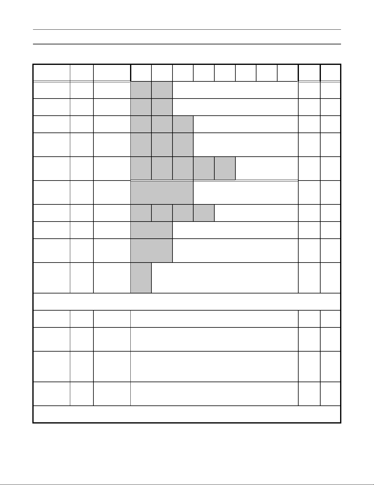
Philips Semiconductors Preliminary User Manual
LPC2119/2129/2292/2294ARM-based Microc ontroller
Table 2: LPC2119/2129/2292/2294 Registers
Address
Offset
0xE0024060
0xE0024064
0xE0024068
0xE002406C
0xE0024070
0xE0024074
0xE0024078
0xE002407C
0xE0024080
0xE0024084
Name Description MSB LSB Access
AL
SEC
AL
MIN
AL
HOUR
AL
DOM
AL
DOW
AL
DOY
AL
MON
AL
YEAR
PRE
INT
PRE
FRAC
Alarm value
for Seconds
Alarm value
for Minutes
Alarm value
for Hours
Alarm value
for Day of
Month
Alarm value
for Day of
Week
Alarm value
for Day of
Year
Alarm value
for Months
Alarm value
for Year
Prescale
value, integer
portion
Prescale
value,
fractional
portion
- - 6 bit data R/W *
- - 6 bit data R/W *
- - - 5 bit data R/W *
- - - 5 bit data R/W *
- - - - - 3 bit data R/W *
reserved (-) 7 bits 9 bit data R/W *
- - - - 4 bit data R/W *
reserved
(-) 4 bits
reserved
(-) 3 bits
- 15 bit data R/W 0
12 bit data R/W *
13 bit data R/W 0
Reset
Value
GPIO
0xE0028000 IOPIN
0xE0028004 IOSET
0xE0028008 IODIR
0xE002800C IOCLR
Pin Connet Block
GPIO Pin
value regi ster
GPIO 0
Output set
register
GPIO 0
Direction
control
register
GPIO 0
Output clear
register
32 bit data RO NA
32 bit data R/W 0
32 bit data R/W 0
32 bit data WO 0
Introduction 29 January 08, 2004
Page 30
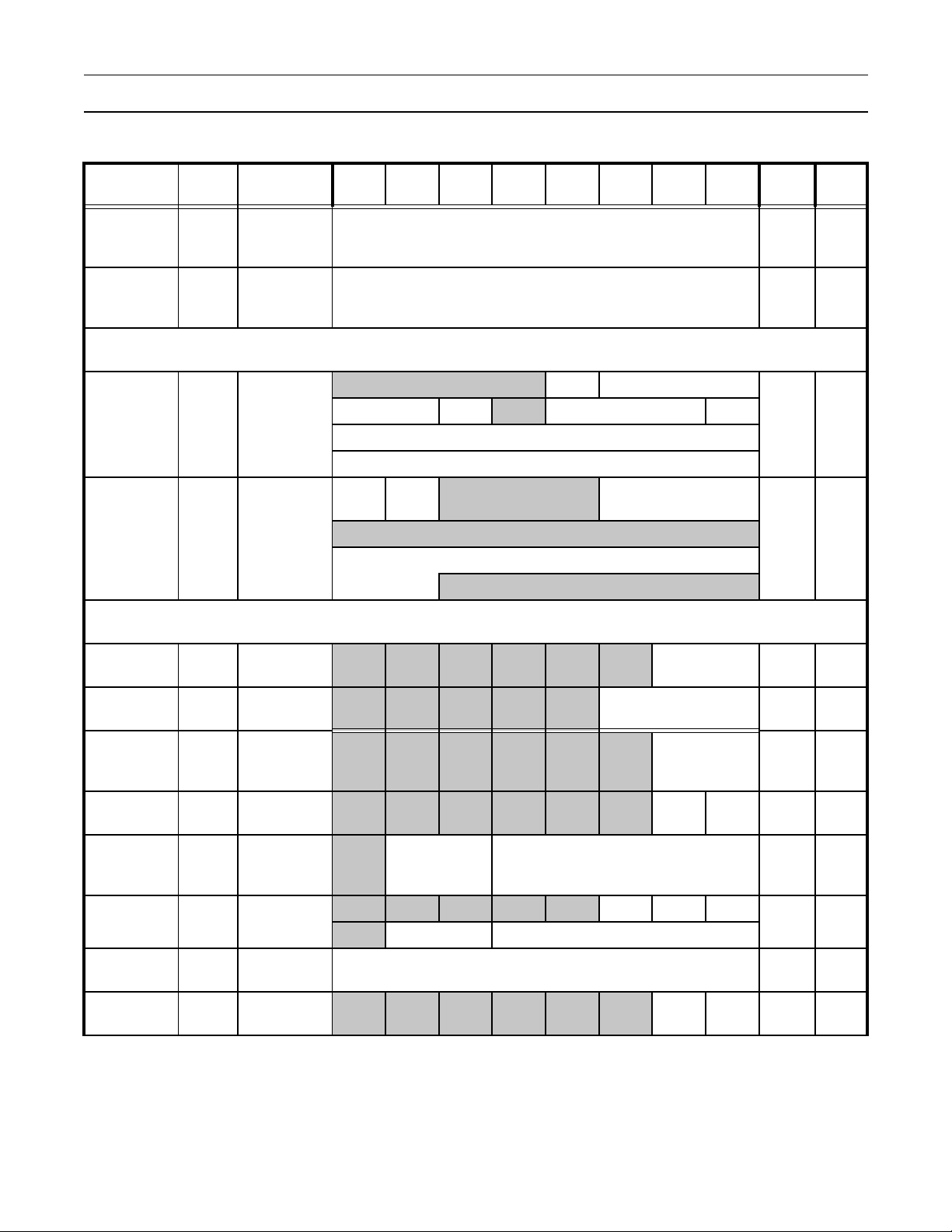
Philips Semiconductors Preliminary User Manual
LPC2119/2129/2292/2294ARM-based Microc ontroller
Table 2: LPC2119/2129/2292/2294 Registers
Address
Offset
0xE002C000
0xE002C004
Name Description MSB LSB Access
Pin funct i on
PIN
PIN
select
register 0
Pin funct i on
select
register 1
SEL0
SEL1
ADC
0xE0034000 ADCR ADC Control
register
0xE0034004 ADDR ADC Data
register
TEST1:0 PDN
DONE
OVER
RUN
32 bit data R/W 0
32 bit data R/W 0
- EDGE START
-CLKS
8 bit data
8 bit data
- CHN
10 bit data
-
Reset
Value
BURST
RW 01
RW x
System Control Block
0xE01FC000
0xE01FC004
0xE01FC040
0xE01FC080
0xE01FC084
0xE01FC088
0xE01FC08C
MAMCRMAM control
MAM
TIM
MEM
MAP
PLL
CON
PLL
CFG
PLL
STAT
PLL
FEED
0xE01FC0C0 PCON
register
MAM timing
control
Memory
mapping
control
PLL control
register
PLL
configuration
register
PLL status
register
PLL feed
register
Power control
register
- - - - - - 2 bit data R/W 0
- - - - - 3 bit data R/W 0x07
- - - - - - 2 bit data R/W 0
- - - - - - PLLC PLLE R/W 0
- 2bit data PSEL 5 bit data MSEL R/W 0
- - - - -
PLOCK
PLLC PLLE
RO 0
- 2bit data PSEL 5 bit data MSEL
8 bit data WO N A
- - - - - - PD IDL R/W 0
Introduction 30 January 08, 2004
Page 31
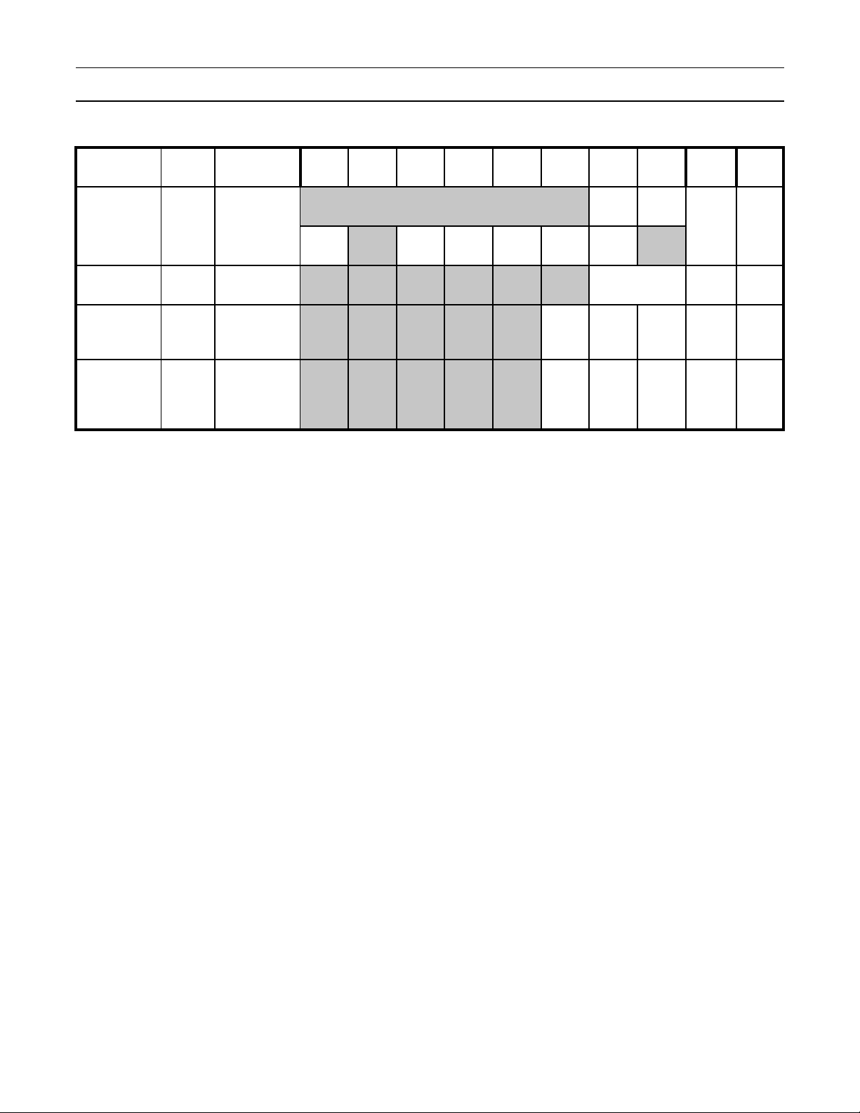
Philips Semiconductors Preliminary User Manual
LPC2119/2129/2292/2294ARM-based Microc ontroller
Table 2: LPC2119/2129/2292/2294 Registers
Address
Offset
0xE01FC0C4 PCONP
0xE01FC100
0xE01FC140
0xE01FC144
Name Description MSB LSB Access
VPB
DIV
EXT
INT
EXT
WAKE
Power control
for
peripherals
VPB divider
control
External
interrupt flag
register
External
interrupt
wakeup
register
reserved (-) 22 bits
PC
I2C
- - - - - - 2 bit data R/W 0
- - - - - EINT2 EINT1 EINT0 R/W 0
- - - - -
PC
PWM0PCURT1PCURT0PCTIM1PCTIM0
EXT
WAKE
2
PC
RTCPCSPI
EXT
WAKE
WAKE0R/W 0
1
R/W 0x3BE
-
EXT
Reset
Value
Introduction 31 January 08, 2004
Page 32

Philips Semiconductors Preliminary User Manual
LPC2119/2129/2292/2294ARM-based Microc ontroller
2. LPC2119/2129/2292/2294 MEMORY ADDRESSING
MEMORY MAPS
The LPC2119/2129/ 2292/2294 incor porates se veral dist inct memory regions, shown i n the follo wing fig ures. Figur e 2 shows th e
overall map of the entire address space from the user program viewpoint following reset. The interrupt vector area supports
address re-mapping, which is described later in this section.
4.0 GB
3.75 GB
3.5 GB
3.0 GB
2.0 GB
AHB Peripherals
VPB Peripherals
Reserved for
External Memory
Boot Block
(re-mapped from On-Chip Flash memory)
Reserved for
On-Chip Memory
0xFFFF FFFF
0xF000 0000
0xE000 0000
0xC000 0000
0x8000 0000
0x4000 1FFF
0x4000 0000
0x0004 0000
0x0003 FFFF
0x0002 0000
0x0001 FFFF
0x0000 0000
1.0 GB
0.0 GB
16 kB On-Chip Static RAM
256 kB On-Chip Non-Volatile Memory
(LPC2129/2292/2294)
128 kB On-Chip Non-Volatile Memory
(LPC2119)
Figure 2: System Memory Map
LPC2119/2129/2292/2294 Memory Addressing 32 January 08, 2004
Page 33

Philips Semiconductors Preliminary User Manual
LPC2119/2129/2292/2294ARM-based Microc ontroller
Notes:
- AHB section is
128 x 16 kB blocks
(totaling 2 MB).
- VPB section is
128 x 16 kB blocks
(totaling 2 MB).
4.0 GB
4.0 GB - 2 MB
3.75 GB
AHB Peripherals
0xFFFF FFFF
0xFFE0 0000
0xFFDF FFFF
Reserved
0xF000 0000
0xEFFF FFFF
Reserved
3.5 GB + 2 MB
VPB Peripherals
3.5 GB
Figure 3: Peripheral Memory Map
Figures 3 through 5 show different views of the peripheral address space. Both the AHB and VPB peripheral areas are 2
megabyte spaces whic h are divided up into 128 periph erals. Each peripheral space is 16 kilobytes in size . This allows simplify ing
the address decod ing for ea ch perip heral. All periphera l registe r addresses are wor d aligned (to 32-bi t boundar ies) regard less of
their size. This eliminates the need for byte lane mappi ng h ardw a re tha t woul d be required to allow byte (8-bit) o r hal f-w ord (16bit) accesses to occur at smaller boundaries. An implication of this is that word and half-word registers must be accessed all at
once. For example, it is not possible to read or write the upper byte of a word register separately.
0xE020 0000
0xE01F FFFF
0xE000 0000
LPC2119/2129/2292/2294 Memory Addressing 33 January 08, 2004
Page 34
Philips Semiconductors Preliminary User Manual
LPC2119/2129/2292/2294ARM-based Microc ontroller
Vectored Interrupt Controller
(AHB peripheral #126)
(AHB peripheral #125)
(AHB peripheral #124)
(AHB peripheral #3)
(AHB peripheral #2)
0xFFFF F000 (4G - 4K)
0xFFFF C000
0xFFFF 8000
0xFFFF 4000
0xFFFF 0000
0xFFE1 000 0
0xFFE0 C000
(AHB peripheral #1)
(AHB peripheral #0)
Figure 4: AHB Peripheral Map
0xFFE0 800 0
0xFFE0 400 0
0xFFE0 000 0
LPC2119/2129/2292/2294 Memory Addressing 34 January 08, 2004
Page 35
Philips Semiconductors Preliminary User Manual
LPC2119/2129/2292/2294ARM-based Microc ontroller
System Control Block
(VPB peripheral #127)
(VPB peripherals #14-126)
not used
10 bit A/D
(VPB peripheral #13)
SPI1
(VPB peripheral #12)
Pin Connect Block
(VPB peripheral #11)
GPIO
(VPB peripheral #10)
RTC
(VPB peripheral #9)
SPI0
(VPB peripheral #8)
2
C
I
(VPB peripheral #7)
not used
(VPB peripheral #6)
PWM0
(VPB peripheral #5)
UART1
(VPB peripheral #4)
UART0
(VPB peripheral #3)
TIMER1
(VPB peripheral #2)
TIMER0
(VPB peripheral #1)
Watchdog Timer
(VPB peripheral #0)
0xE01F FFFF
0xE01F C000
0xE003 8000
0xE003 4000
0xE003 0000
0xE002 C000
0xE002 8000
0xE002 4000
0xE002 0000
0xE001 C000
0xE001 8000
0xE001 4000
0xE001 0000
0xE000 C000
0xE000 8000
0xE000 4000
0xE000 0000
Figure 5: VPB Peripheral Map
LPC2119/2129/2292/2294 Memory Addressing 35 January 08, 2004
Page 36

Philips Semiconductors Preliminary User Manual
LPC2119/2129/2292/2294ARM-based Microc ontroller
LPC2119/2129/2292/2294 MEMORY RE-MAPPING AND BOOT BLOCK
Memory Map Concepts and Operating Modes
The basic concept on the LPC2119 /2129/229 2/2294 is that eac h memory are a has a "nat ural" loca tion in the me mory map. Thi s
is the address range for which code residing in that area is written. The bulk of each memory space remains permanently fixed
in the same location, eliminating the need to have portions of the code designed to run in different address ranges.
Because of the location of the interrupt vectors on the ARM7 processor (at addresses 0x0000 0000 through 0x0000 001C, as
shown in Table 3 below), a sma ll portion of the Boot Block and SRAM spa ces need to be re-ma pped in order to al low alternati ve
uses of interrupts in the different operating modes described in Table 4. Re-mapping of the interrupts is accomplished via the
Memory Mapping Control feature described in the System Control Block section.
Table 3: ARM Exception Vector Locations
Address Exception
0x0000 0000 Reset
0x0000 0004 Undefined Instruction
0x0000 0008 Software Interrupt
0x0000 000C Prefetch Abort (instruction fetch memory fault)
0x0000 0010 Data Abort (data access memory fault)
0x0000 0014 Reserved *
0x0000 0018 IRQ
0x0000 001C FIQ
*: Identified as reserved in ARM do cumen tat ion, this locatio n is used by the Boot Loade r as the Valid Use r Program ke y. This is
descibed in detail in Flash Memory System and Programming on page 228.
Table 4: LPC2119/2129/2292/2294 Memory Mapping Modes
Mode Activation Usage
Boot Loader
mode
User Flash
mode
User RAM
mode
User External
mode
Hardware activation
by any Reset
Software activation
by Boot code
Software activation
by User program
Activated by
BOOT1:0 pins not
11 at Reset
The Boot Loader always
mapped to the bottom of memory to allow handling exceptions and using interrupts
during the Boot Loading process.
Activated by Boot Loader w hen a valid User Progra m Signature is recogni zed in memory
and Boot Loader operation is not forced. Interrupt vectors are not re-mapped and are
found in the bottom of the Flash memory.
Activated by a User Program as de sir ed. In terru pt vectors are re-mapped to the bottom
of the Static RAM.
Activated by the Boot Loader when either or both BOOT pins are low at the end of
RESET low. Interrupt vectors are re-mapped from the bottom of the external memory
map.
Note: This mode is available in LPC2292/2294 only!
executes after any reset. The Boot Block interrupt vectors are
LPC2119/2129/2292/2294 Memory Addressing 36 January 08, 2004
Page 37

Philips Semiconductors Preliminary User Manual
LPC2119/2129/2292/2294ARM-based Microc ontroller
Memory Re-Mapping
In order to allo w for com patibili ty with future der ivativ es, the en tire Boot Block i s mapped to the top o f the on -chip mem ory space.
In this manner, the use of larger or smaller flash modules will not require changing the location of the Boot Block (which would
require changing the Boot Loader code itself ) or changing the mappin g of the Boot Block interru pt vectors. Memo ry spaces other
than the interrupt vectors remain in fixed locations. Figure 6 shows the on-chip memory mapping in the modes defined above.
The portion of memory that is re-mapped to allow interrupt processing in different modes includes the interrupt vector area (32
bytes) and an addition al 32 bytes, for a total of 64 bytes. The re-mapped code locations ove rlay addresses 0x0000 0000 throu gh
0x0000 003F. A typical u ser progra m in th e Flash memory c an plac e the e ntire FIQ handler at addre ss 0x0000 001C without a ny
need to consider memory boundaries. The vector contained in the SRAM, external memory, and Boot Block must contain
branches to the actual interrupt handlers, or to other instructions that accomplish the branch to the interrupt handlers.
There are three reasons this configuration was chosen:
1. To give the FIQ handler in the Flash memory the advantage of not having to take a memory boundary caused by the remapping into account.
2. Minimize the need to for th e SR AM and Boot Block vectors to deal wi th a rbitrary boundaries in the middl e of code space.
3. To provide space to store constants for jumping beyond the range of single word branch instructions.
Re-mapped memory are as, includin g the Boot Block and interr upt vectors, con tinue to appear in their original loc ation in addition
to the re-mapped address.
Details on re-mapping and examples can be found in System Control Block on page 48.
LPC2119/2129/2292/2294 Memory Addressing 37 January 08, 2004
Page 38
Philips Semiconductors Preliminary User Manual
LPC2119/2129/2292/2294ARM-based Microc ontroller
0x8000 0000
2.0 GB
2.0 GB - 8K
8K byte Boot Block
(re-mapped from top of Flash memory)
(Boot Block interrupt vectors)
Reserved for
On-Chip Memory
0x7FFF FFFF
1.0 GB
16 kB On-Chip SRAM
(SRAM interrupt vectors)
Reserved for
On-Chip Memory
(8k byte Boot Block re-Mapped to higher address range)
128K byte Flash Memory
0x4000 4000
0x4000 3FFF
0x4000 0000
0x3FFF FFFF
0x0002 0000
0x0001 FFFF
0.0 GB
Note: memory regions are not drawn to scale.
Active interrupt vectors (from Flash, SRAM, or Boot Block)
0x0000 0000
Figure 6: Map of lower memory is showing re-mapped and re-mappable areas (128 kB Flash).
LPC2119/2129/2292/2294 Memory Addressing 38 January 08, 2004
Page 39

Philips Semiconductors Preliminary User Manual
LPC2119/2129/2292/2294ARM-based Microc ontroller
PREFETCH ABORT AND DATA ABORT EXCEPTIONS
The LPC2119/2129/2292 /2294 generates the ap propriate bus cycl e abort exception if an ac cess is attempted for an address that
is in a reserved or unassigned address region. The regions are:
• Areas of the memory map that are not implemented for a specific ARM derivative. For the LPC2119/2129/2292/2294, this is:
- Address space between On-Chip Non-Volatile Memory and On-Chip SRAM, labelled "Reserved for On-Chip Memory" in
Figure 2 and Figure 6 . For 128 kB Fla sh dev ice, this is me mory a ddress range from 0x 0002 0 000 to 0 x3FFF FFFF, while for
256 kB Flash device this range is from 0x0004 0000 to 0x3FFF FFFF.
- Address space between On-Chip Static RAM and External Memory. Labelled "Reserved for On-Chip Memory" in Figure 2.
This is an address range from 0x4000 3FFF to 0x7FFF DFFF.
- External Memory other than that provided by the EMC in the 144-pin package.
- Reserved regions of the AHB and VPB spaces. See Figure 3.
• Unassigned AHB peripheral spaces. See Figure 4.
• Unassigned VPB peripheral spaces. See Figure 5.
For these areas, both atte mpted data acc ess and inst ruction fetch gen erate an excep tion. In additi on, a Prefetch Abort exceptio n
is generated for any instruction fetch that maps to an AHB or VPB peripheral address.
Within the addres s spa ce of an ex is tin g VPB peri pheral, a data abort ex ce pti on is not ge nera ted in response to an ac ce ss to an
undefined address. Address decoding within each peri phe ral is li mit ed to that ne eded to distinguish defined reg isters within the
peripheral itself. Fo r example, an access to address 0xE0 00D000 (a n undefine d address wit hin the UART0 space) may result in
an access to the register defined at address 0xE000C000. Details of such address aliasing within a peripheral space are not
defined in the LPC2119/2129/2292/2294 documentation and are not a supported feature.
Note that the ARM core stores the Prefetch Abort flag along with the associated instruction (which will be meaningless) in the
pipeline and processes the abort only if an attempt is made to execute the instruction fetched from the illegal address. This
prevents acciden tal abort s that co uld be ca used by prefetc hes tha t occur whe n co de is exec uted ve ry near a me mo ry boun dary.
LPC2119/2129/2292/2294 Memory Addressing 39 January 08, 2004
Page 40
Philips Semiconductors Preliminary User Manual
LPC2119/2129/2292/2294ARM-based Microc ontroller
3. EXTERNAL MEMORY CONTROLLER (EMC)
This module is available in LPC2292 and LPC2294 only.
FEATURES
• Supports static memory-mapped devices including RAM, ROM, flash, burst ROM, and some external I/O devices.
• Asynchronous page mode read operation in non-clocked memory subsystems
• Asynchronous burst mode read access to burst mode ROM devices
• Independent configuration for up to four banks, each up to 16M Bytes
• Programmable bus turnaround (idle) cycles (1 to 16)
• Programmable read and write WAIT states (up to 32), for static RAM devices
• Programmable initial and subsequent burst read WAIT state, for burst ROM devices
• Programmable write protection
• Programmable burst mode operation
• Programmable external data width, 8, 16, or 32 bits
• Programmable read byte lane enable control
DESCRIPTION
The external Static Memory Controller is an AMBA AHB slave module which provides an interface between an AMBA AHB
system bus and externa l (off-chip) m emory devic es. It provide s support fo r up to four indep endently c onfigurabl e memory b anks
simultaneously. Ea ch memory bank is capable of s upporting SRAM, R OM, Flash EPROM, Burst ROM memory, o r some external
I/O devices
Each memory bank may be 8, 16, or 32 bits wide.
This module is avai lable in LP C2219 and LPC2 294only. Since this 1 44 pin packa ge pins out ad dress lines A[ 23:0], the deco ding
among the four banks uses address bits A[25:24]. The native location of the four banks is at the start of the External Memory
area identified in Figure 2 on page 32, but Bank 0 can be us ed for ini tial booti ng under c ontrol of t he state o f the BOOT [1:0] pins.
Bank Address Range Configuration Register
0 8000 0000 - 80FF FFFF BCFG0
1 8100 0000 - 81FF FFFF BCFG1
2 8200 0000 - 82FF FFFF BCFG2
3 8300 0000 - 83FF FFFF BCFG3
Table 5: Address Ranges of External Memory Banks (LPC2292/2294only)
External Memory Controller (EMC) 40 January 08, 2004
Page 41
Philips Semiconductors Preliminary User Manual
LPC2119/2129/2292/2294ARM-based Microc ontroller
PIN DESCRIPTION
Pin Name Type Pin Description
D[31:0]
A[23:0] Output External memory address lines.
OE Output Low-active Output Enable signal.
BLS[3:0] Output Low-active Byte Lane Select signals.
WE Output Low-active Write Enable signal.
CS[3:0] Output Low-active Chip Select signals.
Table 6: External Memory Controller Pin Description
Input/
Output
External memory data lines.
REGISTER DESCRIPTION
The external memory controller contains 4 registers as shown in Table 7.
Address Name Description Access
0xFFE00000 BCFG0 Configuration register for memory bank 0 Read/Write
0xFFE00004 BCFG1 Configuration register for memory bank 1 Read/Write
0xFFE00008 BCFG2 Configuration register for memory bank 2 Read/Write
0xFFE0000C BCFG3 Configuration register for memory bank 3 Read/Write
Table 7: External Memory Controller Register Map
Each register selects the following options for its memory bank:
• The number of idle clock cycles inserted between between read and write accesses in this bank, and between an access in
another bank and an access in this bank, to avoid bus contention between devices (1 to 17 clocks)
• the length of read accesses, except for subsequent reads from a burst ROM (3 to 35 clocks)
• the length of write accesses (3 to 19 clocks)
• whether the bank is write-protected
• whether the bank is 8, 16, or 32 bits wide
External Memory Controller (EMC) 41 January 08, 2004
Page 42
Philips Semiconductors Preliminary User Manual
LPC2119/2129/2292/2294ARM-based Microc ontroller
Bank Configuration Registers 0 - 3 (BCFG0-3 - 0xFFE00000-0C).
BCFG0-3 Name Function Reset Value
This field controls the minimum number of “idle” CCLK cycles that the EMC maintains
3:0 IDCY
9:5 WST1
10 RBLE
15:11 WST2
between read and write accesse s in this bank, and betw een an access in anothe r bank
and an access in this bank, to avoid bus contention between devices. The number of
idle CCLK cycles between such accesses is the value in this field plus 1.
This field controls the length of read accesses, except for subsequent reads from a
burst ROM. The length of such rea d accesses, in C CLK cycles, is the value in this fiel d
plus 3.
This bit should be 0 for banks composed o f by te- wi de or no n-b yte -partitioned devices,
so that the EMC d rives the BLS3:0 lin es Hig h during read access es. Thi s bit sh ould be
1 for banks compos ed of 16 -bi t and 32 -bit w ide de vices that i nclud e byte selec t inpu ts,
so that the EMC drives the BLS3:0 lines Low during read accesses.
For SRAM banks, this field controls the length of write accesses, which consist of:
• one CCLK cycle of address setup with CS, BLS, and WE high,
• (this value plus 1) CCLK cycles with address valid and CS, BLS, and WE low, and
• one CCLK cycle with address valid, CS low, BLS and WE high.
For burst ROM banks, thi s field co ntro ls the leng th o f subs equent accesse s, whic h are
(this value plus 1) CCLK cycles long.
1111
11111
0
11111
24 BUSERR
25 WPERR
26 WP A 1 in this bit write-protects the bank. 0
27 BM A 1 in this bit identifies a burst-ROM bank. 0
29:28 MW
31:30 AT Always write 00 to this field. 00
Table 8: Bank Configuration Registers 0-3 (BCFG0-3 - 0xFFE00000-0C)
The table below shows the state of BCFG0[29:28] after the Boot Loader has run. The hardware reset state of these bits is 10.
Bank BOOT[1:0] during Reset BCFG[29:28] Reset value Memory Width
0 LL 00 8 bits
0LH 01 16 bits
0HL 10 32 bits
1XX 10 32 bits
2XX 01 16 bits
The only known case in which this b it is set is if the EMC dete cts a n AMBA req ues t f or
more than 32 bits of data. The ARM7TDMI-S will not make such a request.
This bit is set if software attem pts to wr ite to a bank t hat has the WP bit 1. Write a 1 to
this bit to clear it.
This field controls the width of the data bus for this bank:
00=8 bit, 01=16 bit, 10=32 bit, 11=reserved
0
0
see Table 9
3XX 00 8 bits
Table 9: Default memory widths at Reset
External Memory Controller (EMC) 42 January 08, 2004
Page 43
Philips Semiconductors Preliminary User Manual
LPC2119/2129/2292/2294ARM-based Microc ontroller
EXTERNAL MEMORY INTERFACE
External memory interface depends on the bank width (32, 16 or 8 bit selected via MW bits in corresponding BCFG register).
Furthermore, choice of the memory chip(s) will require an adequate setup of RBLE bit in BCFG register, too. RBLE = 0 in case
of 8-bit based external memories, while memory chips capable of accepting 16 or 32 bit wide data will work with RBLE = 1.
If a memory bank is configured to be 32 bits wide, address lines A0 and A1 can be used as non-address lines. Memory bank
configured to 16 bits wide will not require A0, while 8 bit wide memory bank will require address lines down to A0. Configuring
A1 and/or A0 line(s) to provide address or non-address function is acomplished using bits 23 and 24 in Pin Function Select
Register 2 (PINSEL2 register).
Symbol "a_b" in follo wing figures refers to the highest orde r address line in t he data bus. Symbol " a_m" refers to the high est order
address line of the memory chip used in the external memory interface
CS
OE
BLS[3]
CE
OE
WE
BLS[2]
CE
OE
WE
BLS[1]
CE
OE
WE
BLS[0]
CE
OE
WE
D[31:24]
A[a_b:2]
CS
OE
WE
BLS[3]
BLS[2]
D[31:16]
A[a_b:2]
b) 32 bit wide memory bank interfac ed t o 16 bit memory chips
IO[7:0]
A[a_m:0]
CE
OE
WE
UB
LB
IO[15:0]
A[a_m:0]
D[23:16]
a) 32 bit wide memory bank interfac ed t o 8 bi t memory chips
BLS[1]
BLS[0]
D[15:0]
IO[7:0]
A[a_m:0]
CE
OE
WE
UB
LB
IO[15:0]
A[a_m:0]
D[15:8]
IO[7:0]
A[a_m:0]
WE
A[a_b:0]
c) 32 bit wide memory bank interfaced
D[7:0]
CS
OE
BLS[3]
BLS[2]
BLS[1]
BLS[0]
D[31:0]
to 32 bit memory chip
IO[7:0]
A[a_m:0]
CE
OE
WE
B3
B2
B1
B0
IO[31:0]
A[a_m:0]
Figure 7: 32 Bit Bank External Memory Interfaces
External Memory Controller (EMC) 43 January 08, 2004
Page 44
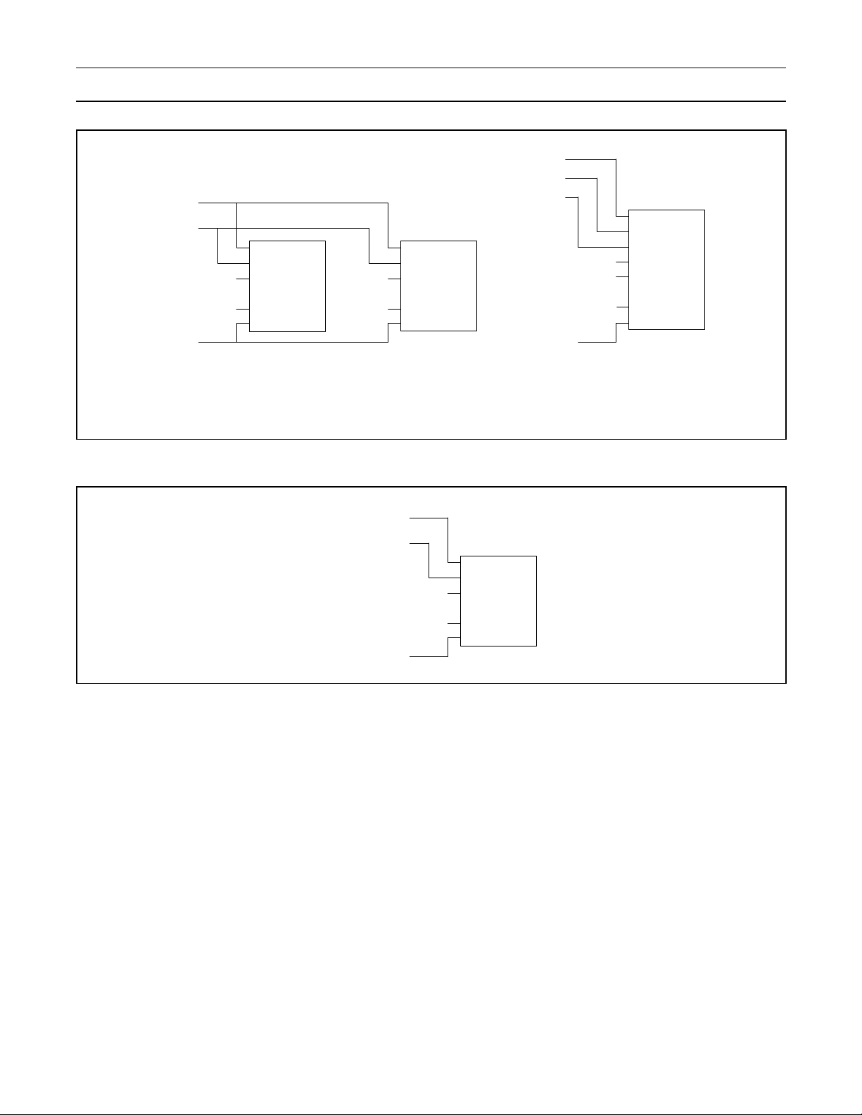
Philips Semiconductors Preliminary User Manual
LPC2119/2129/2292/2294ARM-based Microc ontroller
CS
OE
CS
OE
BLS[1]
CE
OE
WE
BLS[0]
CE
OE
WE
WE
BLS[1]
BLS[0]
CE
OE
WE
UB
LB
D[15:8]
IO[7:0]
A[a_m:0]
A[a_b:1]
a) 16 bit wide memory bank interfaced
to 8 bit memory chips
Figure 8: 16 Bit Bank External Memory Interfaces
D[7:0]
IO[7:0]
A[a_m:0]
A[a_b:1]
a) 16 bit wide memory bank interfaced
to 16 bit memory chips
CS
OE
CE
OE
BLS[0]
D[7:0]
WE
IO[7:0]
A[a_m:0]
A[a_b:0]
Figure 9: 8 Bit Bank External Memory Interface
D[15:0]
IO[15:0]
A[a_m:0]
External Memory Controller (EMC) 44 January 08, 2004
Page 45
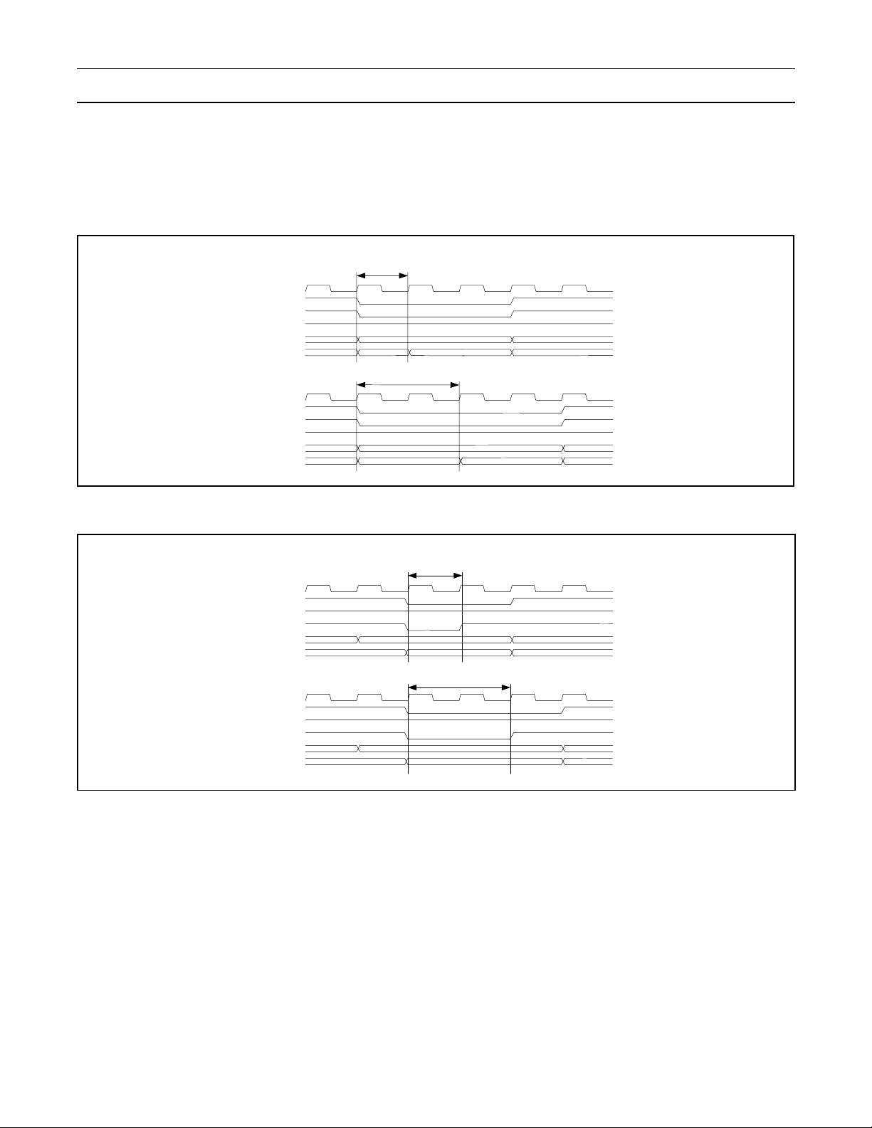
Philips Semiconductors Preliminary User Manual
LPC2119/2129/2292/2294ARM-based Microc ontroller
TYPICAL BUS SEQUENCES
Following figures show typical external read and write access cycles. XCLK is the clock signal avalable on P3.23. While not
necessary used by extern al m em ory , In the se examp les it is use d to p rov ide tim e refe renc e (XCLK a nd PC LK were set to have
the same frequency).
1 wait state (WST1=0)
XCLK
CS
OE
WE/BLS
Addr
Data
XCLK
CS
OE
WE/BLS
Addr
Data
valid address
change valid data
2 wait states (WST1=1)
valid address
change valid data
Figure 10: External memory read access (WST1=0 and WST1=1 examples)
WST2=0
XCLK
CS
OE
WE/BLS
Addr
Data
XCLK
CS
OE
WE/BLS
Addr
Data
valid address
valid data
WST2=1
valid address
valid data
Figure 11: External memory write access (WST2=0 and WST2=1 examples)
Figure 10 and Figure 11 are showing typ ical read an d write acc esses to exte rnal memo ry. Howeve r, variation s can be noti ced in
some particular cases.
For example, when the first read access to the memory bank that has just been selected is performed, CS and OE lines may
become low one XCLK cycle earlier than it is shown in Figure 10.
Likewise, in a sequenc e of several consec utive write accesse s to SRAM, the last write acce ss will look like th ose shown in Figure
11. On the other ha nd, lea ding write cycles i n th at case will have data valid one cy cl e l ong er. Also, isloated write access will be
identical to the one in Figure 11.
External Memory Controller (EMC) 45 January 08, 2004
Page 46

Philips Semiconductors Preliminary User Manual
LPC2119/2129/2292/2294ARM-based Microc ontroller
EXTERNAL MEMORY SELECTION
Based on the des cription of the EMC opera tion and ex ternal memo ry in genera l (appropriate read and write access t imes tAA and
t
respecitely), the fo llowing table ca n be cons tructed an d used for ex ternal me mory sel ection. t
WRITE
XCLK cycle (see Figure 10 and Figure 11). f
is the maximum pclk frequency achivable in the system with selected external
max
memory.
Table 10: External memory and system requirements
is the period of a single
CYC
Access
cycle
Standard
Read
Standard
Write
Max. frequency
2 + WST1
<= ———————
f
max
t
RAM
+ 20ns
1 + WST2
<= ———————
f
max
t
RAM
+ 5ns
WST setting
(WST>=0; round up to integer)
WST1>=
t
WST2>=
t
—————————
t
+ 20ns
RAM
—————— - 2
t
CYC
- t
WRITE
CYC
CYC
+ 5ns
Required memory access time
t
RAM
t
WRITE
<= t
*(2+WST1) - 20ns
CYC
<= t
*(1+WST2) - 5ns
CYC
External Memory Controller (EMC) 46 January 08, 2004
Page 47

Philips Semiconductors Preliminary User Manual
LPC2119/2129/2292/2294ARM-based Microc ontroller
External Memory Controller (EMC) 47 January 08, 2004
Page 48
Philips Semiconductors Preliminary User Manual
LPC2119/2129/2292/2294ARM-based Microc ontroller
4. SYSTEM CONTROL BLOCK
SUMMARY OF SYSTEM CONTROL BLOCK FUNCTIONS
The System Control Block includes several system features and control registers for a number of functions that are not related
to specific peripheral devices. These include:
• Crystal Oscillator.
• External Interrupt Inputs.
• Memory Mapping Control.
•PLL.
• Power Control.
•Reset.
• VPB Divider.
• Wakeup Timer.
Each type of fu nction has it s own reg ister(s) if any are required and unnee ded bits a re define d as reserved i n order to allow future
expansion. Unrelated functions never share the same register addresses.
PIN DESCRIPTION
Table 11 shows pins that are associated with System Control block functions.
Table 11: Pin summary
Pin name Pin direction Pin Description
X1 Input Crystal Oscillator Input- Input to the oscillator and internal clock generator circuits .
X2 Output Crystal Oscillator Output- Output from the oscillator amplifier.
External Interrupt Input 0- An ac tive low gene ral purpose interru pt input. This pin may be
used to wake up the processor from Idle or Power down modes.
EINT0 Input
EINT1 Input External Interrupt Input 1- See the EINT0 description above.
EINT2 Input External Interrupt Input 2- See the EINT0 description above.
EINT3 Input External Interrupt Input 3- See the EINT0 description above.
R
ESET Input
LOW level on this pin immediately after reset is considered as an external hardware
request to start the ISP command ha ndler. More de tails on ISP and Flash memory can be
found in "Flash Memory System and Programming" chapter.
External Reset input- A low on this pin resets the chi p, causing I/O ports and periphe rals
to take on their default states, and the processor to begin execution at address 0.
System Control Block 48 January 08, 2004
Page 49
Philips Semiconductors Preliminary User Manual
LPC2119/2129/2292/2294ARM-based Microc ontroller
REGISTER DESCRIPTION
All registers, regardless of size, are on word address boundaries. Details of the registers appear in the description of each
function.
Table 12: Summary of System Control Registers
Address Name Description Access
External Interrupts
0xE01FC140 EXTINT External Interrupt Flag Register. R/W 0
0xE01FC144 EXTWAKE External Interrupt Wakeup Register. R/W 0
0xE01FC148 EXTMODE External Interrupt Flag Register. R/W 0
0xE01FC14C EXTPOLAR External Interrupt Wakeup Register. R/W 0
Memory Mapping Control
0xE01FC040 MEMMAP Memory Mapping Control. R/W 0
Phase Locked Loop
0xE01FC080 PLLCON PLL Control Register. R/W 0
0xE01FC084 PLLCFG PLL Configuration Register. R/W 0
0xE01FC088 PLLSTAT PLL Status Register. RO 0
0xE01FC08C PLLFEED PLL Feed Register. WO NA
Power Control
0xE01FC0C0 PCON Power Control Register. R/W 0
0xE01FC0C4 PCONP Power Control for Peripherals. R/W 0x3BE
VPB Divider
0xE01FC100 VPBDIV VPB Divider Control. R/W 0
Reset
Value*
*Reset Value refers to the data stored in used bits only. It does not include reserved bits content.
System Control Block 49 January 08, 2004
Page 50
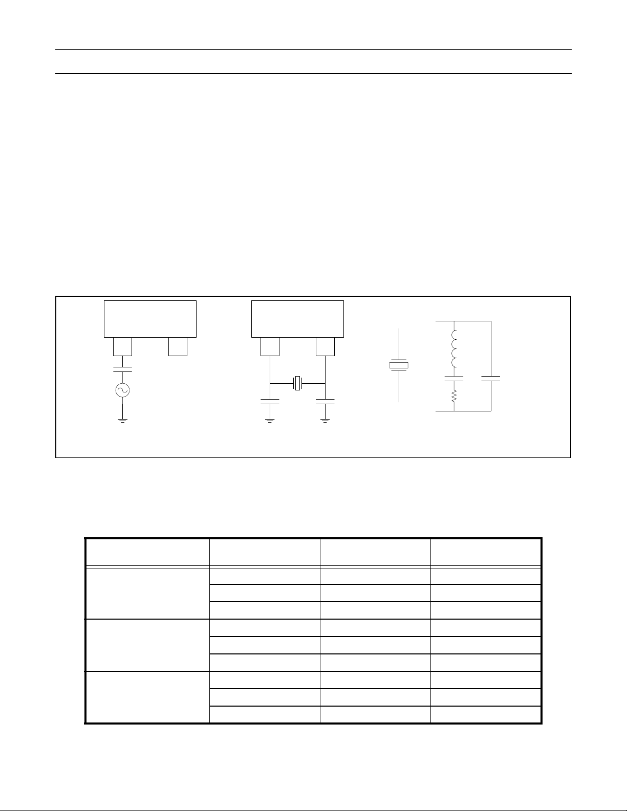
Philips Semiconductors Preliminary User Manual
LPC2119/2129/2292/2294ARM-based Microc ontroller
CRYSTAL OSCILLATOR
The oscillator supports crystals in the range of 10 MHz to 25 MHz. The oscillator output frequency is called F
processor clock frequency is referred to as cclk for purposes of rate equations, etc. elsewhere in this document. F
and the ARM
osc
and cclk
osc
are the same value unless the PLL is running and connected. Refer to the PLL description in this chapter for details.
Onboard oscillator in LPC2119/2129/2292/2294 can operate in one of two modes: slave mode and oscillation mode.
In slave mode the input cloc k si gna l sho uld be cou pled by means of a capacitor of 100 pF (Cc in Figu re 12, draw in g a), wi th an
amplitude of at least 200 mVrms. X2 pin in this configuration can be left not connected.
External components and models use d in oscillatio n mode are shown in Figure 12, drawings b and c, an d in Table 13. Sinc e the
feedback resistance is integrated on chip, only a crystal and the capacitances C
case of fundamental mod e oscillatio n (the fundamenta l frequency is repr esented by L, C
drawing c, represents the par all el pa ck age capacitance and should not be large r than 7 pF. Para me ters F
and CX2 need to be connected externally in
X1
and RS). Capacitance Cp in Figure 12,
L
, CL, RS and CP are
C
supplied by the crystal manufa ctu rer.
LPC2119/2129
LPC2292/2294
X1 X2
C
C
Clock
LPC2119/2129
LPC2292/2294
X1 X2
C
X1
Xtal
L
<=>
C
L
R
C
X2
S
C
P
a) b) c)
Figure 12: Oscillator modes and models: a) slave mode of operation, b) oscillation mode of operation,
c) external crystal model used for C
Table 13: Recommended values for C
Fundamental Oscillation
Frequency F
C
Crystal Load
Capacitance C
10 - 15 MHz
15 - 20 MHz
20 - 25 MHz
when oscillation mode is used
X1/X2
Max. Crystal Series
L
Resistence R
10 pF < 300 Ω 18 pF, 18 pF
20 pF < 220 Ω 38 pF, 38 pF
30 pF < 140 Ω 58 pF, 58 pF
10 pF < 220 Ω 18 pF, 18 pF
20 pF < 140 Ω 38 pF, 38 pF
30 pF < 80 Ω 58 pF, 58 pF
10 pF < 160 Ω 18 pF, 18 pF
20 pF < 90 Ω 38 pF, 38 pF
30 pF < 50 Ω 58 pF, 58 pF
X1/X2
evaluation
S
External Load
Capacitors C
X1
, C
X2
System Control Block 50 January 08, 2004
Page 51
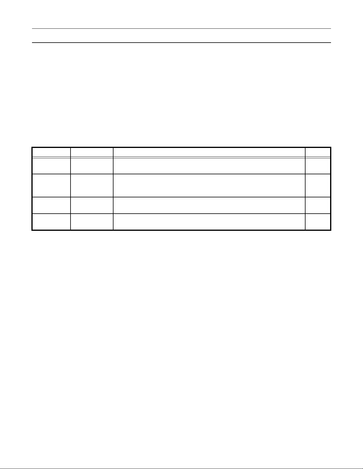
Philips Semiconductors Preliminary User Manual
LPC2119/2129/2292/2294ARM-based Microc ontroller
EXTERNAL INTERRUPT INPUTS
The LPC2119/2129/2292/2294 includes four External Interrupt Inputs as selectable pin functions. The External Interrupt Inputs
can optionally be used to wake up the processor from the Power Down mode.
Register Description
The external interrupt function has four registers associated with it. The EXTINT register contains the interrupt flags, and the
EXTWAKEUP register contains bits that enable individual external interrupts to wake up the LPC2119/2129/2292/2294 from
Power Down mode. The EXTMODE and EXTPOLAR registers specify the level and edge sensitivity parameters.
Table 14: External Interrupt Registers
Address Name Description Access
0xE01FC140 EXTINT
0xE01FC144 EXTWAKE
0xE01FC148 EXTMODE
0xE01FC14C EXTPOLAR
The External Interrupt Flag Register contains interrupt flags for EINT0, EINT1,
and EINT2. See Table 15.
The External Interrupt Wakeup Register contains three enable bits that control
whether each external inte rrupt will cause the processor to wake up from Power
Down mode. See Table 16.
The External Interrupt Mode R egister co ntrols whethe r each pin is edge- or levelsensitive.
The External Interrupt Polarity Regi ster control s which leve l or edge on ea ch pin
will cause an interrupt.
R/W
R/W
R/W
R/W
External Interrupt Flag Register (EXTINT - 0xE01FC140)
When a pin is selected for its external interrupt function , the le ve l or ed ge on t hat pi n se le cte d by its bi ts i n the EXT POL AR and
EXTMODE registers will set its interrupt flag in this register. This asserts the corresponding interrupt request to the VIC, which
will cause an intrerrupt if interrupts from the pin are enabled.
Writing ones to bits EINT0 thr ough EINT3 in EXTINT register cl ears the corre sponding bits. In level- sensitive m ode this action is
efficacious only when the pin is in its innactive state.
System Control Block 51 January 08, 2004
Page 52
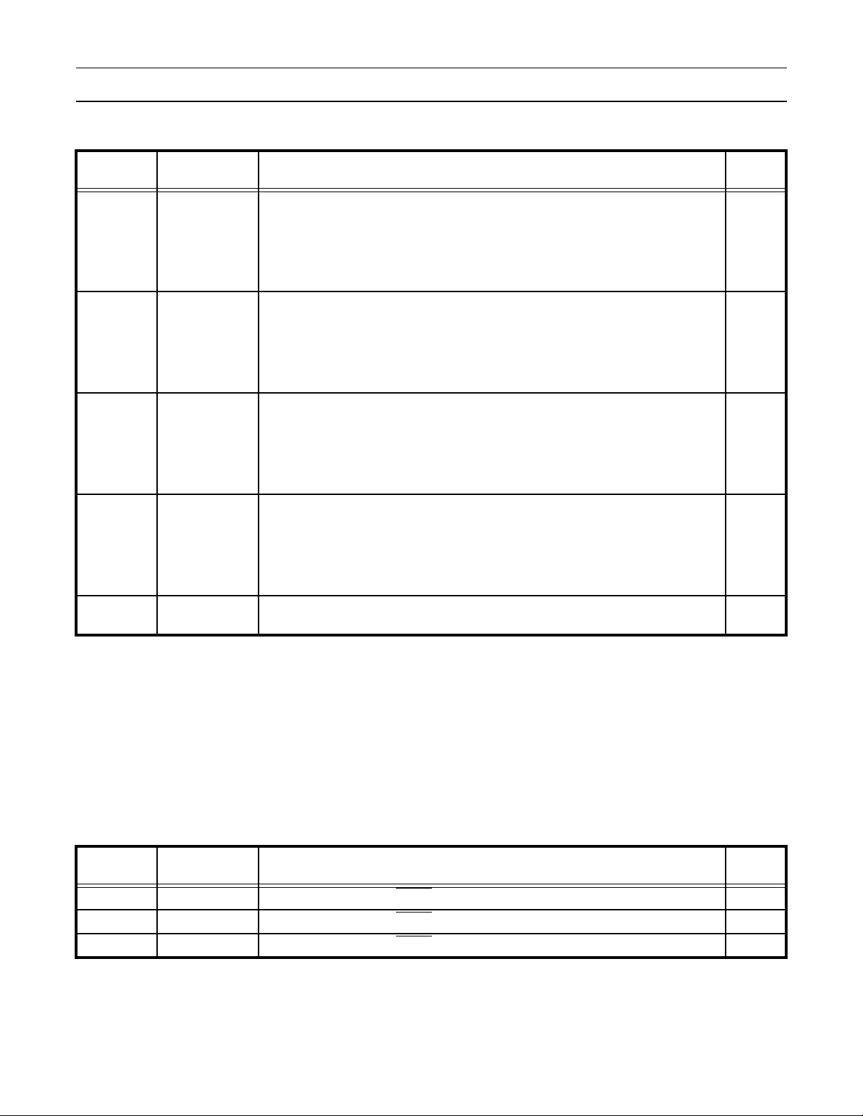
Philips Semiconductors Preliminary User Manual
LPC2119/2129/2292/2294ARM-based Microc ontroller
Table 15: External Interrupt Flag Register (EXTINT - 0xE01FC140)
EXTINT Function Description
In level-sensitive mode, this bit is set i f the EINT0 func tion is selec ted for its p in, and
the pin is in its active state. In edge-sensitive mode, this bit is set if the EINT0
0EINT0
1EINT1
2EINT2
3EINT3
7:4 Reserved
function is selected for its pin, and the selected edge occurs on the pin.
This bit is cleared by writi ng a one to it, except in level sensitiv e mode when the pi n
is in its active state.
In level-sensitive mode, this bit is set i f the EINT1 func tion is selec ted for its p in, and
the pin is in its active state. In edge-sensitive mode, this bit is set if the EINT1
function is selected for its pin, and the selected edge occurs on the pin.
This bit is cleared by writi ng a one to it, except in level sensitiv e mode when the pi n
is in its active state.
In level-sensitive mode, this bit is set i f the EINT2 func tion is selec ted for its p in, and
the pin is in its active state. In edge-sensitive mode, this bit is set if the EINT2
function is selected for its pin, and the selected edge occurs on the pin.
This bit is cleared by writi ng a one to it, except in level sensitiv e mode when the pi n
is in its active state.
In level-sensitive mode, this bit is set i f the EINT3 func tion is selec ted for its p in, and
the pin is in its active state. In edge-sensitive mode, this bit is set if the EINT3
function is selected for its pin, and the selected edge occurs on the pin.
This bit is cleared by writi ng a one to it, except in level sensitiv e mode when the pi n
is in its active state.
Reserved, user software should not write ones to reserved bits. The value read
from a reserved bit is not defined.
Reset
Value
0
0
0
0
NA
External Interrupt Wakeup Register (EXTWAKE - 0xE01FC144)
Enable bits in the EXTWAKE register allow the external interrupts to wake up the processor if it is in Power Down mode. The
related EINTn function must be mapped to the pin in order for the wakeup process to take place. It is not necessary for the
interrupt to be enabled in the Vectored Interrupt Controller for a wakeup to take place. This arrangement allows additional
capabilities, such as having an external interrupt input wake up the processor from Power Down mode without causing an
interrupt (simply resuming operation), or allowing an interrupt to be enabled during Power Down without waking the processor
up if it is asserted (eliminating the need to disable the interrupt if the wakeup feature is not desirable in the application).
Table 16: External Interrupt Wakeup Register (EXTWAKE - 0xE01FC144)
EXTWAKE Function Description
0 EXTWAKE0 When one, assertion of EINT0
1 EXTWAKE1 When one, assertion of EINT1
2 EXTWAKE2 When one, assertion of EINT2
will wake up the processor from Power Down mode. 0
will wake up the processor from Power Down mode. 0
will wake up the processor from Power Down mode. 0
System Control Block 52 January 08, 2004
Reset
Value
Page 53
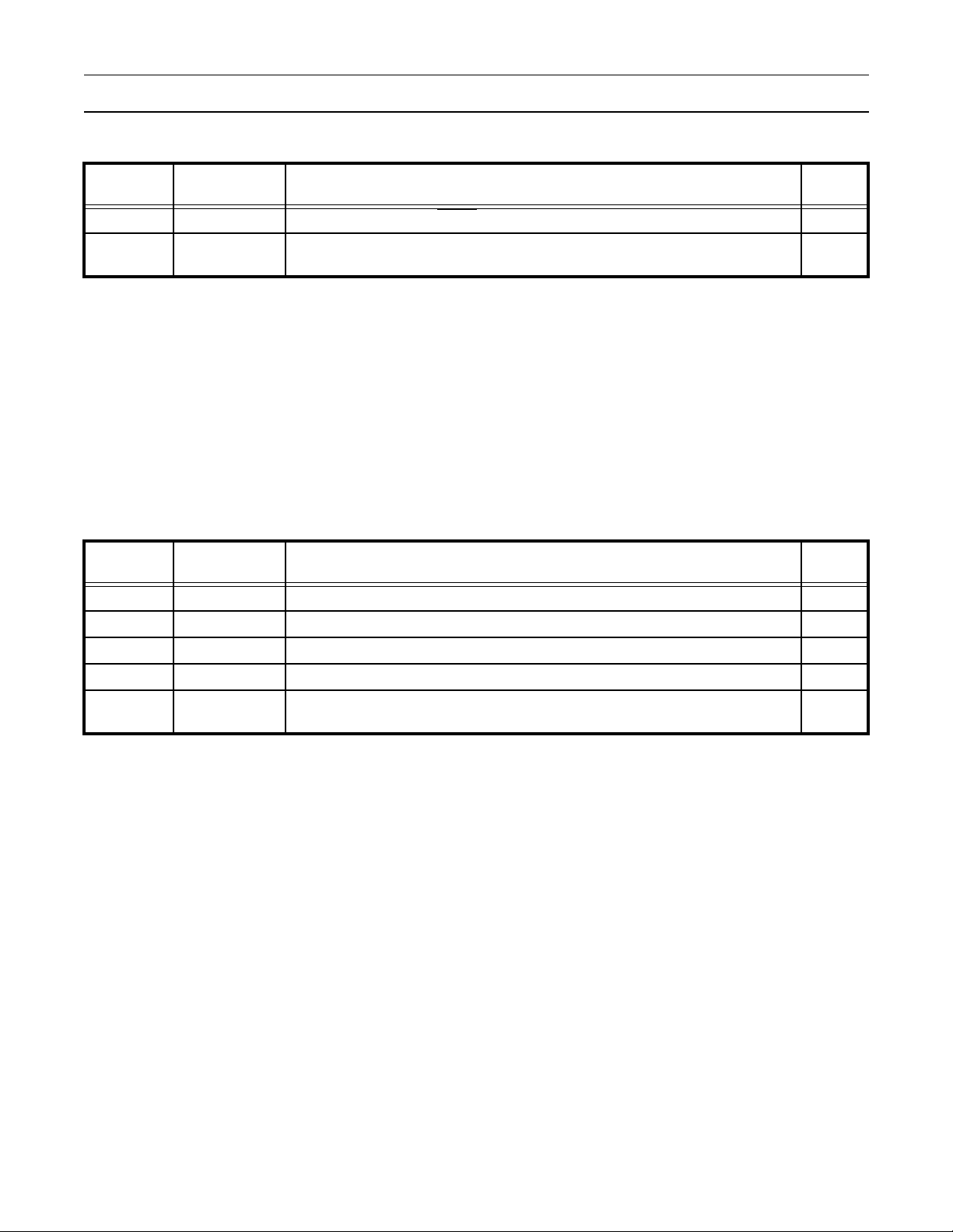
Philips Semiconductors Preliminary User Manual
LPC2119/2129/2292/2294ARM-based Microc ontroller
Table 16: External Interrupt Wakeup Register (EXTWAKE - 0xE01FC144)
EXTWAKE Function Description
3 EXTWAKE3 When one, assertion of EINT
7:4 Reserved
Reserved, user software should not write ones to reserved bits. The value read
from a reserved bit is not defined.
3 will wake up the processor from Power Down mode. 0
Reset
Value
NA
External Interrupt Mode Register (EXTMODE - 0xE01FC148)
The bits in thi s registe r select whether ea ch EINT pin is level- o r edge -sensitive. Only p ins that are sel ected for the EINT function
(chapter Pin Connec t Block on pa ge 100) an d enabled via the VI CIntEnabl e register (chapter Ve ctored Inte rrupt Control ler (VIC)
on page 76) can cause interrupts from the External Interrupt function (though of course pins selected for ) other functions may
cause interrupts from those funct ion s).
Note: Software should only change a bit in this regis ter when its interrupt is dis abled in VICIntEnable, and sh ould write
the corresponding 1 to EXTINT before re-enabling the interrupt, to clear the EXTINT bit that could be set by changing
the mode.
Table 17: External Interrupt Mode Register (EXTMODE - 0xE01FC148)
EXTMODE Function Description
0 EXTMODE0 When 0, level-sensitivity is selected for EINT0. When 1, EINT0 is edge-sensitive. 0
1 EXTMODE1 When 0, level-sensitivity is selected for EINT1. When 1, EINT1 is edge-sensitive. 0
Reset
Value
2 EXTMODE2 When 0, level-sensitivity is selected for EINT2. When 1, EINT2 is edge-sensitive. 0
3 EXTMODE3 When 0, level-sensitivity is selected for EINT3. When 1, EINT3 is edge-sensitive. 0
7:4 Reserved
Reserved, user software should not write ones to reserved bits. The value read
from a reserved bit is not defined.
NA
External Interrupt Polarity Register (EXTPOLAR - 0xE01FC14C)
In level-sensitive mode, the bits in this register select whether the corresponding pin is high- or low-active. In edge-sensitive
mode, they select whether the pin is rising- or falling-edge sensitive. Only pins that are selected for the EINT function (chapter
Pin Connect Block on page 100) a nd e nab led in the VICIntEnable registe r (ch apter Vectored Interrupt Controll er (VIC) o n pag e
76) can cause interrupts from the External Interrupt function (though of course pins selected for other functions may cause
interrupts from those functions ).
Note: Software should only change a bit in this regis ter when its interrupt is dis abled in VICIntEnable, and sh ould write
the corresponding 1 to EXTINT before re-enabling the interrupt, to clear the EXTINT bit that could be set by changing
the polarity.
System Control Block 53 January 08, 2004
Page 54
Philips Semiconductors Preliminary User Manual
LPC2119/2129/2292/2294ARM-based Microc ontroller
Table 18: External Interrupt Polarity Register (EXTPOLAR - 0xE01FC14C)
EXTPOLAR Function Description
0 EXTPOLAR0
1 EXTPOLAR1
2 EXTPOLAR2
3 EXTPOLAR3
7:4 Reserved
When 0, EINT0 is low-active or falling-edge sensitive (depending on EXTMODE0).
When 1, EINT0 is high-active or rising-edge sensitive (depending on EXTMODE0).
When 0, EINT1 is low-active or falling-edge sensitive (depending on EXTMODE1).
When 1, EINT1 is high-active or rising-edge sensitive (depending on EXTMODE1).
When 0, EINT2 is low-active or falling-edge sensitive (depending on EXTMODE2).
When 1, EINT2 is high-active or rising-edge sensitive (depending on EXTMODE2).
When 0, EINT3 is low-active or falling-edge sensitive (depending on EXTMODE3).
When 1, EINT3 is high-active or rising-edge sensitive (depending on EXTMODE3).
Reserved, user softw are should n ot write o nes to reser ved bits . The valu e read from
a reserved bit is not defined.
Reset
Value
0
0
0
0
NA
Multiple Ext er n a l In t e rrupt Pins
Software can select multiple pins for each of EINT3:0 in the Pin Select registers, which are described in chapter Pin Connect
Block on page 100. The external inte rrupt logic for each of EINT3:0 recei ves the state of all of its associated pin s from the p ins’
receivers, alon g with signals th at indic ate wh ether eac h pin is selected for the EINT func tion. Th e externa l interrup t logic handles
the case when more than one pin is so selected, differently according to the state of its Mode and Polarity bits:
• In Low-Active Le vel Sensitiv e mode, the stat es of all p ins select ed for EINT functi onality ar e digitally co mbined u sing a positive
logic AND gate.
• In High-Active Le vel Sensitive mode , the states of all p ins selected fo r EINT functionali ty are digitally c ombined using a po sitive
logic OR gate.
• In Edge Sensitive mode, regardless of polarity, the pin with the lowest GPIO port number is used. (Selecting multiple EINT pins
in edge-sensitive mode co uld be considered a programming error.)
The signal derived by this logic is the EINTi signal in the following logic schematic (Figure 13).
When more than one EINT pi n is logically ORed , the interrupt servic e routine can read the s tates of the pins from G PIO port using
IOPIN0 and IOPIN1 registers, to determine which pin(s) caused the interrupt.
System Control Block 54 January 08, 2004
Page 55
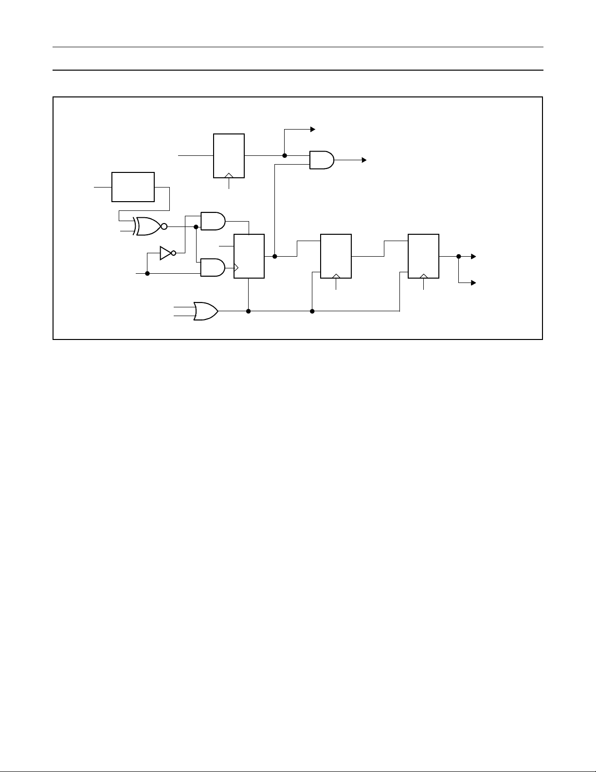
Philips Semiconductors Preliminary User Manual
LPC2119/2129/2292/2294ARM-based Microc ontroller
EINTi
EXTPOLARi
EXTMODEi
Write 1 to EXTINTi
VPB Bus Data
Glitch
Filter
Reset
Wakeup Enable
(one bit of EXTWAKE)
QD
pclk
1
S
D
Q
R
Figure 13: External Interrupt Logic
VPB Read
of EXTWAKE
EINTi to
Wakeup Timer
(Figure 15)
Interrupt Flag
(one bit of EXTINT)
S
Q
R
pclk pclk
S
Q
R
to VIC
VPB Read
of EXTINT
System Control Block 55 January 08, 2004
Page 56

Philips Semiconductors Preliminary User Manual
LPC2119/2129/2292/2294ARM-based Microc ontroller
MEMORY MAPPING CONTROL
The Memory Mapping Control alters the mapping of the interrupt vectors that appear beginning at address 0x00000000. This
allows code running in different memory spaces to have control of the interrupts.
Memory Mapping Control Register (MEMMAP - 0xE01FC040)
Table 19: MEMMAP Register
Address Name Description Access
0xE01FC040 MEMMAP
Table 20: Memory Mapping Control Register (MEMMAP - 0xE01FC040)
MEMMAP Function Description
1:0 MAP1:0
7:2 Reserved
*: The hardware reset value of the MAP bits is 00 for LPC2119/2129/2292/ 2294 parts. Th e apparent reset value that the user will
see will be altered by the Boot Loader code, which always runs initially at reset. User documentation will reflect this difference.
Memory mapping control. Selects whether the ARM interrupt vectors are read
from the Flash Boot Block, User Flash or RAM.
00: Boot Loader Mode. Interrupt vectors are re-mapped to Boot Block.
01: User Flash Mode. Interrupt vectors are not re-mapped and reside in Flash.
10: User RAM Mode. Interrupt vectors are re-mapped to Static RAM.
11: User External memory Mode. Interr upt vectors a re re-mapped to e xternal memory.
This mode is available in L2292/2294 only and must not be specified when
LPC2119/2129 are used.
Warning: Improper set tin g of t his v alue may result in inco rrect o perati on of the devi ce.
Reserved, user software shou ld not write ones to reserved b its. The value rea d from a
reserved bit is not defined.
R/W
Reset
Value*
0
NA
Memory Mapping Control Usage Notes
Memory Mapping Cont rol simply selects one out of three available sources of data (sets of 64 bytes each) nec essary for handli ng
ARM exceptions (interrupts).
For example, whenever a Software Interrupt request is generated, ARM core will always fetch 32-bit data "residing" on 0x0000
0008 (see Table 3, “ARM Exception Vector Locat ions,” on page 36). This mea ns that when MEMMAP[1:0]= 10 (User RAM Mode),
read/fetch from 0x0000 0008 will provide data stored in 0x4000 0008. If MEMMAP[1:0]=01 (User Flash Mode), read/fetch from
0x0000 0008 will provi de data st ored in on-c hip Flash locatio n 0x000 0 0008. In c ase of MEM MAP[1:0] =00 (Boot Lo ader Mod e),
read/fetch from 0x0000 00 08 will provid e data availbl e also at 0x7FFF E00 8 (Boot Block re mapped from on-chip Flash memory).
System Control Block 56 January 08, 2004
Page 57

Philips Semiconductors Preliminary User Manual
LPC2119/2129/2292/2294ARM-based Microc ontroller
PLL (PHASE LOCKED LOOP)
The PLL accepts an input clock frequency in the range of 10 MHz to 25 MHz. The input frequency is multiplied up into the cclk
with the range of 10 MHz to 60 MHz using a Current Controlled Oscillator (CCO). The multiplier can be an integer value from 1
to 32 (in practice , the mult ipl ier va lue ca nnot b e high er than 6 o n the LP C2119/21 29/229 2/2294 du e to the upper frequen cy limi t
of the CPU). The CCO operates in the range of 156 MHz to 320 MHz, so there is an additional divider in the loop to keep the
CCO within its f requency range while t he PLL is pro vi din g the desired output f requ enc y . Th e o utput divider may be s et to d iv ide
by 2, 4, 8, or 16 to pro du ce the output clock. Since the mi nim um o utpu t di vider value is 2, it is insured that the PLL outp ut has a
50% duty cycl e. A block diagram of the PLL is shown in Fi gure 14.
PLL activation is con trolled via the PLLC ON register. The PLL mu ltiplier and divider v alues are controlle d by the PLLCFG register.
These two registers are protected in order to prevent accidental alteration of PLL parameters or deactivation of the PLL. Since
all chip operations, including the Watchdog Timer, are dependent on the PLL when it is providing the chip clock, accidental
changes to the PLL setup could result in unexpected behavior of the microcontroller. The protection is accomplished by a feed
sequence similar to that of the Watchdog Timer. Details are provided in the description of the PLLFEED register.
The PLL is turned off and bypassed fol lowing a chip Reset and when by entering pow er Down mode. PLL is enabled by software
only. The program must configure and activate the PLL, wait for the PLL to Lock, then connect to the PLL as a clock source.
Register Description
The PLL is controlled by the registers shown in Table 21. More detailed descriptions follow.
Warning: Improper setting of PLL values may result in incorrect operation of the device.
Table 21: PLL Registers
Address Name Description Access
PLL Control Register. Holding register for updating PLL control bits. Values
0xE01FC080 PLLCON
0xE01FC084 PLLCFG
0xE01FC088 PLLSTAT
0xE01FC08C PLLFEED
written to this register do not take effect until a valid PLL feed sequ ence has taken
place.
PLL Configuration Register. Holding register for updating PLL configuration
values. Values written to this register do not take effect until a valid PLL feed
sequence has taken place.
PLL Status Register. Read-back register for PLL control and configuration
information. If PLLCON or PLLCFG have been written to, but a PLL feed
sequence has not yet occurred, they will not reflect the current PLL state.
Reading this registe r provides the actual val ues controlling the PL L, as well as the
status of the PLL.
PLL Feed Register. This register enables loading of the PLL control and
configuration information from the PLLCON and PLLCFG registers into the
shadow registers that actually affect PLL operation.
R/W
R/W
RO
WO
System Control Block 57 January 08, 2004
Page 58
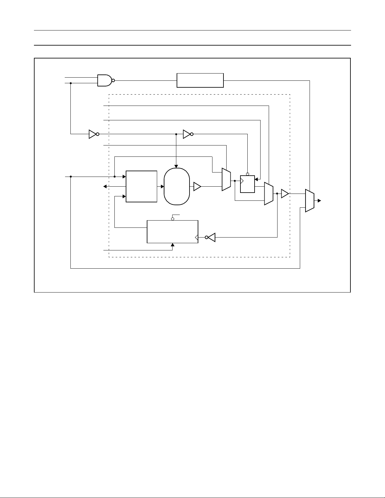
Philips Semiconductors Preliminary User Manual
LPC2119/2129/2292/2294ARM-based Microc ontroller
PLLC
PLLE
F
OSC
PSEL[1:0]
PLOCK
MSEL[4:0]
Clock
Synchronization
Direct
0
pd
pd
Bypass
0
Phase-
Frequency
Detector
CCO
F
CCO
1
0
cd
/2P
0
1
0
cclk
1
pd
fout
cd
Div-by-M
msel<4:0>
Figure 14: PLL Block Diagram
PLL Control Register (PLLCON - 0xE01FC080)
The PLLCON register contains the bits that enable and connect the PLL. Enabling the PLL allows it to attempt to lock to the
current settings of th e m ul tipl ier and divider value s. Conn ecting the PLL causes the processor and all chip func ti ons to run from
the PLL output clock. Changes to the PLLCO N register d o not take effect until a co rrect PLL fee d sequen ce has be en given (se e
PLL Feed Register (PLLFEED - 0xE01FC08C) description).
System Control Block 58 January 08, 2004
Page 59

Philips Semiconductors Preliminary User Manual
LPC2119/2129/2292/2294ARM-based Microc ontroller
Table 22: PLL Control Register (PLLCON - 0xE01FC080)
PLLCON Function Description
0 PLLE
1 PLLC
7:2 Reserved
The PLL must be set up, enabled, and Lock established before it may be used as a clock source. When switching from the
oscillator clock to the PLL output or vice versa, internal circuitry synchronizes the operation in order to ensure that glitches are
not generated. Hardw are does not insu re that the PLL is lo cked bef ore it is c onnected or autom atically di sconnec t the PLL i f lock
is lost during opera tion. In the event of l oss of PLL lock, it i s likely that the o scillator clock has become uns table and disconnecting
the PLL will not remedy the situation.
PLL Enable. When one, and after a valid PLL feed, this bit will activate the PLL and
allow it to lock to the requested frequency. See PLLSTAT register, Table 24.
PLL Connect. When PLLC and PLLE are both set to one, and after a valid PLL feed,
connects the PLL as the clock source for the LPC2119/2129/2292/2294. Otherwise,
the oscillator clock is used directly by the LPC2119/2129/2292/2294. See PLLSTAT
register, Table 24.
Reserved, user software shou ld not write ones to reserved b its. The value rea d from a
reserved bit is not defined.
Reset
Value
0
0
NA
PLL Configuration Register (PLLCFG - 0xE01FC084)
The PLLCFG register contains the PLL multiplier and divider values. Changes to the PLLCFG register do not take effect until a
correct PLL feed sequenc e has been giv en (see PLL Feed Re gister (PLLFEED - 0xE01FC08C) desc ription). Calcul ations for the
PLL frequency, and multiplier and divider values are found in the PLL Frequency Calculation section.
Table 23: PLL Configuration Register (PLLCFG - 0xE01FC084)
PLLCFG Function Description
4:0 MSEL4:0 PLL Multiplier value. Supplies the value "M" in the PLL frequency calculations. 0
6:5 PSEL1:0 PLL Divider value. Supplies the value "P" in the PLL frequency calculations. 0
7 Reserved
Reserved, user software shou ld not write ones to reserved b its. The value rea d from a
reserved bit is not defined.
Reset
Value
NA
PLL Status Register (PLLSTAT - 0xE01FC088)
The read-only PLLSTAT register provides the actual PLL parameters that are in effect at the time it is read, as well as the PLL
status. PLLSTAT may disa gree with values foun d in PLLCON and PLLCFG beca use changes to those re gisters do not take effe ct
until a proper PLL feed has occurred (see PLL Feed Register (PLLFEED - 0xE01FC08C) description).
System Control Block 59 January 08, 2004
Page 60
Philips Semiconductors Preliminary User Manual
LPC2119/2129/2292/2294ARM-based Microc ontroller
Table 24: PLL Status Register (PLLSTAT - 0xE01FC088)
PLLSTAT Function Description
4:0 MSEL4:0 Read-back for the PLL Multiplier value. This is the value currently used by the PLL. 0
6:5 PSEL1:0 Read-back for the PLL Divider value. This is the value currently used by the PLL. 0
7 Reserved
8 PLLE
9 PLLC
10 PLOCK
15:11 Reserved
PLL Interrupt
The PLOCK bit in the PLLSTAT register is connected to the interrupt controller. This allows for software to turn on the PLL and
continue with other fun ctions without having to wait for the PLL to ach ieve lock. Wh en the interru pt occurs (PLOCK = 1), the PLL
may be connected, and the interrupt disabled.
Reserved, user software shou ld not write ones to reserved bits. The value rea d from
a reserved bit is not defined.
Read-back for the PLL Enable bit. When one, the PLL is currently activated. When
zero, the PLL is turne d off. This bit is aut omatically cleared w hen Power Do wn mode
is activated.
Read-back for the PLL Conne ct bit. W hen PLLC an d PLL E are b oth one , the PLL is
connected as the clo ck source for the LPC 2119/2129/2 292/2294. Whe n either PLLC
or PLLE is zero, the PLL is bypassed and the oscillator clock is used directly by the
LPC2119/2129/2292/22 94. This bit is autom atically cleared w hen Power Down mode
is activated.
Reflects the PLL Lock status . When zero , the PLL is no t locked. Wh en one, the PLL
is locked onto the requested frequency.
Reserved, user software shou ld not write ones to reserved bits. The value rea d from
a reserved bit is not defined.
Reset
Value
NA
0
0
0
NA
PLL Modes
The combinations of PLLE and PLLC are shown in Table 25.
Table 25: PLL Control Bit Combinations
PLLC PLLE PLL Function
0 0 PLL is turned off and disconnected. The system runs from the unmodified clock input.
0 1 The PLL is active, but not yet connected. The PLL can be connected after PLOCK is asserted.
10
1 1 The PLL is active and has been connected as the system clock source.
Same as 0 0 combination. This preven ts the possibility of the PLL bei ng connected without als o being
enabled.
PLL Feed Register (PLLFEED - 0xE01FC08C)
A correct feed sequence mus t be written to the PLLFEED regi ster in o rder for chang es to the PLLCO N and PLLCFG reg isters to
take effect. The feed sequence is:
1. Write the value 0xAA t o PLLFEED
2. Write the value 0x55 to PLLFEED.
System Control Block 60 January 08, 2004
Page 61
Philips Semiconductors Preliminary User Manual
LPC2119/2129/2292/2294ARM-based Microc ontroller
The two writes must be in the correct sequence, and must be consecutive VPB bus cycles. The latter requirement implies that
interrupts must be disabled for the duration of the PLL feed operation. If either of the feed values is incorrect, or one of the
previously mentioned conditions is not met, any changes to the PLLCON or PLLCFG register will not become effective.
Table 26: PLL Feed Register (PLLFEED - 0xE01FC08C)
PLLFEED Function Description
7:0 PLLFEED
The PLL feed sequence must be written to this register in order for PLL
configuration and control register changes to take effect.
Reset
Value
undefined
PLL and Power Down Mode
Power Down mode automatically turns off and disconnects the PLL. Wakeup from Power Down mode does not automatically
restore the PLL settings, this must be done in software. Typically, a routine to activate the PLL, wait for lock, and then connect
the PLL can be called at the begin nin g of any i nterrupt service ro utin e that migh t be cal led due to the w akeup . It is import ant not
to attempt to restart the PLL by simply feeding it when execution resumes after a wakeup from Power Down mode. This would
enable and connect the PLL at the same time, before PLL lock is established.
PLL Frequency Calculation
The PLL equations use the following parameters:
F
OSC
F
CCO
cclk the PLL output frequency (also the processor clock frequency)
M PLL Multiplier value from the MSEL bits in the PLLCFG register
P PLL Divider value from the PSEL bits in the PLLCFG register
the frequency from the crystal oscillator
the frequency of the PLL current controlled oscillator
The PLL output frequency (when the PLL is both active and connected) is given by:
F
cclk = M * F
or cclk = ———
osc
cco
2 * P
The CCO frequency can be computed as:
F
= cclk * 2 * P or F
cco
cco
= F
* M * 2 * P
osc
The PLL inputs and settings must meet the following:
•F
is in the range of 10 MHz to 25 MHz.
osc
• cclk is in the range of 10 MHz to F
is in the range of 156 MHz to 320 MHz.
•F
cco
(the maximum allowed frequency for the LPC2119/2129/2292/2294).
max
System Control Block 61 January 08, 2004
Page 62
Philips Semiconductors Preliminary User Manual
LPC2119/2129/2292/2294ARM-based Microc ontroller
Procedure for Determining PLL Settings
If a particular application uses the PLL, its configuration may be determined as follows:
1. Choose the desired processor operating frequency (cclk). This may be based on processor throughput requirements,
need to support a spec ific set o f UART baud rates, etc. Be ar i n mind that periph eral d evices ma y be runnin g from a low er
clock than the processor (see the VPB Divider description in this chapter).
2. Choose an oscillator frequency (F
3. Calculate th e va lue of M to configure the MSE L bi ts. M = c cl k / F
to the MSEL bits in PLLCFG is M - 1 (see Table 28).
4. Find a value fo r P to con fig ure the PSEL b its, s uc h t hat F
the equation given abov e. P must have on e of the valu es 1, 2, 4, or 8. Th e value writt en to the PSEL bits in PL LCFG is 00
). cclk must be the whole (non-fractional) multiple of F
osc
. M must be in the rang e of 1 to 32 . Th e va lue w ritte n
osc
is within its defined frequency lim its. F
cco
for P = 1; 01 for P = 2; 10 for P = 4; 11 for P = 8 (see Table 27).
Table 27: PLL Divider Values
osc
.
is calculated us ing
cco
PSEL Bits
(PLLCFG bits 6:5)
00 1
01 2
10 4
11 8
Table 28: PLL Multiplier Values
MSEL Bits
(PLLCFG bits 4:0)
00000 1
00001 2
00010 3
00011 4
... ...
11110 31
11111 32
Valu e of P
Value of M
PLL Example
System design asks for F
Based on th ese specifications, M = cclk / F
Value for P can be derived from P = F
the lowest allowed fre quency for F
= 10 MHz and requires cclk = 60 MHz.
osc
= 60 MHz / 10 MHz = 6. Consequenty, M-1 = 5 will be written as PLLCFG 4:0.
osc
/ (cclk * 2), using condition that F
cco
= 156 MHz, P = 156 MHz / (2*60 MHz) = 1.3. The highest F
cco
must be in range of 156 MHz to 320 M Hz. Assuming
cco
frequency criteria prod uces
cco
P = 2.67. The only solut ion for P tha t sa tis fies both of these requirem ents and is listed in Table 27 is P = 2. Th ere fore , PLLCFG
6:5 = 1 will be used.
System Control Block 62 January 08, 2004
Page 63
Philips Semiconductors Preliminary User Manual
LPC2119/2129/2292/2294ARM-based Microc ontroller
POWER CONTROL
The LPC2119/2129/22 92/ 2294 suppo rts tw o redu ced p ower mo de s: Idl e mode a nd Power D own m ode. I n Idle mode , exec ution
of instructions is suspen ded until ei ther a Reset o r interrupt occurs. Peri pheral functi ons contin ue operation during Idle mode and
may generate interrupts to cause the processor to resume execution. Idle mode eliminates power used by the processor itself,
memory systems and related controllers, and internal buses.
In Power Down mode, the oscillator is shut down and the chip receives no internal clocks. The processor state and registers,
peripheral registers, and internal SRAM values are preserved throughout Power Down mode and the logic levels of chip pins
remain static. The Power Down mode can be terminated and normal operation resumed by either a Reset or certain specific
interrupts that are able to function without clocks. Since all dynamic operation of the chip is suspended, Power Down mode
reduces chip power consumption to nearly zero.
Entry to Power Down and Idle mode s must be coord inated with program execution. Wake up from Power Down or Id le modes via
an interrupt resumes program execu tion in such a w ay that no in structions are los t, incomplete, or repeated. Wake u p from Power
Down mode is discussed further in the description of the Wakeup Timer later in this chapter.
A Power Control for Peripherals feature allows individual peripherals to be turned off if they are not needed in the application,
resulting in additional power savings.
Register Description
The Power Control function contains two registers, as shown in Table 29. More detailed descriptions follow.
Table 29: Power Control Registers
Address Name Description Access
0xE01FC0C0 PCON
0xE01FC0C4 PCONP
Power Control Register. This register contains control bits that enable the two
reduced power operati ng modes of the L PC2119/2129 /2292/2294. See Ta ble 30.
Power Control for Peripherals Register. This register contains control bits that
enable and disable indiv idual pe riphera l functi ons, Allo wing elim inati on of pow er
consumption by peripherals that are not needed.
R/W
R/W
Power Control Register (PCON - 0xE01FC0C0)
The PCON register contai ns two bits. Writin g a one to the corres ponding bit ca uses entry to eithe r the Power Down or Idle mode.
If both bits are set, Power Down mode is entered.
Table 30: Power Control Register (PCON - 0xE01FC0C0)
PCON Function Description
Idle mode - when 1, this bit causes the processor clock to be stopped, while on-chip
0IDL
peripherals remain activ e. Any enabled interrupt from a peripheral or an ex ternal interrupt
source will cause the processor to resume execution.
Reset
Value
0
Power Down mode - when 1, this bit causes the oscillator and all on-chip clocks to be
1PD
7:2 Reserved
stopped. A wakeup condition from an external interrupt can cause the oscillator to restart, the PD bit to be cleared, and the processor to resume execution.
Reserved, user software should not write ones to reserved bits. The value read from a
reserved bit is not defined.
0
NA
System Control Block 63 January 08, 2004
Page 64
Philips Semiconductors Preliminary User Manual
LPC2119/2129/2292/2294ARM-based Microc ontroller
Power Control for Peripherals Register (PCONP - 0xE01FC0C4)
The PCONP register all ows turn ing off selec ted pe riphera l func tions for the p urpose of sa ving pow er. A few p eriphe ral fun ctions
cannot be turned off (i.e. the Watchdog tim er, GPIO, the Pin Connect blo ck , a nd the Sys te m Co ntro l block). Each bit in PCO N P
controls one of the peripherals. The bit numbers correspond to the related peripheral number as shown in the VPB peripheral
map in the LPC2119/2129/2292/2294 Memory Addressing section.
Table 31: Power Control for Peripherals Register for LPC2119/2129 (PCONP - 0xE01FC0C4)
PCONP Function Description
0 Reserved
1 PCTIM0 When 1, TIMER0 is enabled. When 0, TIMER0 is disabled to conserve power. 1
2 PCTIM1 When 1, TIMER1 is enabled. When 0, TIMER1 is disabled to conserve power. 1
3 PCURT0 When 1, UART0 is enabled. When 0, UART0 is disabled to conserve power. 1
4 PCURT1 When 1, UART1 is enabled. When 0, UART1 is disabled to conserve power. 1
5 PCPWM0 When 1, PWM0 is enabled. When 0, PWM0 is disabled to conserve power. 1
6 Reserved
7 PCI2C When 1, the I
8 PCSPI0 When 1, the SPI0 interf ace is enabled. When 0, the SPI0 is disabled to conserve powe r. 1
9 PCRTC When 1, the RTC is enabled. When 0, the RTC is disabled to conserve power. 1
10 PCSPI1 When 1, the SPI1 interface is enabled. When 0, the SPI1 is disabled to conserve power. 1
11 Reserved User software should write 0 here to reduce power consumption. 1
12 PCAD When 1, the A/D converter is enabled. When 0, the A/D is disabled to conserve power. 1
13 PCCAN1
Reserved, user software s hould not writ e ones to reserved bits . The value read fro m a reserve d
bit is not defined.
User software should not write ones to reserved bits. The value read from a reserved bit is not
defined.
2
C interface is enabled. When 0, the I2C interface is disabled to conserve power. 1
When 1, CAN Controller 1 is enabled. When 0, it is disabled to save power.
Note: the Acceptance Filter is enabled if any of CAN Controllers 1-2 is enabled.
Reset
Value
0
0
1
14 PCCAN2 When 1, CAN Controller 2 is enabled. When 0, it is disabled to save power. 1
31:15 Reserved
Table 32: Power Control for Peripherals Register for LPC2292/2294 (PCONP - 0xE01FC0C4)
PCONP Function Description
0 Reserved
1 PCTIM0 When 1, TIMER0 is enabled. When 0, TIMER0 is disabled to conserve power. 1
2 PCTIM1 When 1, TIMER1 is enabled. When 0, TIMER1 is disabled to conserve power. 1
3 PCURT0 When 1, UART0 is enabled. When 0, UART0 is disabled to conserve power. 1
Reserved, user software s hould not writ e ones to reserved bits . The value read fro m a reserve d
bit is not defined.
Reserved, user software s hould not writ e ones to reserved bits . The value read fro m a reserve d
bit is not defined.
NA
Reset
Value
0
System Control Block 64 January 08, 2004
Page 65

Philips Semiconductors Preliminary User Manual
LPC2119/2129/2292/2294ARM-based Microc ontroller
Table 32: Power Control for Peripherals Register for LPC2292/2294 (PCONP - 0xE01FC0C4)
PCONP Function Description
4 PCURT1 When 1, UART1 is enabled. When 0, UART1 is disabled to conserve power. 1
5 PCPWM0 When 1, PWM0 is enabled. When 0, PWM0 is disabled to conserve power. 1
6 Reserved
7 PCI2C When 1, the I
8 PCSPI0 When 1, the SPI0 interf ace is enabled. When 0, the SPI0 is disabled to conserve powe r. 1
9 PCRTC When 1, the RTC is enabled. When 0, the RTC is disabled to conserve power. 1
10 PCSPI1 When 1, the SPI1 interface is enabled. When 0, the SPI1 is disabled to conserve power. 1
11 PCEMC
12 PCAD When 1, the A/D converter is enabled. When 0, the A/D is disabled to conserve power. 1
13 PCCAN1
14 PCCAN2 When 1, CAN Controller 2 is enabled. When 0, it is disabled to save power. 1
15 PCCAN3 When 1, CAN Controller 3 is enabled. When 0, it is disabled to save power. 1
16 PCCAN4 When 1, CAN Controller 4 is enabled. When 0, it is disabled to save power. 1
User software should not write ones to reserved bits. The value read from a reserved bit is not
defined.
2
C interface is enabled. When 0, the I2C interface is disabled to conserve power. 1
When 1, the External Memory Controller is enable d. When 0, th e EMC is disabled to conserve
power.
When 1, CAN Controller 1 is enabled. When 0, it is disabled to save power.
Note: the Acceptance Filter is enabled if any of CAN Controllers 1-5 is enabled.
Reset
Value
0
1
1
17 PCCAN5 When 1, CAN Controller 5 is enabled. When 0, it is disabled to save power. 1
18 PCCAN6 When 1, CAN Controller 6 is enabled. When 0, it is disabled to save power. 1
31:19 Reserved
Reserved, user software s hould not writ e ones to reserved bits . The value read fro m a reserve d
bit is not defined.
0
System Control Block 65 January 08, 2004
Page 66
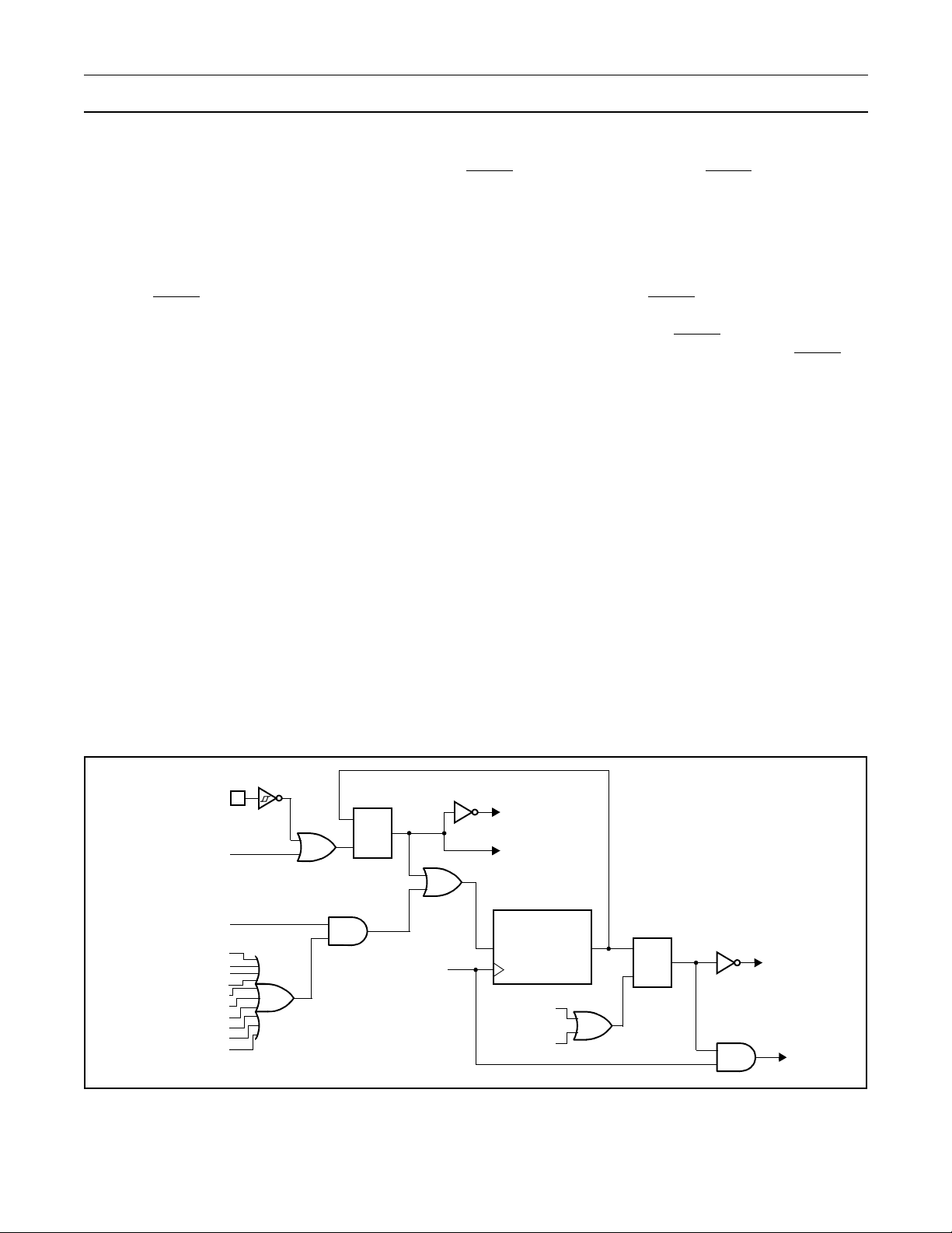
Philips Semiconductors Preliminary User Manual
LPC2119/2129/2292/2294ARM-based Microc ontroller
RESET
Reset has two sources on the LPC2119/2129/2292/2294: the RESET pin and Watchdog Reset. The RESET pin is a Schmitt
trigger input pin with an additional glitc h filter. Assertion of ch ip Reset by any so urce starts the Wak eup Timer (see Wakeup Timer
description later i n this chapter), caus ing reset to remain as serted until the ex ternal Reset is de- asserted, the osc illator is runnin g,
a fixed number of c loc ks h av e pas se d, and the Flash c ont roll er has c om pl ete d i ts initialization. The re lati ons hi p between Reset,
the oscillator, and the Wakeup Timer are shown in Figure 15.
The Reset glitch fi lter al lows th e proce ssor t o igno re exte rnal res et pul ses that a re very short , and al so de termin es the minim um
duration of R
when crystal oscillator is fully running and an adequate signal is present on the X1 pin of the LPC2119/2129/2292/2294.
Assuming that an external crystal is used in the crystal os cilla tor subs ystem , after power on, the R
for 10 ms. For all subsequent resets when crystal osillator is already running and stable signal is on the X1 pin, the R
needs to be asserted for 300 ns only.
ESET that must be asserted in order to guaran tee a chip reset. On ce asserted, RESET pin can be deasserted only
ESET pin should be asserted
ESET pin
Speaking in general, there are no sequence requirements for powering up the supplies (V
proper reset handli ng It is absolut ely necessary to have valid vol tage supply on V
dedicated hardware are powe red by the m. V
Consequently, not providing V
power supply will not affect the reset sequence itself, but will prevent microcontroller from
3
pins enable microcontroller’s interface to the environment via its digital pins.
3
pins, since on-chi p Reset circuit a nd oscillator
18
, V3, V
18
and V3A). However, for
18A
communicating with external world.
When the internal Reset is rem oved, the p rocessor be gins executin g at address 0, which is initially the Reset vector mappe d from
the Boot Block. At that point, all of the processor and peripheral registers have been initialized to predetermined values.
External and internal Resets have some small differences. An external Reset causes the value of certain pins to be latched to
configure the part. External circuitry cannot determine when an internal Reset occurs in order to allow setting up those special
pins, so those latches are not reloaded during an internal Reset. Pins that are examined during an external Reset for various
purposes are: P1.20/TRACESYNC, P1.26/RTCK, BOOT1 and BOOT0 (see chapters Pin Configuration on page 86, Pin Connect
Block on page 100 and Extern al Memory Controller (EMC) on page 40). Pin P0.14 (see Flash Me mory System and Program ming
on page 228) is exemined by on-chip bootloader when this code is executed after reset.
It is possible for a chip Reset to occur during a Flash programming or erase operation. The Flash memory will interrupt the
ongoing operation and hold off the completion of Reset to the CPU until internal Flash high voltages have settled.
External
Reset
Watchdog
Reset
C
Q
S
Reset to
kFlash shell
Reset to
PCON.PD
Power Down
EINT0 Wakeup
EINT1 Wakeup
EINT2 Wakeup
EINT3 Wakeup
CAN1 Wakeup
CAN2 Wakeup
CAN3 Wakeup*
CAN4 Wakeup*
CAN5 Wakeup*
CAN6 Wakeup*
*LPC2292/2294 only
Oscillator
Output (F
OSC
)
Wakeup Timer
Start Count 2
Write "1"
from VPB
Reset
n
C
Q
S
VPB Read
of PDbit
in PCON
F
OSC
to
PLL
Figure 15: Reset Block Diagram including Wakeup Timer
System Control Block 66 January 08, 2004
Page 67

Philips Semiconductors Preliminary User Manual
LPC2119/2129/2292/2294ARM-based Microc ontroller
VPB DIVIDER
The VPB Divider determines the relationshi p between the processor cl ock (cclk) and the clock used by peripheral devices (pcl k).
The VPB Divider serves t wo purpo ses. The fi rst is to p rovides peripheral s with desi red pclk v ia VPB bus so that th ey can operate
at the speed c hosen for the ARM p roces sor. In order to ac hieve this, the VP B bu s ma y be slowed d own to one ha lf or one fo urth
of the processor clock ra te. Beca use the VPB bu s must work prope rly at po wer up (an d its ti ming can not be a ltered i f it doe s not
work since the VPB divider control registers reside on the VPB bus), the default condition at reset is for the VPB bus to run at
one quarter speed. The se co nd p urpo se of the VPB Div ide r is to all ow p ower sav in gs when an app lic at ion do es not require any
peripherals to run at the full processor rate.
The connection of the VPB Divider relative to the oscillator and the processor clock is shown in Figure 16. Because the VPB
Divider is connected to the PLL output, the PLL remains active (if it was running) during Idle mode.
VPBDIV Register (VPBDIV - 0xE01FC100)
The VPB Divider register contains two bits, allowing three divider values, as shown in Table 34.
Table 33: VPBDIV Register Map
Address Name Description Access
0xE01FC100 VPBDIV Controls the rate of the VPB clock in relation to the processor clock. R/W
Table 34: VPB Divider Register (VPBDIV - 0xE01FC100)
VPBDIV Function Description
The rate of the VPB clock is as follows:
0 0: VPB bus clock is one fourth of the processor clock.
0 1: VPB bus clock is the same as the processor clock.
1:0 VPBDIV
3:2 Reserved
5:4 XCLKDIV
7:6 Reserved
1 0: VPB bus clock is one half of the processor clock.
1 1: Reserved. If this value is written to the VPBDIV register, it has no effect (the
previous setting is retained).
Reserved, user software shou ld not write ones to reserved b its. The value rea d from a
reserved bit is not defined.
In the LPC2292/2294 (part s in 144 packages) o nly, these bits cont rol the clock that can
be driven onto the A23/XCLK pin. They have the same encoding as the VPBDIV bits
above. A bit in the PINSEL2 register (Pin Conn ect Block on page 100) controls wheth er
the pin carries A23 or the clock selected by this field.
Note: If this field and VPBDIV ha ve the same value, the same clock is used o n the
VPB and XCLK. (This might be useful for external logic dealing with the VPB
peripherals).
Reserved, user software shou ld not write ones to reserved b its. The value rea d from a
reserved bit is not defined.
Reset
Value
0
0
0
0
System Control Block 67 January 08, 2004
Page 68
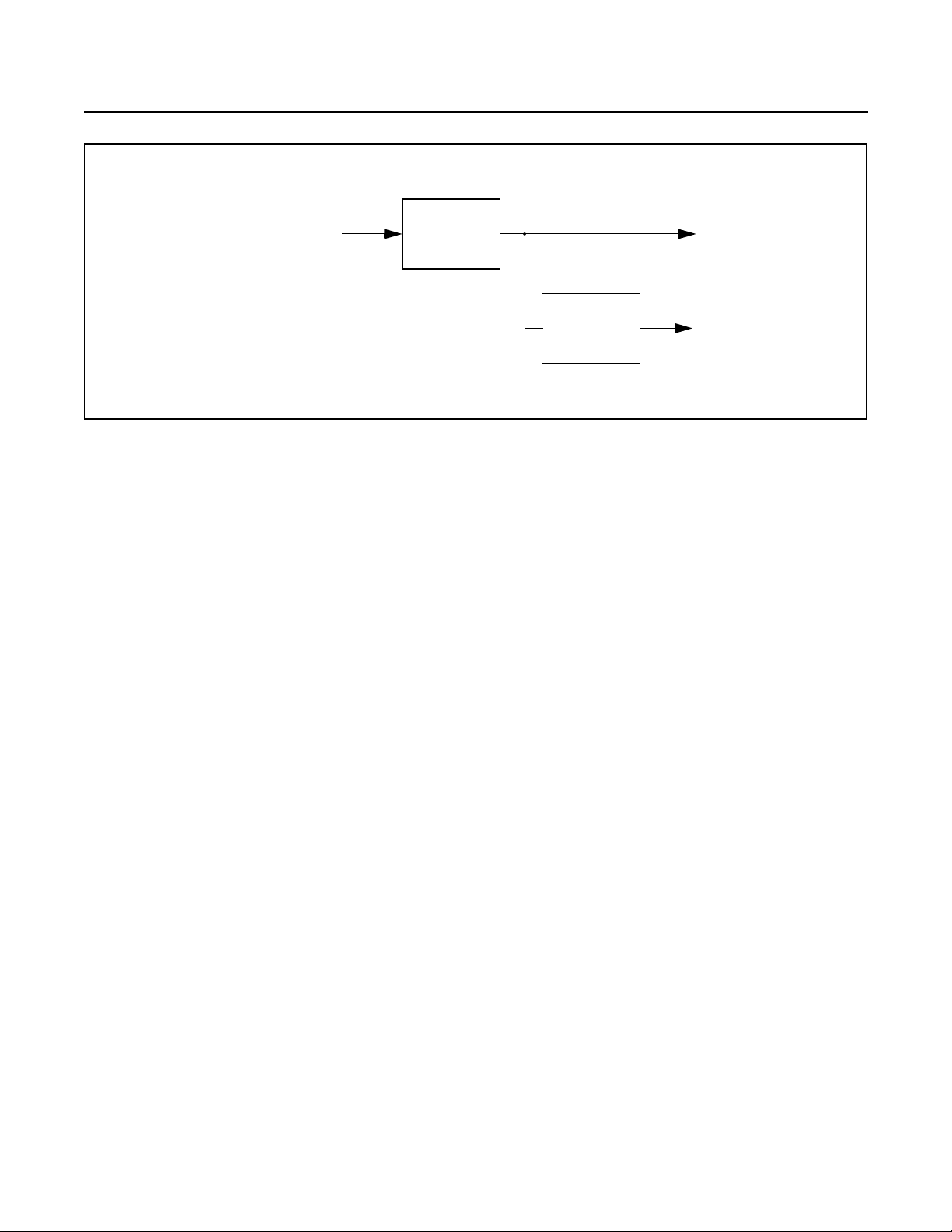
Philips Semiconductors Preliminary User Manual
LPC2119/2129/2292/2294ARM-based Microc ontroller
Crystal Oscillator
or
External Clock Source
)
(F
osc
PLL
Processor Clock
(cclk)
VPB Divider
Figure 16: VPB Divider Connections
VPB Clock
(pclk)
System Control Block 68 January 08, 2004
Page 69

Philips Semiconductors Preliminary User Manual
LPC2119/2129/2292/2294ARM-based Microc ontroller
WAKEUP TIMER
The purpose of the wakeup timer is to ensure that the oscillator and other analog functions required for chip operation are fully
functional before the pr ocessor is allowed to e xecute instructi ons. This is important at power on, all types of R eset, and whenever
any of the aforementioned functions are turned off for any reason. Since the oscillator and other functions are turned off during
Power Down mode, any wakeup of the processor from Power Down mode makes use of the Wakeup Timer.
The Wakeup Timer monitors the crystal oscillator as the means of checking whether it is safe to begin code execution. When
power is applied to the chip, or som e event ca used th e chip to exit Pow er down mode, som e time i s requir ed for the o scillato r to
produce a signal of su fficie nt amplitud e to dr ive the c lock logi c. The am ount of tim e depe nds on m any fac tors, inclu din g the rate
of Vdd ramp (in the cas e o f po w er on ), th e ty pe of c ry sta l a nd i ts ele ctri ca l characteristics (if a quartz c rys tal is us ed) , as well as
any other external circuit ry (e.g. cap acitor s), and the c haracte ristics of th e oscil lator its elf unde r the exis ting ambien t conditions.
Once a clock is detected, the Wakeup Timer counts 4096 clocks, then enables the Flash memory to initialize. When the Flash
memory initialization is complete, the processor is released to execute instructions if the external Reset has been de-asserted.
In the case where an external clock source is used in the system (as opposed to a crystal connected to the oscillator pins), the
possibility that there could be l ittle or no d elay for oscilla tor start-up m ust be consi dered. The Wake up Timer desi gn then ensures
that any other required chip functions will be operational prior to the beginning of program execution.
The LPC2119/2129/2292/2294 does not contain any analog function such as comparators that operate without clocks or any
independent clo ck source such as a dedica ted Watchdog o scillator. The on ly remaining functions that can operate i n the absence
of a clock source are the external interrupts (EINT0, EINT1, EINT2 and EINT3) and the CAN controllers. When an external
interrupt is enabled for wakrup, and its selected event occurs, an oscillator wakeup cycle is started. Similarly,if a CAN block is
enabled for wakeup and acti vity occ urs on it s CAN bus , an osci llator wak eup cycl e is sta trted. The a ctual int errupt (if an y) occurs
after the wakeup time expires, and is handled by the Vectored Interrupt Controller (VIC).
However, the pin mu ltiplexing on the LPC21 19/2129/2292/229 (see Pin Configuration on page 86 and Pin Conne ct Block on page
100) was designed to all ow oth er p erip hera ls to, i n ef fec t, bri ng the device out of power do wn m ode . The following pin-function
pairings allow interrupts from events relating to UAR T0 or 1, SPI 0 or 1, or the I
RxD1 / EINT3, DCD1 / EINT1, RI1 / EINT2, SSEL1 / EINT3.
To put the device in power down mode and allow activity on one or more of these buses or lines to power it back up, software
should reprogram the pi n function to Extern al Interrupt, sel ect the appropr iate mode and p olarity for the I nterrupt, and then select
power down mode. Upon wakeup software should restore the pin mulitplexing to the peripheral function.
All of the bus- or line-activity indications in the list above happen to be low-active. If software wants the device to come out of
power -down mode in response to actity on more than one pin that share the same EINTi channel, it should program low-level
sensitivity for that channel, because only in level mode will the channel logically OR the signals to wake the device.
The only flaw in this scheme is that th e time to resta rt the oscilla tor prevents the LPC2119/212 9/2292/229 fro m capturing the bus
or line activity th at wakes it up. Idle mode is more appropriate t han power-do wn mode for d evices that m ust capture and respond
to external activity in a timely manner.
To summarize: on the LPC2119/2129/2292/2294, the Wakeup Timer enforces a minimum reset duration based on the crystal
oscillator, and is activated whenever there is a wakeup from Power Down mode or any type of Reset.
2
C: RxD0 / EINT0, SDA / EINT1, SSEL0 / EINT2,
System Control Block 69 January 08, 2004
Page 70

Philips Semiconductors Preliminary User Manual
LPC2119/2129/2292/2294ARM-based Microc ontroller
5. MEMORY ACCELERATOR MODULE (MAM)
INTRODUCTION
Simply put, the Memory Accelerator Module (MAM) attempts to have the next ARM instruction that will be needed in its latches
in time to prevent CPU fetch stal ls. The me thod used is to split the Flash memory into two bank s , eac h cap abl e of ind ep end ent
accesses. Each of the two F lash bank s has its o wn Prefetc h Buffe r and Bra nch Tra il Buffe r. The Bra nch Tra il Buffe rs for t he two
banks capture two 128-b it l ine s of Fl as h da ta whe n an In struction Fetch is not satisfi ed b y ei ther the Prefetch buffer nor Branch
Trail buffer for its bank, and for which a prefetch has not been initiated. Each prefetch buffer captures one 128-bit line of
instructions from its Flash bank, at the conclusion of a prefetch cycle initiated speculatively by the MAM.
Each 128 bit value includes four 32-bit ARM instructions or eight 16-bit Thumb instructions. During sequential code execution,
typically one Flash bank contains or is fetching the current instruction and the entire Flash line that contains it. The other bank
contains or is prefetching the next sequential code line. After a code line delivers its last instruction, the bank that contained it
begins to fetch the next line in that bank.
Timing of Flash read operations is programmable and is described later in this section as well as in the System Control Block
section.
Branches and othe r pro gram f low c ha nges cause a break i n t he seq ue ntial flow of instructio n fe tches described above. When a
backward branch occurs, there is a distinct possibility that a loop is being executed. In this case the Branch Trail Buffers may
already contain the target instruction. If so, execution continues without the need for a Flash read cycle. For a forward branch,
there is also a chance that the new addres s is alre ady contai ned in one of the Pref etch Buff ers. If it is, t he branch is again taken
with no delay.
When a branch outsi de the c onten ts of the Branch Trail an d Prefetc h buffe rs is ta ken, one Fl ash Acces s cy cle is neede d to loa d
the Branch Trail buffers . Subseq uently , there w ill typic ally b e no furthe r fetch de lays until ano ther suc h “Instr uction Miss ” occurs.
The Flash memory controller detects data accesses to the Flash memory and uses a separate buffer to store the results in a
manner similar to that us ed during code fetches . This allows faster acces s to data if it is accessed sequ entially. A single li ne buffer
is provided for data accesses, as opposed to the two buffers per Flash bank that are provided for code accesses. There is no
prefetch function for data accesses.
Memory Accelerator Module Blocks
The Memory Accelerator Module is divided into several functional blocks:
• A Flash Address Latch for each bank. An Incrementer function is associated with the Bank 0 Flash Address latch.
• Two Flash Memory Banks.
• Instruction Latches, Data Latches, Address Comparison latches.
•Wait logic
Figure 17 shows a simplified block diagram of the Memory Accelerator Module data paths.
In the following de scription s, the term “fe tch” appl ies to an explicit Fl ash read request fro m the ARM. “ prefetch” i s used to denote
a Flash read of instructions beyond t he current p rocessor fetch address.
Flash Memory Banks
There are two banks of Flash memory in order to allow two parallel accesses and eliminate delays for sequential accesses.
Memory Accelerator Module (MAM) 70 January 08, 2004
Page 71
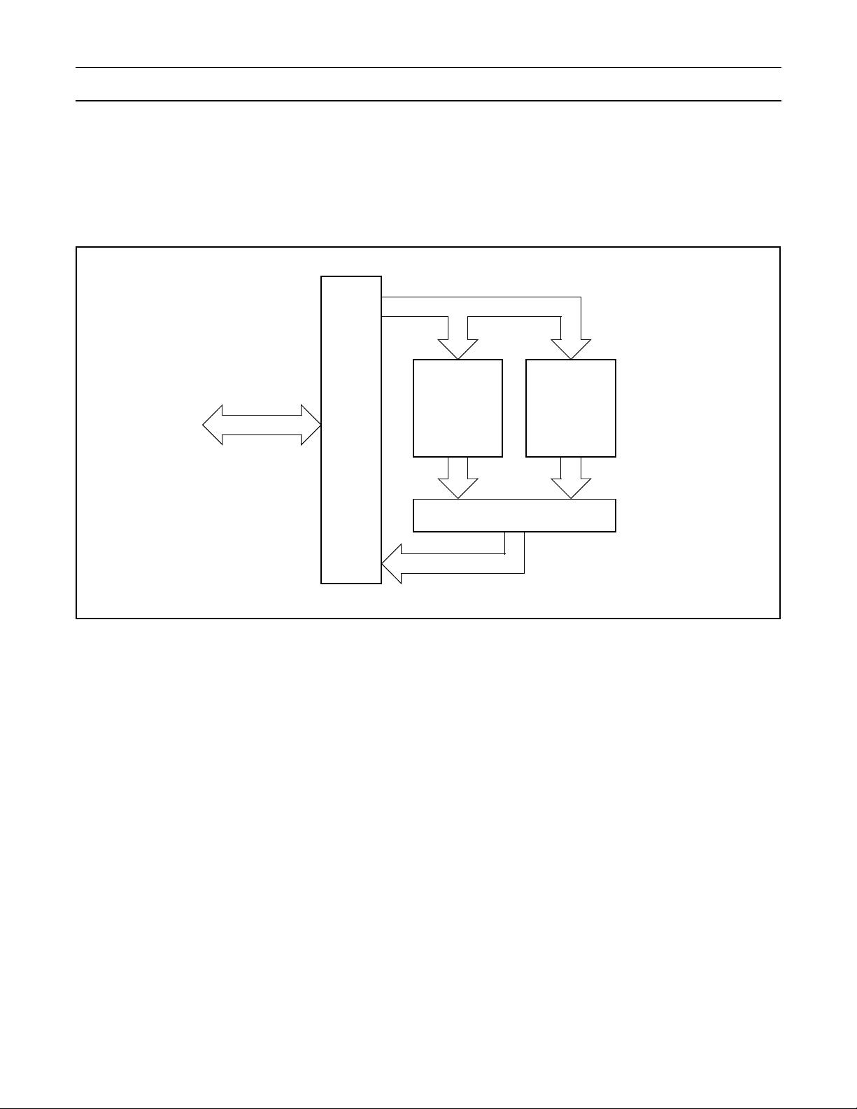
Philips Semiconductors Preliminary User Manual
LPC2119/2129/2292/2294ARM-based Microc ontroller
Flash programming oper ations are not con trolled by the Me mory Ac celera tor Modu le, but are handle d as a sep arate fun ction. A
“boot block” sector contains Flash programming algorithms that may be called as part of the application program, and a loader
that may be run to allow serial programming of the Flash memory.
The Flash memories are wired so that each sector exists in both banks, such that a sector erase operation acts on part of both
banks simultaneously. In effect, the existence of two banks is transparent to the programming functions.
Memory Address
Flash Memory
ARM Local Bus
Figure 17: Simplified Block Diagram of the Memory Accelerator Module
Bus
Interface
Bank 0
Selection
Memory Data
Flash Memory
Bank 1
Bank
Instruction Latches and Data Latches
Code and Data accesses are treated separately by the Memory Accelerator Module. There are two sets of 128-bit Instruction
Latches and 12 -bit Com parison Address Latc he s as soc ia t ed with each Flash Bank. One of the two se ts, ca ll ed the Branch Trail
Buffer, holds the data and comparison address for that bank from the last Instruction miss. The other set, called the Prefetch
Buffer, holds the data and comparison address from prefetches undertaken speculatively by the MAM. Each Instruction Latch
holds 4 words of code (4 ARM instructions, or 8 Thumb instructions).
Similarly there i s a 1 28-bit Data La tch and 1 3-bit Data Addr ess latch, tha t are u sed d uring D ata cycl es. This sing le se t of latches
is shared by bot h Flas h bank s. Eac h Data a cces s that is not in the Data latch caus es a F lash f etch o f 4 wo rds of data, wh ich ar e
captured in the Data latch. This speeds up sequential Data operations, but has little or no effect on random accesses.
Flash Programming Issues
Since the Flash memory does not al low accesses durin g programming and erase op erations, it is necessar y for the MAM to force
the CPU to wait if a memory access to a Flash address is requested while the Flash module is busy. (This is accomplished by
asserting the ARM7 TDMI-S local bu s signal CLKEN. ) Under some cond itions, this de lay could resu lt in a Watchdog time-out. The
user will need to be a ware of this pos sibilit y and take s teps to insu re that an unw anted Watc hdog reset d oes not cau se a system
failure while programming or erasing the Flash memory.
Memory Accelerator Module (MAM) 71 January 08, 2004
Page 72
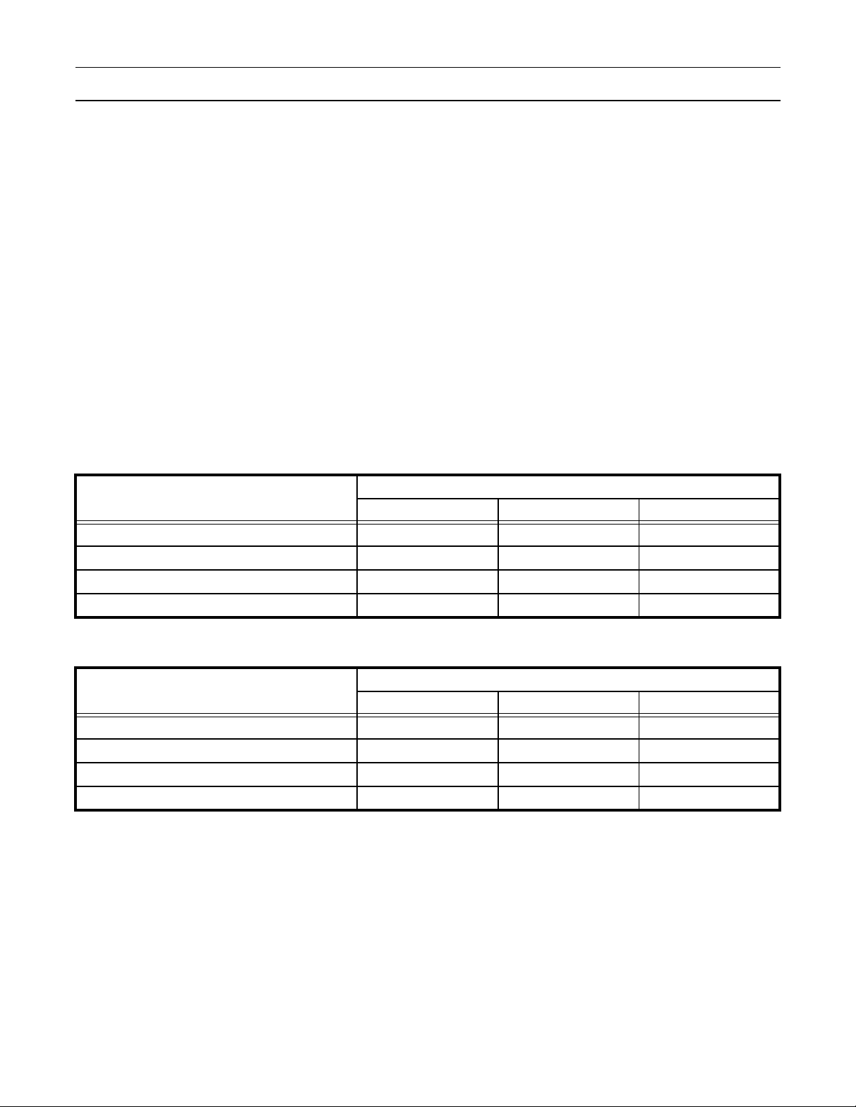
Philips Semiconductors Preliminary User Manual
LPC2119/2129/2292/2294ARM-based Microc ontroller
In order to preclude the possibility of stale data being read from the Flash memory, the MAM holding latches are automatically
invalidated at the be ginning of any Fl ash programming o r erase operation . Any subsequen t read from a Flash ad dress will cause
a new fetch to be initiated after the Flash operation has completed.
MEMORY ACCELERATOR MODULE OPERATING MODES
Three modes of operation are defined for the MAM, trading off performance for ease of predictability:
0) MAM off. All memory requests result in a Flash read operation (see note 2 below). There are no instruction prefetches.
1) MAM partially ena bl ed. Sequential instruc tion ac c ess es a re fulfilled from the ho ld ing latches if the data i s present. Instruction
prefetch is enabled. Non-sequential instruction accesses initiate Flash read operations (see note 2 below). This means that all
branches cause mem ory fe tches . All dat a opera tions c ause a Flash rea d b ecause bu ffe red data acce ss timin g is ha rd to pre dict
and is very situation dependent.
2) MAM fully enabled . Any memory request (code or data) for a value that is contai ned in one of the correspondi ng holding latches
is fulfilled from the latch. Instruction prefetch is enabled. Flash read operations are initiated for instruction prefetch and code or
data values not available in the corresponding holding latches.
Table 35: MAM Responses to Program Accesses of Various Types
Program Memory Request Type
MAM Mode
012
Sequential access, data in MAM latches Initiate Fetch
2
Use Latched Data
Sequential access, data not in MAM latches Initiate Fetch Initiate Fetch
Non-Sequential access, data in MAM latches Initiate Fetch
2
Initiate Fetch
Non-Sequential access, data not in MAM latches Initiate Fetch Initiate Fetch
1, 2
1
Use Latched Data
1
Initiate Fetch
Use Latched Data
1
Initiate Fetch
1
1
1
1
Table 36: MAM Responses to Data and DMA Accesses of Various Types
MAM Mode
Data Memory Request Type
012
Sequential access, data in MAM latches Initiate Fetch
2
Initiate Fetch
2
Use Latched Data
Sequential access, data not in MAM latches Initiate Fetch Initiate Fetch Initiate Fetch
Non-Sequential access, data in MAM latches Initiate Fetch
2
Initiate Fetch
2
Use Latched Data
Non-Sequential access, data not in MAM latches Initiate Fetch Initiate Fetch Initiate Fetch
1. Instruction prefetch is enabled in modes 1 and 2.
2. The MAM actually uses latch ed data if it i s availa ble, but mi mics the t iming of a F lash read o peratio n. This saves power whil e
resulting in the same execution timing. The MAM can truly be turned off by setting the fetch timing value in MAMTIM to one
clock.
Memory Accelerator Module (MAM) 72 January 08, 2004
Page 73

Philips Semiconductors Preliminary User Manual
LPC2119/2129/2292/2294ARM-based Microc ontroller
MAM CONFIGURATION
After reset the MAM defaults to the disabled state. Software can turn memory access acceleration on or off at any time. This
allows most of an application to be run at the highest possible performance, while certain functions can be run at a somewhat
slower but more predicta ble rate if more precise timing is requir ed.
REGISTER DESCRIPTION
All registers, regardless of size, are on word address boundaries. Details of the registers appear in the description of each
function.
Table 37: Summary of System Control Registers
Address Name Description Access
MAM
Memory Accelerator Module Control Register. Determines the MAM
0xE01FC000 MAMCR
0xE01FC004 MAMTIM
*Reset Value refers to the data stored in used bits only. It does not include reserved bits content.
functional mode, that is, to what extent the MAM performance
enhancements are enabled. See Table 38.
Memory Accelerator Module Timing control. Determines the number of
clocks used for Flash memory fetches (1 to 7 processor clocks).
Reset
Value*
R/W 0
R/W 0x07
Memory Accelerator Module (MAM) 73 January 08, 2004
Page 74

Philips Semiconductors Preliminary User Manual
LPC2119/2129/2292/2294ARM-based Microc ontroller
MAM Control Register (MAMCR - 0xE01FC000)
Two configuration bits select the three MAM operating modes, as shown in Table 38. Following Reset, MAM functions are
disabled. Changing the MAM operating mode causes the MAM to invalidate all of the holding latches, resulting in new reads of
Flash information as required.
Table 38: MAM Control Register (MAMCR - 0xE01FC000)
MAMCR Function Description
These bits determine the operating mode of the MAM as follows:
1:0
7:2 Reserved
MAM mode
control
0 0 - MAM functions disabled.
0 1 - MAM functions partially enabled.
1 0 - MAM functions fully enabled.
1 1 - reserved
Reserved, user software shou ld not write ones to reserved b its. The value rea d from a
reserved bit is not defined.
Reset
Value
0
NA
MAM Timing Register (MAMTIM - 0xE01FC004)
The MAM Timing regis ter determines how many cclk cycles are used to acces s the Flash memory. This al lows tuning MAM timing
to match the processor operating frequency. Flash access times from 1 clock to 7 clocks are possible. Single clock Flash
accesses would esse ntially remove the MAM fro m ti mi ng c alc ul atio ns . In this case the MAM mode may be se le cte d to optimize
power usage.
Table 39: MAM Timing Register (MAMTIM - 0xE01FC004)
MAMTIM Function Description
These bits set the duration of MAM Flash fetch operations as follows:
0 0 0 = 0 - Reserved.
0 0 1 = 1 - MAM fetch cycles are 1 processor clock (cclk) in duration.
0 1 0 = 2 - MAM fetch cycles are 2 processor clocks (cclks) in duration.
0 1 1 = 3 - MAM fetch cycles are 3 processor clocks (cclks) in duration.
1 0 0 = 4 - MAM fetch cycles are 4 processor clocks (cclks) in duration.
1 0 1 = 5 - MAM fetch cycles are 5 processor clocks (cclks) in duration.
1 1 0 = 6 - MAM fetch cycles are 6 processor clocks (cclks) in duration.
1 1 1 = 7 - MAM fetch cycles are 7 processor clocks (cclks) in duration.
2:0
MAM Fetch
Cycle timing
Reset
Value
0x07
Warning: Improper set tin g of t his v alue may result in inco rrect o perati on of the devi ce.
7:3 Reserved
Reserved, user software shou ld not write ones to reserved b its. The value rea d from a
reserved bit is not defined.
NA
MAM USAGE NOTES
When changing M AM timing, the MAM mu st f irs t be turn ed off by writing a ze ro t o M AMC R. A ne w value may then be w ritte n to
MAMTIM. Finally, the MAM may be turned on again by writing a value (1 or 2) corresponding to the desired operating mode to
MAMCR.
For system cloc k sl ower than 2 0 MH z, MA MTIM c an be 0 01. For s ystem clock betw een 20 M Hz and 40 M Hz , Flas h ac cess ti me
is suggested to be 2 CCLKs, while in systems with system clock faster than 40 MHz, 3 CCLKs are proposed.
Memory Accelerator Module (MAM) 74 January 08, 2004
Page 75

Philips Semiconductors Preliminary User Manual
LPC2119/2129/2292/2294ARM-based Microc ontroller
Memory Accelerator Module (MAM) 75 January 08, 2004
Page 76

Philips Semiconductors Preliminary User Manual
LPC2119/2129/2292/2294ARM-based Microc ontroller
6. VECTORED INTERRUPT CONTROLLER (VIC)
FEATURES
• ARM PrimeCell™ Vectored Interrupt Controller
• 32 interrupt request inputs
• 16 vectored IRQ interrupts
• 16 priority levels dynamically assigned to interrupt requests
• Software interrupt generation
DESCRIPTION
The Vectored Interrupt Con troller (VIC) takes 32 interrupt reque st inputs and p rogrammably assig ns them into 3 cate gories, FIQ,
vectored IRQ, and non-vectored IR Q. The program mable assig nment sche me means that priorities of interrupts from the v arious
peripherals can be dynamically assigned and adjusted.
Fast Interrupt reQuest (FIQ) requests have the highest priority. If more than one request is assigned to FIQ, the VIC ORs the
requests to produce the FIQ signal to the ARM processor. The fastest possible FIQ latency is achieved when only one request
is classified as FIQ, be caus e then the FIQ service rout ine can si mply start de aling with that de vice . But if m ore th an one requ est
is assigned to the FIQ class, the FIQ service routine can read a word from the VIC that identifies which FIQ source(s) is (are)
requesting an interrupt.
Vectored IRQs have the middle priority, but ony 16 of the 32 requests can be assig ne d to this category . Any of the 32 reques ts
can be assigned to any of the 16 vectored IRQ slots, among which slot 0 has the highest priority and slot 15 has the lowest.
Non-vectored IRQs have the lowest priority.
The VIC ORs the requests from all the vectored and non-vectored IRQs to produce the IRQ signal to the ARM processor. The
IRQ service routine can start by reading a register from the VIC and jumping there. If any of the vectored IRQs are requesting,
the VIC provides the address of the highe st-priority requesting IR Qs service routine, otherwis e it provides the address of a default
routine that is shared by al l the non-vectored IRQs. The default routine can read another VIC register to see what IRQs are active.
All registers in the VIC are word registers. Byte and halfword reads and write are not supported.
Additional information on the Vectored Interrupt Controller is available in the ARM PrimeCell™ Vectored Interrupt Controller
(PL190) documentation.
Vectored Interrupt Controller (VIC) 76 January 08, 2004
Page 77
Philips Semiconductors Preliminary User Manual
LPC2119/2129/2292/2294ARM-based Microc ontroller
REGISTER DESCRIPTION
The VIC implements the registers shown in Table 40. More detailed descriptions follow.
Table 40: VIC Register Map
Address Name Description Access
0xFFFF F000 VICIRQStatus
0xFFFF F004 VICFIQStatus
0xFFFF F008 VICRawIntr
0xFFFF F00C VICIntSelect
0xFFFF F010 VICIntEnable
0xFFFF F014 VICIntEnClr
0xFFFF F018 VICSoftInt
0xFFFF F01C VICSoftIntClear
0xFFFF F020 VICProtection
IRQ Status Register. This register reads out the state of those interrupt
requests that are enabled and classified as IRQ.
FIQ Status Requests. This register reads out the state of those interrupt
requests that are enabled and classified as FIQ.
Raw Interrupt Status Register. This register reads out the sta te of the 32
interrupt requests / software interrupts, regardless of enabling or
classification.
Interrupt Select Registe r. This regis ter classifi es each of the 32 interrupt
requests as contributing to FIQ or IRQ.
Interrupt Enable Register. This register controls which of the 32 interrupt
requests and software interrupts are enabled to contribute to FIQ or
IRQ.
Interrupt Enable Clear Register. This register allows software to clear
one or more bits in the Interrupt Enable register.
Software Interrupt Register . The co ntents of this register are ORed with
the 32 interrupt requests from various peripheral functions.
Software Interrupt Clear Regis ter. Thi s regis ter all ows sof tware to c lear
one or more bits in the Software Interrupt register.
Protection enable register. This registe r allows limiting access to the VIC
registers by software running in privileged mode.
Reset
Value*
RO 0
RO 0
RO 0
R/W 0
R/W 0
W0
R/W 0
W0
R/W 0
0xFFFF F030 VICVectAddr
0xFFFF F034 VICDefVectAddr
0xFFFF F100 VICVectAddr0
0xFFFF F104 VICVectAddr1 Vector address 1 register R/W 0
0xFFFF F108 VICVectAddr2 Vector address 2 register R/W 0
0xFFFF F10C VICVectAddr3 Vector address 3 register R/W 0
0xFFFF F110 VICVectAddr4 Vector address 4 register R/W 0
0xFFFF F114 VICVectAddr5 Vector address 5 register R/W 0
0xFFFF F118 VICVectAddr6 Vector address 6 register R/W 0
0xFFFF F11C VICVectAddr7 Vector address 7 register R/W 0
0xFFFF F120 VICVectAddr8 Vector address 8 register R/W 0
0xFFFF F124 VICVectAddr9 Vector address 9 register R/W 0
Vector Address Register. When an IRQ interrupt occurs, the IRQ service
routine can read this register and jump to the value read.
Default Vector Add res s Register. This regist er h ol ds the address of the
Interrupt Service routine (ISR) for non-vectored IRQs.
Vector address 0 register. Vector Address Registers 0-15 hold the
addresses of the Interrupt Service routines (ISRs) for the 16 vectored
IRQ slots.
R/W 0
R/W 0
R/W 0
Vectored Interrupt Controller (VIC) 77 January 08, 2004
Page 78

Philips Semiconductors Preliminary User Manual
LPC2119/2129/2292/2294ARM-based Microc ontroller
Table 40: VIC Register Map
Address Name Description Access
0xFFFF F128 VICVectAddr10 Vector address 10 register R/W 0
0xFFFF F12C VICVectAddr11 Vector address 11 register R/W 0
0xFFFF F130 VICVectAddr12 Vector address 12 register R/W 0
0xFFFF F134 VICVectAddr13 Vector address 13 register R/W 0
0xFFFF F138 VICVectAddr14 Vector address 14 register R/W 0
0xFFFF F13C VICVectAddr15 Vector address 15 register R/W 0
Vector control 0 re gister. Vector Control Registers 0-15 eac h control one
0xFFFF F200 VICVectCntl0
0xFFFF F204 VICVectCntl1 Vector control 1 register R/W 0
0xFFFF F208 VICVectCntl2 Vector control 2 register R/W 0
0xFFFF F20C VICVectCntl3 Vector control 3 register R/W 0
0xFFFF F210 VICVectCntl4 Vector control 4 register R/W 0
0xFFFF F214 VICVectCntl5 Vector control 5 register R/W 0
0xFFFF F218 VICVectCntl6 Vector control 6 register R/W 0
0xFFFF F21C VICVectCntl7 Vector control 7 register R/W 0
0xFFFF F220 VICVectCntl8 Vector control 8 register R/W 0
of the 16 vectored IRQ slots. Slot 0 has the highest priority and slot 15
the lowest.
R/W 0
Reset
Value*
0xFFFF F224 VICVectCntl9 Vector control 9 register R/W 0
0xFFFF F228 VICVectCntl10 Vector control 10 register R/W 0
0xFFFF F22C VICVectCntl11 Vector control 11 register R/W 0
0xFFFF F230 VICVectCntl12 Vector control 12 register R/W 0
0xFFFF F234 VICVectCntl13 Vector control 13 register R/W 0
0xFFFF F238 VICVectCntl14 Vector control 14 register R/W 0
0xFFFF F23C VICVectCntl15 Vector control 15 register R/W 0
*Reset Value refers to the data stored in used bits only. It does not include reserved bits content.
Vectored Interrupt Controller (VIC) 78 January 08, 2004
Page 79

Philips Semiconductors Preliminary User Manual
LPC2119/2129/2292/2294ARM-based Microc ontroller
VIC REGISTERS
This section describes the VIC registers in the order in which they are used in the VIC logic, from those closest to the interrupt
request inputs to tho se most abstracted for us e by software. For most p eople, this is also th e best order to read about the registers
when learning the VIC.
Software Interrupt Register (VICSoftInt - 0xFFFFF018, Read/Write)
The contents of this register are ORed with the 32 interrupt requests from the various peripherals, before any other logic is
applied.
Table 41: Software Interrupt Register (VICSoftInt - 0xFFFFF018, Read/Write)
VICSoftInt Function Reset Value
1:force the interrupt request with this bit number.
31:0
0: do not force the inte rrupt request w ith this bi t number. Writ ing zeroes to bits in VICS oftInt has
no effect, see VICSoftIntClear.
0
Software Interrupt Clear Register (VICSoftIntClear - 0xFFFFF01C, Write Only)
This register allows software to clear one or more bits in the Software Interrupt register, without having to first read it.
Table 42: Software Interrupt Clear Register (VICSoftIntClear - 0xFFFFF01C, Write Only)
VICSoftIntClear Function Reset Value
1: writing a 1 clears the corresponding bit in the Software Interrupt register, thus releasing
31:0
the forcing of this request.
0: writing a 0 leaves the corresponding bit in VICSoftInt unchanged.
0
Raw Interrupt Status Register (VICRawIntr - 0xFFFFF008, Read Only)
This register reads out the state of the 32 interrupt requests and software interrupts, regardless of enabling or classification.
Table 43: Raw Interrupt Status Register (VICRawIntr - 0xFFFFF008, Read-Only)
VICRawIntr Function Reset Value
31:0
1: the interrupt request or software interrupt with this bit number is asserted.
0: the interrupt request or software interrupt with this bit number is negated.
0
Vectored Interrupt Controller (VIC) 79 January 08, 2004
Page 80

Philips Semiconductors Preliminary User Manual
LPC2119/2129/2292/2294ARM-based Microc ontroller
Interrupt Enable Register (VICIntEnable - 0xFFFFF010, Read/Write)
This register controls which of the 32 interrupt requests and software interrupts contribute to FIQ or IRQ.
Table 44: Interrupt Enable Register (VICINtEnable - 0xFFFFF010, Read/Write)
VICIntEnable Function Reset Value
When this register is r ead, 1s indic ate in terrupt re quest s or so ftwar e interru pts th at are en abled
to contribute to FIQ or IRQ.
31:0
Interrupt Enable Clear Register (VICIntEnClear - 0xFFFFF014, Write Only)
This register allows software to clear one or more bits in the Interrupt Enable register, without having to first read it.
Table 45: Software Interrupt Clear Register (VICIntEnClear - 0xFFFFF014, Write Only)
When this register is written, on es enab le interru pt reque sts or sof tware interrupts to contri bute
to FIQ or IRQ, zeroes have no effe ct. See the VIC IntEnCle ar regis ter (Tab le 46 b elow ), for ho w
to disable interrupts.
0
VICIntEnClear Function Reset Valu e
1: writing a 1 clears the corresponding bit in the Interrupt Enable register, thus disabling
31:0
interrupts for this request.
0: writing a 0 leaves the corresponding bit in VICIntEnable unchanged.
0
Interrupt Select Register (VICIntSelect - 0xFFFFF00C, Read/Write)
This register classifies each of the 32 interrupt requests as contributing to FIQ or IRQ.
Table 46: Interrupt Select Register (VICIntSelect - 0xFFFFF00C, Read/Write)
VICIntSelect Function Reset Value
31:0
1: the interrupt request with this bit number is assigned to the FIQ category.
0: the interrupt request with this bit number is assigned to the IRQ category.
0
IRQ Status Register (VICIRQStatus - 0xFFFFF000, Read Only)
This register reads out the state of those interrupt requests that are enabled and classified as IRQ. It does not differentiate
between vectored and non-vectored IRQs.
Table 47: IRQ Status Register (VICIRQStatus - 0xFFFFF000, Read-Only)
VICIRQStatus Function Reset Value
31:0 1: the interrupt request with this bit number is enabled, cla ssifi ed as IRQ, and asserte d. 0
Vectored Interrupt Controller (VIC) 80 January 08, 2004
Page 81

Philips Semiconductors Preliminary User Manual
LPC2119/2129/2292/2294ARM-based Microc ontroller
FIQ Status Register (VICFIQStatus - 0xFFFFF004, Read Only)
This register reads out the state of those interrupt requests that are enabled and classified as FIQ. If more than one request is
classified as FIQ, the FIQ service routine can read this register to see which request(s) is (are) active.
Table 48: IRQ Status Register (VICFIQStatus - 0xFFFFF004, Read-Only)
VICFIQStatus Function Reset Value
31:0 1: the interrupt request with this bit number is enabled, cla ssifi ed as FIQ, and ass ert ed. 0
Vector Control Registers 0-15 (VICVectCntl0-15 - 0xFFFFF200-23C, Read/Write)
Each of these registers con trols one of the 16 vectored IRQ slots . Slot 0 has the hi ghest priori ty and slot 1 5 the lowest. N ote that
disabling a vectored IRQ slot in one of the VICVectCntl registers does not disable the interrupt itself, the interrupt is simply
changed to the non-vectored form.
Table 49: Vector Control Registers (VICVectCntl0-15 - 0xFFFFF200-23C, Read/Write)
VICVectCntl0-15 Function Reset Value
5
4:0
1: this vectored IRQ slot is enabled, and can produce a unique ISR address when its
assigned interrupt request or software interrupt is enabled, classified as IRQ, and asserted.
The number of the interrupt request or software interrupt assigned to this vectored IRQ slot.
As a matter of good programming practice, software should not assign the same interrupt
number to more than one enabled vectored IRQ slot. But if this does occur, the lowernumbered slot will be used when the interrupt request or software interrupt is enabled,
classified as IRQ, and asserted.
0
0
Vector Address Registers 0-15 (VICVectAddr0-15 - 0xFFFFF100-13 C, Read/Write)
These registers hold the addresses of the Interrupt Service routines (ISRs) for the 16 vectored IRQ slots.
Table 50: Vector Address Registers (VICVectAddr0-15 - 0xFFFFF100-13C, Read/Write)
VICVectAddr0-15 Function Reset Value
When one or more in terrupt req uest or s oftware int errupt is (are) enab led, class ified as IR Q,
31:0
asserted, and assign ed to a n e nabled vectored IRQ slot , th e v alu e from this register for the
highest-priority such slot will be provided when the IRQ service routine reads the Vector
Address register (VICVectAddr).
0
Default Vector Address Register (VICDefVectAddr - 0xFFFFF034, Read/Write)
This register holds the address of the Interrupt Service routine (ISR) for non-vectored IRQs.
Table 51: Default Vector Address Register (VICDefVectAddr - 0xFFFFF034, Read/Write)
VICDefVectAddr Function Reset Valu e
31:0
When an IRQ service routin e reads the Vec tor Address register (VIC VectAddr), and no IR Q
slot responds as described above, this address is returned.
0
Vectored Interrupt Controller (VIC) 81 January 08, 2004
Page 82

Philips Semiconductors Preliminary User Manual
LPC2119/2129/2292/2294ARM-based Microc ontroller
Vector Address Register (VICVectAddr - 0xFFFFF030, Read/Write)
When an IRQ interrupt occurs, the IRQ service routine can read this register and jump to the value read.
Table 52: Vector Address Register (VICVectAddr - 0xFFFFF030, Read/Write)
VICVectAddr Function Reset Value
If any of the inter rupt requests or software in terrupts that a re assigned to a vecto red IRQ slot
is (are) enabled, classified as IRQ, and asserted, reading from this register returns the
address in the Vector Addres s Regis ter for the highes t-priori ty such sl ot (low est-numb ered)
31:0
Protection Enable Register (VICProtection - 0xFFFFF020, Read/Write)
This one-bit register controls access to the VIC registers by software running in User mode.
such slot. Otherwise it returns the address in the Default Vector Address Register.
Writing to this register does not set the value for future reads from it. Rather, this register
should be written near the end of an ISR, to update the priority hardware.
0
Table 53: Protection Enable Register (VICProtection - 0xFFFFF020, Read/Write)
VICProtection Function Reset Value
0
1: the VIC registers can only be accessed in privileged mode.
0: VIC registers can be accessed in User or privileged mode.
0
Vectored Interrupt Controller (VIC) 82 January 08, 2004
Page 83

Philips Semiconductors Preliminary User Manual
LPC2119/2129/2292/2294ARM-based Microc ontroller
INTERRUPT SOURCES
Table 54 lists the interrupt sources for each peripheral function. Each peripheral device has one interrupt line connected to the
Vectored Interrupt Controller, but may have several internal interrupt flags. Individual interrupt flags may also represent more
than one interrupt source.
Table 54: Connection of Interrupt Sources to the Vectored Interrupt Controller
Block Flag(s) VIC Channel #
WDT Watchdog Interrupt (WDINT) 0
- Reserved for software interrupts only 1
ARM Core Embedded ICE, DbgCommRx 2
ARM Core Embedded ICE, DbgCommTx 3
TIMER0
TIMER1
Match 0 - 3 (MR0, MR1, MR2, MR3)
Capture 0 - 3 (CR0, CR1, CR2, CR3)
Match 0 - 3 (MR0, MR1, MR2, MR3)
Capture 0 - 3 (CR0, CR1, CR2, CR3)
Rx Line Status (RLS)
UART0
Transmit Holding Register Empty (THRE)
Rx Data Available (RDA)
Character Time-out Indicator (CTI)
Rx Line Status (RLS)
Transmit Holding Register Empty (THRE)
UART1
Rx Data Available (RDA)
Character Time-out Indicator (CTI)
Modem Status Interrupt (MSI)
PWM0
2
C SI (state change) 9
I
SPI0
SPI1
Match 0 - 6 (MR0, MR1, MR2, MR3, MR4, MR5, MR6)
Capture 0 - 3 (CR0, CR1, CR2, CR3)
SPI Interrupt Flag (SPIF)
Mode Fault (MODF)
SPI Interrupt Flag (SPIF)
Mode Fault (MODF)
PLL PLL Lock (PLOCK) 12
RTC
Counter Increment (RTCCIF)
Alarm (RTCALF)
4
5
6
7
8
10
11
13
System Control External Interrupt 0 (EINT0) 14
System Control External Interrupt 1 (EINT1) 15
System Control External Interrupt 2 (EINT2) 16
System Control External Interrupt 2 (EINT2) 17
A/D A/D Converter 18
CAN and Acceptance Filter
CAN
1 ORed CAN, LUTerr int
2x(Tx int, Rx int) LPC2119/2129/2292/2294
2x(Tx int, Rx int) LPC2294 only
19
20-23
24-27
Vectored Interrupt Controller (VIC) 83 January 08, 2004
Page 84
Philips Semiconductors Preliminary User Manual
LPC2119/2129/2292/2294ARM-based Microc ontroller
nVICFIQIN
VICINT
SOURCE
[31:0]
Interrupt Request, Masking, and Selection
SoftIntClear
[31:0]
SoftInt
[31:0]
RawInterrupt
[31:0]
Vector Interrupt 0
Source Enable
VectorCntl[5:0]
Vector Interrupt 1 Priority 1
IntEnableClear
[31:0]
IntEnable
[31:0]
IntSelect
[31:0]
Priority 0
VectorAddr
Priority 2
[31:0]
FIQStatus
[31:0]
IRQStatus
[31:0]
VectIRQ0
VectAddr0[31:0]
VectIRQ1
VectAddr1[31:0]
Non-vectored FIQ Interrupt Logic
FIQStatus
[31:0]
Non-vectored IRQ Interrupt Logic
Priority
Logic
IRQ
IRQ
Address Select for
Highest Priority
Interrupt
IRQStatus
[31:0]
Interrupt Priority Logic
Hardware
NonVectIRQ
VectorAddr
[31:0]
nVICFIQ
nVICIRQ
VICVECT
ADDROUT
[31:0]
Vector Interrupt 15 Priority 14
Priority 15
VectIRQ15
VectAddr15[31:0]
VICVECTADDRIN[31:0]nVICIRQIN
Default
VectorAddr
[31:0]
Figure 18: Block Diagram of the Vectored Interrupt Controller
Vectored Interrupt Controller (VIC) 84 January 08, 2004
Page 85

Philips Semiconductors Preliminary User Manual
LPC2119/2129/2292/2294ARM-based Microc ontroller
VIC USAGE NOTES
If user’s code is runing from the on-chip RAM and an aplication uses interrupts, interrupt vectors must be re-mapped to flash
address 0x0. This is nece ssary because all the except ion vectors are located at addre sses 0x0 and above. This is easily achieved
by configuring MEMM AP registe r (locat ed in Sys tem Con trol Bloc k) to User R AM mod e. App licat ion co de shou ld be li nked s uch
that at 0x4000 0000 the Interrupt Vector Tabe (IVT) will reside.
Although multiple sources can be selected (VICIntSelect) to generate FIQ request, only one interrupt service routine should be
dedicated to service al l avail able/p resent FIQ reque st(s). Th erefore, i f more than one inte rrupt sou rces are classifi ed as FIQ the
FIQ interrupt service rout ine must read VICFIQSta tus to decide based on thi s content what to do and how to process the interrupt
request. However, it is recommended that only one interrupt source should be classified as FIQ. Classifying more than one
interrupt sources as FIQ will increase the interrupt latency.
Following the compl etion of the desired interrupt service routine, clea ring of the interrupt flag on the peripheral level will propagate
to corresponding bits in VIC registers (VICRawIntr, VICFIQStatus and VICIRQStatus). Also, before the next interrupt can be
serviced, it is necessary that write is performed into the VICVectAddr register before the return from interrupt is executed. This
write will clear the respective interrupt flag in the internal interrupt priority hardware.
In order to disable the interrupt at the VIC you need to clear corresponding bit in the VICIntEnClr register, which in turn clears
the related bit in the VICIntEnable registe r. This also applies to the VICSo ftIn t a nd VICSoftIntClear in which VI CSoftIn tClear will
clear the respective bits in VICSoftInt. For example, if VICSoftInt=0x0000 0005 and bit 0 has to be cleared,
VICSoftIntClear=0x0000 0001 will acom plish this. Be fore the new cl ear operatio n on the sam e bit in VICSof tInt using writin g into
VICSoftIntClear is performed in the future, VICSoftIntClear= 0x0000 0000 must be assi gned. Therefore writing 1 to any bit in Clear
register will have one-time-effect in the destination register.
If the watchdog is enable d for interru pt on unde rflow or in vali d feed seq uence only then there is no way of c learing the interrupt.
The only way you could perform return from interrupt is by disabling the interrupt at the VIC(using VICIntEnClr).
Example:
Assuming that UART0 and SPI0 are generating interrupt requests that are classified as vectored IRQs (UART0 being on the
higher level than SPI0), while UART1 and I
setup:
VICIntSelect = 0x0000 0000(SPI0, I2C, UART1 and UART0 are IRQ => bit10, bit9, bit7 and bit6=0)
VICIntEnable = 0x0000 06C0(SPI0, I2C, UART1 and UART0 are enabled interrupts => bit10, bit9, bit 7 and bit6=1)
VICDefVectAddr = 0x… (holds address at what routine for servicing non-vectored IRQs (i.e. UART1 and I2C) starts)
VICVectAddr0 = 0x… (holds address where UART0 IRQ service routine starts)
VICVectAddr1 = 0x… (holds address where SPI0 IRQ service routine starts)
VICVectCntl0 = 0x0000 0026(interrupt source with index 6 (UART0) is enabled as the one with priority 0 (the highest))
VICVectCntl1 = 0x0000 002A(interrupt source with index 10 (SPI0) is enabled as the one with priority 1)
After any of IRQ requests (SPI0, I2C, UART0 or UART1) is made, microcontroller will redirect code execution to the address
specified at location 0x00000018. For vectored and non-vectored IRQ’s the following instruction could be placed at 0x18:
LDR pc,[pc,#-0xFF0]
This instruction loads PC with the address that is present in VICVectAddr register.
In case UART0 request has been made, VICVectAddr will be identical to VICVectAddr0, while in case SPI0 request has been
made value from VICVectAddr1 will be found here. If neither UART0 nor SPI0 have generated IRQ request but UART1 and/or
2
I
C were the reason, content of VICVectAddr will be identical to VICDefVectAddr.
2
C are generating non-vectored IRQs, the following could be one possibility for VIC
Vectored Interrupt Controller (VIC) 85 January 08, 2004
Page 86
Philips Semiconductors Preliminary User Manual
LPC2119/2129/2292/2294ARM-based Microc ontroller
7. PIN CONFIGURATION
LPC2119/2129 PINOUT
P0.21/PWM5/CAP1.3
P0.22/CAP0.0/MAT0.0
P0.23/RD2
P1.19/TRACEPKT3
P0.24/TD2
V
SS
V
P1.18/TRACEPKT2
P0.25/RD1
TD1
P0.27/AIN0/CAP0.1/MAT0.1
P1.17/TRACEPKT1
P0.28/AIN1/CAP0.2/MAT0.2
P0.29/AIN2/CAP0.3/MAT0.3
P0.30/AIN3/EINT3/CAP0.0
P1.16/TRACEPKT0
18A
P1.27 / TD0
V
XTAL1
XTAL2
64
63
62
61
1
2
3
4
5
6
7
3A
8
9
10
11
12
13
14
15
16
SSA
P1.28 / TDI
60
SSA_PLL
V
V
RESET
P1.29 / TCK
P0.20 / MAT1.3 / SSEL1 / EINT3
P0.19 / MAT1.2 / MOSI1 / CAP1.2
P0.18 / CAP1.3 / MISO1 / MAT1.3
P1.30 / TMS
59
58
57
56
55
54
53
52
3
V
51
SS
18
P
V
50
49
48
P1.20/TRACESYNC
P0.17/CAP1.2 /SCK1/MAT1.2
47
P0.16/EINT0/MAT0.2/CAP0.2
46
P0.15/RI1/EINT2
45
P1.21/PIPESTAT0
44
V
43
3
V
42
41
40
39
38
37
36
35
34
33
SS
P0.14/DCD1/EINT1
P1.22/PIPESTAT1
P0.13/DTR1/MAT1.1
P0.12/DSR1/MAT1.0
P0.11/CTS1/CAP1.1
P1.23/PIPESTAT2
P0.10/RTS1/CAP1.0
P0.9/RxD1/PWM6/EINT3
P0.8/TxD1/PWM4
17
18
19
20
21
22
23
24
25
26
27
28
29
30
31
32
18
SS
V
V
P1.3 / TRST
P0.0 / TxD0 / PWM1
P0.1 / RxD0 / PWM3 / EINT0
3
V
P0.2 / SCL / CAP0.0
P1.26 / RTCK
SS
V
P1.25 / EXTIN0
P0.4 / SCK0 / CAP0.1
P0.3 / SDA / MAT0.0 / EINT1
P0.6 / MOSI0 / CAP0.2
P0.5 / MISO0 / MAT0.1
P1.24 / TRACECLK
P0.7 / SSEL0 / PWM2/ EINT2
Figure 19: LPC2119/2129 64-pin package
Pin Configuration 86 January 08, 2004
Page 87

Philips Semiconductors Preliminary User Manual
LPC2119/2129/2292/2294ARM-based Microc ontroller
PIN DESCRIPTION FOR LPC2119/2129
Pin description for LPC2119/2129 and a brief of corresponding functions are shown in the following table.
Table 55: Pin description for LPC2119/2129
Pin
Name
P0.0
to
P0.31
LQFP64
Pin #
19
21
22
26
27
29
Type Description
Port 0: Port 0 is a 32-bit bi-directional I/O port with individual direction controls for each bit. The
I/O
operation of port 0 pins depends upon the pin function selected via the Pin Connect Block.
Pins 26 and 31 of port 0 are not available.
O
O
O
I/O
I/O
O
I/O
I/O
O
P0.0 TxD0 Transmitter output for UART0.
PWM1 Pulse Width Modulator out put 1.
I
P0.1 RxD0 Receiver input for UART0.
PWM3 Pulse Width Modulator out put 3.
I
P0.2 SCL I
I
P0.3 SDA I
P0.4 SCK0 Serial Clock for SPI0. SPI clock output from master or input to slave.
I
P0.5 MISO0 Master In Slave Out for SPI0. Data input to SPI master or data output
EINT0 External interrupt 0 input.
2
C clock input/output. Open drain output (for I2C compliance).
CAP0.0 Capture input for TIMER0, channel 0.
2
C data input/output. Open drain output (for I2C compliance).
MAT0.0 Match output for TIMER0, channel 0.
EINT1 External interrupt 1 input.
CAP0.1 Capture input for TIMER0, channel 1.
from SPI slave.
MAT0.1 Match output for TIMER0, channel 1.
30
31
33
34
35
37
I/O
O
O
O
O
O
P0.6 MOSI0 Master Out Slave In for SPI0. Data output from SPI master or data
input to SPI slave.
I
I
P0.7 SSEL0 Slave Select for SPI0. Selects the SPI interface as a slave.
I
P0.8 TxD1 Transmitter output for UART1.
I
P0.9 RxD1 Receiver input for UART1.
I
P0.10 RTS1 Request to Send output for UART1.
I
I
P0.11 CTS1 Clear to Send input for UART1.
I
CAP0.2 Capture input for TIMER0, channel 2.
PWM2 Pulse Width Modulator out put 2.
EINT2 External interrupt 2 input.
PWM4 Pulse Width Modulator out put 4.
PWM6 Pulse Width Modulator out put 6.
EINT3 External interrupt 3 input.
CAP1.0 Capture input for TIMER1, channel 0.
CAP1.1 Capture input for TIMER1, channel 1.
Pin Configuration 87 January 08, 2004
Page 88

Philips Semiconductors Preliminary User Manual
LPC2119/2129/2292/2294ARM-based Microc ontroller
Table 55: Pin description for LPC2119/2129
Pin
Name
LQFP64
Pin #
38
39
41
45
46
47
53
Type Description
I
P0.12 DSR1 Data Set Ready input for UART1.
O
O
O
O
I/O
O
I/O
O
P0.13 DTR1 Data Terminal Ready output for UART1.
I
P0.14 DCD1 Data Carrier Detect input for UART1.
I
I
P0.15 RI1 Ring Indicator input for UART1.
I
I
P0.16 EINT0 External interrupt 0 input.
I
I
P0.17 CAP1.2 Capture input for TIMER1, channel 2.
I
P0.18 CAP1.3 Capture input for TIMER1, channel 3.
MAT1.0 Match output for TIMER1, channel 0.
MAT1.1 Match output for TIMER1, channel 1.
EINT1 External interrupt 1 input. LOW on this pine while RESET
forces on-chip boot-loader to take over control of the part after reset.
EINT2 External interrupt 2 input.
MAT0.2 Match output for TIMER0, channel 2.
CAP0.2 Capture input for TIMER0, channel 2.
SCK1 Serial Clock for SPI1. SPI clock output from master or input to slave.
MAT1.2 Match output for TIMER1, channel 2.
MISO1 Master In Slave Out for SPI1. Data input to SPI master or data output
from SPI slave.
MAT1.3 Match output for TIMER1, channel 3.
is LOW
O
54
55
1
2
3I
5O
9I
11
I/O
O
O
I
I
O
I
I
O
I
I
O
P0.19 MAT1.2 Match output for TIMER1, channel 2.
MOSI1 Master Out Slave In for SPI1. Data output from SPI master or data
input to SPI slave.
CAP1.2 Capture input for TIMER1, channel 2.
P0.20 MAT1.3 Match output for TIMER1, channel 3.
SSEL1 Slave Select for SPI1. Selects the SPI interface as a slave.
EINT3 External interrupt 3 input.
P0.21 PWM5 Pulse Width Modulator out put 5.
CAP1.3 Capture input for TIMER1, channel 3.
P0.22 CAP0.0 Capture input for TIMER0, channel 0.
MAT0.0 Match output for TIMER0, channel 0.
P0.23 RD2 CAN2 receiver input.
P0.24 TD2 CAN2 tran smitter output.
P0.25 RD1 CAN1 receiver input.
P0.27 AIN0 A/D converter, input 0. This analog input is always connected to its pin.
CAP0.1 Capture input for TIMER0, channel 1.
MAT0.1 Match output for TIMER0, channel 1.
Pin Configuration 88 January 08, 2004
Page 89
Philips Semiconductors Preliminary User Manual
LPC2119/2129/2292/2294ARM-based Microc ontroller
Table 55: Pin description for LPC2119/2129
Pin
Name
P1.16
to
P1.31
LQFP64
Pin #
13
14
15
16 O
12 O
Type Description
I/O
8O
4O
I
P0.28 AIN1 A/D converter, input 1. This analog input is always connected to its pin.
I
O
I
P0.29 AIN2 A/D converter, input 2. This analog input is always connected to its pin.
I
O
I
P0.30 AIN3 A/D converter, input 3. This analog input is always connected to its pin.
I
I
Port 1: Port 1 is a 32-bit bi-directional I/O port with individual direction controls for each bit. The
operation of port 1 pins depends upon the pin function selected via the Pin Connect Block.
Only pins 16 through 31 of port 1 are available.
P1.16 TRACEPKT0Trace Packet, bit 0. Standard I/O port with internal pull-up.
P1.17 TRACEPKT1Trace Packet, bit 1. Standard I/O port with internal pull-up.
P1.18 TRACEPKT2Trace Packet, bit 2. Standard I/O port with internal pull-up.
P1.19 TRACEPKT3Trace Packet, bit 3. Standard I/O port with internal pull-up.
CAP0.2 Capture input for TIMER0, channel 2.
MAT0.2 Match output for TIMER0, channel 2.
CAP0.3 Capture input for TIMER0, channel 3.
MAT0.3 Match output for TIMER0, channel 3.
EINT3 External interrupt 3 input.
CAP0.0 Capture input for TIMER0, channel 0.
48 O
44 O
40 O
36 O
32 O
28 I
I/O
24
64 O
60 I
P1.20 TRACESYNCTrace Synchroniz ation. Standard I/O port with internal pull-up. LOW on
this pin while RESET is LOW enables pins P1.25:16 to operate as a
Trace port after reset.
P1.21 PIPESTAT0 Pipeline Status, bit 0. St a ndard I/O port with internal pull-up.
P1.22 PIPESTAT1 Pipeline Status, bit 1. St a ndard I/O port with internal pull-up.
P1.23 PIPESTAT2 Pipeline Status, bit 2. St a ndard I/O port with internal pull-up.
P1.24 TRACECLK Trace Clock. Standard I/O port with internal pull-up.
P1.25 EXTIN0 External Trigger Input. Standard I/O with internal pull-up.
P1.26 RTCK Returned Test Clock output. Extra signal added to the JTAG port.
Assists debugger synchronization when processor frequency varies.
Bi-directional pin with internal pullup. LOW on thispin while RESET
LOW enables pins P1.31:26 to operate as a Debug port after reset.
P1.27 TDO Test Data out for JTAG interface.
P1.28 TDI Test Data in for JTAG interface.
is
Pin Configuration 89 January 08, 2004
Page 90
Philips Semiconductors Preliminary User Manual
LPC2119/2129/2292/2294ARM-based Microc ontroller
Table 55: Pin description for LPC2119/2129
Pin
Name
TD1 10 O
LQFP64
Pin #
56 I
52 I
20 I
Type Description
P1.29 TCK Test Clock for JTAG interface.
P1.30 TMS Test Mode Select for JTAG interface.
P1.31 TRST
Test Reset for JTAG interface.
TD1:CAN1 transmitter output.
External Reset input: A LOW on t his pi n resets the devic e, cau sing I/ O ports and per ipheral s to
RESET
57 I
take on their default sta tes , and proc es so r exe cu tio n to be gi n at ad dres s 0. TTL wi th hy st eres is ,
5V tolerant.
XTAL1 62 I Input to the oscillator circuit and internal clock generator circuits.
XTAL2 61 O Output from the oscillator amplifier.
SS
18
18A
3
3A
6, 18, 25,
42, 50
59 I
58 I
I Ground: 0V reference.
Analog Ground: 0V reference. Thi s should nom inally be the sam e voltage as V
isolated to minimize noise and error.
PLL Analog Ground: 0V reference. This should nominally be the same voltage as V
should be isolated to minimize noise and error.
17, 49 I 1.8V Core Power Supply: This is the power supply voltage for internal circuitry.
63 I
23, 43,
51
7I
Analog 1.8V Core Power Supply: This is the power supply voltage for internal circuitry. This
should be nominall y the sa me vol tage as V18 but sh ould be isola ted to mi nimiz e nois e and error .
I 3.3V Pad Power Supply: This is the power supply voltage for the I/O ports.
Analog 3.3V Pad Power Supply: This should be nominally the same voltage as V3 but should
be isolated to minimize noise and error.
V
V
SSA
V
SSA_PLL
V
V
V
V
but should be
SS,
but
SS,
Pin Configuration 90 January 08, 2004
Page 91
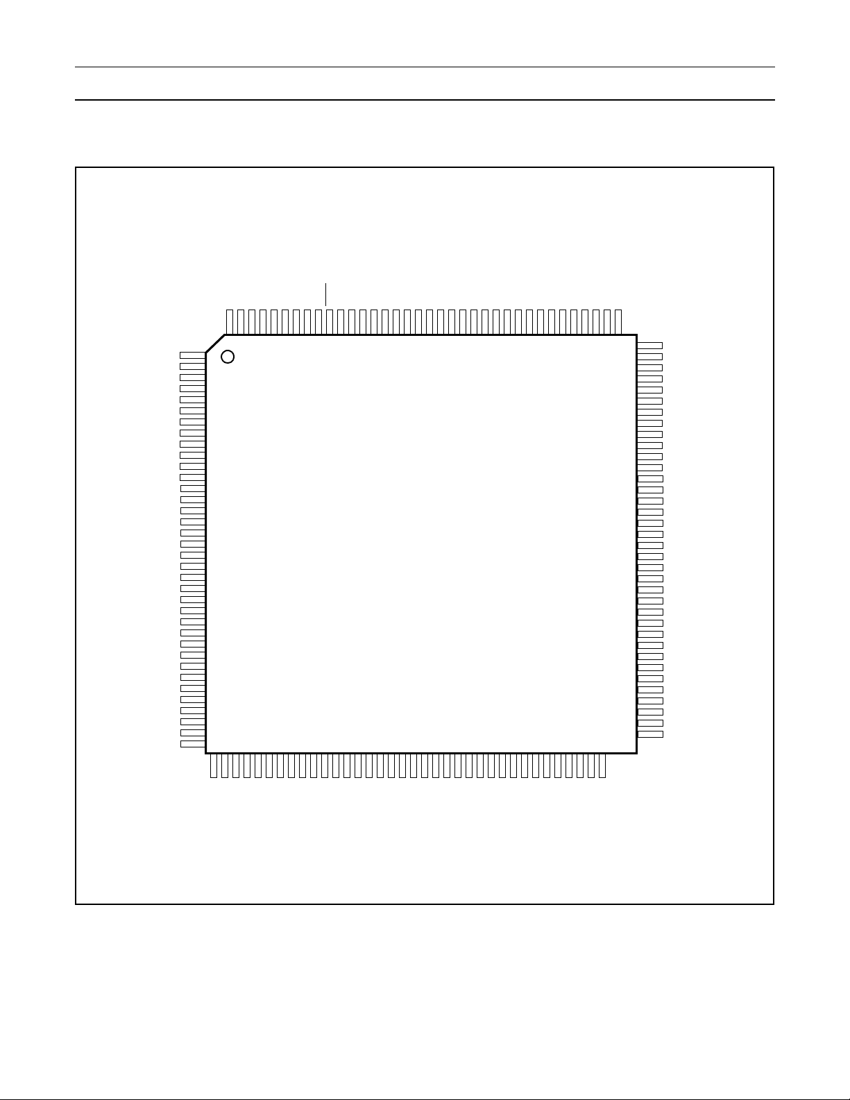
Philips Semiconductors Preliminary User Manual
LPC2119/2129/2292/2294ARM-based Microc ontroller
LPC2292/2294 PINOUT
P1.27/TDO
V18A
XTAL1
XTAL2
P1.28/TDI
VSSA
VSSA_PLL
P2.21/D21
P2.20/D20
RESET
P2.19/D19
P2.18/D18
P2.17/D17
P2.16/D16
P2.15/D15
P2.14/D14
VSS
P2.13/D13
P1.29/TCK
P2.12/D12
P2.11/D11
P0.20/MAT1.3/SSEL1/EINT3 P0.19/MAT1.2/MOSI1/CAP1.2
P0.18/CAP1.3/MISO1/MAT1.3
P2.10/D10
V3
P2.9/D9
P2.8/D8
P2.7/D7
P2.6/D6
P2.5/D5
P1.30/TMS
V3
VSS
V18
P2.4/D4
144
143
142
141
140
139
138
137
136
135
134
133
132
131
130
129
128
127
126
125
124
123
122
121
120
119
118
117
116
115
114
113
112
111
110
109
P2.3/D3
VSS
P2.2/D2
P2.1/D1
V3
VSS
P1.20/TRACESYNC
P0.17/CAP1.2/SCK1/MAT1.2
P0.16/EINT0/MAT0.2/CAP0.2
P0.15/RI1/EINT2
P2.0/D0
P3.30/BLS1
P3.31/BLS0
P1.21/PIPESTAT0
V3
VSS
P0.14/DCD1/EINT1
P1.0/CS0
P1.1/OE
P3.0/A0
P3.1/A1
P3.2/A2
P1.22/PIPESTAT1
P0.13/DTR1/MAT1.1/TD4
P0.12/DSR1/MAT1.0/RD4
P0.11/CTS1/CAP1.1
P1.23/PIPESTAT2
P3.3/A3
P3.4/A4
VSS
P0.10/RTS1/CAP1.0
V3
P0.9/RxD1/PWM6/EINT3
P0.8/TxD1/PWM4
P3.5/A5
P3.6/A6
1
1
VSS
VSS
V3A
TD1
VSS
1
2
V3
3
4
5
6
7
8
9
10
11
12
13
14
15
16
17
18
19
20
21
22
23
24
25
26
27
28
29
30
31
V3
32
33
34
35
36
37
38
39
40
V3
V18
VSS
P3.23/A23/XCLK
P2.22/D22
P0.21/PWM5/RD3
P0.22/TD3
P0.27/AIN0/CAP0.1/MAT0.1
P0.28/AIN1/CAP0.2/MAT0.2
P0.29/AIN2/CAP0.3/MAT0.3
P0.30/AIN3/EINT3/CAP0.0
1
CAN3 and CAN4 are available in LPC2294 only
1
/CAP1.3
1
/CAP0.0/MAT0.0
P0.23/RD2
P1.19/TRACEPKT3
P0.24/TD2
P2.23/D23
P2.24/D24
P2.25/D25
P2.26/D26/BOOT0
P1.18/TRACEPKT2
P2.27/D27/BOOT1
P2.28/D28
P2.29/D29
P2.30/D30/AIN4
P2.31/D31/AIN5
P0.25/RD1
P1.17/TRACEPKT1
P3.29/BLS2/AIN6
P3.28/BLS3/AIN7
P3.27/WE
P3.26/CS1
P1.16/TRACEPKT0
P3.25/CS2
P3.24/CS3
108
107
106
105
104
103
102
101
100
99
98
97
96
95
94
93
92
91
90
89
88
87
86
85
84
83
82
81
80
79
78
77
76
75
74
73
41
42
43
44
45
46
47
48
49
50
51
52
53
54
55
56
57
58
59
60
61
62
63
64
65
66
67
68
69
70
71
72
V3
P3.22/A22
P3.21/A21
P3.20/A20
P3.19/A19
P3.18/A18
P1.31 / TRST
P0.0 / TxD0 / PWM1
P3.17/A17
P0.1 / RxD0 / PWM3 / EINT0
P3.16/A16
P1.26 / RTCK
P0.2 / SCL / CAP0.0
V3
VSS
P3.15/A15
P3.14/A14
P0.3 / SDA / MAT0.0 / EINT1
P3.13/A13
P3.12/A12
P1.25 / EXTIN0
P0.4 / SCK0 / CAP0.1
P0.5 / MISO0 / MAT0.1
Vss
P3.9/A9
P3.11/A11
P3.10/A10
P3.8/A8
P3.7/A7
P1.24 / TRACECLK
P0.6 / MOSI0 / CAP0.2
P0.7 / SSEL0 / PWM2/ EINT2
Figure 20: LPC2292/2294 144-pin package
Pin Configuration 91 January 08, 2004
Page 92

Philips Semiconductors Preliminary User Manual
LPC2119/2129/2292/2294ARM-based Microc ontroller
PIN DESCRIPTION FOR LPC2292/2294
Pin description for LPC2292/2294 and a brief of corresponding functions are shown in the following table.Pin Description
Table 56: Pin description for LPC2292/2294
Pin
Name
P0.0
to
P0.31
LQFP144
Pin #
42,49,50,58,59
,61,68,69,75,7
6,78,83-
85,92,99,100,1
01,121-123,4-
6,8,21,23,25,3
2,33
42 O
49
50 I/O
58 I/O
59 I/O
Type Description
Port 0: Port 0 is a 32-bit bi-direction al I/O port with individu al direction con trols for each bit.
I/O
The operation of port 0 pins depends upon the pin function selected via the Pin Connect
Block.
Pins 26 and 31 of port 0 are not available.
P0.0 TxD0 Transmitter output for UART0.
O
I
P0.1 RxD0 Receiver input for UART0.
O
I
P0.2 SCL I
I
P0.3 SDA I
O
I
P0.4 SCK0 Serial Clock for SPI0. SPI clock output from master or input to
I
PWM1 Pulse Width Modulator output 1.
PWM3 Pulse Width Modulator output 3.
EINT0 External interrupt 0 input.
2
C clock input/output. Open drain out put (for I2C compliance).
CAP0.0 Capture input for TIMER0, channel 0.
2
C data input/output. Open drain output (for I2C compliance).
MAT0.0 Match output for TIMER0, channel 0.
EINT1 External interrupt 1 input.
slave.
CAP0.1 Capture input for TIMER0, channel 1.
61 I/O
O
68 I/O
69 I
O
75
76 I
O
O
O
P0.5 MISO0 Master In Slave Out for SPI0. Data input to SPI master or data
output from SPI slave.
MAT0.1 Match output for TIMER0, channel 1.
P0.6 MOSI0 Master Out Slave In for SPI0. Data output from SPI master or
data input to SPI slave.
I
P0.7 SSEL0 Slave Select for SPI0. Selects the SPI interface as a slave.
I
P0.8 TxD1 Transmitter output for UART1.
P0.9 RxD1 Receiver input for UART1.
I
CAP0.2 Capture input for TIMER0, channel 2.
PWM2 Pulse Width Modulator output 2.
EINT2 External interrupt 2 input.
PWM4 Pulse Width Modulator output 4.
PWM6 Pulse Width Modulator output 6.
EINT3 External interrupt 3 input.
Pin Configuration 92 January 08, 2004
Page 93

Philips Semiconductors Preliminary User Manual
LPC2119/2129/2292/2294ARM-based Microc ontroller
Table 56: Pin description for LPC2292/2294
Pin
Name
LQFP144
Pin #
78
83
84
85
92 I
99 I
100 I
Type Description
O
O
O
O
O
O
P0.10 RTS1 Request to Send output for UART1.
I
I
P0.11 CTS1 Clear to Send input for UART1.
I
I
P0.12 DSR1 Data Set Ready input for UART1.
I
P0.13 DTR1 Data Terminal Ready output for UART1.
P0.14 DCD1 Data Carrier Detect input for UART1.
I
P0.15 RI1 Ring Indicator input for UART1.
I
P0.16 EINT0 External interrupt 0 input.
I
CAP1.0 Capture input for TIMER1, channel 0.
CAP1.1 Capture input for TIMER1, channel 1.
MAT1.0 Match output for TIMER1, channel 0.
RD4 CAN4 receiver input (available in LPC2294 only).
MAT1.1 Match output for TIMER1, channel 1.
TD4 CAN4 transmitter output (available in LPC2294 only).
EINT1 External interrupt 1 input. LOW on this pin while RESET
forces on-chip boot-loader to take over control of the part after
reset.
EINT2 External interrupt 2 input.
MAT0.2 Match output for TIMER0, channel 2.
CAP0.2 Capture input for TIMER0, channel 2.
is LOW
101 I
I/O
121 I
I/O
122 O
I/O
123 O
4
P0.17 CAP1.2 Capture input for TIMER1, channel 2.
SCK1 Serial Clock for SPI1. SPI clock output from master or input to
slave.
O
P0.18 CAP1.3 Capture input for TIMER1, channel 3.
O
P0.19 MAT1.2 Match output for TIMER1, channel 2.
O
P0.20 MAT1.3 Match output for TIMER1, channel 3.
I
I
O
P0.21 PWM5 Pulse Width Modulator output 5.
I
I
MAT1.2 Match output for TIMER1, channel 2.
MISO1 Master In Slave Out for SPI1. Data input to SPI master or data
output from SPI slave.
MAT1.3 Match output for TIMER1, channel 3.
MOSI1 Master Out Slave In for SPI1. Data output from SPI master or
data input to SPI slave.
CAP1.2 Capture input for TIMER1, channel 2.
SSEL1 Slave Select for SPI1. Selects the SPI interface as a slave.
EINT3 External interrupt 3 input.
RD3 CAN3 receiver input (available in LPC2294 only).
CAP1.3 Capture input for TIMER1, channel 3.
Pin Configuration 93 January 08, 2004
Page 94

Philips Semiconductors Preliminary User Manual
LPC2119/2129/2292/2294ARM-based Microc ontroller
Table 56: Pin description for LPC2292/2294
Pin
Name
LQFP144
Pin #
5
6I
8O
21 I
23 I
25 I
32 I
Type Description
O
I
O
I
O
I
O
I
O
P0.22 TD3 CAN3 transmitter output (available in LPC2294 only).
CAP0.0 Capture input for TIMER0, channel 0.
MAT0.0 Match output for TIMER0, channel 0.
P0.23 RD2 CAN2 receiver input.
P0.24 TD2 CAN2 transmitter output.
P0.25 RD1 CAN1 receiver input.
P0.27 AIN0 A/D converter, input 0. This analog input is always connected to
its pin.
CAP0.1 Capture input for TIMER0, channel 1.
MAT0.1 Match output for TIMER0, channel 1.
P0.28 AIN1 A/D converter, input 1. This analog input is always connected to
its pin.
CAP0.2 Capture input for TIMER0, channel 2.
MAT0.2 Match output for TIMER0, channel 2.
P0.29 AIN2 A/D converter, input 2. This analog input is always connected to
its pin.
CAP0.3 Capture input for TIMER0, channel 3.
MAT0.3 Match output for TIMER0, channel 3.
P1.0
to
P1.31
33 I
91,90,34,24,15
,7,102,95,86,8
2,70,60,52,144
,140,126,113,
43
91 O
90 O
34 O
24 O
15 O
7O
P0.30 AIN3 A/D converter, input 3. This analog input is always connected to
its pin.
I
I
Port 1: Port 1 is a 32-bit bi-direction al I/O port with individu al direction con trols for each bit.
I/O
The operation of port 1 pins depends upon the pin function selected via the Pin Connect
Block.
Pins 2 through 15 of port 1 are not available.
P1.0 CS0 Low-active Chip Select 0 signal.
P1.1 OE Low -active Output Enable signal.
P1.16 TRACEPKT0Trace Packet, bit 0. Standard I/O port with internal pull-up.
P1.17 TRACEPKT1Trace Packet, bit 1. Standard I/O port with internal pull-up.
P1.18 TRACEPKT2Trace Packet, bit 2. Standard I/O port with internal pull-up.
P1.19 TRACEPKT3Trace Packet, bit 3. Standard I/O port with internal pull-up.
EINT3 External interrupt 3 input.
CAP0.0 Capture input for TIMER0, channel 0.
(Bank 0 addresses range 8000 0000 - 80FF FFFF)
Pin Configuration 94 January 08, 2004
Page 95
Philips Semiconductors Preliminary User Manual
LPC2119/2129/2292/2294ARM-based Microc ontroller
Table 56: Pin description for LPC2292/2294
Pin
Name
LQFP144
Pin #
102 O
95 O
86 O
82 O
70 O
60 I
52 I/O
144 O
Type Description
P1.20 TRACESYNCTrace Synchronization. Standard I/O port with internal pull-up.
LOW on this pin while RESET
operate as a Trace port after reset.
P1.21 PIPESTAT0 Pipeline Status, bit 0. Standard I/O port with internal pull-up.
P1.22 PIPESTAT1 Pipeline Status, bit 1. Standard I/O port with internal pull-up.
P1.23 PIPESTAT2 Pipeline Status, bit 2. Standard I/O port with internal pull-up.
P1.24 TRACECLK Trace Clock. Standard I/O port with internal pull-up.
P1.25 EXTIN0 External Trigger Input. Standard I/O with internal pull-up.
P1.26 RTCK Returned Test Clock output. Extra signal added to the JTAG
port. Assists debugger synchronization when processor
frequency varies. Bi-directional pin with internal pullup. LOW on
this pin while RESET
as a Debug port after reset.
P1.27 TDO Test Data out for JTAG interface.
is LOW enables pins P1.31:26 to operate
is LOW enables pins P1.25:16 to
P2.0
to
P2.31
140 I
126 I
113 I
43 I
98,105,106,10
8,109,114-
118,120,124,1
25,127,129-
134,136,137,1,
10-13,16-20
98 I/O
105 I/O
106 I/O
108 I/O
109 I/O
P1.28 TDI Test Data in for JTAG interface.
P1.29 TCK Test Clock for JTAG interface.
P1.30 TMS Test Mode Select for JTAG interface.
P1.31 TRST
Port 2: Port 2 is a 32-bit bi-direction al I/O port with individu al direction con trols for each bit.
I/O
The operation of port 2 pins depends upon the pin function selected via the Pin Connect
Block.
P2.0 D0 External memory data line 0.
P2.1 D1 External memory data line 1.
P2.2 D2 External memory data line 2.
P2.3 D3 External memory data line 3.
P2.4 D4 External memory data line 4.
Test Reset for JTAG interface.
Pin Configuration 95 January 08, 2004
Page 96

Philips Semiconductors Preliminary User Manual
LPC2119/2129/2292/2294ARM-based Microc ontroller
Table 56: Pin description for LPC2292/2294
Pin
Name
LQFP144
Pin #
114 I/O
115 I/O
116 I/O
117 I/O
118 I/O
120 I/O
124 I/O
125 I/O
127 I/O
129 I/O
130 I/O
Type Description
P2.5 D5 External memory data line 5.
P2.6 D6 External memory data line 6.
P2.7 D7 External memory data line 7.
P2.8 D8 External memory data line 8.
P2.9 D9 External memory data line 9.
P2.10 D10 External memor y data line 10.
P2.11 D11 External memory data line 11.
P2.12 D12 External memor y data line 12.
P2.13 D13 External memor y data line 13.
P2.14 D14 External memor y data line 14.
P2.15 D15 External memor y data line 15.
131 I/O
132 I/O
133 I/O
134 I/O
136 I/O
137 I/O
1I/O
10 I/O
11 I/O
12 I/O
P2.16 D16 External memor y data line 16.
P2.17 D17 External memor y data line 17.
P2.18 D18 External memor y data line 18.
P2.19 D19 External memor y data line 19.
P2.20 D20 External memor y data line 20.
P2.21 D21 External memor y data line 21.
P2.22 D22 External memor y data line 22.
P2.23 D23 External memor y data line 23.
P2.24 D24 External memor y data line 24.
P2.25 D25 External memor y data line 25.
Pin Configuration 96 January 08, 2004
Page 97

Philips Semiconductors Preliminary User Manual
LPC2119/2129/2292/2294ARM-based Microc ontroller
Table 56: Pin description for LPC2292/2294
Pin
Name
LQFP144
Pin #
13 I/O
16 I/O
17 I/O
18 I/O
19 I/O
Type Description
P2.26 D26 External memor y data line 26.
I
P2.27 D27 External memor y data line 27.
I
P2.28 D28 External memor y data line 28.
P2.29 D29 External memor y data line 29.
P2.30 D30 External memor y data line 30.
I
BOOT0 While RESET is low, together with BOOT1 controls booting and
internal operation. Internal pullup ensures high state if pin is left
unconnected.
BOOT1 While RESET is low, together with BOOT0 controls booting and
internal operation. Internal pullup ensures high state if pin is left
unconnected.
BOOT1:0=00 selects 8-bit memory on CS0 for boot.
BOOT1:0=01 selects 16-bit memory on CS0 for boot.
BOOT1:0=10 selects 32-bit memory on CS0 for boot.
BOOT1:0=11 selects Internal Flas h memory.
AIN4 A/D converter, input 4. This analog input is always connected to
its pin.
P3.0
to
P3.31
20 I/O
89-
87,81,80,74-
71,66-
62,56,55,53,48
-
44,41,40,36,35
,30-27,97,96
89 O
88 O
87 O
81 O
80 O
74 O
73 O
P2.31 D31 External memor y data line 31.
I
Port 3: Port 3 is a 32-bit bi-direction al I/O port with individu al direction con trols for each bit.
I/O
The operation of port 3 pins depends upon the pin function selected via the Pin Connect
Block.
P3.0 A0 External memory address line 0.
P3.1 A1 External memory address line 1.
P3.2 A2 External memory address line 2.
P3.3 A3 External memory address line 3.
P3.4 A4 External memory address line 4.
P3.5 A5 External memory address line 5.
P3.6 A6 External memory address line 6.
AIN5 A/D converter, input 5. This analog input is always connected to
its pin.
Pin Configuration 97 January 08, 2004
Page 98

Philips Semiconductors Preliminary User Manual
LPC2119/2129/2292/2294ARM-based Microc ontroller
Table 56: Pin description for LPC2292/2294
Pin
Name
LQFP144
Pin #
72 O
71 O
66 O
65 O
64 O
63 O
62 O
56 O
55 O
53 O
48 O
Type Description
P3.7 A7 External memory address line 7.
P3.8 A8 External memory address line 8.
P3.9 A9 External memory address line 9.
P3.10 A10 External memory address line 10.
P3.11 A11 External memory address line 11.
P3.12 A12 External memory address line 12.
P3.13 A13 External memory address line 13.
P3.14 A14 External memory address line 14.
P3.15 A15 External memory address line 15.
P3.16 A16 External memory address line 16.
P3.17 A17 External memory address line 17.
47 O
46 O
45 O
44 O
41 O
40 I/O
O
36
35
30 O
29 O
O P3.24 CS3 Low-active Chip Select 3 signal.
O P3.25 CS2 Low-active Chip Select 2 signal.
P3.18 A18 External memory address line 18.
P3.19 A19 External memory address line 19.
P3.20 A20 External memory address line 20.
P3.21 A21 External memory address line 21.
P3.22 A22 External memory address line 22.
P3.23 A23 External memory address line 23.
XCLK Clock output.
(Bank 3 addresses range 8300 0000 - 83FF FFFF)
(Bank 2 addresses range 8200 0000 - 82FF FFFF)
P3.26 CS1 Low-active Chip Select 1 signal.
(Bank 1 addresses range 8100 0000 - 81FF FFFF)
P3.27 WE Low-active Write enable signal.
Pin Configuration 98 January 08, 2004
Page 99

Philips Semiconductors Preliminary User Manual
LPC2119/2129/2292/2294ARM-based Microc ontroller
Table 56: Pin description for LPC2292/2294
Pin
Name
LQFP144
Pin #
28 O
Type Description
P3.28 BLS3 Low-active Byte Lane Select signal (Bank 3).
I
AIN7 A/D converter, input 7. This analog input is always connected to
its pin.
27 O
P3.29 BLS2 Low-active Byte Lane Select signal (Bank 2).
I
AIN6 A/D converter, input 6. This analog input is always connected to
its pin.
97 O
96 O
TD1 22 O
P3.30 BLS1 Low-active Byte Lane Select signal (Bank 1).
P3.31 BLS0 Low-active Byte Lane Select signal (Bank 0).
TD1:CAN1 transmitter output.
External Reset input: A LOW on this pin resets the device, causing I/O ports and
RESET
135 I
peripherals to take on their default st ates , and proce ss or ex ec utio n to beg in at add res s 0.
TTL with hysteresis, 5V tolerant.
XTAL1 142 I Input to the oscillator circuit and internal clock generator circuits.
XTAL2 141 O Output from the oscillator amplifier.
3, 9, 26, 38, 54,
SS
67, 79, 93, 103,
V
I Ground: 0V reference.
107, 111, 128
V
SSA
V
ssA_PLL
139 I
138 I
Analog Ground: 0V reference. This should nominally be the same voltage as V
should be isolated to minimize noise and error.
PLL Analog Ground: 0V reference. This should nominally be the same voltage as V
should be isolated to minimize noise and error.
V18 37, 110 I 1.8V Core Power Supply: This is the power supply voltage for internal circuitry.
Analog 1.8V Core Power Supply: This is the power supply voltage for internal circuitry.
V18A 143 I
This should be nominal ly the same voltage as V18 bu t should be isolated to m inimize noise
and error.
2, 31, 39, 51,
V3
57, 77, 94, 104,
I 3.3V Pad Power Supply: This is the power supply voltage for the I/O ports.
112, 119
V3A 14 I
Analog 3.3V Pad Power Supply: This should be nominally the same voltage as V3 but
should be isolated to minimize noise and error.
SS,
but
SS,
but
Pin Configuration 99 January 08, 2004
Page 100
Philips Semiconductors Preliminary User Manual
LPC2119/2129/2292/2294ARM-based Microc ontroller
8. PIN CONNECT BLOCK
FEATURES
• Allows individual pin configuration
APPLICATIONS
The purpose of the Pin Connect Block is to configure the microcontroller pins to the desired functions.
DESCRIPTION
The pin connect blo ck allows sele cted pi ns of the mi crocontroller to have more than one fu nction. Con figuration register s control
the multiplexers to allow connection between the pin and the on chip peripherals.
Peripherals should be connected to the appropriate pins prior to being activated, and prior to any related interrupt(s) being
enabled. Activity of any enabled peripheral function that is not mapped to a related pin should be considered undefined.
REGISTER DESCRIPTION
The Pin Control Module contains 2 registers as shown in Table 57. below.
Table 57: Pin Connect Block Register Map
Address Name Description Access
0xE002C000 PINSEL0 Pin function select register 0 Read/Write
0xE002C004 PINSEL1 Pin function select register 1 Read/Write
0xE002C014 PINSEL2 Pin function select register 2 Read/Write
Pin Connect Block 100 January 08, 2004
 Loading...