

Page 1

Colour Television Module
SHARP LCD 2k8
LK315D3LZ43, -LZ73
LK315T3LA33
LK315T3LZ53, -LZ93,
LQ315T3LZ23
LK370D3LZ33, -LZ43
LK370T3LZ53
LK520D3LZ13, -LZ33, -LZ83, -LZ93, -LZ9P
Contents Page
1. Technical Specifications, Connections, and Chassis
Overview 2
2. Safety Instructions, Warnings, and Notes 6
3. Directions for Use 7
4. Mechanical Instructions 8
5. Service Modes, Error Codes, and Fault Finding 30
6. Block Diagrams, Test Point Overviews, and
Waveforms 53
7. Circuit Diagrams and PWB Layouts 53
8. Alignments 53
9. Circuit Descriptions, Abbreviation List, and IC Data
Sheets 53
10. Spare Parts List 53
11. Revision List 53
©
Copyright 2008 Koninklijke Philips Electronics N.V.
All rights reserved. No part of this publication may be reproduced, stored in a
retrieval system or transmitted, in any form or by any means, electronic,
mechanical, photocopying, or otherwise without the prior permission of Philips.
Published by MW 0872 BU TV Consumer Care Printed in the Netherlands Subject to modification EN 3122 785 17812
Page 2
EN 2 LCD SHARP 2k81.
Technical Specifications, Connections, and Chassis Overview
1. Technical Specifications, Connections, and Chassis Overview
Index of this chapter:
1.1 Introduction
1.2 General
1.3 Specifications
Note:
• Specifications are indicative (subject to change).
1.1 Introduction
In this Service Manual you will find all necessary information to
perform the Board Level Repair (= board swap) scenario on
LCD panels. These LCD repair manuals are created per brand,
and they will contain all necessary information for the different
panels used in Philips flat LCD TVs.
1.2 General
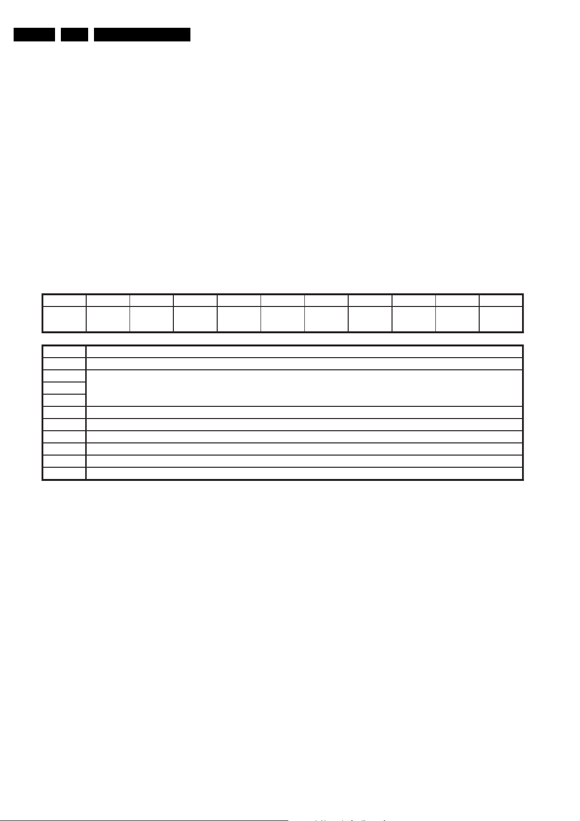
1234567891011
LK5 20D3LZ3 3
1
Display technology: L= LCD
2
Production plant: K= Kameyama plant (AVC)
3
\
4
> Screensize: 520= 52-inch
5
/
6
Display resolution: D= Full HD, T= WXGA (16:9)
7
Display type: 3= Transmissive type for standard AV usage.
8
Input signal type: A= Analogue RGB, C= Composite, L= LVDS
9
Z= Internal Sharp
10
See pt. 11
11 33= serial no, internal use and the second digit 3 indicate that this panel is for Philips
1.3 Specifications
Below find attached the data sheets of the different LCD
panels. Click on the “model number” to open.
• LK315D3LZ43
• LK315D3LZ73
• LK315T3LA33
• LK315T3LZ53
• LK315T3LZ93
• LQ315T3LZ23
• LK370D3LZ33
• LK370D3LZ43
• LK370T3LZ53
• LK520D3LZ13
• LK520D3LZ33
• LK520D3LZ83
• LK520D3LZ93
• LK520D3LZ9P
Figure 1-1 Nomenclature explanation (example)
I_18810_012.eps
290808
Page 3
Technical Specifications, Connections, and Chassis Overview
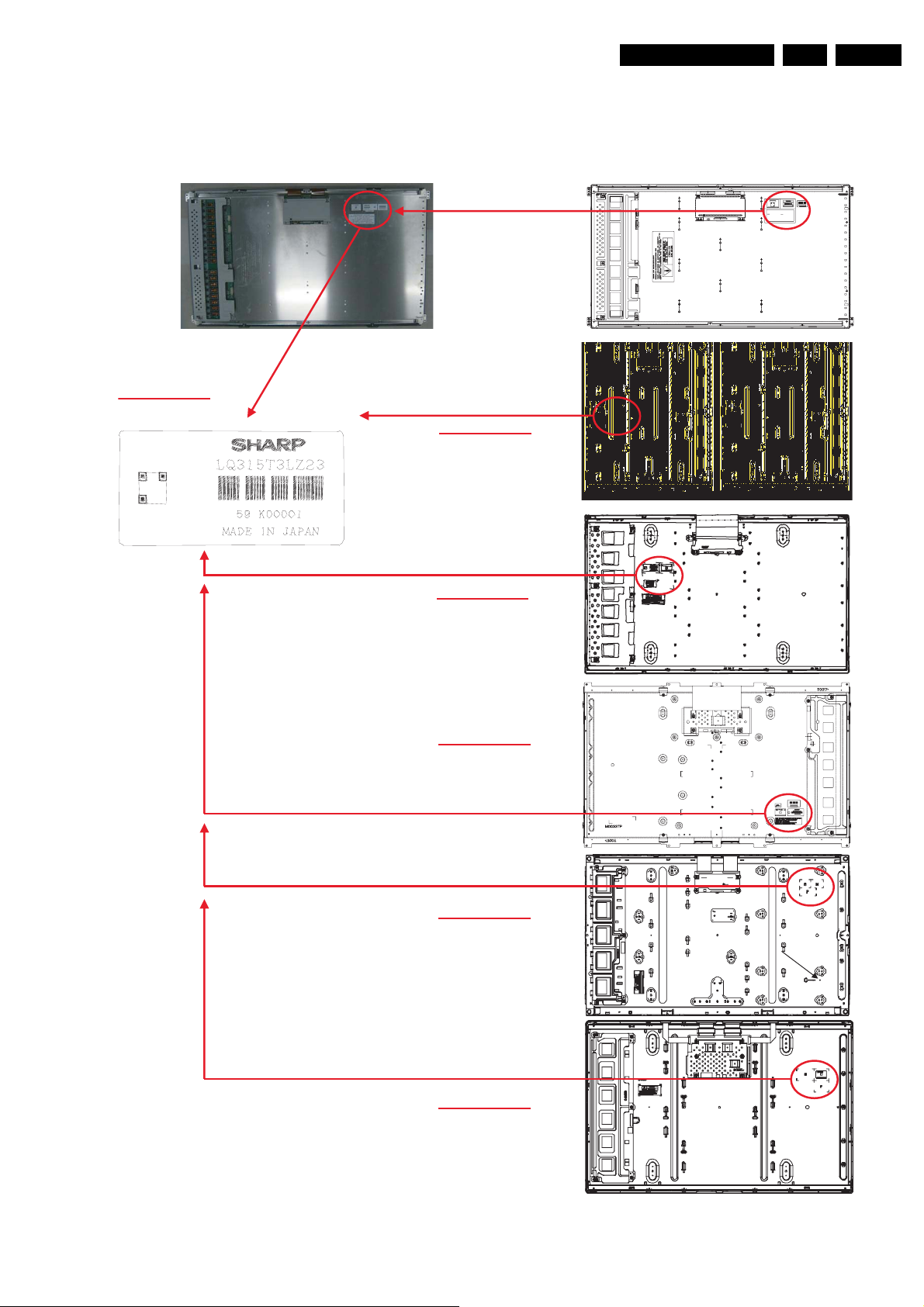
1.4 Board and Label Locations
1.4.1 32-inch models
LQ315T3LZ23
LQ315T3LZ23
Bar-code label
LK315D3LZ93
(Bar-code label
Is same as this
t
ype of Label)
EN 3LCD SHARP 2k8 1.
䌍䌁䌔䌅䌒䌉䌁䌌䇭䌉䌎䌆䌏䌒䌍䌁䌔䌉䌏䌎
䌏䌐䌔䌉䌃䌁䌌䇭䌆䌉䌌䌍 䋺䋾䌐䌃䋬䌐 䌅䌓䌔䋬䌁䌋䌕䌒䋭 䌘䋬䌐䌃䋼
䌄䌉䌆䌆䌕䌓䌅䌒䇭䌓䌈䌅䌅䌔䋺䋾䌐䌅 䌔䋼
䌄䌉䌆䌆䌕䌓䌅䌒䇭䌂䌏䌁䌒䌄䋺䋾䌍䌍䌁䋯䌓䋼
䌒䌅䌆䌌䌅䌃䌔䌏䌒䋺䋾䌐䌅䌔䋼
LK315T3LZ53
(Bar-code label
Is same as this
type of Label)
LK315D3LZ43
(Bar-code label
Is same as this
type of Label)
LK315T3LA33
(Bar-code label
Is same as this
type of Label)
LK315D3LZ73
(Bar-code label
Is same as this
type of Label)
Figure 1-2 Board and label location (32-inch models)
I_17812_001.eps
051208
Page 4
EN 4 LCD SHARP 2k81.
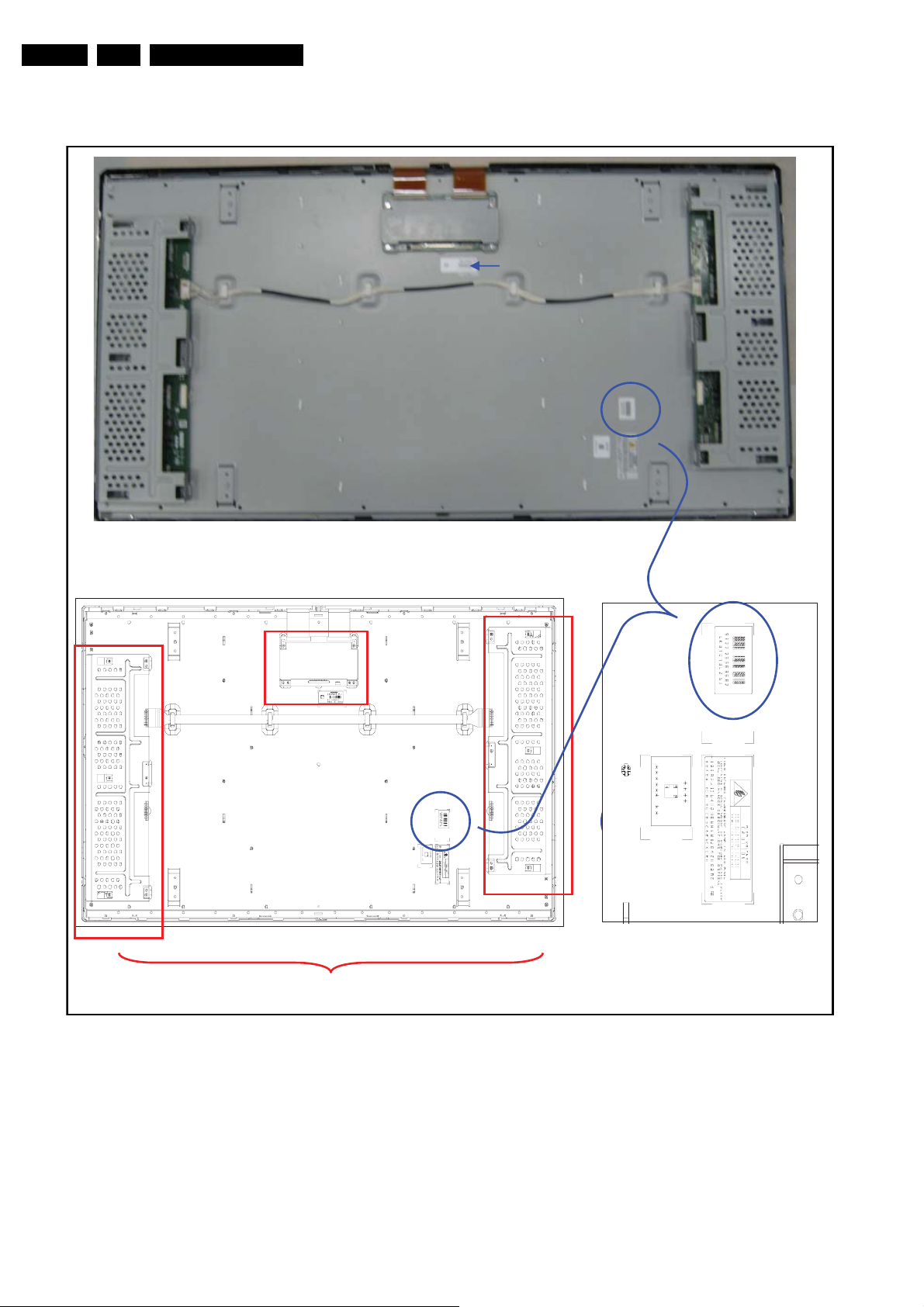
1.4.2 37-inch models
Technical Specifications, Connections, and Chassis Overview
Label of Back light unit
37” module rear view
Control-PWB
37” module rear view
Bar-code label of
complete module
Bar-code label
Inverter-PWB
Figure 1-3 Board and label location (37-inch models)
I_17810_007.eps
280808
Page 5
Technical Specifications, Connections, and Chassis Overview
w
w
w
w
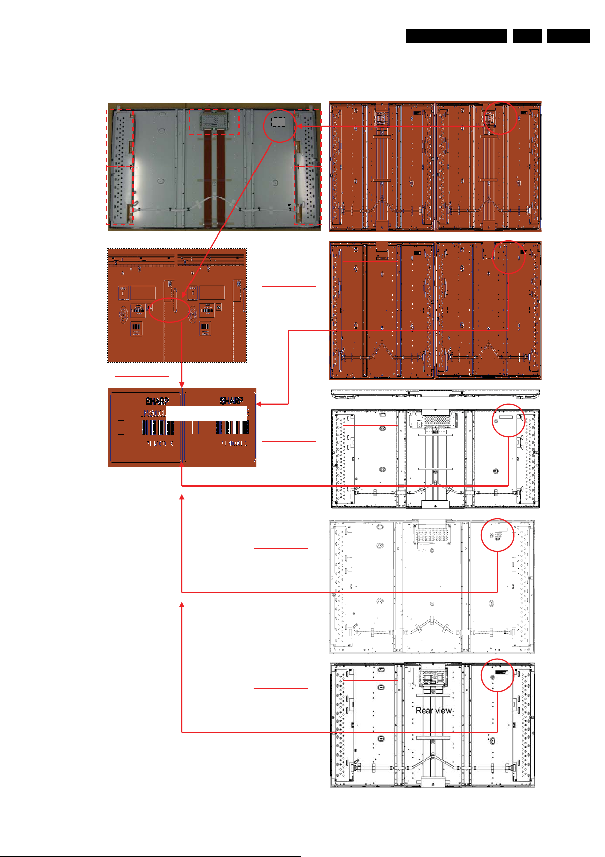
1.4.3 52-inch models
EN 5LCD SHARP 2k8 1.
Inverter
Rear view
LK520D3LZ93
Bar-code label
Control PWB
Inverter
LK520D3LZ83
(Bar-code label
Is same as this
type of Label)
LK520D3LZ93
Rear vie
LK520D3LZ83
Rear vie
LK520D3LZ93
LK520D3LZ33
(Bar-code label
Is same as this
type of Label)
LK520D3LZ13
(Bar-code label
Is same as this
type of Label)
LK520D3LZ9P
(Bar-code label
Is same as this
type of Label)
LK520D3LZ33
Rear vie
LK520D3LZ13
Rear vie
LK520D3LZ9P
I_17812_012.eps
181208
Figure 1-4 Board and label location (52-inch models)
Page 6

EN 6 LCD SHARP 2k82.
Safety Instructions, Warnings, and Notes
2. Safety Instructions, Warnings, and Notes
Index of this chapter:
2.1 General
2.2 Safety Precautions
2.3 Servicing Precautions
2.1 General
Notes:
• Only authorised persons should perform servicing of this
module.
• When using/handling this unit, pay special attention to the
LCD Module: it should not be enforced into any other way
then next rules, warnings, and/or cautions.
• "Warning" indicates a hazard that may lead to death or
injury if the warning is ignored and the product is handled
incorrectly.
• "Caution" indicates a hazard that can lead to injury or
damage to property if the caution is ignored and the
product is handled incorrectly.
2.2 Safety Precautions
2.2.1 Warning
• Do not supply a voltage higher than specified to this
product. This may damage the product or can create
hazardous situations.
• Do not use this product in locations where the humidity is
extremely high, where it may be splashed with water, or
where flammable materials surround it.
• Do not install or use the product in a location that does no
satisfy specified environmental conditions. This may
damage the product or can create hazardous situations.
• If a foreign substance (such as water, metal, or liquid) gets
inside the product, immediately turn “OFF” the power.
Continuing to use the product may cause electric shock or
can create hazardous situations.
• If the product emits smoke and abnormal smell, or makes
an abnormal sound, immediately turn “OFF” the power.
Continuing to use the product may cause electric shock or
can create hazardous situations.
• Do not (dis)connect the connector while power to the
product is “ON”. It takes some time for the voltage to drop
to a sufficiently low level after the power has been turned
“OFF”. Confirm that the voltage has dropped to a safe level
before (dis)connecting the connector.
• Do not pull out or insert the power cable from/to an outlet
with wet hands. It may cause electric shock.
• If the power cable is damaged, or if the connector is loose,
do not use the product, otherwise, this can lead to
hazardous situations or may cause electric shock.
• The LCD Backlight Inverter unit uses a high voltage for the
lamps. Keep the cautions concerning electric shock and do
not touch the device circuitry handling the inverter unit. And
because the capacitors of the device circuitry may remain
charged at the moment of Power “OFF”, standing for 1
minute is required in order to discharge the device circuitry.
2.2.2 Caution
• Do not place this product in a location that is subject to
heavy vibration, or an unstable surface such as an inclined
surface. The product may fall off or fall over, causing
injuries.
• Before disconnecting cable from the product, be sure to
turn off the power. Be sure to hold the connector when
disconnecting cables. Pulling a cable with excessive force
may cause the core of the cable to be exposed or break the
cable, and this can lead to fire or electric shock.
• This product contains glass. If shock, vibration, heat or
distortion is applied to the product, the glass may be
broken.
• If glass surface of the display breaks or is scratched, do not
touched the broken pieces or the scratched with bare
hands. You may be injured.
• LCD Module requires to be handled with special care. LCD
Module is not to be touched with metal or hard materials.
Must not be stressed by heat or mechanical impact.
• There are some particular components on the rear panel of
this product. Skin contact with these components may
cause an electric shock. So, handle with care.
• While moving the product, be sure to turn off the power,
disconnect all cables and watch your step. Dropping the
product may cause injuries from electric shock. So, while
moving the product handle with care.
• When cleaning the panel is necessary, wipe it with a soft
and moistened cloth a neural detergent. Caution on
connector area. Do not use chemicals such as thinner or
benzene.
• LCD Module emits heat from the Lamp, Backlight lamp,
and component parts. Therefore, the environmental
temperature must not exceed 50 deg. C. LCD Module
Backlight Inverter system is driven by high voltage, so it
must avoid conductive materials.
• If repairing components with a lead line, high voltage or
high temperature components must be put out from a lead
line and fix.
• Do not place an object on the surface of the display. The
glass may break or be scratched.
• This product may be damaged if it is subject to excessive
stresses (such as excessive voltage, current, or
temperature). The absolute maximum ratings specify the
limits of these stresses.
• Do not cover or wrap with any covering materials while
power is applied to the product.
• This product is made from various materials such as glass,
metal, and plastic. When discarding it, be sure to contact a
purchase place.
• If a discrepancy occurs due to any arbitrary modification or
disassembly, supplier is not responsible for function,
quality or other items.
• Within the warranty period, general faults may be charged
for depending on responsibility for the faults. You handle
with care
2.3 Servicing Precautions
A colour TFT LCD Module can easily be damaged by both
electrical and mechanical stresses. Users therefore, are
requested to follow the “Servicing precautions of colour TFT
LCD Module” on the following.
2.3.1 System Assembler
• Follow the power sequence: An abnormal power
sequence may cause critical malfunction or electrical
damage.
• Prevent physical stress.
• Prevent overheat:
– High temperatures on the surface of the screen may
cause poor quality. Please use the LCD Module on the
specified temperatures.
– Low temperatures (under 10 deg. C) makes the LCD
Module respond slowly, make the Backlight worse
operated, and will shorten very much the lifetime
accordingly.
• Keep LCD Module dust-free: The LCD Module is
sensitive against dust; it can cause visual or functional
problems.
Page 7

Directions for Use
EN 7LCD SHARP 2k8 3.
• Do not touch TCP area: Do not touch TCP area at any
case. It can cause Driver IC cracks, film cracks, etc. The
TCP is the weakest point of the LCD Module.
• Do not pull Backlight wire: Please do not pull the
Backlight wire, as it can cause the wire to become
disconnected or damaged.
• Check the connections of the Inverter & Backlight
connectors: Incomplete connection can cause burnt in
Backlight connectors or damage the inverter.
• Handle with care:
– Please do not drop, bend, or hit the LCD Module.
– Physical stress can cause defects as broken panels.
• Keep mounting screw length and motor driver’s
torque: Strong motor driver’s torque can make a
mechanical defect on LCD Module. Please keep within the
specifications.
• Do not operate for a long time under the same pattern:
Operating the LCD Module for a long time with the same
video pattern can cause image persistence and can
eventually damage it.
• Defective panels must also be handled with care:
– To prevent making other defects, please handle the
defective LCD Module as a good one.
– Defective LCD Modules must be repaired.
• Do not stack LCD Modules: The LCD Module consists of
fragile components such as TCPs or Glasses. Stacking the
LCD Modules can cause undesired defects.
• Do not provide strong pressure at connecting: Strong
pressure can transfer the force to the TCP, which is the
weakest part of the LCD Module. It eventually can make
the TCP crack or lead to other unexpected defects.
• Let the Backlight Wire at the backside of the LCD
Module: If let the Backlight wire in front of the LCD Module,
the Backlight connector can hurt the surface of the
polariser.
• Never (dis)connect at power “ON”: The LCD Module
consists of CMOS components, which are known as weak
components against EOS. It can damage the product.
• Electro-static discharge can make damage:
– Semi-assembled product should be handled with wrist
strap.
– Earth human body when handle the LCD Module.
– Please do not touch the interface connector pin.
2.3.2 System Assembler/End User
• Keep clean the surface:
– Please wear rubber gloves when you touch the surface
of the LCD Module screen.
– Please use soft and anti-static material with n-Hexane
as cleaner.
• Be careful not to make polariser scratch:
– Surface of polariser is soft, so it’s easily scratched.
– Please do not touch, press or rub on polariser surface
with materials over HB hardness.
• Be careful with swift temperature and humidity
changes: Swift temperature and or humidity change can
make dew condensation or ice, which can cause nonconformance such as malfunctioning.
• Keep out of water:
– Water on in the LCD Module can cause electrical short
or corrosion.
– Please wipe out or dry water carefully.
• Keep the LCD Module free from corrosive gasses:
Corrosive gas can chemically damage the polariser and
the circuitry parts and eventually will cause defects.
• Keep the suitable temperature and humidity:
temperatures and high humidity will shorten the lifetime
High
3. Directions for Use
Not applicable.
Page 8
EN 8 LCD SHARP 2k84.
Mechanical Instructions
4. Mechanical Instructions
Index of this chapter:
4.1 General
4.2 Model LK315D3LZ43
4.3 Model LK315D3LZ73
4.4 Model LK315T3LA33
4.5 Model LK315T3LZ53
4.6 Model LK315T3LZ93
4.7 Model LQ315T3LZ23
4.8 Models LK370D3LZ33, LK370D3LZ43, and LK370T3LZ53
4.9 Model LK520D3LZ13
4.10 Model LK520D3LZ33
4.11 Model LK520D3LZ83
4.12 Model LK520D3LZ93
4.13 Model LK520D3LZ9P
4.1 General
4.1.1 Warnings
• Figures can deviate due to the different module executions.
• During repair, place the set face down on a soft surface
(e.g. on foam bars as mentioned in next paragraph), in
order to prevent damaging the display.
Note: With some chassis, it is possible to measure and
replace the boards while the TV is still on its stand.
• All ICs and many other semiconductors are susceptible to
electrostatic discharges (ESD w). Careless handling
during repair can reduce life drastically. Make sure that,
during repair, you are connected with the same potential as
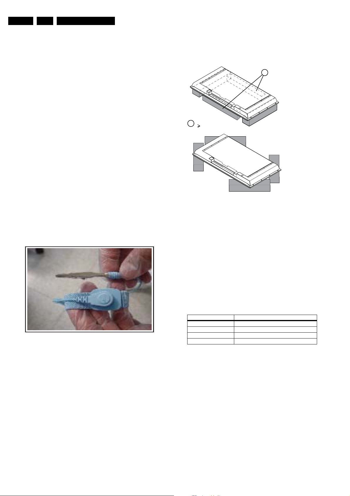
the mass of the set by a wristband with resistance. Keep
components and tools also at this same potential.
4.1.2 Foam Bars
1
Required for sets
1
42"
E_06532_018.eps
171106
Figure 4-2 Foam bars
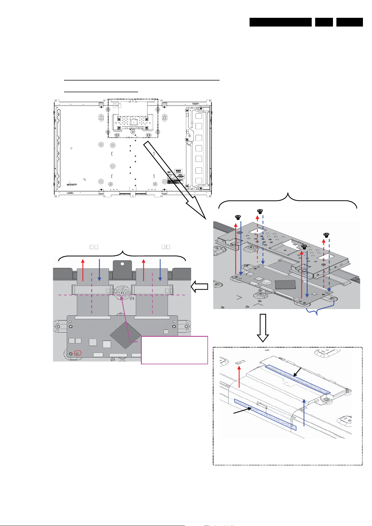
The foam bars (order code 3122 785 90580 for two pieces) can
be used for all types and sizes of flat displays. See figure
“Foam bars” for details. Displays with a size of 42” and larger,
require four foam bars [1]. Ensure that the foam bars are
always supporting the cabinet and never only the display.
Caution: Failure to follow these guidelines can seriously
damage the display!
By laying the TV face down on the (ESD protective) foam bars,
a stable situation is created to perform measurements and
alignments. By placing a mirror under the display, you can
monitor the screen.
H_16920_001.eps
060407
Figure 4-1 ESD wristband
• Be careful during measurements in the high voltage
section. Never pull plugs out under operation conditions,
just to prevent danger caused by electrical sparks.
• Never replace modules or other components while the unit
is switched “on”.
• Connectors “to” and “from” the Inverter Boards must be
thoroughly connected to avoid any electrical sparks during
operation.
4.1.3 Torque Values
Table 4-1 Recommended Torque Values
Screw Type (cross head) Recommended Torque Value
M2 2.0 kg*F ± 0.1 kg*F
M2.5 3.0 kg*F ± 0.2 kg*F
M2.6 3.0 kg*F ± 0.2 kg*F
M3 4.0 kg*F ± 0.2 kg*F
Page 9
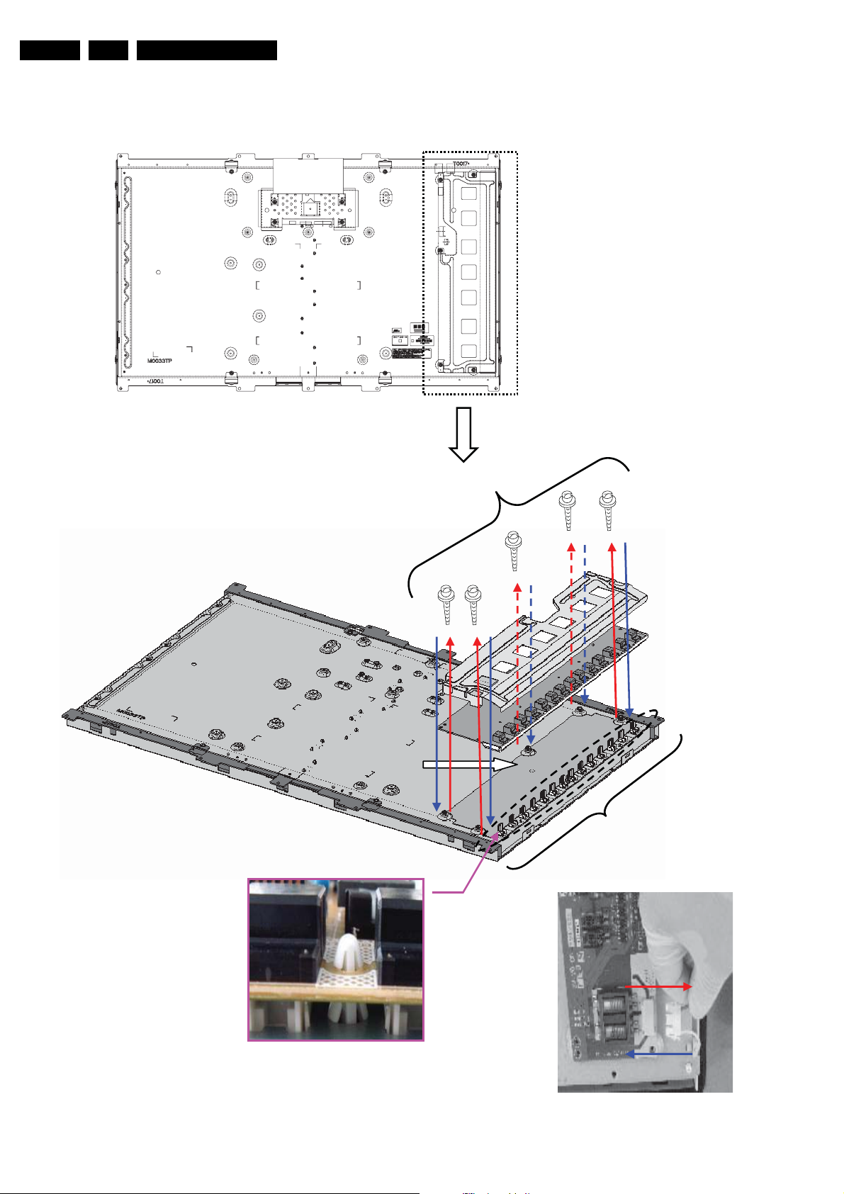
4.2 Model LK315D3LZ43
g
4.2.1 Control Board
T he detaching and installation method of Control-PWB
Model: L Q315T3LZ43
R ea r view
Control-PWB
Mechanical Instructions
Fi
.1 Detach “Screw
at 4 places”
and Cover
EN 9LCD SHARP 2k8 4.
Fig.6 S ecure "Screw
at 4 places"
and Cover
Fig.3Detach “CS-FPC
with F errit e core”
at 2 places
CS-FPC CS-FPC
Inverter
PWB
Fig.4 S ecure “CS-FPC
with F errite core ”
at 2 places
Ferrite coreFerrite core
L ocate C S- FP C with
its center line and
Ferrite Core's center
line are aligne d
Rearview
Fig.2 Detach
P rotection sheet
CS-FPCprotection sheet
Cover
Inverter
PWB
Locate new
Inverter-PW B on
fixing pos ition
Double-sided tape
Double-sidedtape
Fig.5 Secure Protectionsheet
1. F it t he tape e dge jus t below
the cutoutpartofC-PWBcover
2. E ns ure it is not sticking out of
Bezel edge
I_17811_006.eps
250908
Figure 4-3 (Dis)assembly method for the Control Board
Page 10
EN 10 LCD SHARP 2k84.
r
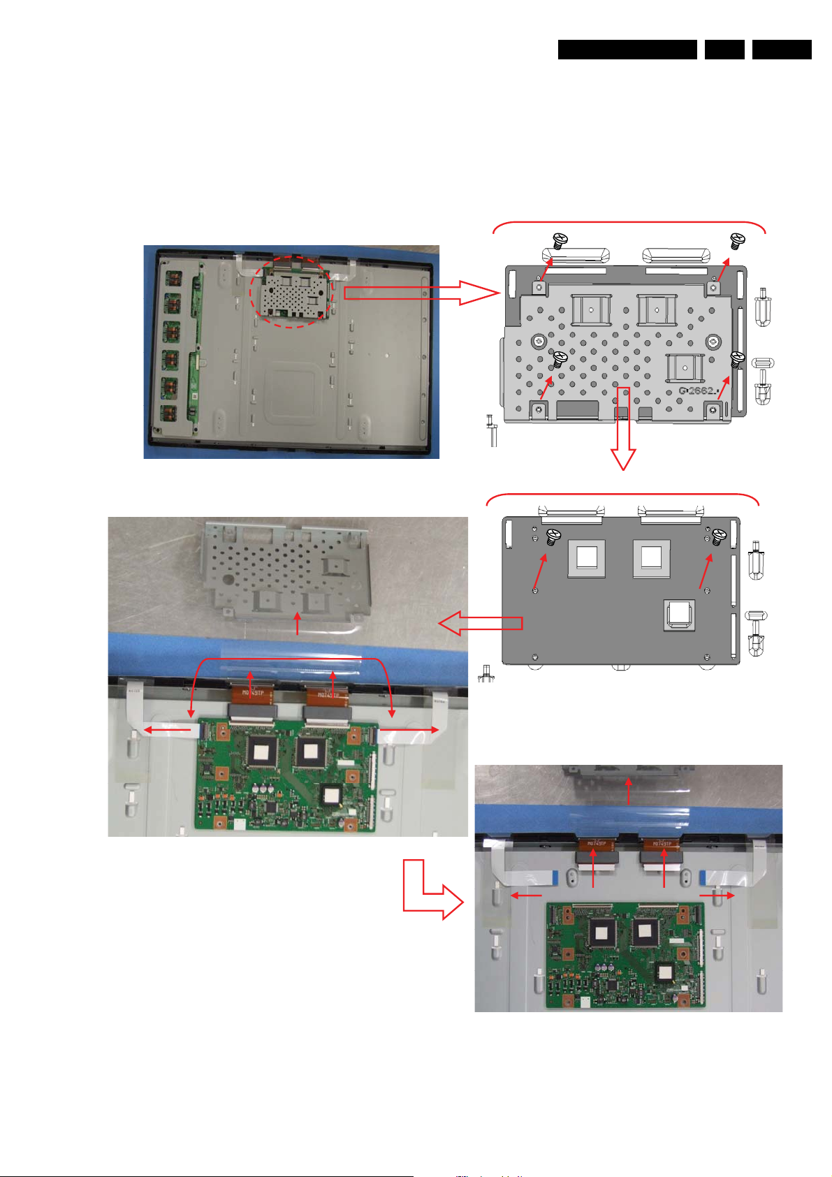
4.2.2 Inverter Board
Mechanical Instructions
Inverter
Rearview
Fig.4 Secure "Screw
at 5 places"
and Cover
Fig.1 Detach “Screw
at 5 places”
and Cover
Locate new
Inverter-PW B
on fixing position
C onfirm the hook parts
are open out
Inverter-PW B
Fig.2 Detach
Lamp-connector
at 7 places
Fig.3 Secure
Lamp-connecto
at 7 places
Figure 4-4 (Dis)assembly method for the Inverter Board(s)
I_17811_007.eps
250908
Page 11
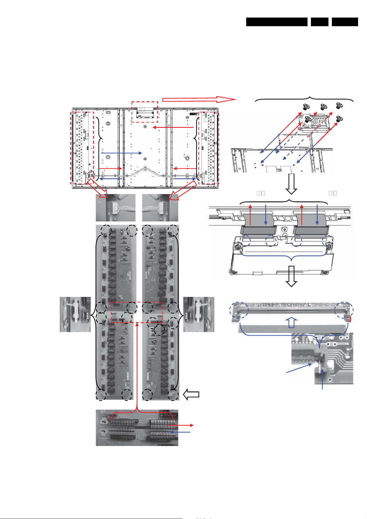
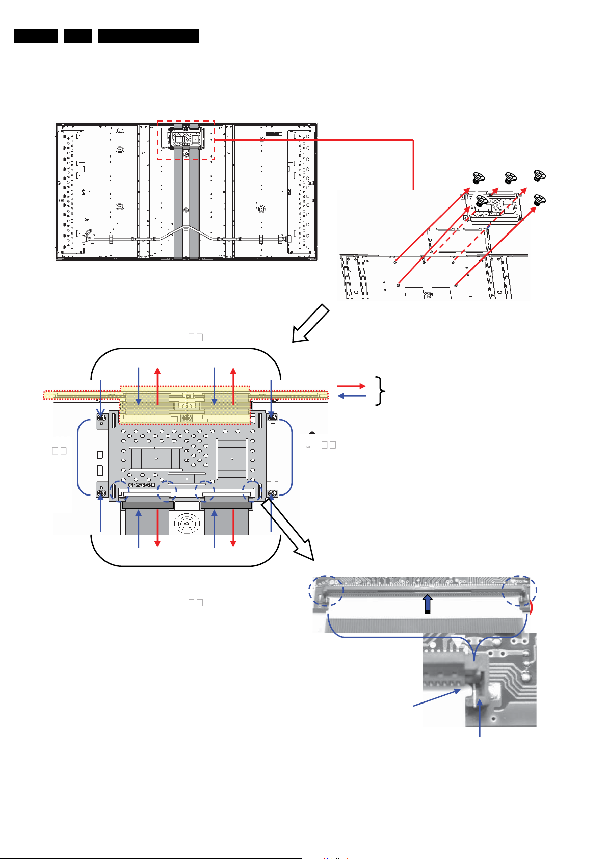
4.3 Model LK315D3LZ73
4.3.1 Control Board
Mechanical Instructions
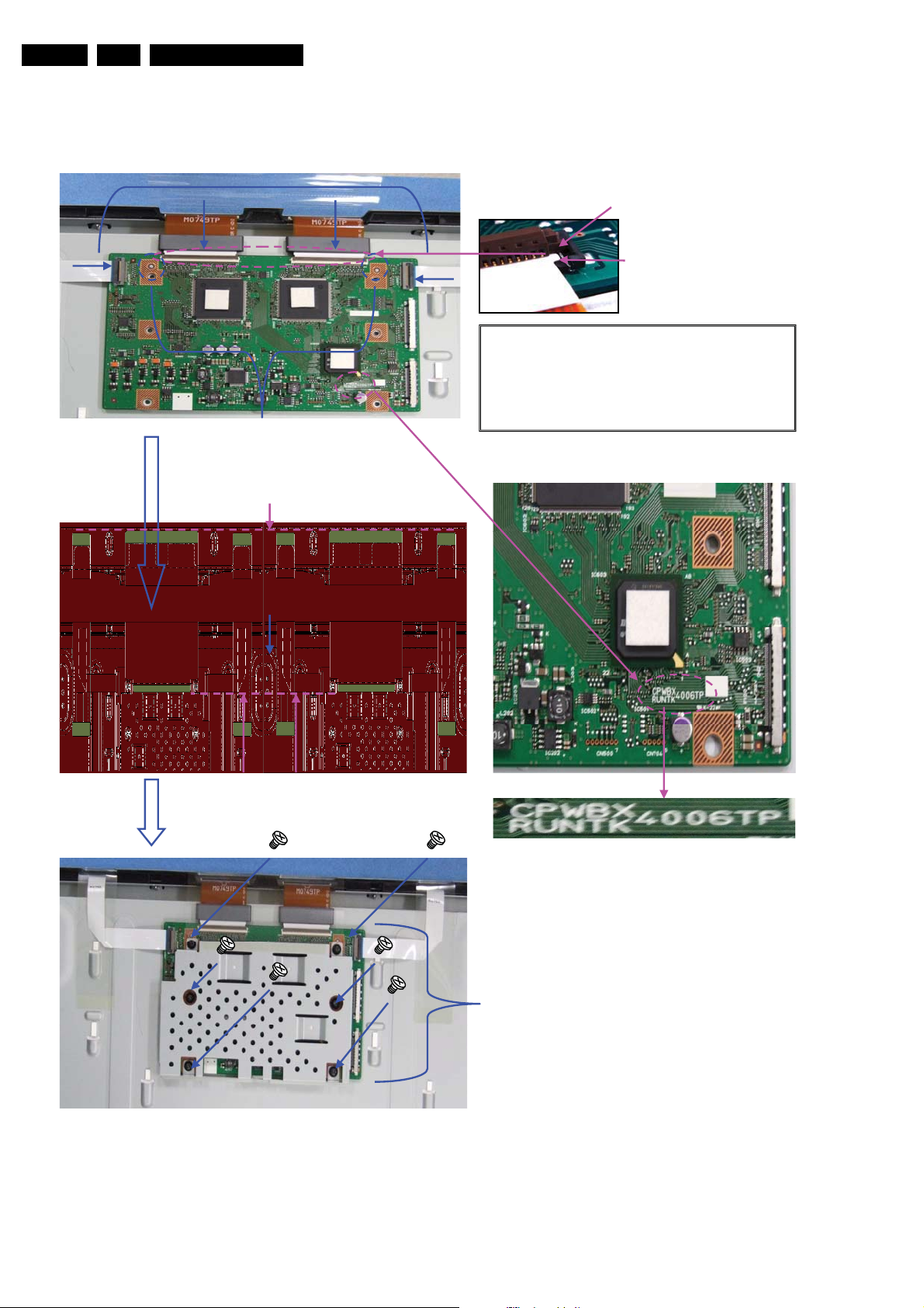
Fig.1: Detach “Screw at 4 places” and Cover
EN 11LCD SHARP 2k8 4.
Fig 3. Detach Protection sheet
Fig 4. Detach “CS-FPC at 4 places” and Ferrite core
Ferrite core
Ferrite core
Fig 2. Detach "Screw at 2 places" and Control-PWB
The condition of detection CS-FPC cable
and Protection sheet
Protection
sheet
Figure 4-5 (Dis)assembly method for the Control Board -1-
I_17812_002.eps
031208
Page 12
EN 12 LCD SHARP 2k84.
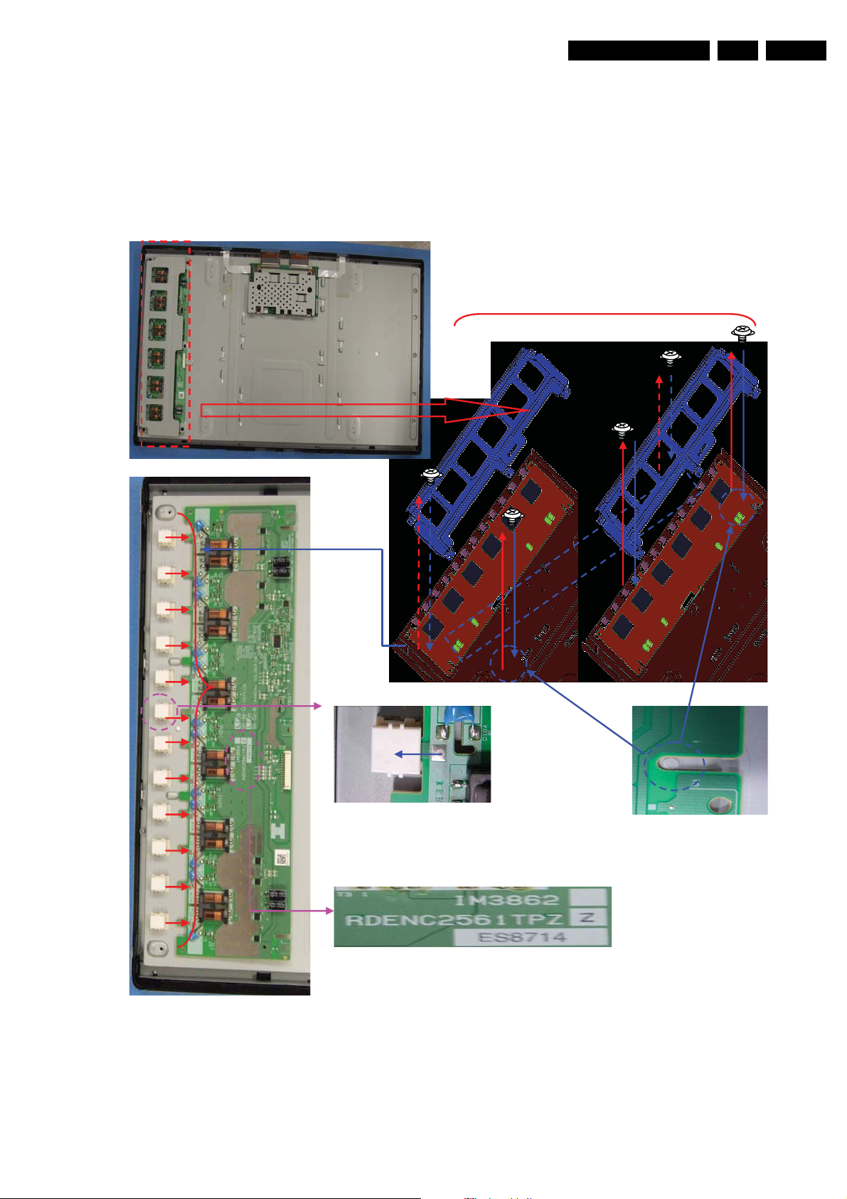
Fig 5. Secure “CS-FPC at 4 places” and Ferrite core
Mechanical Instructions
onvex part
of FPC
Connector
Protrusion
NOTE: when attaching the CS-FPC
* Attach CS-FPC by hooking its convex parts
of FPC to Connector protrusions
* Fit it to the end and close the lid firmly
* Distinguish the front and back sides of the FPC
Locate: “new Control-PWB”
on original fixing position
Ensure it is not sticking out of Bezel edge
Protection sheet
Fig 6. Secure Protection sheet
Protection sheet
Sticki ng position
(Cutout part of PWB Cover)
The position of code described in Control-PWB
Fig.7: Secure Screw at 2 places
for Control-PWB
Fig 7. Secure Screw at 4 places
for Cover
Figure 4-6 (Dis)assembly method for the Control Board -2-
I_17812_003.eps
031208
Page 13
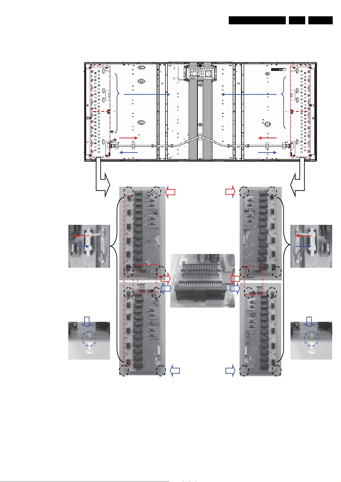
4.3.2 Inverter Board
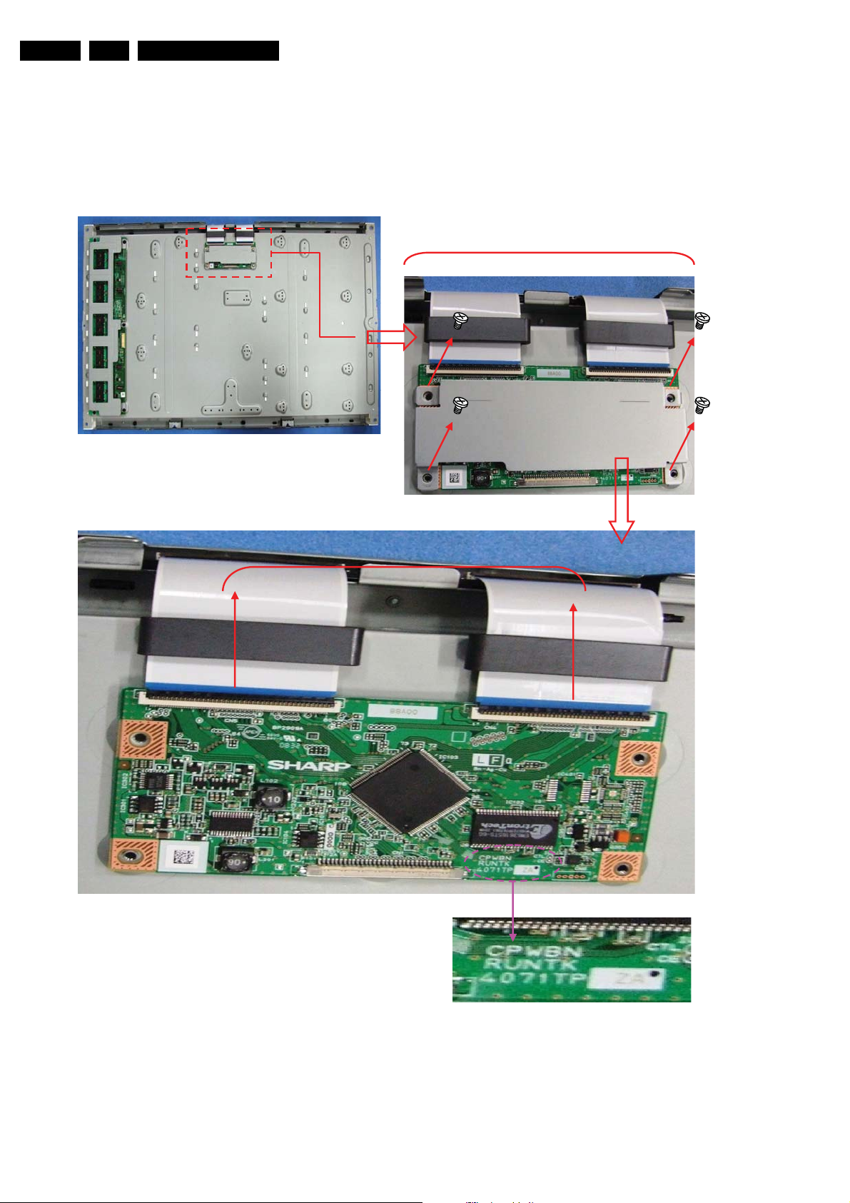
A
* Fit Inverter-PWB
* Fit Inverter-cover
*Fix Inverter-PWB and cover with screw
1. Confirm the positioning PIN
2. Slide the INV-UNIT
Mechanical Instructions
Fig.1: Detach “Screw at 5 places” and Cover
Fig.4: Secure “Screw at 5 places” and Cover
EN 13LCD SHARP 2k8 4.
Fig.2: Detach “Lamp connector
at 12 places and Inverter-PWB
Fig.3: Secure “Lamp connector
t 12 places and Inverter-PWB
The position of code described in Inverter-PWB
Locate “new Inverter-PWB”
on original fixing position
I_17812_004.eps
031208
Figure 4-7 (Dis)assembly method for the Inverter Board(s)
Page 14
EN 14 LCD SHARP 2k84.
4.4 Model LK315T3LA33
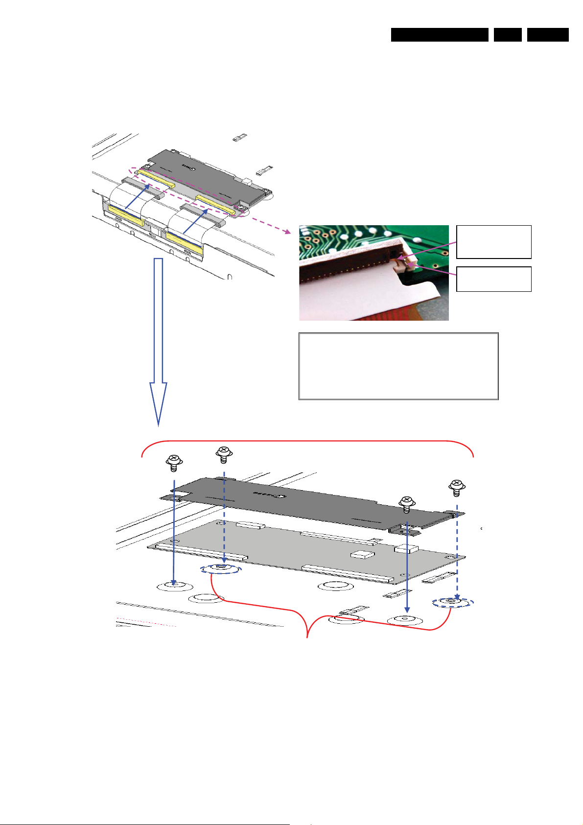
4.4.1 Control Board
Mechanical Instructions
Control-PWB
Ferrite core
CS-FPC
Fig.1: Detach “Screw at 4 places” and Cover
Control-PWB
Fig 2 Detach “CS-FPC at 2places” and Ferrite core
Ferrite core
CS-FPC
The position of code described in Control-PWB
Figure 4-8 (Dis)assembly method for the Control Board -1-
I_17812_007.eps
041208
Page 15
Mechanical Instructions
g
3: Secure “CS-FPC at 2places” and Ferrite core
Fi
EN 15LCD SHARP 2k8 4.
Protrusion at
the both sides
of CS-FPC
Protrusion
of Connector
NOTE: when attaching the CS-FPC
* Attach CS-FPC by hooking its convex parts
of FPC to Connector protrusions
* Fit it to the end and close the lid firmly
* Distinguish the front and back sides of the FPC
Fig.4: Secure “Screw at 4 places” and Cover
Locate: “new Control-PWB “
on original fixing position
Figure 4-9 (Dis)assembly method for the Control Board -2-
I_17812_008.eps
041208
Page 16
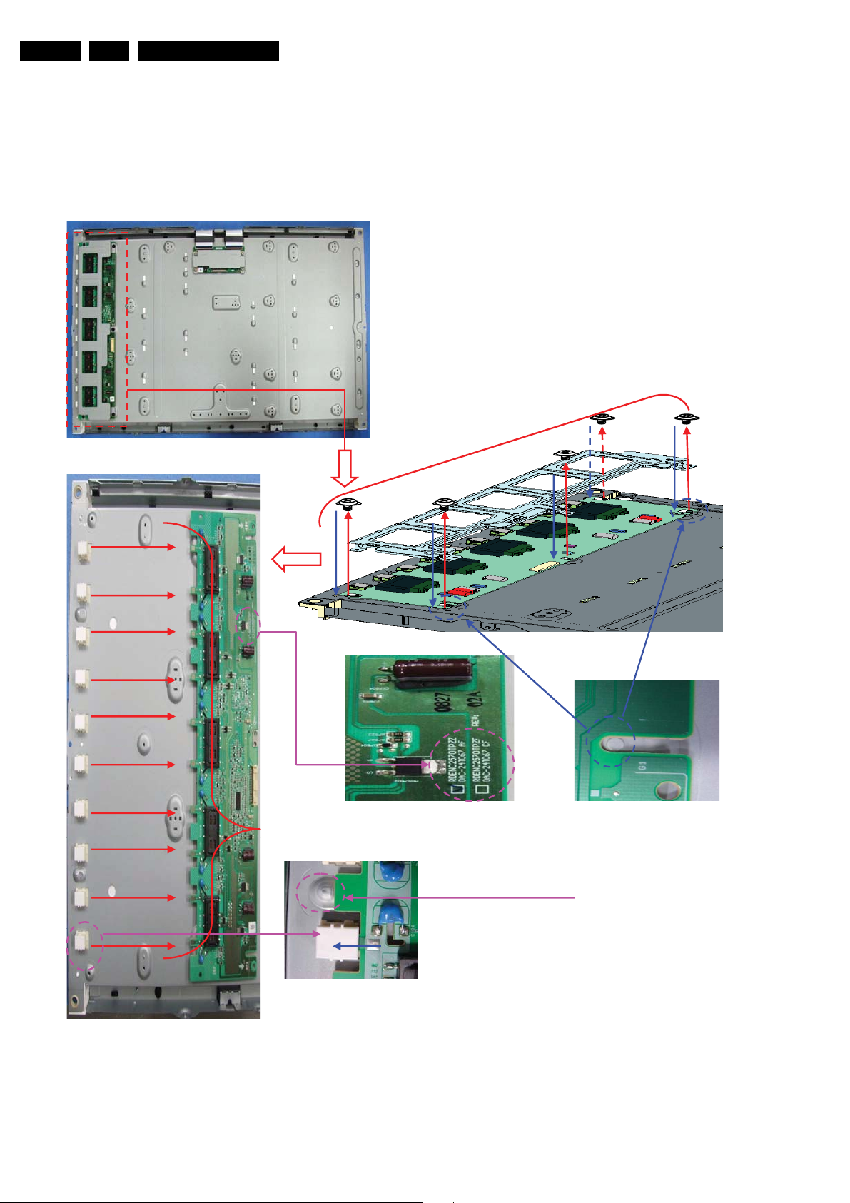
EN 16 LCD SHARP 2k84.
A
4.4.2 Inverter Board
Mechanical Instructions
Fig.1: Detach “Screw at 5 places” and Cover
Fig.4: Secure “Screw at 5 places” and Cover
The position of code
described in Inverter-PWB
Fig.2: Detach “Lamp connector
at 10 places and Inverter-PWB
Slide the InverterPWB until stopper
Fig.3: Secure “Lamp connector
t 10 places and Inverter-PWB
I_17812_009.eps
041208
Figure 4-10 (Dis)assembly method for the Inverter Board(s)
Page 17
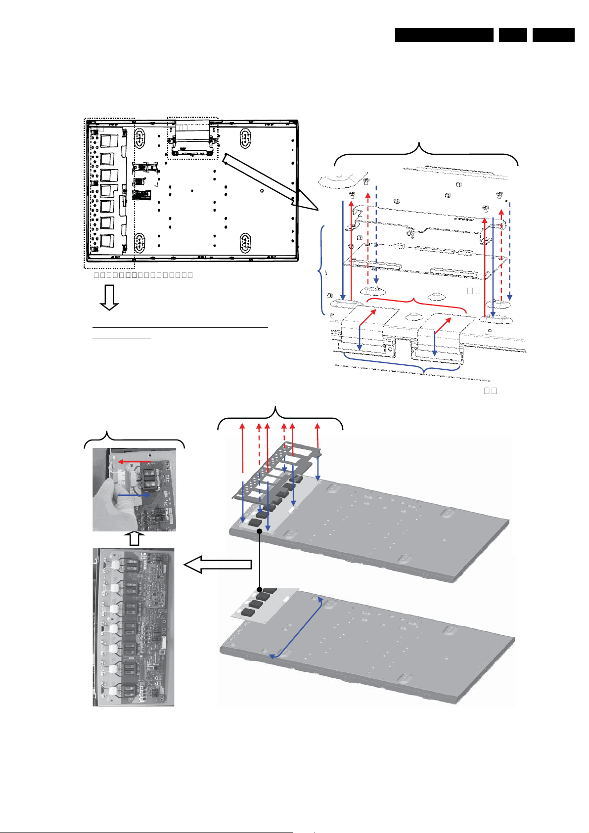
4.5 Model LK315T3LZ53
4.5.1 Control and Inverter Board
Mechanical Instructions
EN 17LCD SHARP 2k8 4.
Control-PWB
Rearview
T he detaching and installation method of
Inverter-PW B
Fig.2 Detach
Lamp-connector
at 7 places
Fig.3 Secure
Lamp-connector
at 7 places
Fig.1 Detach “Screw
at 6 places”
and Cover
Locate new
Inverter-PWB on
fixing position
Fig.4 Secure "Screw
at 6 places"
and Cover
Fig.1Detach “Screw
at 4 places”
and Cover
Cover
Contorl-PWB
Fig.3 Detach
“CS -F PC ”at 2 places
CS-FPC
Fig.4 Secure
“CS -F PC ”at 2 places
Fig.6 S ecure "Screw
at 4 places"
and Cover
CS-FPC
Inverter
PWB
Cover
Inverter
PWB
Rearview
Locate new
Inverter-PWB on
fixing position
I_17811_005.eps
250908
Figure 4-11 (Dis)assembly method for the Control and Inverter Board
Page 18
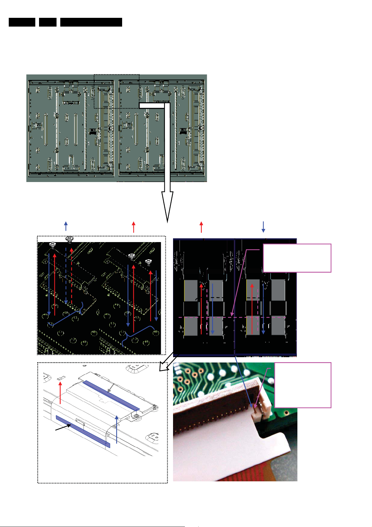
EN 18 LCD SHARP 2k84.
r
4.6 Model LK315T3LZ93
4.6.1 Control Board
Rear view
Mechanical Instructions
Control-PWB
Fig.6 Secure "Screw
at 4 places"
and Cover
Cove
Contorl-PWB
Locate new
Inverter-PWB on
fixing position
Fig.2 Detach
Protection sheet
CS-FPC protection sheet
Fig.1 Detach “Screw Fig.4 Secure “CS-FPC
at 4 places” with Ferrite core”
and Cover
Fig.3 Detach “CS-FPC
with Ferrite core”
at 2 places
at 2 places
Locate CS-FPC with
its center line and
Ferrite Core's center
line are aligned
Ferrite core
Ferrite core
CS-FPC CS-FPC
The FPC salient is
Double-sided tape
put in the concave
connector part,
and the connector
is locked properly
Double-sided tape
Fig.5 Secure Protection sheet
1. Fit the tape edge just below
the cutout part of C-PWB cover
2. Ensure it is not sticking out of
Bezel edge
Figure 4-12 (Dis)assembly method for the Control Board
CS-FPC
I_17811_003.eps
250908
Page 19
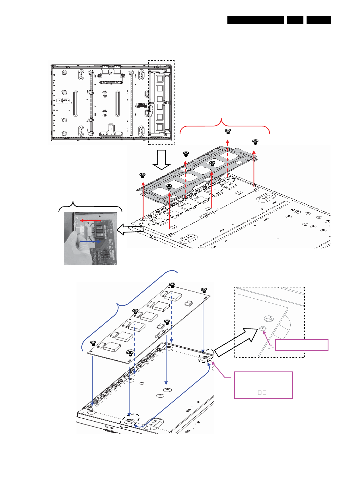
4.6.2 Inverter Board
Rearview
Fig.2 Detach
Lamp-connector
at 6 places
Fig.3 Secure
Lamp-connector
at 6 places
Mechanical Instructions
Inverter
Cover
EN 19LCD SHARP 2k8 4.
Fig.1Detach“Screw
at 6 places”
and Cover
Fig.4 Secure "Screw
at 6 places"
and Cover
Inverter
PWB
Rearview
Inverter-PWB
Positioning PIN
Locate “new
Inverter-PWB”
on original fixing
pos iti on
Figure 4-13 (Dis)assembly method for the Inverter Board(s)
I_17811_004.eps
250908
Page 20
EN 20 LCD SHARP 2k84.
r
r
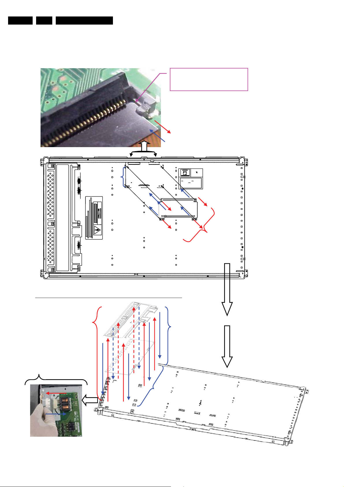
4.7 Model LQ315T3LZ23
4.7.1 Control and Inverter Board
Mechanical Instructions
The FPC salient is inserted
and locked in the connector
Fig.3 Detach
“CS-FPC”
at 2 places
CS-FPC
Fig.4 Secure
“CS-FPC”
at 2 places
Locate
newControl-PWB
on fixing position
Fig.6 Secure
"Screw
at 4 places"
and Cover
Inverte
PWB
Rear view
The detaching and installation method of Inverter-PWB
䌍䌁䌔䌅䌒䌉䌁䌌㩷 䌉䌎䌆䌏䌒䌍䌁䌔䌉䌏䌎
䌏䌐䌔䌉䌃䌁䌌㩷䌆䌉䌌䌍䋺䋾䌐䌃䋬䌐䌅䌓䌔䋬䌁䌋䌕䌒䋭䌘䋬䌐䌃䋼
䌌䌅䌎䌓㩷䌆䌉䌌䌍䋺䋾 䌐䌅䌔䋬䌁䌋䋭䌘䋼
䌄䌉䌆䌆䌕䌓䌅䌒㩷 䌓䌈䌅䌅䌔䋺䋾䌐䌅䌔䋼
䌄䌉䌆䌆䌕䌓䌅䌒㩷 䌂䌏䌁䌒䌄䋺䋾䌍䌍䌁䋯䌓䋼
䌒䌅䌆䌌䌅䌃䌔䌏䌒䋺䋾䌐䌅䌔䋼
Fig.1 Detach
“Screw
at 4 places”
and Cover
Fig.1 Detach
“Screw
at 6 places”
and Cover
Fig.2 Detach
Lamp-connector
at 9 places
Fig.3 Secure
Lamp-connector
at 9 places
Cove
Fig.4 Secure
“Screw
at 6 places”
and Cover
Inverter-PWB
Locate new
Inverter-PWB
on fixing position
Figure 4-14 (Dis)assembly method for the Control and Inverter Board
Rear view
I_17811_002.eps
250908
Page 21
Mechanical Instructions
(
)
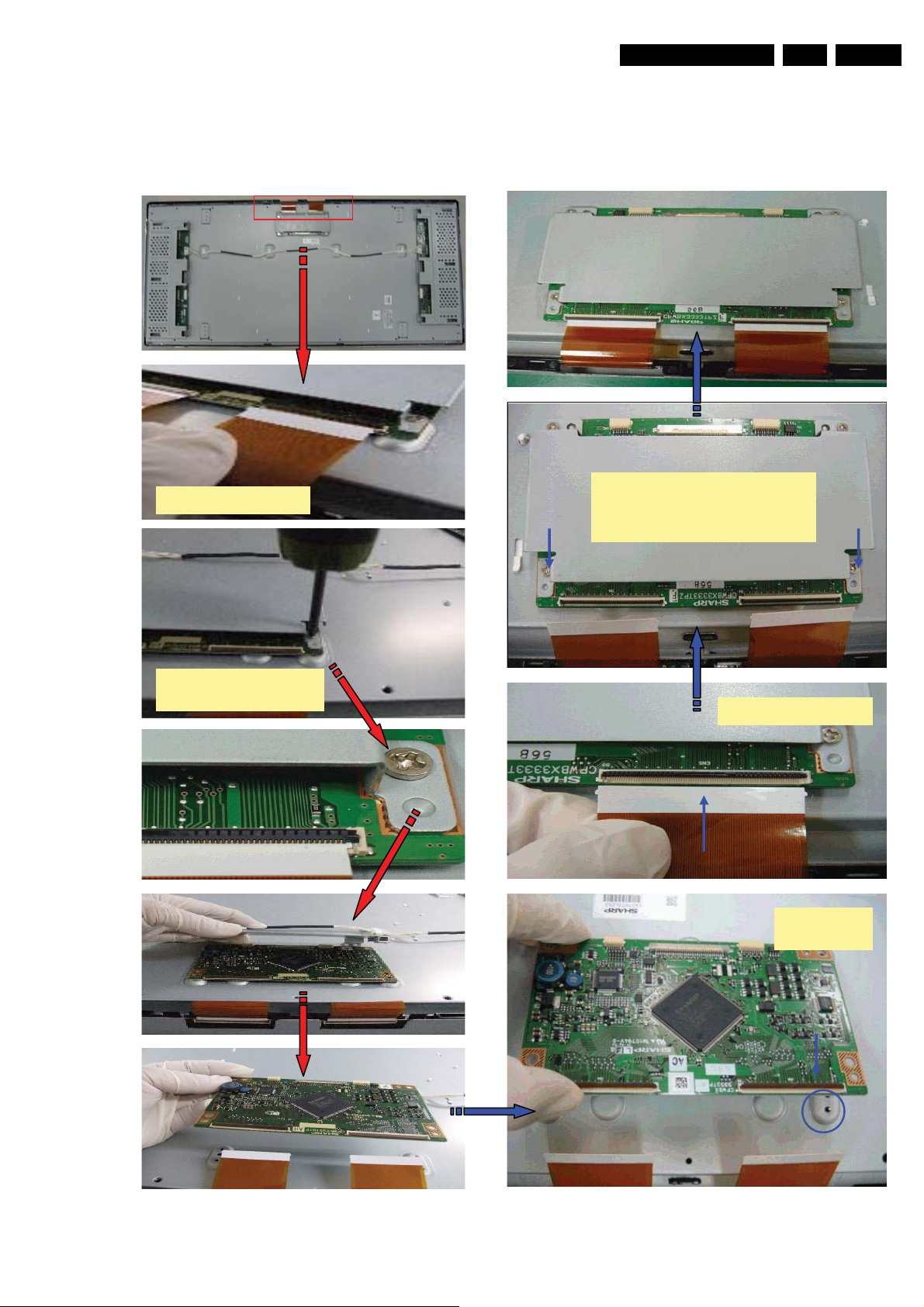
4.8 Models LK370D3LZ33, LK370D3LZ43, and LK370T3LZ53
4.8.1 Control Board
EN 21LCD SHARP 2k8 4.
Fig-1: Detach CS-FPC’s
Fig-2: Detach screws
and cover of Control-PWB
Fig-5: Secure cover of Control-PWB
and thighten screws.
Torque value of screws is
0.392±0.02 N㨯m
4±0.2kgf㨯cm
Fig-4: Secure CS-FPC
Fig-3: Place
Control-PWB
I_17810_008.eps
280808
Figure 4-15 (Dis)assembly method for the Control Board
Page 22
EN 22 LCD SHARP 2k84.
p
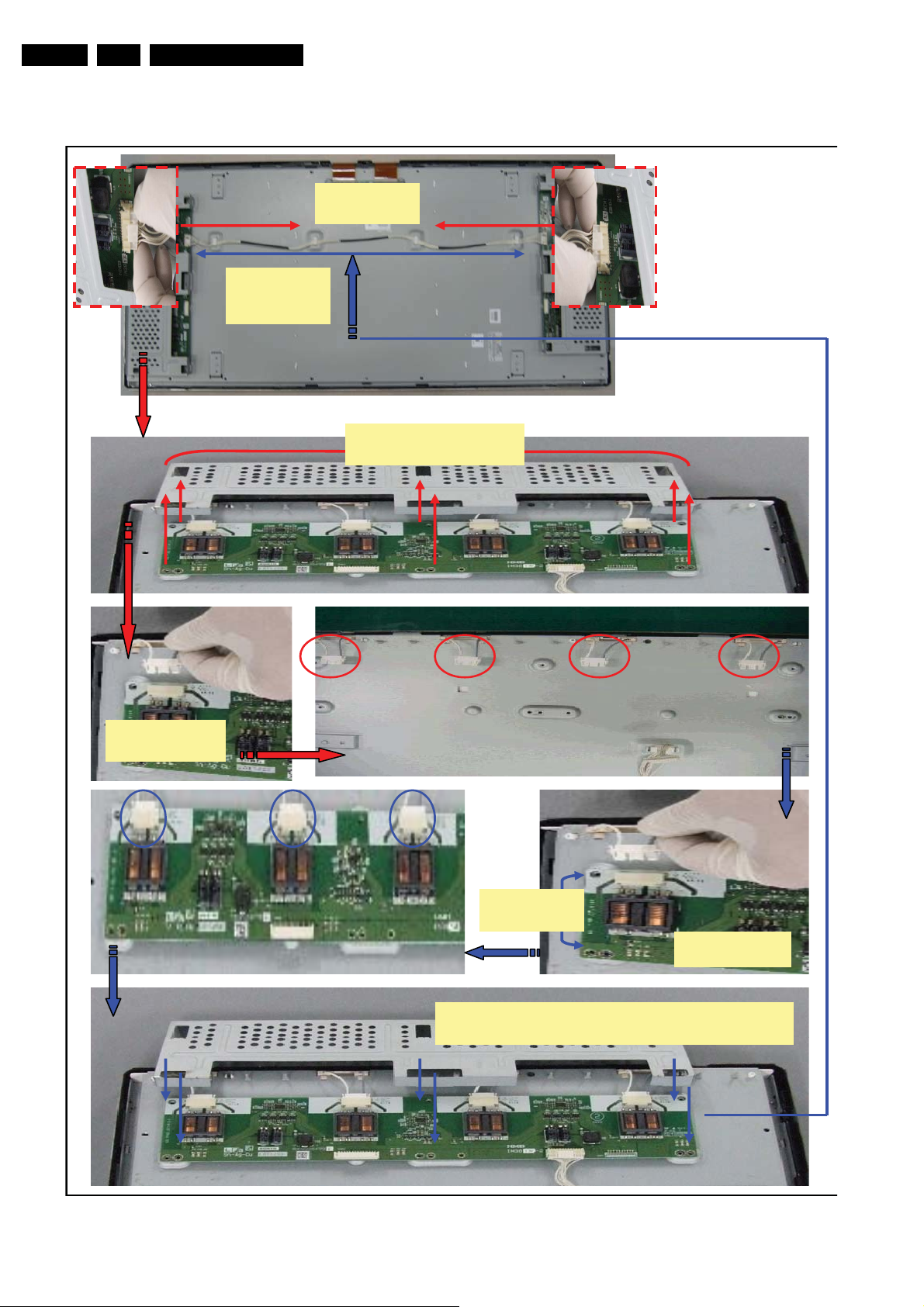
4.8.2 Inverter Board
Mechanical Instructions
Fig-1: Detach
Inverter-cable
Fig-7: Secure
Inverter-cable
with clip
37” module rear view
Fig-2: Detach screw
and cover of inverter-PWB
Cover of inverter-PWB
Fig-3: Detach
Lamp-connectors
Fig4: Place
Inverter-PWB
Fig-5: Secure
Lamp-connectors
Fig-6: Secure cover of Inverter-PWB and thighten screws.
Torque value of screws is 0.392±0.02 N㨯m(4±0.2kgf㨯cm)
Cover of inverter-PWB
Figure 4-16 (Dis)assembly method for the Inverter Board(s)
I_17880_009.e
28080
Page 23
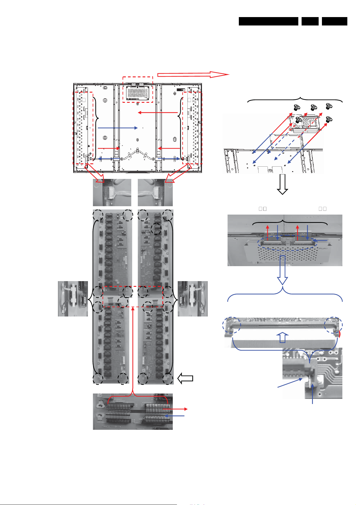
4.9 Model LK520D3LZ13
g
4.9.1 Control and Inverter Boards
Mechanical Instructions
EN 23LCD SHARP 2k8 4.
R ea r view
Fig-2:Detachscrew
at 4 places each
and both of cover
Fig-1:Detach
Inverter-cable
-8: Secure
Fi
Inverter-cable
R DENC2305TPZF
(master side)
Fig.4 Secure "Screw
at 4 places each
and both of cover
R DENC2307TPZF
C3C,C!C6C%
C3C,C!C6C%
(
side)
C3C,C!C6C%C3C,C!C6C%
Fig.1Detach
“Screw
at 5 places”
and Cover
Control-PWB
Locate newControl-PWB
on fixing position
Fig.3Detach “CS-FPC
with F errit e core”
at 2 places
F errite c ore F errite c ore
Fig.6 S ecure
"Screw
at 5 places"
and Cover
Cover
Fig.4Secure “CS-FPC
with F errit e core”
at 2 places
Fig-4: Detach
Lamp-connector
6placesofeach
Fig-5 Secure
Lamp-connector
6placesofeach
R DENC2306TPZF
(
side)
㝄㙻㓠㝾㖋
㝄㙻㓠㝾㖋
㝄㙻㓠㝾㖋㝄㙻㓠㝾㖋
R DENC2308TPZF
(slave s ide)
Fig-4:Detach
Lamp-connector
6placesofeach
Fig-5 Secure
Lamp-connector
6placesofeach
F ig-7: S ecure screw
at 4 places each
and both of cover
Fig-3:Detach
connection-wire
Fig-6:Secure
connection-wire
Cover
Ferrite core
The FPC salient is put in the concave connector
part, and the connector is locked properly
CS-FPC(43)ΩQPW B M0509T PZZ
Convex
connector part
Concave
connector part
I_17811_021.eps
250908
Figure 4-17 (Dis)assembly method for the Control and Inverter Boards
Page 24
EN 24 LCD SHARP 2k84.
g
g
4.10 Model LK520D3LZ33
4.10.1 Control and Inverter Boards
Mechanical Instructions
Rearview
Fig-2: Detach screw
at 4 places each
and both of cover
Fig-1: Detach
Inverter-cable
Fig-8:Secure
Inverter-cable
R DENC2305TPZF
(master side)
.4 S ecure "Screw
Fi
at 4 places each
and both of cover
R DENC2307TPZF
(C3C,C!C6C%
C3C,C!C6C%side)
C3C,C!C6C%C3C,C!C6C%
Fig.1Detach
“Screw
at 5 places”
and Cover
Control-PWB
Locate newControl-PW B
on fixing position
Fig.3 Detach “CS-FPC
with F errite core”
at 4 places
Ferrite core F errite core
Fig.6 S ecure
"Screw
at 5 places"
and Cover
Cover
Fig.4 Secure “CS-FPC
with F errite core”
at 4 places
Fig-4:Detach
Lamp-connector
6places ofeach
Fig-5 Secure
Lamp-connector
6places ofeach
R DENC2306TPZF
(㝄㙻㓠㝾㖋
㝄㙻㓠㝾㖋side)
㝄㙻㓠㝾㖋㝄㙻㓠㝾㖋
R DENC2308TPZF
(slave s ide)
-4: Detach
Fi
Lamp-connector
6places ofeach
Fig-5 Secure
Lamp-connector
6places ofeach
Fig-7:Secure screw
at 4 places each
and both of cover
Fig-3:Detach
connection-wire
Fig-6:Secure
connection-wire
C S-FP C protection sheet
Fig.2 Detach
P rotection sheet
Fig.5 S ecure Protection sheet
1. F it the tape e dge just below
the cutoutpartofC-PWBcover
2. E ns ure it is not s ticking out of
Bezeledge
The FPC salient is put in the concave connector
part, and the connector is locked properly
CS-FPC (43)ΩQPW B M 0509TPZ Z
Convex
connector part
Concave
connector part
I_17811_020.eps
250908
Figure 4-18 (Dis)assembly method for the Control and Inverter Boards
Page 25
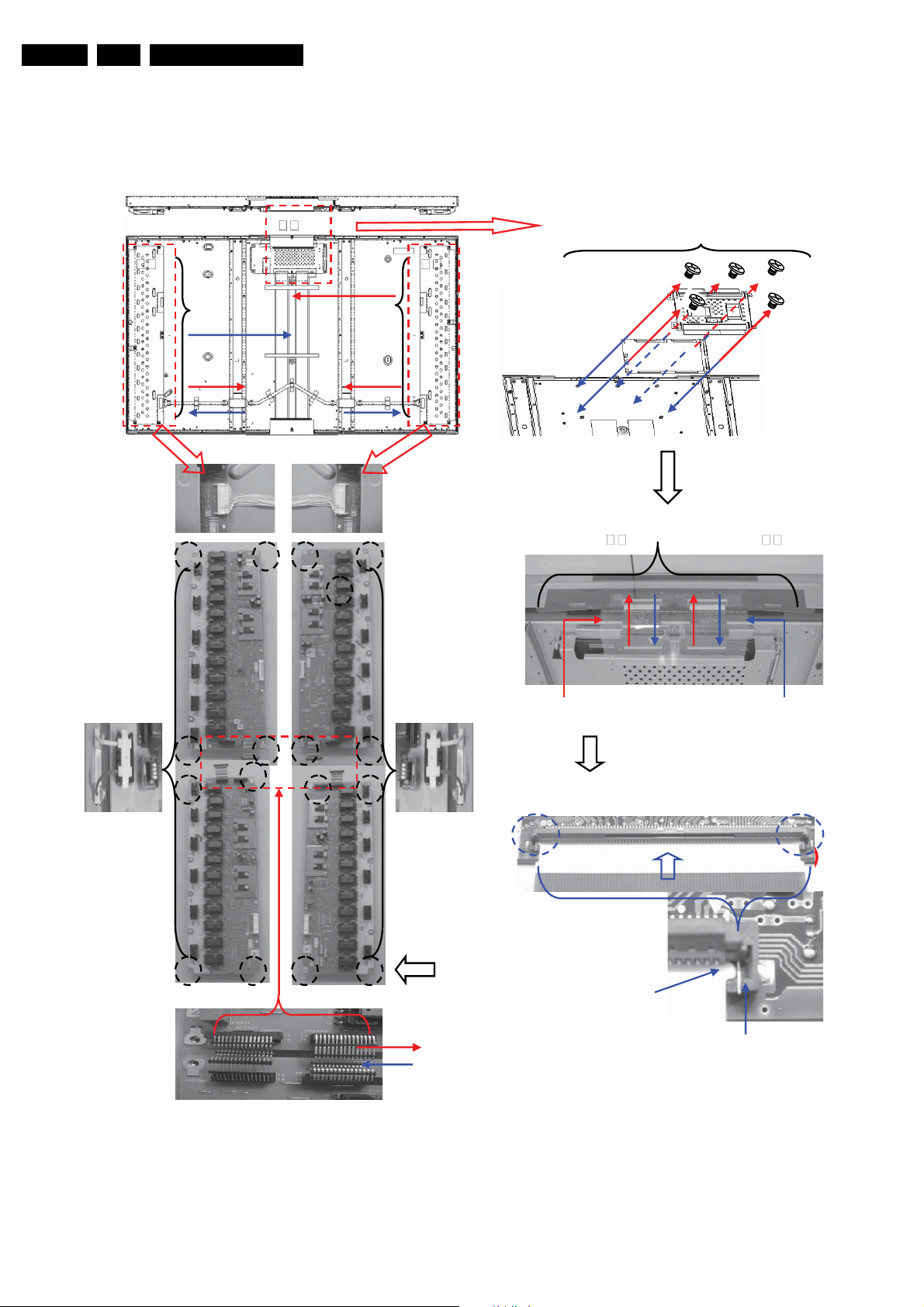
4.11 Model LK520D3LZ83
g
4.11.1 Control and Inverter Boards
Mechanical Instructions
EN 25LCD SHARP 2k8 4.
Rearview
Fig-2: Detach screw
at 4 places each
and both of cover
Fig.4 Secure "Screw
Inverter Inverter
at 4 places each
and both of cover
Fig-1:Detach
Inverter-cable
Fig-8: Secure
Inverter-cable
R DENC2542TPZ
(slave s ide)
R DENC2544TPZ
(slave s ide)
Fig.1 Detach
“Screw
at 5 places”
and Cover
Control-PWB
L ocate newCon tr ol-PW B
on fixing position
Fig.3 Detach “CS-FPC
with F errite core”
at 2 places
F errite c ore Ferrite core
Fig.6Secure
"Screw
at 5 places"
and Cover
Cover
Fig.4 Secure “CS-FPC
with F errite core”
at 2 places
Fig-4:Detach
Lamp-connector
6places ofeach
Fig-5 Secure
Lamp-connector
6places ofeach
R DENC2543TPZ
(master-1 side)
R DENC2545TPZ
(master-2 side)
-4: Detach
Fi
Lamp-connector
6places ofeach
Fig-5 Secure
Lamp-connector
6places ofeach
Fig-7:Secure screw
at 4 places each
and both of cover
Fig-3:Detach
connection-wire
Fig-6:Secure
connection-wire
Control-PWB
The FPC salient is put in the concave connector
part, and the connector is locked properly
CS-FPC (43)ΩQPW B M0509TPZ Z
Convex
connector part
Concave
connector part
I_17811_019.eps
250908
Figure 4-19 (Dis)assembly method for the Control and Inverter Boards
Page 26
EN 26 LCD SHARP 2k84.
g
t
g
4.12 Model LK520D3LZ93
4.12.1 Control Board
Mechanical Instructions
Fig.1 Detach
“Screw
at 5 places”
and Cover
Cover
Control-PWB
L oc ate ne wC ontr ol-PW B
on fixing position
Fig.3 Detach “CS-FPC
with F errite core”
at 4 places
Ferrite core Ferrite core
CS-FPCprotection sheet
Cover
Ferrite core
Ferrite core
Fig.4 Secure “CS-FPC
with F errite core”
at 4 places
Fi
.2Detach
P rotection sheet
Fig.5 Secure Protection shee
1. F it the tape e dge jus t below
the cutoutpartofC-PWBcover
2. E ns ure it is not sticking out of
Ferritecore
Fi
.6 S ecure "Screw
Bezeledge
at 4 places"
and Cover
The FPC salient is put in the concave connector
part, and the connector is locked properly
CS-FPC(43)ΩQPW B M0509TPZZ
Convex
connector part
Concave
connector part
I_17811_017.eps
250908
Figure 4-20 (Dis)assembly method for the Control Board
Page 27
4.12.2 Inverter Board
g
Mechanical Instructions
Inverter Inverter
R ea r view
Fig.4 S ecure "Screw
at 4 places each"
and both of cover
EN 27LCD SHARP 2k8 4.
Fig-4:Detach
Lamp-connector
6placesofeach
Fig-5 Secure
Lamp-connector
6placesofeach
Fig-1:Detach
Inverter-cable
Fig-8:Secure
Inverter-cable
R DENC2542TPZ
(slave s ide)
Fig-2: Detach screw
at 4 places each
and both of cover
Fi
-3: Detach
connection-wire
Fig-1:Detach
Inverter-cable
Fig-8:Secure
Inverter-cable
R DENC2544TPZ
(slave s ide)
Fig-4:Detach
Lamp-connector
6placesofeach
Fig-5 Secure
Lamp-connector
6placesofeach
Locate
Inverter-PWB
on fixing position
Fig-6:Secure
connection-wire
F ig-7: S ecure screw
at 4 places each
and both of cover
R DENC2543TPZ
(master-1 side)
Figure 4-21 (Dis)assembly method for the Inverter Board(s)
R DENC2545TPZ
(master-2 side)
Locate
Inverter-PWB
on fixing position
I_17811_018.eps
250908
Page 28
EN 28 LCD SHARP 2k84.
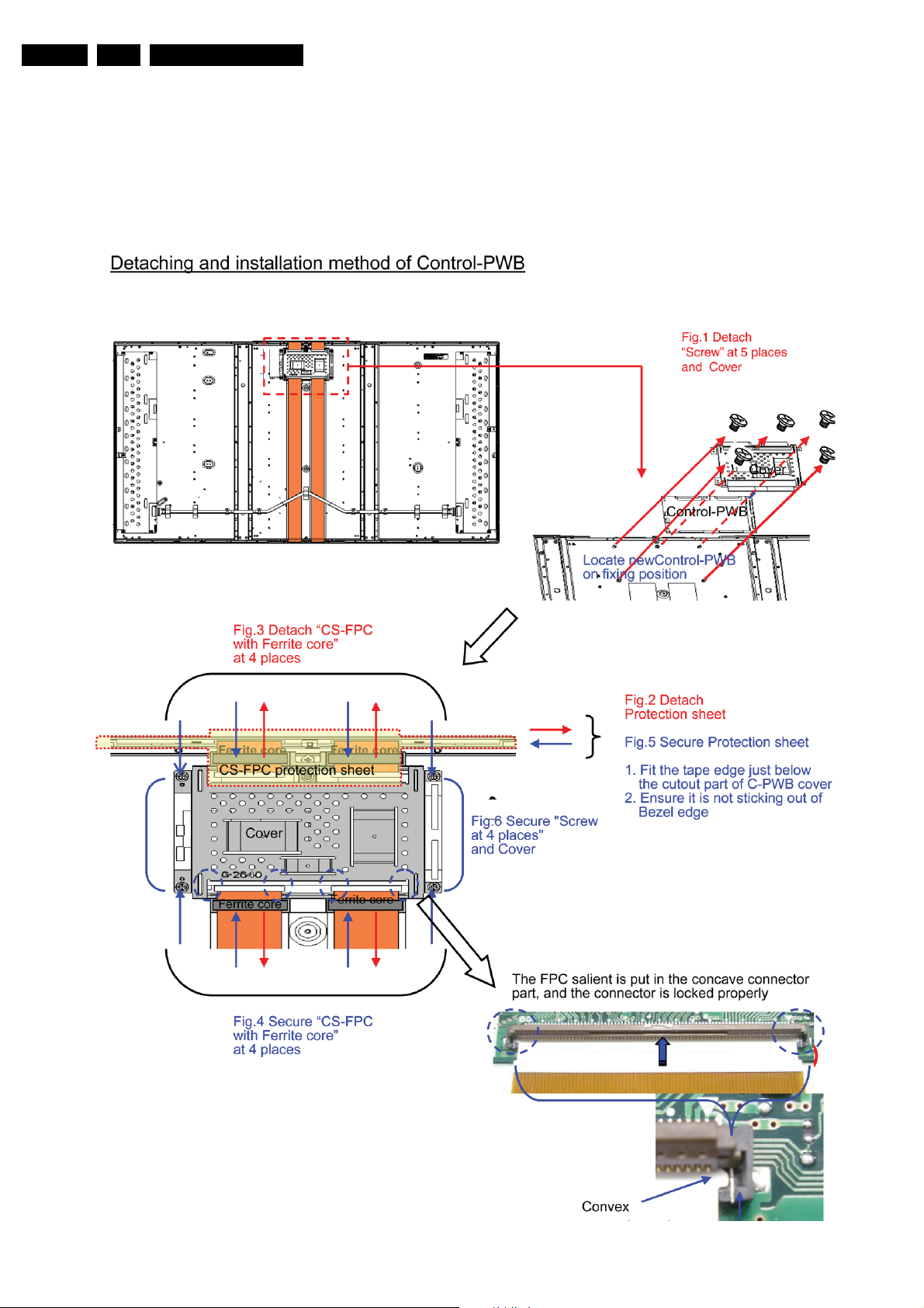
4.13 Model LK520D3LZ9P
4.13.1 Control Board
Mechanical Instructions
Figure 4-22 (Dis)assembly method for the Control Board
Page 29
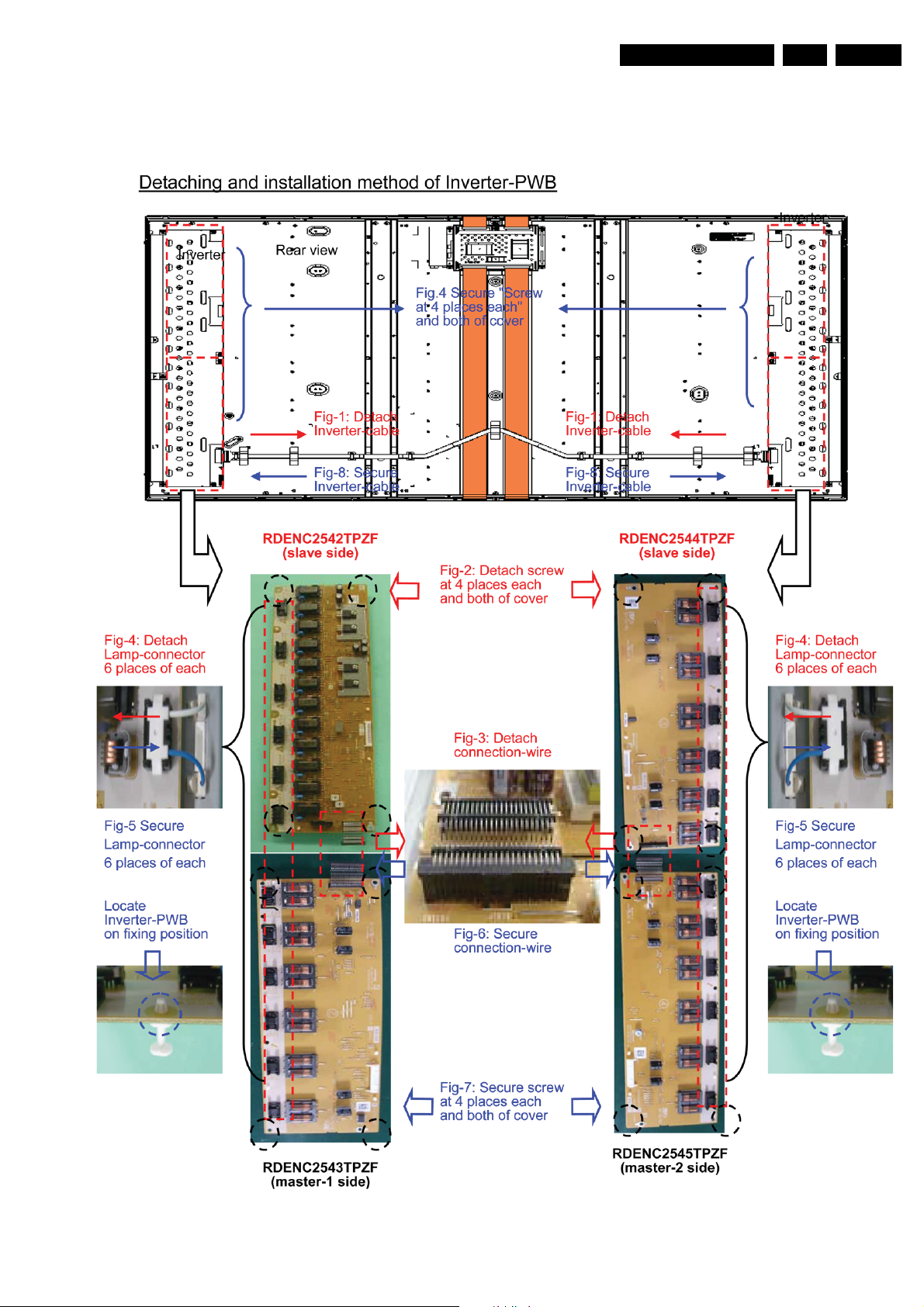
4.13.2 Inverter Board
Mechanical Instructions
EN 29LCD SHARP 2k8 4.
Figure 4-23 (Dis)assembly method for the Inverter Board(s)
I_17812_015.eps
181208
Page 30
EN 30 LCD SHARP 2k85.
y
y
y
g
Service Modes, Error Codes, and Fault Finding
5. Service Modes, Error Codes, and Fault Finding
Index of this chapter:
5.1 Service Modes
5.2 Error Codes
5.3 Fault Finding
5.3.1 General
5.3.2 LK315D3LZ43
5.3.3 LK315D3LZ73
5.3.4 LK315T3LA33
5.3.5 LK315T3LZ53
5.3.6 LK315T3LZ93
5.3.7 LQ315T3LZ23
5.3.8 LK370D3LZ33, LK370D3LZ43, and LK370T3LZ53
5.3.9 LK520D3LZ13 and LK520D3LZ83
5.3.10 LK520D3LZ33 and LK520D3LZ93
5.3.12 LK520D3LZ9P
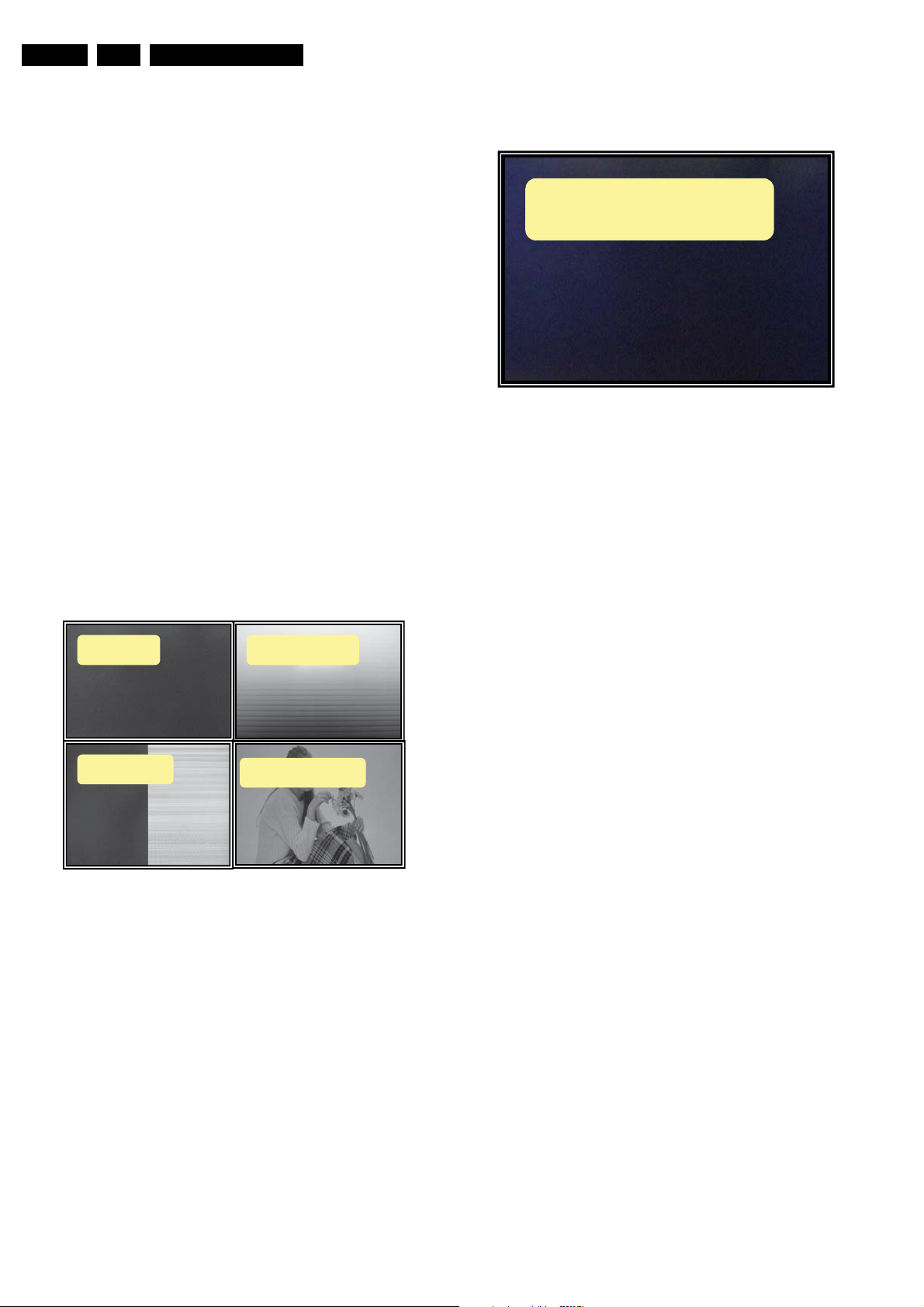
No back light / Flicking
Low bri
htness / Shut down
5.1 Service Modes
Not applicable.
5.2 Error Codes
Not applicable.
5.3 Fault Finding
5.3.1 General
No displa
Half displa
Horizont al strip e
Wavystripedispla
I_17811_027.eps
Figure 5-2 Symptoms for checking the Inverter Board
260908
Figure 5-1 Symptoms for checking the Control Board
I_17811_026.eps
260908
Page 31
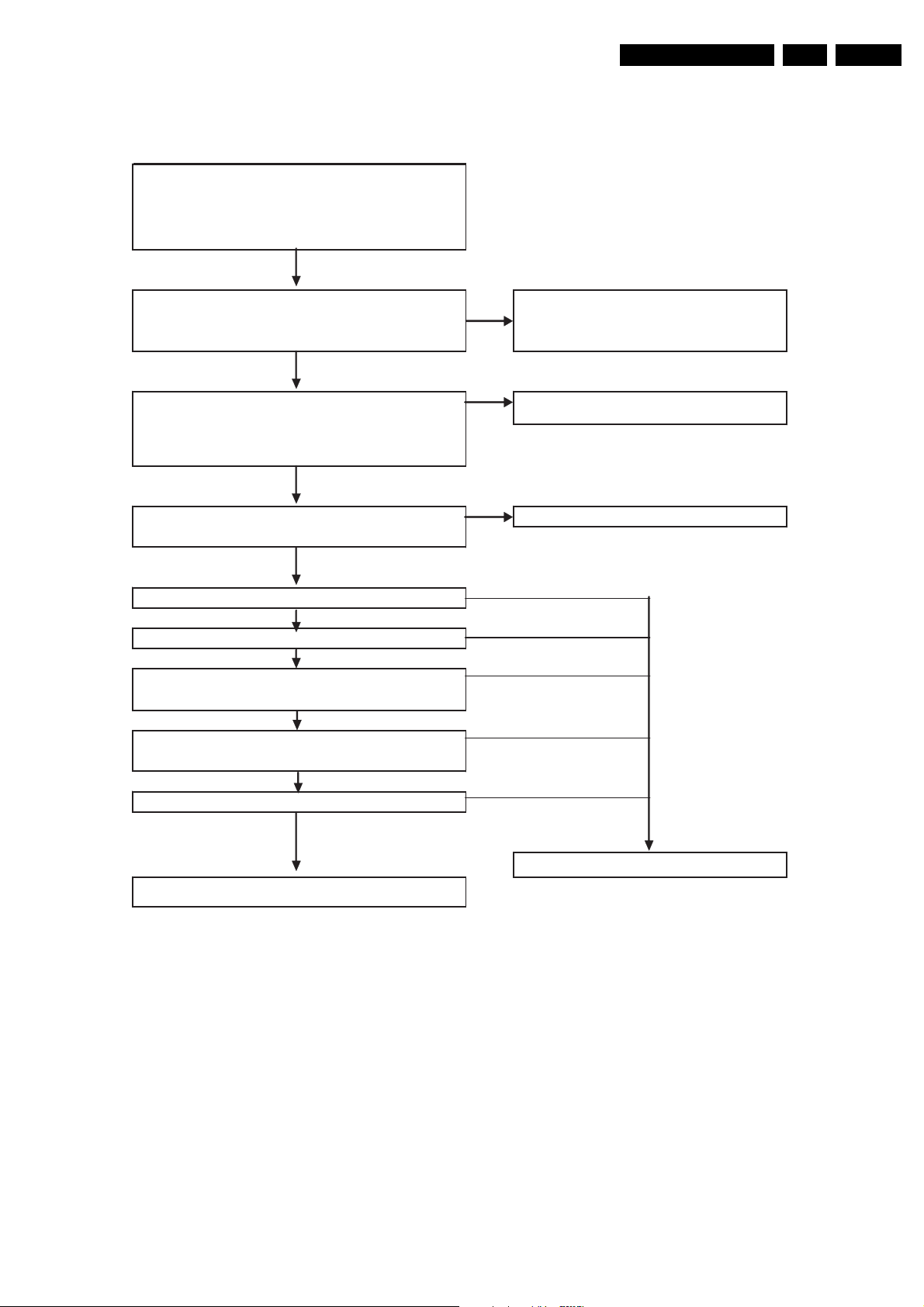
5.3.2 LK315D3LZ43
p
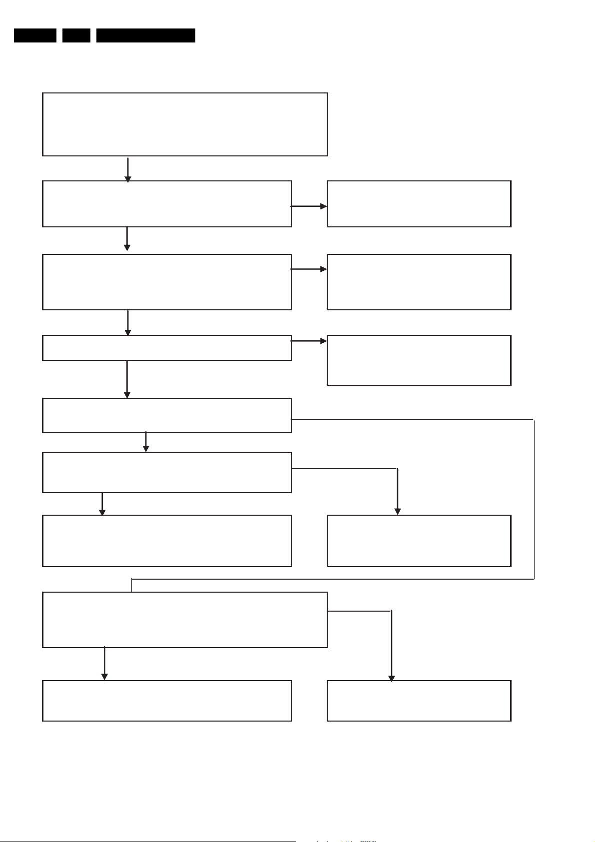
STEP 1
Phenomenon
1. No Display
2. Abnormal Display
(Half Screen Image / Abnormal Display etc.)
ޓޓ
STEP 2
Check cable connection to C-PWB Insert the connector correctly
ޓ1. Cable to LVDS or
ޓ2. FPC between Source-PWB and Contorl-PWB Change the cable and FPC
Service Modes, Error Codes, and Fault Finding
NG
EN 31LCD SHARP 2k8 5.
STEP 3
NG
Check Voltage Check the main board of TV set
Check if pin 1 to 4 (CN2) of Power supply connector
are 12V or not
STEP 4
Check if LVDS si gnal is input to f
ollowing pins or not. Check the main board of TV set
NG
(CN1㧦pins 2-7, 9-14, 16-21, 23-28)
OK
STEP 5
NG
Check if R/ L signal (CN1: pin 31) is "L" or "Open".
Check if U/ D si gnal (CN1: "Open".
pin 32) is "L" or
Check if SELLVDS signal (CN1: pin 30) is "L" or "Open"
Check if TEMP1/2/3 signal (CN1: pins 36,37,38)
NG
NG
NG
is "H" or "Open".
NG
Check if O/ S si gnal (CN1: pin 40) is "H" or "Open".
OK
STEP 6 Check the main board of TV set
Exchange the C-PWB
If failure mode still continue after the exchange of C-
lease return the module to Sharp.
PWB,
Figure 5-3 Trouble shooting table for Control Board
I_17811_014.eps
260908
Page 32
EN 32 LCD SHARP 2k85.
Service Modes, Error Codes, and Fault Finding
STEP 1
The Possible failure Phenomenon would be:
1. No Back Light
2. Flickering
3. Low Bri ghtness
4. Shut down after 3 seconds from switching
STEP2
Check cable connection to Inverter Insert the connector correctly
NG
Cable to 3pin connector and 9pin connector or Change the cable
STEP3
Check Voltage Check the power supply
Check if pin 1 and 3 of connector CN7501
are 60V and 12V.
STEP4
Check if pin 2 of connector CN702 is 3.3V.
OK
NO
(the phenomenon should be #1 of
"STEP1")
OK
NO
Check the main board of TV s
(the phenomenon should be #1 of
OK
"STEP1")
STEP5
Check if pin 7 of connector CN702 is 3.3V
㧜V
Check if pin 3 of connector CN702 is from
0.5V to 3. 3V.
NO
From 0.5V to 3.3V
In case of Phenomenon #3, i t i s
In case of Phenomenon #1, 2, or 4, Inverter
normal.
modul should be returned changed.
et
Check pin 8 of connector CN702.
Brightness should be changed by voltage from 0V to
.3V or not.
3
STEP7
NO
In case of Phenomenon #1, 2, or 4, Inverter
module shoud be returned.
Figure 5-4 Trouble shooting table for Inverter Board
From 0V to 3.3V
In case of Phenomenon #3, i t i
s
normal. (depend on voltage level)
I_17811_015.eps
260908
Page 33
5.3.3 LK315D3LZ73
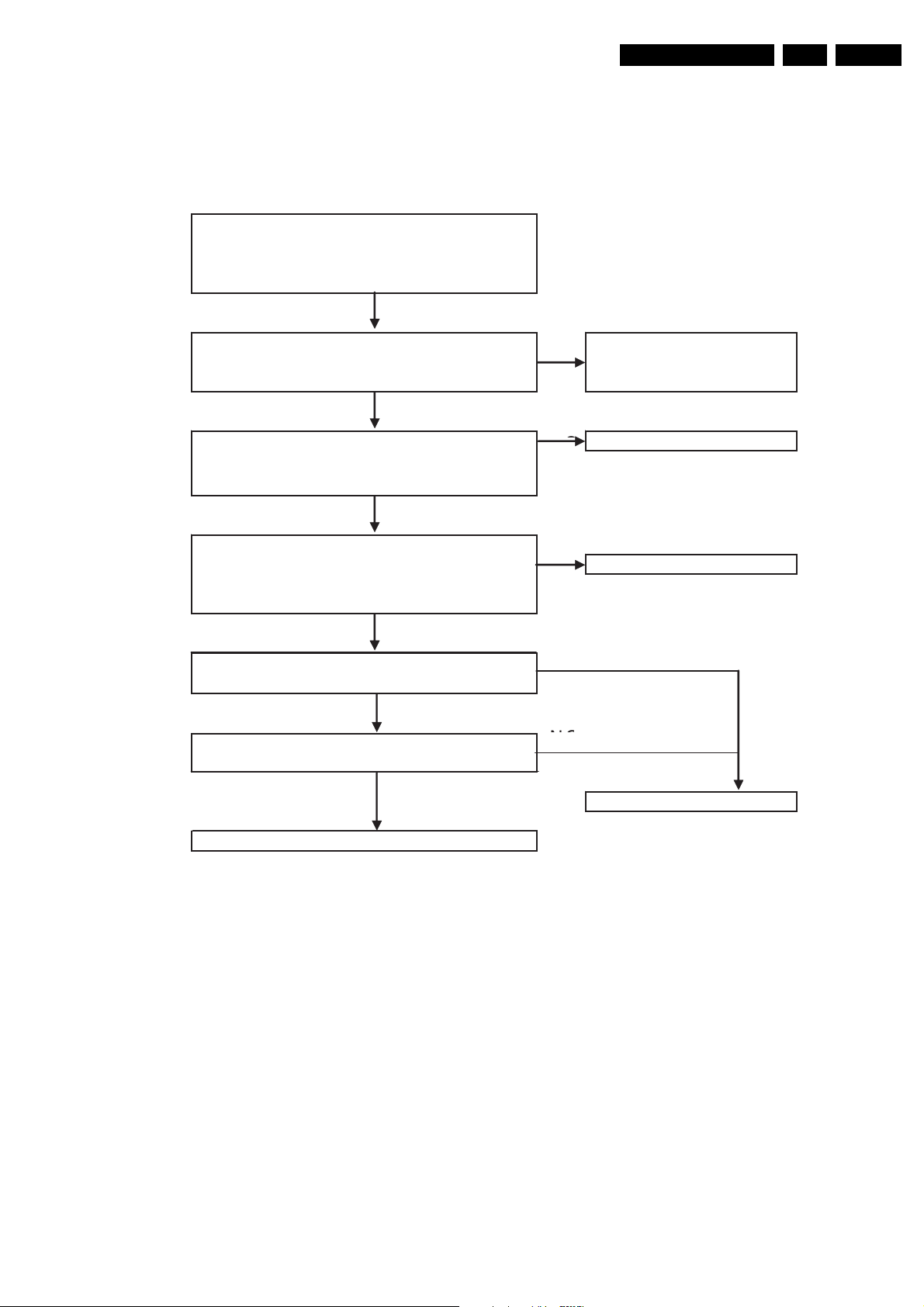
STEP 1
P henomenon
1. N o D isplay
2. A bnormal Display
ޓޓ(H alf screen Image / Abnormal Display etc.)
STEP 2
Check cable connection to C-PWB Insert the connector correctly
ޓ1. Cable to LVDS ro
ޓ2. FPC between Source-PWB and Control-PWB Change the cable and FPC
Service Modes, Error Codes, and Fault Finding
N
EN 33LCD SHARP 2k8 5.
STEP 3
C heck Voltage
C heck if C (N1)47 to 51 pins of LVDS connector are
12V or not
STEP 4
Check if LVDS signal i s input to fo l l o w ing pins or not.
CN1ޓ12-17, 19-20, 22-25, 28-33, 3
CN2ޓ10-15, 17-18, 20-23, 26-31, 33-34, 36-39pin
OK
OK
5-36, 38-41pin
OK
STEP 5
Check if SELLVDS signal (CN1: 7 pin) is “L” or “Open”
not.
Check if 0/S signal (CN1: 6 pin) is “H” or “Open” not.
OK
STEP 6
Exchange the C-PWB
N
Check the main board of the TV set
N
Check the main board of the TV set
NG
NG
C heck the m ain board o f T V set
Note: If failure mode is still seen after exchange
of PWB, please return the module to SHARP
Figure 5-5 Trouble shooting table for Control Board
I_17812_005.eps
031208
Page 34
EN 34 LCD SHARP 2k85.
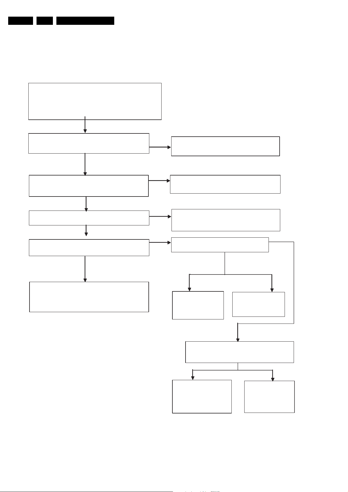
The possible failure phenomenon would be:-
1. No Back Light
2. Flickering
3. Low Brightness
4. Shut down after 3 seconds from switching ON
Service Modes, Error Codes, and Fault Finding
Check cable connection to Inverter
Cable to 14pin connector
㧝㧚
OK
Check Voltage
Check if 1 to 5 pins of 14pin connector are 24V or not.
OK
Check if 12pin of 14pin connector is 3.3V or not
OK
Check if 13pin of 14pin connector is more than 3.3V or not.
OK
3.3V or more
Exchange the Inverter and go to next stage
* If phenomenon #2, 3 or 4 still exists even after
exchange of in
Insert the connector correctly
NG
NO
NO
From 0V to3.3V
or
ޓ
Change the cable
ޓ
Check the power supply
(the phenomenon should be #1 of "STEP1")
Check the main board of TV s et
(the phenomenon should be #1 of "STEP1")
NO
Check if 14pin of 14pin connector is 3.3V or not
In case of Phenomenon
#1, 2, or 4, Inverter
should be changed.
0V:㧦13pin
3.3V
0V
From 0.5V to
3.3V=13pin
In case of Phenomenon
#3, it is normal.
Note: If failure mode is still seen after exchange
of PWB, please return the module to SHARP
Figure 5-6 Trouble shooting table for Inverter Board
Check the voltage of 13pin of 14pin connector
Brightness should be changed by voltage from 0 to
3.3V
In case of Phenomenon
#1, 2, or 4, Inverter should be
changed and go to next
stage
In case of Phenomenon
#3, it is normal. (depend
on voltage level)
I_17812_006.eps
031208
Page 35
5.3.4 LK315T3LA33
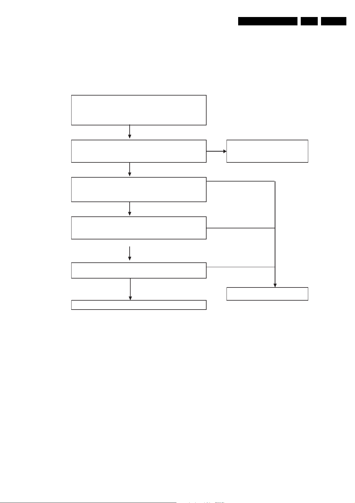
STEP 1
Phenomenon
1. No Display
2. Abnormal Display
ޓޓ
STEP 2
ޓ
2. FPC between Source-PWB and Control-PWB Change the cable and FPC
ޓ
STEP 3
Check Voltage
Check if (CN1) 1 to 4 pins of LVDS connector are 12V or not
Service Modes, Error Codes, and Fault Finding
(Half Screen Image / Abnormal Display etc.)
OK
NG
NG
EN 35LCD SHARP 2k8 5.
yltcerroc rotcennoc eht tresnIBWP-C ot noitcennoc elbac kcehC
roSDVL ot elbaC .1
STEP 4
OK
Check if LVDS signal is input to following pins or not.
CN1 12 -13, 15-16, 18-19, 21-22, 24-25 pin
OK
STEP 5
Check if SELLVDS signal (CN1: 9pin) is “L” or “Open” not.
OK
Exchange the C-PWB
Note: If failure mode is still seen after exchange
of PWB, please return the module to SHARP
NG
NG
aob niam eht kcehC6 PETS
tes VT fo dr
I_17812_010.eps
041208
Figure 5-7 Trouble shooting table for Control Board
Page 36
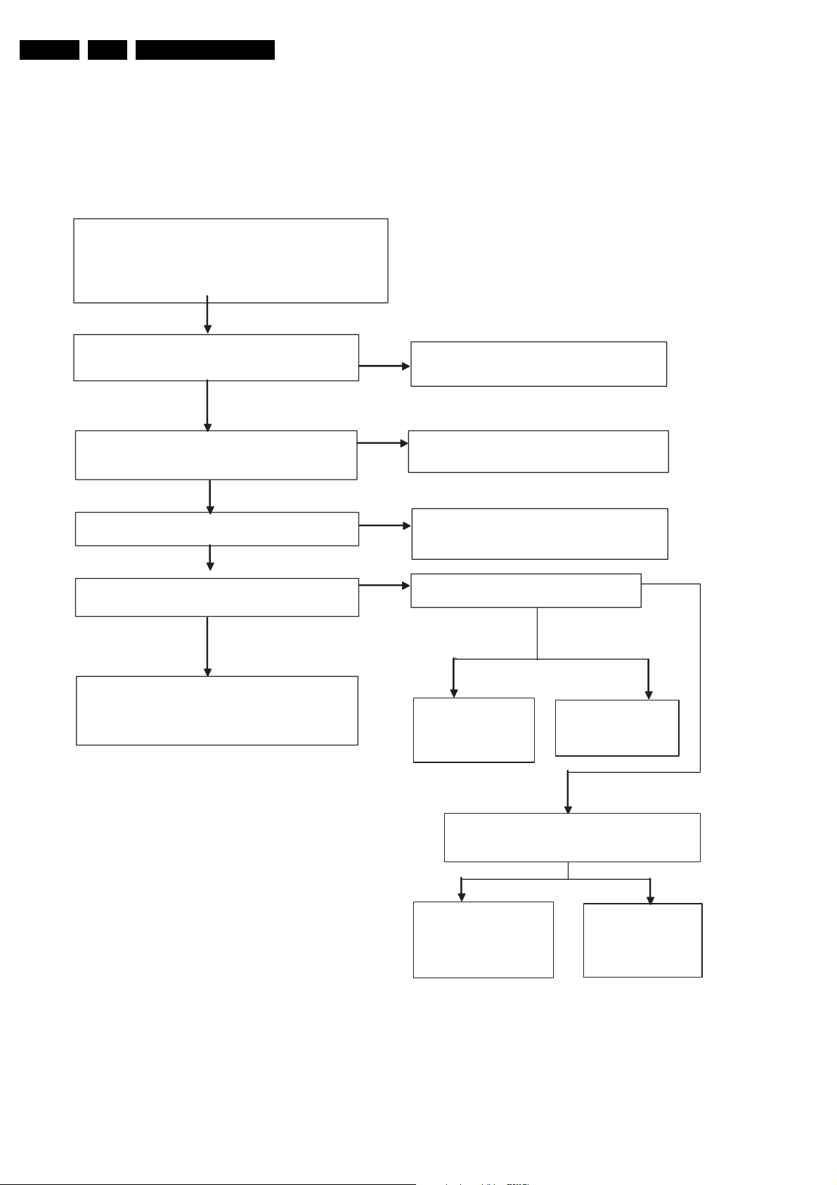
EN 36 LCD SHARP 2k85.
The possible failure phenomenon would be:-
1. No Back Light
2. Flickering
3. Low Brightness
4. Shut down after 3 seconds from switching ON
Service Modes, Error Codes, and Fault Finding
Check cable connection to Inverter
Cable to 14pin connector
㧝㧚
OK
Check Voltage
Check if 1 to 5 pins of 14pin connector are 24V or not.
OK
Check if 12pin of 14pin connector is 3.3V or not
OK
Check if 13pin of 14pin connector is more than 3.3V or not.
OK
3.3V or mo re
Exchange the Inverter and go to next stage
*If phenomenon #2, 3 or 4 still exists even
after exchange of in
Insert the connector correctly
NG
NO
NO
From 0V to3.3V
or
ޓ
Change the cable
ޓ
Check the power supply
(the phenomenon should be #1 of "STEP1")
Check the main board of TV set
(the phenomenon
NO
Check if 14pin of 14pin connector is 3.3V or not
In cas e of Phenomenon
#1, 2, or 4, Inverter
should be changed.
should be #1 of "STEP1")
0V:㧦13pin
3.3V
0V
From 0.5V to
3.3V=1 3pin
In case of Phenomenon
#3, it is normal.
Note: If failure mode is still seen after exchange
of PWB, please return the module to SHARP
Figure 5-8 Trouble shooting table for Inverter Board
Check the voltage of 13pin of 14pin connector
Brightness should be changed by vol tage from 0 to
3.3V
In case of Phenomenon
#1, 2, or 4, Inverter should be
changed and go to next
stage
In case of Phenomenon
#3, it is normal. (depend
on voltage level)
I_17812_011.eps
041208
Page 37
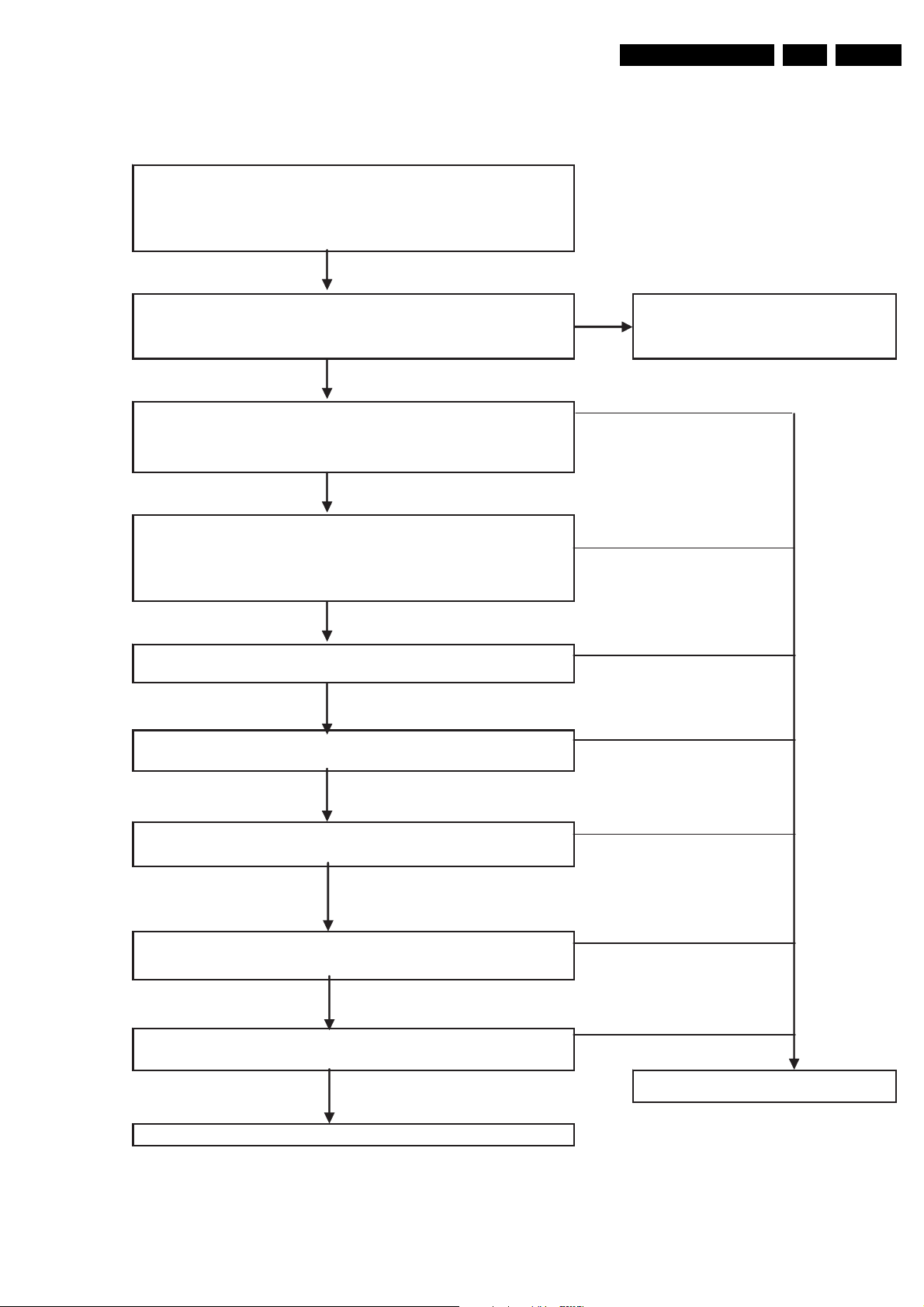
5.3.5 LK315T3LZ53
STEP 1
Phenomenon
1. No Display
2. Abnormal Display
ޓޓ(Half Screen Image / Abnormal Display etc.)
STEP 2
Check cable connection to C-PWB Insert the connector correctly
ޓ1. Cable to LVDS or
ޓ2. FPC between Source-PWB and Contorl-PWB Change the cable and FPC
Service Modes, Error Codes, and Fault Finding
NG
EN 37LCD SHARP 2k8 5.
STEP 3
OK
Check Voltage
Check if 㧔CN1) 1 to 4pins of LVDS connector are 12V or not
OK
STEP 4
Check if LVDS signal is input to following pins or not.
ޓޓޓCN1ޓ12-13, 15-16, 18-19, 21-22,24-25pin
OK
STEP 5
Check if R/L signal(CN1:27pin) is "L" or "Open"not.
Check if U/D signal(CN1:28pin) is "L" or "Open"not.
Check if SELLVDS signal(CN1:9pin) is "L" or "Open" not.
NG
NG
NG
NG
NG
Check if TEMP1/2/3 signal(CN2:4-6pin) is "H" or "Open"not.
Check if O/S signal(CN2:2pin) is "H" or "Open"not.
OK
STEP 6
Exchange the C-PWB
Figure 5-9 Trouble shooting table for Control Board
NG
NG
Check the main board of TV set
I_17811_012.eps
250908
Page 38
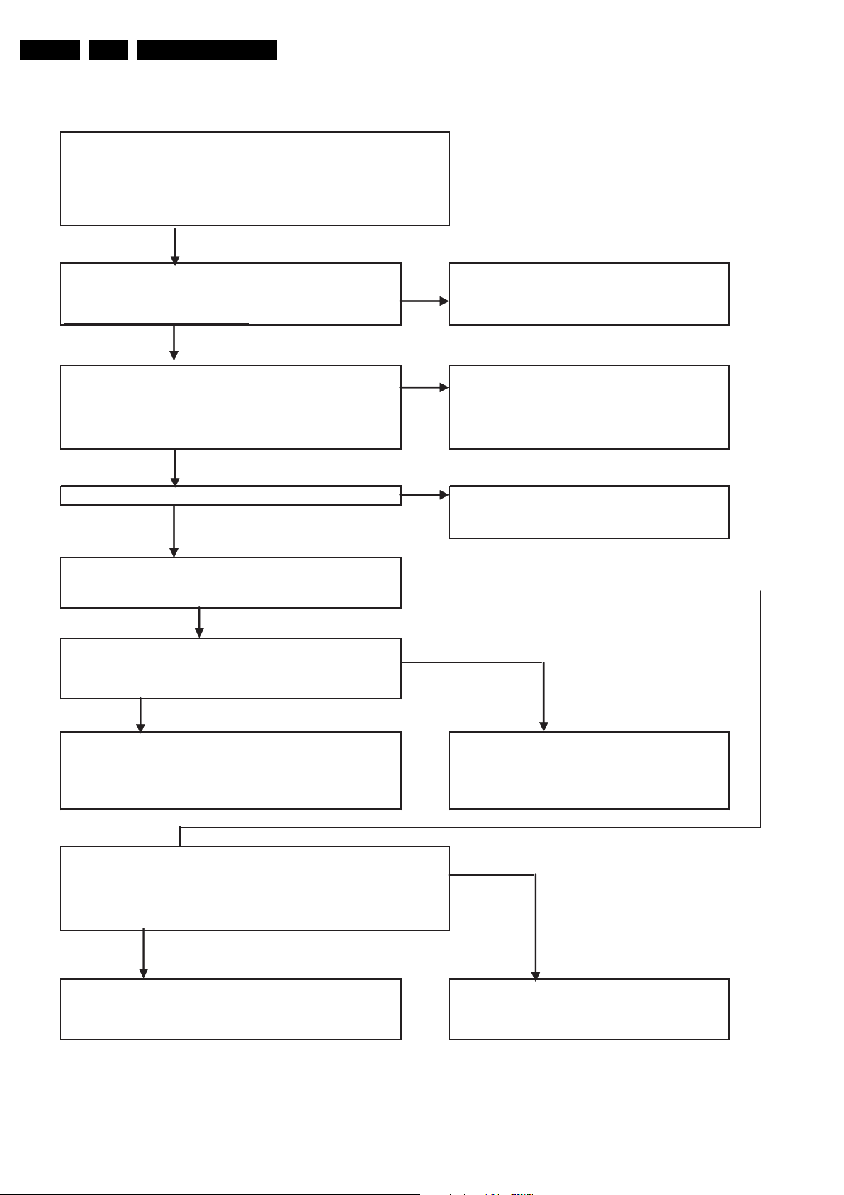
EN 38 LCD SHARP 2k85.
Service Modes, Error Codes, and Fault Finding
STEP 1
The Possible failure Phenomenon would be:
1. No Back Light
2. Flickering
3. Low Brightness
4. Shut down after 3 seconds from switching ON
STEP2
Check cable connection to Inverter Insert the connector correctly
NG
Cable to 3pin connector and 9pin connector or Change the cable
STEP3
Check Voltage Check the power supply
Check if 1pin and 3 pin of 3pin (CN7501)connector are
60V and 12V or not.
STEP4
Check if 2pin of 9pin(CN702) connector is 3.3V or not. Check the main board of TV set
OK
OK
OK
NO
(the phenomenon should be #1 of "STEP1")
NO
(the phenomenon should be #1 of "STEP1")
STEP5
V
Check if 7pin of 9pin connector(CN702) is 3.3V or not.
㧜
Check if 3pin of 9pin(CN702) connector is from 0.5V to
3.3V or not.
From 0.5V to 3.3V
NO
In case of Phenomenon #3, it is normal.
In case of Phenomenon #1, 2, or 4, Inverter modul
should be returned changed.
Check if 8pin of 9pin(CN702) connector.
Brightness should be changed by voltage from 0V to 3.3V or not.
STEP7
NO
In case of Phenomenon #1, 2, or 4, Inverter module
shoud be returned.
Figure 5-10 Trouble shooting table for Inverter Board
From 0V to 3.3V
In case of Phenomenon #3, it is normal.
(depend on voltage level)
I_17811_013.eps
250908
Page 39
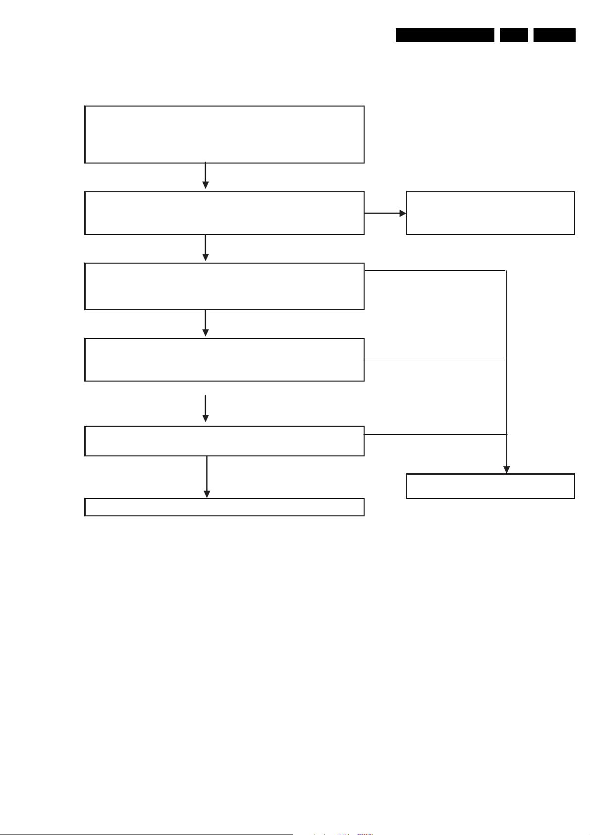
5.3.6 LK315T3LZ93
STEP 1
Phenomenon
1. No Display
2. Abnormal Display
ޓޓ(Half Screen Image / Abnormal Display
STEP 2
Check cable connection to C-PWB Insert the connector correctly
ޓ1. Cable to LVDS or
ޓ2. FPC between Change the cable
Service Modes, Error Codes, and Fault Finding
etc.)
NG
Source-PWB and Contorl-PWB and FPC
EN 39LCD SHARP 2k8 5.
STEP 3
NG
Check Voltage
Check if 㧔CN1) 1 to 4pins of LVDS connector are 12V or not
OK
STEP 4
OK
Check if LVDS signal is input to following pins or not.
NG
ޓޓޓCN1ޓ12-13, 15-16, 18-19, 21-22,24-25pin
OK
STEP 5
Check if SELLVDS signal s "L" or "Open" not.
STEP 6 Check the main board of TV set
(CN1:9pin) i
OK
Exchange the C-PWB
NG
I_17811_010.eps
250908
Figure 5-11 Trouble shooting table for Control Board
Page 40
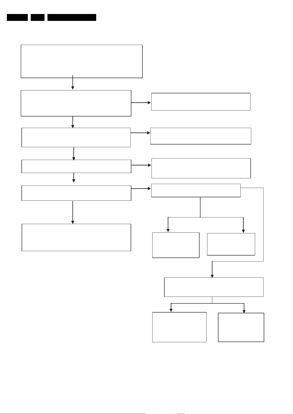
EN 40 LCD SHARP 2k85.
)
STEP 1
The possible failure phenomenon would be:-
1. No Back Light
2. Flickering
3. Low Brightness
4. Shut down after 3 seconds from switching ON
STEP2
Check cable connection to Inverter
㧝㧚Cable to 14pin connector
2㧚Junction Cable between Inverters (in case of 2 sides
inverters)
Service Modes, Error Codes, and Fault Finding
NG
Insert the connector correctly ޓޓor
Change the cable
STEP3
Check Voltage
Check if 1 to 5 pins of 14pin connector are 24V or not.
STEP4
Check if 12pin of 14pin connector is 3.3V or not
STEP5
Check if 13pin of 14pin connector is more than 3.3V
not.
or
STEP6
OK
OK
OK
OK
3.3V or more
Exchange the Inverter and go to next stage
* If phenomenon #2,
or 4 still exi st even
3,
after exchange of in
NO
Check the power supply
(the phenomenon should be #1 of "STEP1")
NO
Check the main board of TV set
(the phenomenon should be #1 of "STEP1")
NO
Check if 14pin of 14pin connector is 3.3V or
not
From 0V to3.3V
In case of
Phenomenon
#1, 2, or 4, Inverter
should be changed.
0V:㧦13pin
3.3V
0V
From 0.5V to
3.3V=13pin
In case of
Phenomenon #3, it is
normal.
Check the voltage of 13pin of 14pin connector
Brightness should be changed by voltage from 0
to 3.3V
In case of Phenomenon
#1, 2, or 4, Inverter should
be changed and go to next
stage
Figure 5-12 Trouble shooting table for Inverter Board
In case of
Phenomenon
#3, it is normal.
(depend on voltage
level
I_17811_011.eps
260908
Page 41
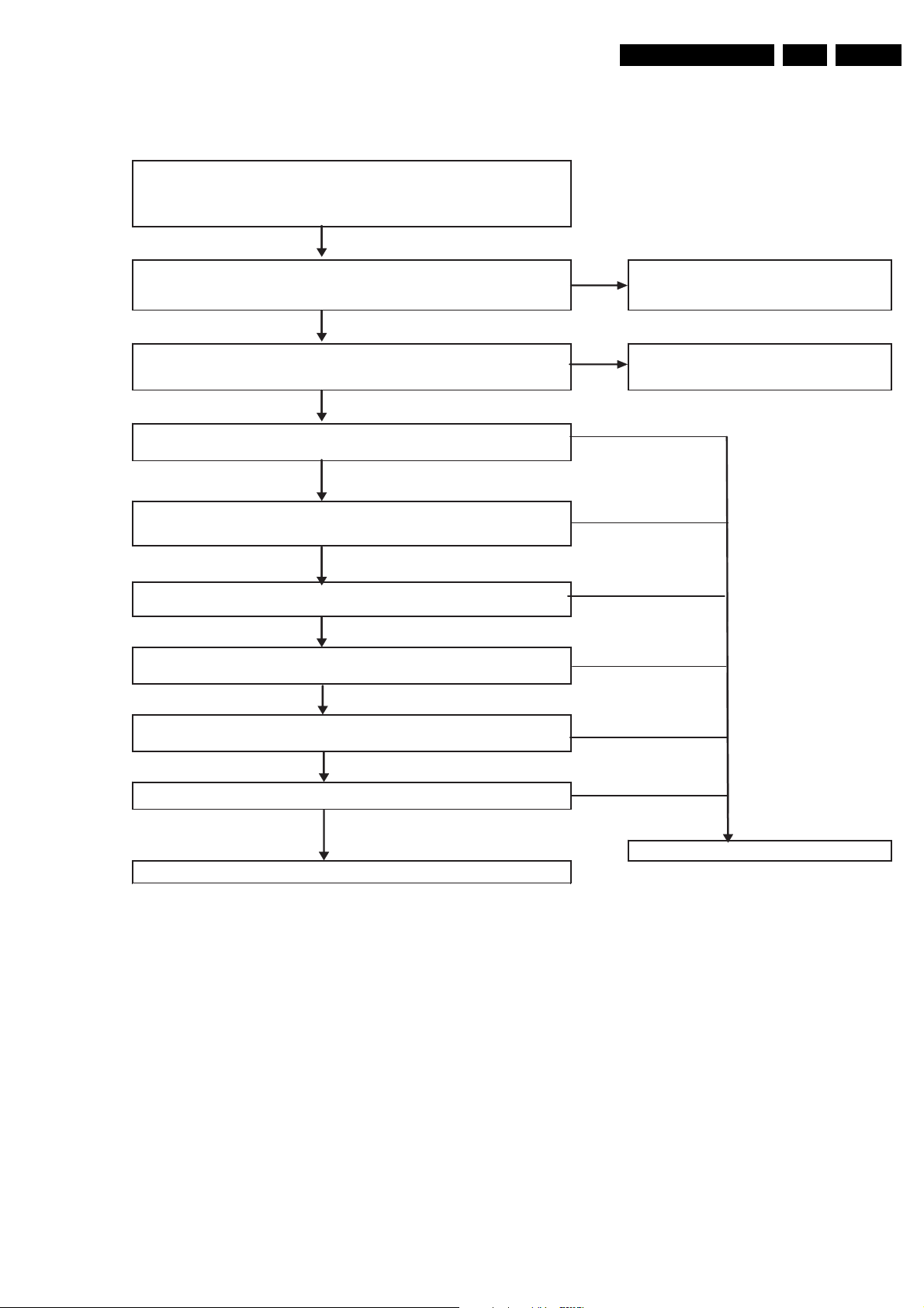
5.3.7 LQ315T3LZ23
STEP 1
Phenomenon
1. No Display
2. Abnormal Display
(Half Scree n Im age / Abnormal Displa y )
ޓޓ
STEP 2
Check cable connection to C-PW B Insert the connector correctly
1. Cable to LVDS or
ޓ
2. FPC between
ޓ
Service Modes, Error Codes, and Fault Finding
etc.
NG
Source-PW B and Contorl-PW B and FPC
Change the cable
EN 41LCD SHARP 2k8 5.
STEP 3
Check Voltage
Check if 1 to 4 pins of LVDS connector are 5V or not
STEP 4
Check if LVDS signal is input to following pins or not.
(CN 1㧦12, 13, 15, 16, 1 8, 1 9, 2 1, 22, 24, 25pin)
STEP 5
Check if R/L signal is "L" or "Open"not.
Check if U/D signal is "L" or "Open"not.
Check if SELLVDS signa is "L" or not.
Check if TEMP1/2/3 signa is "H" or "Open"not.
Check if O/S signal is "H" or "Open"not.
CN1)
㧔
(CN1:27pin)
(CN1:28p in)
l(C N1㧦9pin)
l(C N2㧦4,5,6pin)
(CN2㧦2pin)
NG
Check the main board of TV set
NG
NG
NG
NG
NG
NG
STEP 6 Check the main board of TV set
Exchange the C-PWB
If failure mode still continue after the exchange of C-PW B,
please return the module to Sharp.
I_17811_008.eps
Figure 5-13 Trouble shooting table for Control Board
250908
Page 42
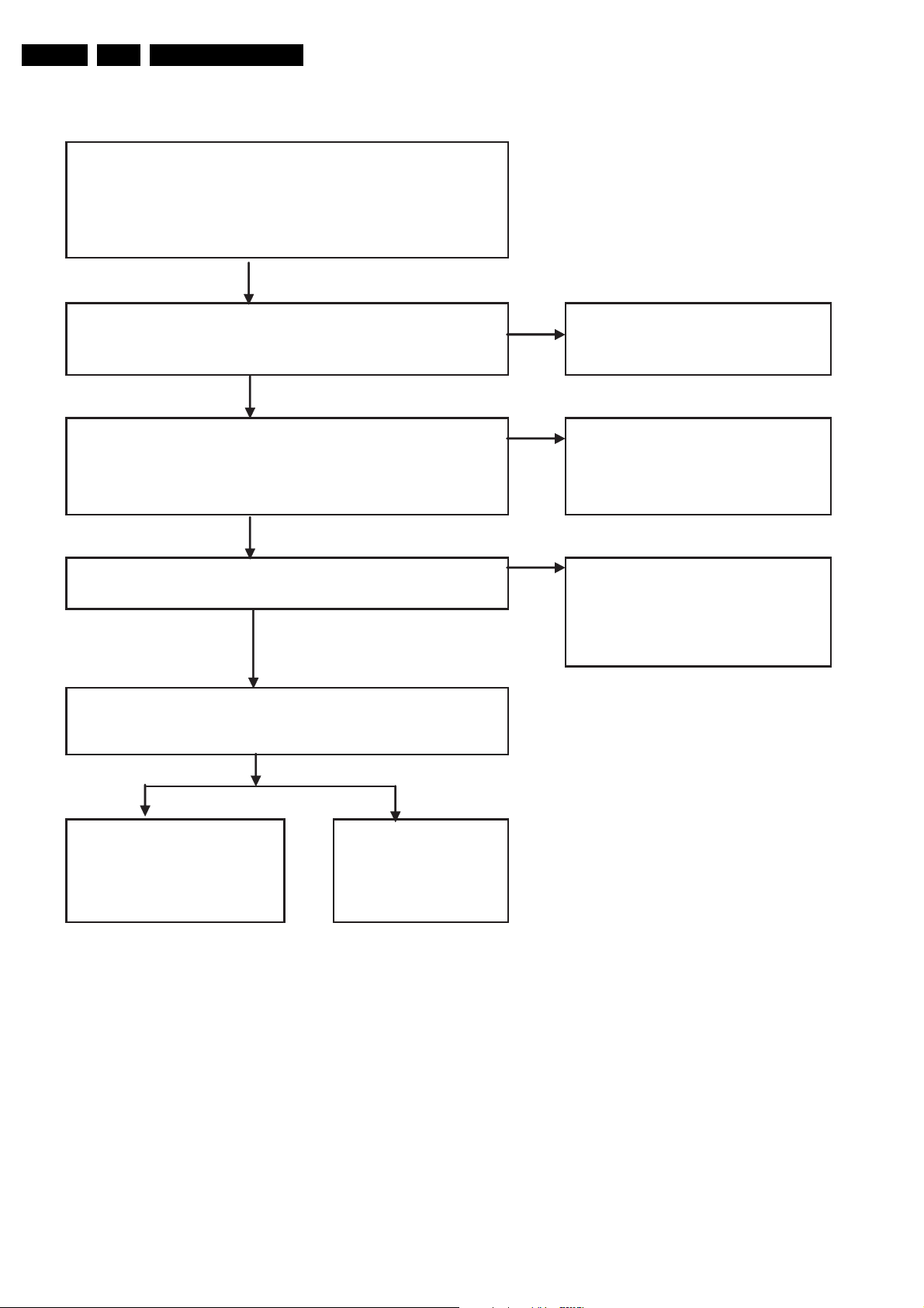
EN 42 LCD SHARP 2k85.
STEP 1
The Possible failure Phenomenon would be:
1. No Back Light
2. Flickering
3. Low Brightness
4. Shut down after 3 seconds from switching ON
STEP2
Check cable connection to Inverter
Service Modes, Error Codes, and Fault Finding
Insert the connector correctly
NG
Cable to 6pin
STEP3
Check Voltage Check the power supply
Check if 1 to 5 pins of 10pin nector are 24V or not.
STEP4
Check if 1pin of 6pin nnector is more then more then
3.3V or not.
(CN3) c (CN4,5) c
onnector and 10 pin onnector
OK
(CN4,5) con
OK
(CN3) co
OK
(3.3V)
or Change the cable
NO
(the phenomenon should be #1 of
"STEP1")
NO
Check the main board of TV set
(0V)
(the phenomenon should be #1 of
"STEP1")
STEP5
Check the voltage of 4pin of 6pin onnector Brightness
(CN3) c
should be changed by voltage from 0V to 5V.
OK
STEP6
Exchange the Inverter In
case of Phenomenon #1, 2, or
4, Inverter should be changed.
In case of Phenomenon
#3, it is normal. (depend
on voltage level)
Figure 5-14 Trouble shooting table for Inverter Board
I_17811_009.eps
260908
Page 43
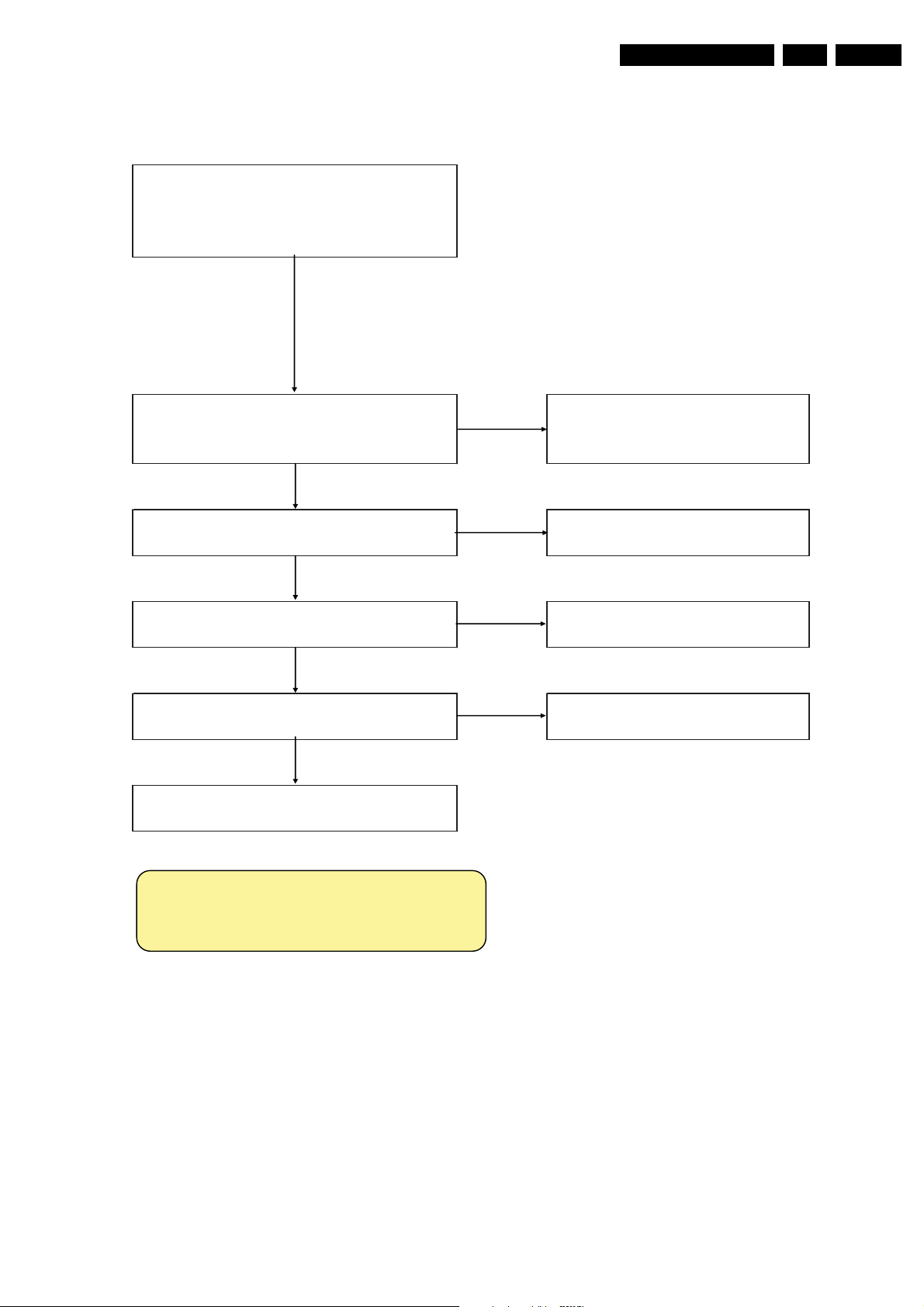
Service Modes, Error Codes, and Fault Finding
5.3.8 LK370D3LZ33, LK370D3LZ43, and LK370T3LZ53
STEP 1
The possible failure phenomenon would be:-
1. No display
2. Abnormal display
(Half display, Abnormal dis play and so on ….. )
STEP 2
Check the connection to Control-PWB
. Cable to LVDS
㪈
2. FPC between Source-PWB and Contorl-PWB
STEP 3
Check Voltage
Please chec k 1 to 4 pins of LV DS connector w ith 12V or not
㪥㪞
㪥㪞
EN 43LCD SHARP 2k8 5.
Insert the connector corre ctly
or
Change the cable and FPC
Check the main board of TV set
STEP 4
Check if LVDS signal is input to following pins or not.
(12 , 13, 15, 16, 18 , 19, 2 1, 22, 24, 25p in)
STEP 5
STEP 6
Exchange the Control-PWB and go to next stage
* Please refer to specifications on the module side
for the location and content of Pin No. described
in this troubleshooting.
㪥㪞
㪥㪞
Check the main board of TV set
Check the main board of TV set Check if SELLVDS signal(9pin) is "L" or not.
I_17810_010.eps
260908
Figure 5-15 Trouble shooting table for Control Board
Page 44
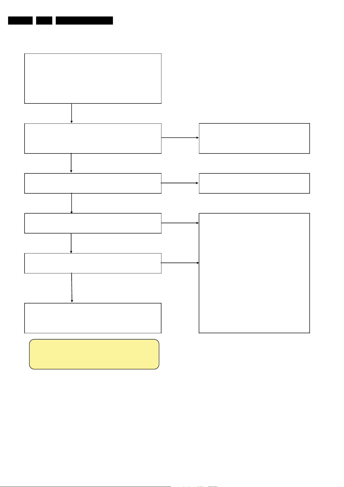
EN 44 LCD SHARP 2k85.
STEP 1
The possible failure phenomenon would be:-
1. No Back Light
2. Flickering
3. Low Brightness
4. Shut down after 3 seconds from switching ON
STEP2
Check cable connection to Inverter
1. Cable to 14pin connector
2. Junction Cable betw een Inverters (in cas e of 2 sides inverters)
Service Modes, Error Codes, and Fault Finding
NG
Insert the connector correctly
or
Change the cable
STEP3
OK
Check Voltage
Check if 1 to 5 pins of 14pin connector are 24V or not.
OK
STEP4
Check if 12pin of 14pin connector is 3.3V or not
OK
STEP5
Check if 13pin of 14pin connector is m ore than 3.3V or not.
OK
STEP6
Exchange the Inverter and go to next stage
* If phenomenon #2, 3, or 4 still exis t even
after exchange of inverter, module should be returned.
NO
NO
NO
Check the power supply
(the phenomenon should be #1 of "STEP1")
Check the main board of TV set
(the phenomenon should be
#1 of "STEP1")
* Please refer to specifications on the module side
for the location and content of Pin No. described
in this troubleshooting.
Figure 5-16 Trouble shooting table for Inverter Board
I_17880_011.eps
260908
Page 45
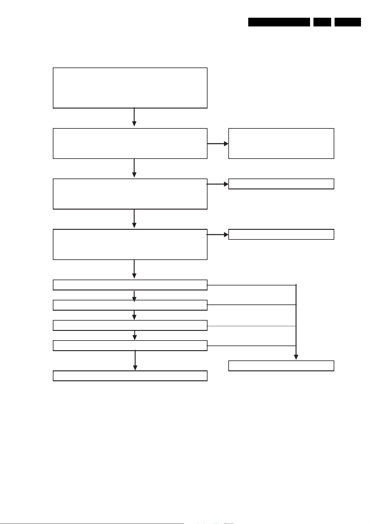
Service Modes, Error Codes, and Fault Finding
5.3.9 LK520D3LZ13 and LK520D3LZ83
STEP 1
Phenomenon
1. No Display
2. Abnormal Display
(Half Screen Image / Abnormal Display
ޓޓ
STEP 2
Check cable connection to C-PWB Insert the connector correctly
1. Cable to LVDS or
ޓ
2. FPC between Change the cable
ޓ
Source-PWB and Contorl-PWB and FPC
STEP 3
Check Voltage Check the main board of TV set
Check if
ޓ
CN1)47 to 51pins of LVDS connector
㧔
are12V or not
EN 45LCD SHARP 2k8 5.
etc.)
NG
OK
NG
STEP 4
Check if LVDS signal is inpu
CN1ޓ12-17, 19-20, 22-25, 28-33, 35-36, 38-39pin
ޓޓ
t to following pins or not. Check the main board of TV set
NG
OK
OK
STEP 5
Check if R/L signal s "L" or "Open"not.
(5pin) i
NG
NG
Check i f U/D signal s "L" or "Open"not.
(6pin) i
NG
Check if SELLVDS signal s "L" or "Open" not.
Check if TEST signas "L" or "Open"not.
(7pin) i
l(㧤pin) i
NG
OK
STEP 6 Check the main board of TV set
Exchange the C-PWB
If failure mode still continue after the exchange of C-PWB,
please return the module to Sharp.
Figure 5-17 Trouble shooting table for Control Board
I_17811_024.eps
260908
Page 46
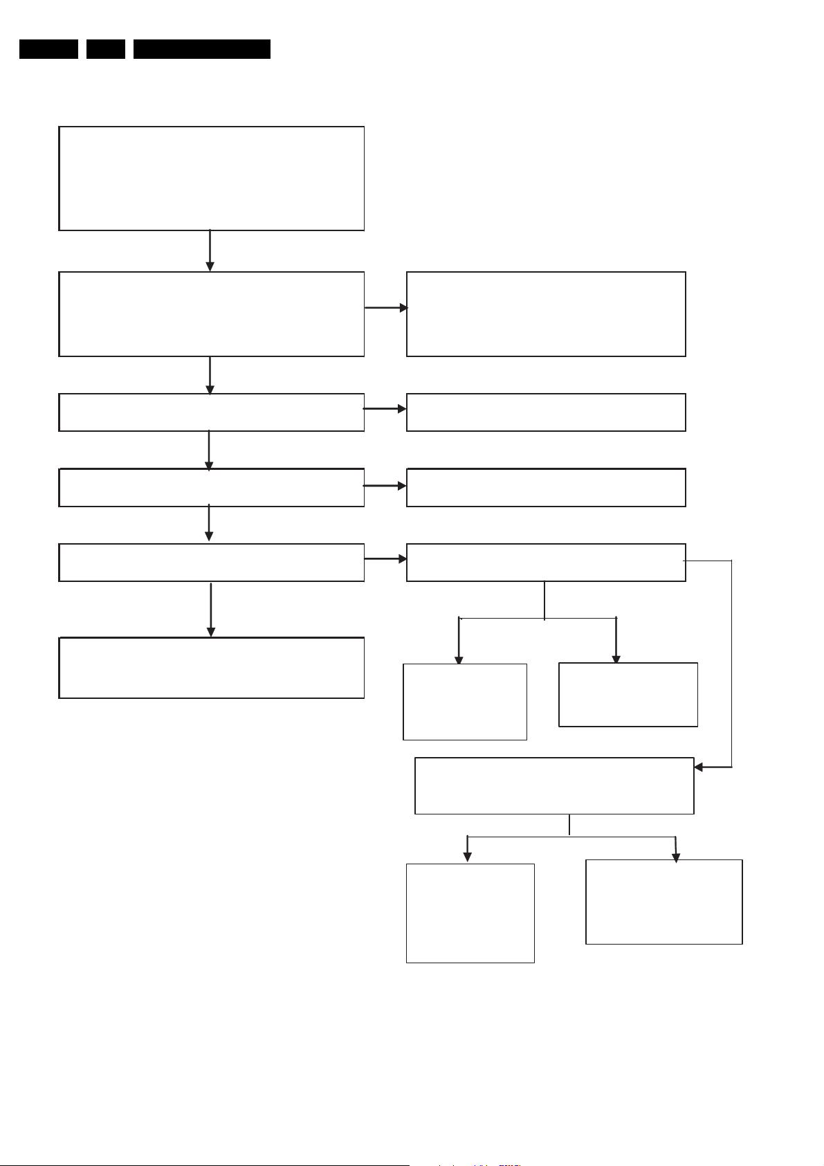
EN 46 LCD SHARP 2k85.
Service Modes, Error Codes, and Fault Finding
STEP 1
The possible failure phenomenon would be:-
1. No Back Light
2. Flickering
3. Low Brightness
4. Shut down after 3 seconds from switching ON
STEP2
Check cable connection to Inverter Insert the connector correctly
NG
1. Cable to 14pin connector or
2. Junction Cable between Inverters (in case of 2
sides inverters)
Change the cable
STEP3
Check Voltage
Check if 1 to 5 pins of 14pin connector are 24V or not.
STEP4
OK
NO
Check the power supply
(the phenomenon should be #1 of "STEP1")
NO
Check if 12pin of 14pin connector is 3.3V or not Check the main board of TV set
(the phenomenon should be #1 of "STEP1")
OK
OK
STEP5
Check if 13pin of 14pin connector is more than 3.3V
or not.
OK
STEP6
3.3V or more
Exchange the Inverter and go to next stage
* If phenomenon #2, 3, or 4 still exist even
after exchange of in
NO
Check if 14pin of 14pin connector is 3.3V or not
From 0V to3.3V
In case of
Phenomenon
#1, 2, or 4, Inverter
0V
0V=13pin
In case of
Phenomenon #3, it is
normal.
should be changed.
Check the voltage of 13pin of 14pin connector
Brightness should be changed by voltage from 0
to 3.3V
3.3V
From 0.5V to
3.3V=13pin
In case of
Phenomenon
#1, 2, or 4, Inverter
should be changed
and go to next stage
Figure 5-18 Trouble shooting table for Inverter Board
In case of Phenomenon
#3, it is normal.
(depend on voltage level)
I_17811_025.eps
260908
Page 47
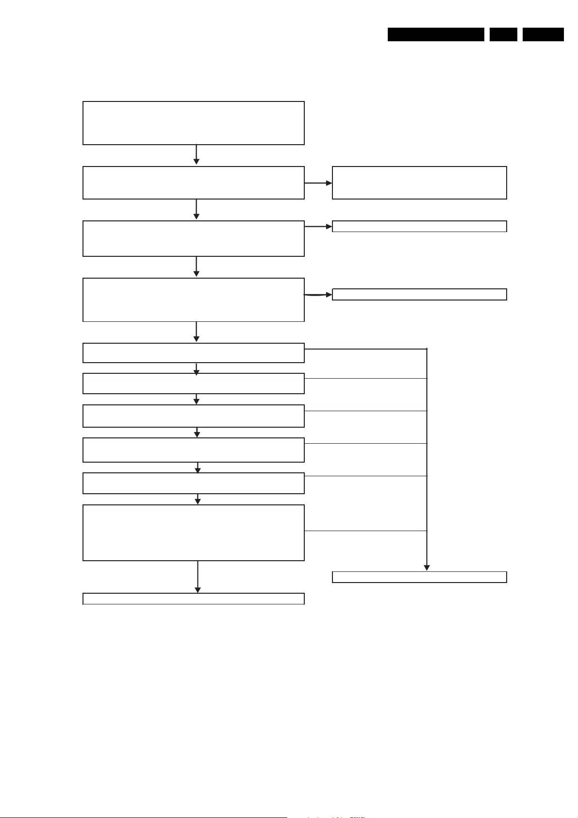
Service Modes, Error Codes, and Fault Finding
5.3.10 LK520D3LZ33 and LK520D3LZ93
STEP 1
Phenomenon
1. No Display
2. Abnormal Display
(Half Screen Image / Abnormal Display
ޓޓ
STEP 2
Check cable connection to C-PWB Insert the connector correctly
1. Cable to LVDS or
ޓ
2. FPC between Change the cable
ޓ
STEP 3
Check Voltage Check the main board of TV set
Check if 㧔CN1)47 to 51pins of LVDS connector are
12V or not
Source-PWB and Contorl-PWB and FPC
OK
EN 47LCD SHARP 2k8 5.
etc.)
N
N
STEP 4
Check if LVDS signal is input to following pins or not.
CN1ޓ12-17, 19-20, 22-25, 28-33, 35-36, 38-41pin Check the main board of TV set
ޓ
ޓCN2ޓ10-15, 17-18, 20-23, 26-31, 33-34, 36-39pin
STEP 5
Check if R/L signal s "L" or "Open".
(CN1:9pin) i
OK
N
OK
NG
NG
Check if U/D signal s "L" or "Open".
Check if SELLVDS signal is "L" or "Open"
Check if TEMP1/2/3 signal s "H" or
"Open".
(CN1:10pin) i
(CN1:7pin)
(CN1:2-4pin) i
NG
NG
NG
Check if O/S signal s "H" or "Open".
Check if BITޓSEL signal ome out from
the TV set.
10BIT㧦"H" or "Open"
8BIT㧦"L"
(CN1:6pin) i
(CN1:8pin) c
NG
STEP 6
Exchange the C-PWB
OK
Figure 5-19 Trouble shooting table for Control Board
Check the main board of TV set
I_17811_022.eps
260908
Page 48
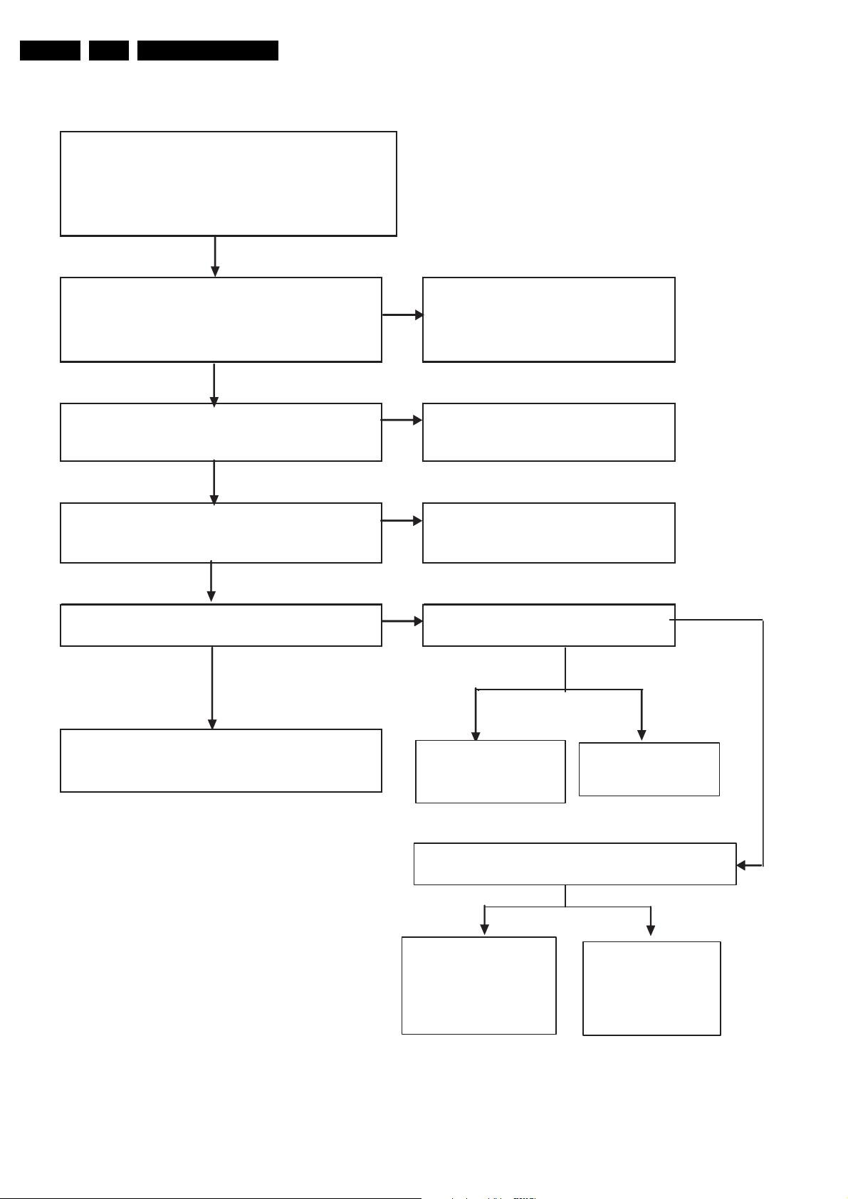
EN 48 LCD SHARP 2k85.
)
)
orma
)
STEP 1
Service Modes, Error Codes, and Fault Finding
The possible failure phenomenon would be:-
1. No Back Light
2. Flickering
3. Low Brightness
4. Shut down after 3 seconds from switching ON
STEP2
Check cable connection to Inverter Insert the connector correctly
1. Cable to 14pin connector or
2. Junction Cable between Inverters (in case of 2
sides inverters)
NG
Change the cable
STEP3
Check Voltage Check the power supply
Check if 1 to 5 pins of 14pin connector are 24V
or not.
STEP4
Check if 12pin of 14pin connector is 3.3V
or not
OK
NO
(the phenomenon should be #1 of
"STEP1"
OK
NO
Check the main board of TV set
(the phenomenon should be #1 of
"STEP1"
STEP5
OK
Check if 13pin of 14pin connector is more than
3.3V or not.
OK
3.3V or more
STEP6
Exchange the Inverter and go to next stage
* If phenomenon #2, 3, or 4 still exist even
after exchange of in
NO
From 0V
to3.3V
Check if 14pin of 14pin connector is
3.3V or not
0V
0V=13pin
In case of Phenomenon
#1, 2, or 4, Inverter
should be changed.
In case of
Phenomenon #3, it is
l.
n
3.3V
From 0.5V to
3.3V=13pin
Check the voltage of 13pin of 14pin connector
Brightness should be changed by voltage from 0 to
In case of Phenomenon
#1, 2, or 4, Inverter
should be changed and
go to next stage
Figure 5-20 Trouble shooting table for Inverter Board
In case of
Phenomenon
#3, it is normal.
(depend on voltage
level
I_17811_023.eps
250908
Page 49
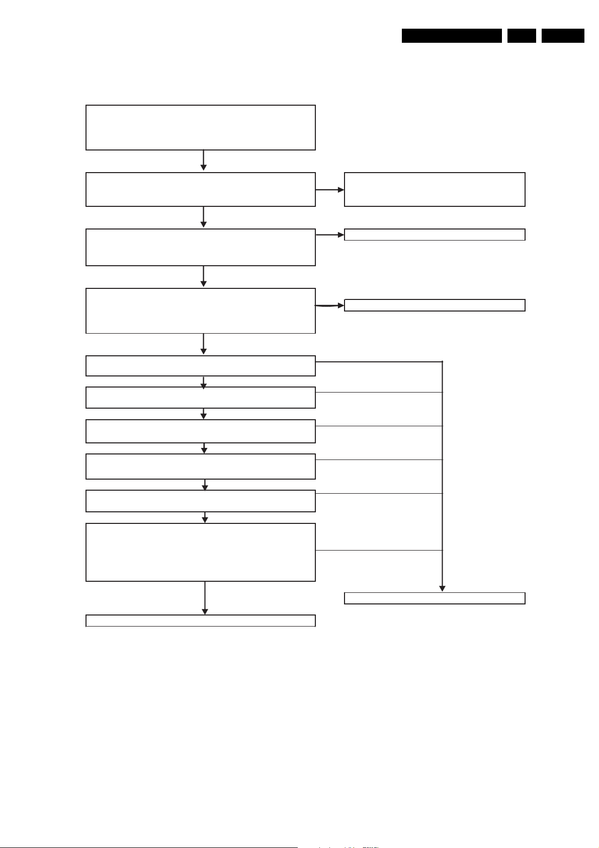
Service Modes, Error Codes, and Fault Finding
5.3.11 LK520D3LZ33 and LK520D3LZ93
STEP 1
Phenomenon
1. No Display
2. Abnormal Display
(Half Screen Image / Abnormal Display
ޓޓ
STEP 2
Check cable connection to C-PWB Insert the connector correctly
1. Cable to LVDS or
ޓ
2. FPC between Change the cable
ޓ
STEP 3
Check Voltage Check the main board of TV set
Check if 㧔CN1)47 to 51pins of LVDS connector are
12V or not
Source-PWB and Contorl-PWB and FPC
OK
EN 49LCD SHARP 2k8 5.
etc.)
N
N
STEP 4
Check if LVDS signal is input to following pins or not.
CN1ޓ12-17, 19-20, 22-25, 28-33, 35-36, 38-41pin Check the main board of TV set
ޓ
ޓCN2ޓ10-15, 17-18, 20-23, 26-31, 33-34, 36-39pin
STEP 5
Check if R/L signal s "L" or "Open".
(CN1:9pin) i
OK
N
OK
NG
NG
Check if U/D signal s "L" or "Open".
Check if SELLVDS signal is "L" or "Open"
Check if TEMP1/2/3 signal s "H" or
"Open".
(CN1:10pin) i
(CN1:7pin)
(CN1:2-4pin) i
NG
NG
NG
Check if O/S signal s "H" or "Open".
Check if BITޓSEL signal ome out from
the TV set.
10BIT㧦"H" or "Open"
8BIT㧦"L"
(CN1:6pin) i
(CN1:8pin) c
NG
STEP 6
Exchange the C-PWB
OK
Figure 5-21 Trouble shooting table for Control Board
Check the main board of TV set
I_17811_022.eps
260908
Page 50
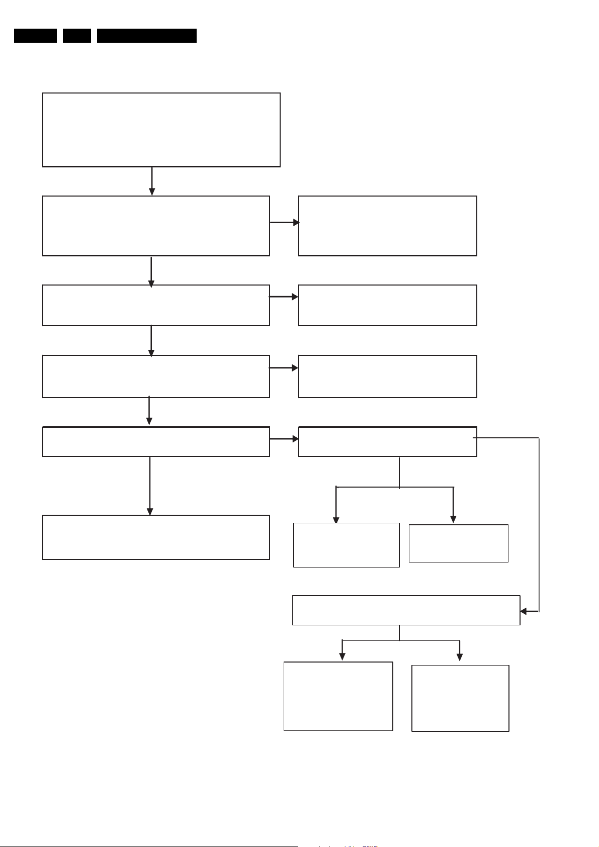
EN 50 LCD SHARP 2k85.
)
)
orma
)
STEP 1
Service Modes, Error Codes, and Fault Finding
The possible failure phenomenon would be:-
1. No Back Light
2. Flickering
3. Low Brightness
4. Shut down after 3 seconds from switching ON
STEP2
Check cable connection to Inverter Insert the connector correctly
1. Cable to 14pin connector or
2. Junction Cable between Inverters (in case of 2
sides inverters)
NG
Change the cable
STEP3
Check Voltage Check the power supply
Check if 1 to 5 pins of 14pin connector are 24V
or not.
STEP4
Check if 12pin of 14pin connector is 3.3V
or not
OK
NO
(the phenomenon should be #1 of
"STEP1"
OK
NO
Check the main board of TV set
(the phenomenon should be #1 of
"STEP1"
STEP5
OK
Check if 13pin of 14pin connector is more than
3.3V or not.
OK
3.3V or more
STEP6
Exchange the Inverter and go to next stage
* If phenomenon #2, 3, or 4 still exist even
after exchange of in
NO
From 0V
to3.3V
Check if 14pin of 14pin connector is
3.3V or not
0V
0V=13pin
In case of Phenomenon
#1, 2, or 4, Inverter
should be changed.
In case of
Phenomenon #3, it is
l.
n
3.3V
From 0.5V to
3.3V=13pin
Check the voltage of 13pin of 14pin connector
Brightness should be changed by voltage from 0 to
In case of Phenomenon
#1, 2, or 4, Inverter
should be changed and
go to next stage
Figure 5-22 Trouble shooting table for Inverter Board
In case of
Phenomenon
#3, it is normal.
(depend on voltage
level
I_17811_023.eps
250908
Page 51
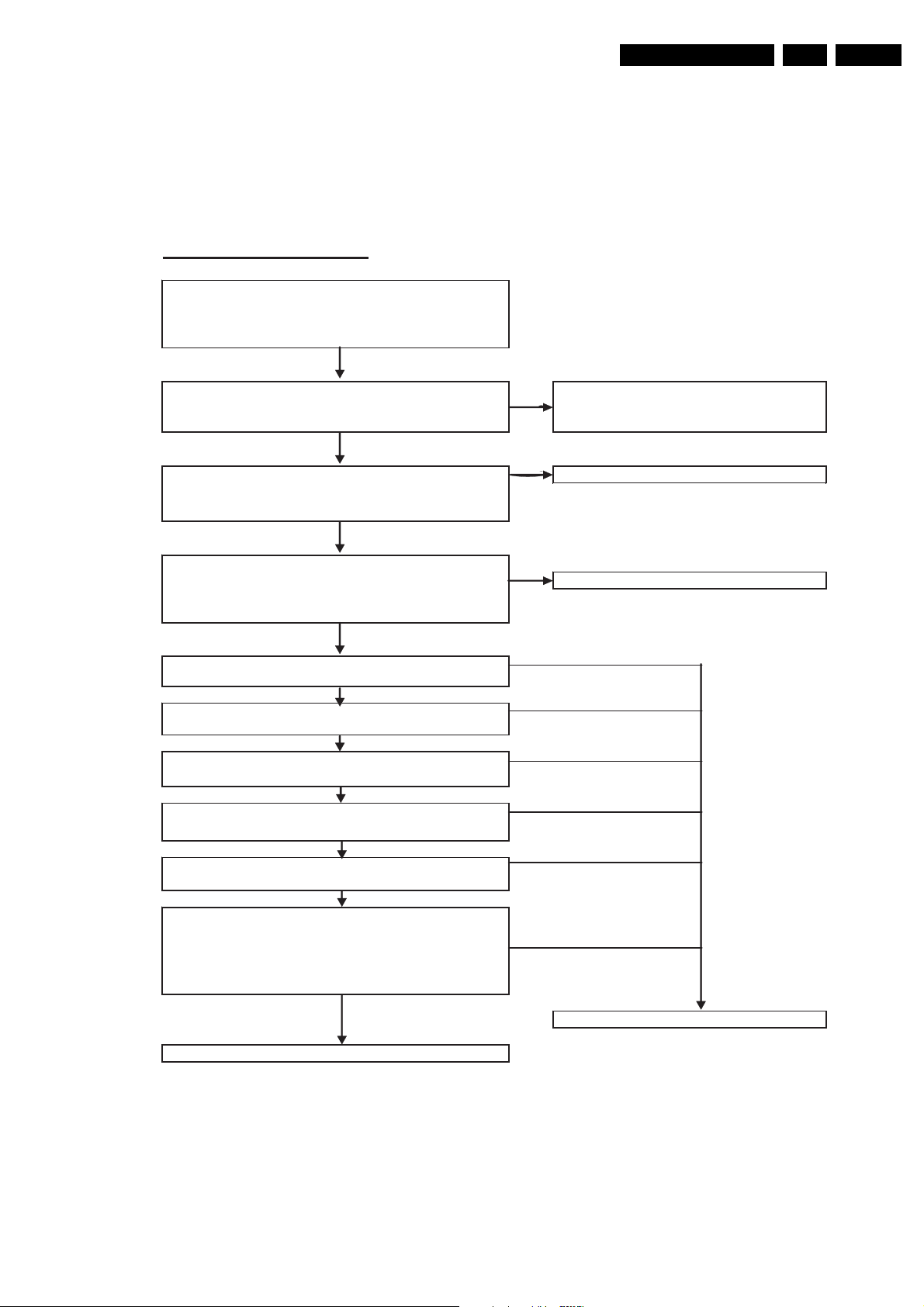
5.3.12 LK520D3LZ9P
Trouble Shooting Table
STEP 1
Phenomenon
1. No Display
2. Abnormal Display
(Half Screen Image / Abnormal Display
䇭䇭
STEP 2
䇭
2. FPC between Change the cable
䇭
STEP 3
Check Voltage Check the main board of TV set
Check if 䋨CN1)47 to 51pins of LVDS connector are
12V or not
Service Modes, Error Codes, and Fault Finding
etc.)
㪥
ro SDVL ot elbaC .1
Source-PWB and Contorl-PWB and FPC
㪦㪢
㪥
EN 51LCD SHARP 2k8 5.
yltcerroc rotcennoc eht tresnI BWP-C ot noitcennoc elbac kcehC
STEP 4
Check if LVDS signal is input to following pins or not.
CN1䇭12-17, 19-20, 22-25, 28-33, 35-36, 38-41pin Check the main board of TV set
䇭
CN2䇭10-15, 17-1 8, 20-23, 26-31, 33-34, 36-39pin
䇭
STEP 5
Check if R/L signal is "L" or "Open"not.
(CN1:9pin)
㪦㪢
㪥
㪦㪢
㪥㪞
㪥㪞
Check if U/D signal s "L" or "Open"not.
Check if SELLVDS signal s "L" or "Open"
not.
Check if TEMP1/2/3 signal "H" or
"Open"not.
(CN1:10pin) i
(CN1:7pin) i
(CN1:2-4pin) is
㪥㪞
㪥㪞
㪥㪞
Check if O/S signal s "H" or "Open"not.
Check if BIT䇭SEL signal me out from
the TV set.
10BIT䋺"H" or "Open"
8BIT䋺"L"
(CN1:6pin) i
(CN1:8pin) co
㪥㪞
STEP 6
Exchange the C-PWB
㪦㪢
Note: If failure mode is still seen after exchange
of PWB, please return the module
Figure 5-23 Trouble shooting table for Control Board
Check the main board of TV set
I_17812_016.eps
181208
Page 52
EN 52 LCD SHARP 2k85.
)
)
)
STEP 1
The possible failure phenomenon would be:-
1. No Back Light
2. Flickering
3. Low Brightness
4. Shut down after 3 seconds from switching ON
STEP2
Check cable connection to Inverter Insert the connector correctly
1. Cable to 14pin connector or
2. Junction Cable between Inverters (in case of 2
sides inverters)
Service Modes, Error Codes, and Fault Finding
Trouble Shooting Table
NG
Change the cable
STEP3
Check Voltage Check the power supply
Check if 1 to 5 pins of 14pin connector are 24V or not.
STEP4
OK
NO
(the phenomenon should be #1 of
"STEP1"
OK
NO
Check if 12pin of 14pin connector is 3.3V or not Check the main board of TV set
(the phenomenon should be #1 of
"STEP1"
STEP5
OK
Check if 13pin of 14pin connector is more than
3.3V or not.
OK
STEP6
㪊㪅㪊㪭㩷㫆㫉㩷㫄㫆㫉㪼
Exchange the Inverter and go to next stage
* If phenomenon #2, 3, or 4 still exist even
after exchange of in
NO
From 0V
to3.3V
Check if 14pin of 14pin connector is
3.3V or not
0V
㪇㪭㪔㪈㪊㫇㫀㫅
In case of Phenomenon
#1, 2, or 4, Inverter
should be changed.
In case of
Phenomenon #3, it is
3.3V
㪝㫉㫆㫄㩷㪇㪅㪌㪭㩷㫋㫆
㪊㪅㪊㪭㪔㪈㪊㫇㫀㫅
Check the voltage of 13pi n of 14pin connector
Brightness should be changed by voltage from 0 to
In case of Phenomenon
#1, 2, or 4, Inverter
should be changed and
Note: If failure mode is still seen after exchange
of PWB, please return the module
Figure 5-24 Trouble shooting table for Inverter Board
go to next stage
In case of
Phenomenon
#3, it is normal.
(depend on voltage
level
I_17812_017.eps
181208
Page 53

Block Diagrams, Test Point Overviews, and Waveforms
6. Block Diagrams, Test Point Overviews, and Waveforms
Not applicable.
7. Circuit Diagrams and PWB Layouts
Not applicable.
8. Alignments
Not applicable.
9. Circuit Descriptions, Abbreviation List, and IC Data Sheets
9.1 Circuit Descriptions
EN 53LCD SHARP 2k8 6.
Not applicable.
9.2 Abbreviation List
AUO Acer Unipack Optronics (supplier)
CCFL Cold Cathode Fluorescent Lamp
CMO Chi Mei Optoelectronics (supplier)
COF Chip On Flex / Foil / Film
CPT Chunghwa Picture Tubes (supplier)
DC Direct Current
FET Field Effect Transistor
FFC Flat Foil Cable
FPC Flexible Printed Circuit
IC Integrated Circuit
9.3 IC Data Sheets
Not applicable.
10. Spare Parts List
For the latest spare part overview, please consult the Philips
Service website.
11. Revision List
Manual xxxx xxx xxxx.0
• First release.
IPB Integrated Power Board (PSU incl.
inverter)
LCD Liquid Crystal Display
LCM Liquid Crystal Module
LED Light Emitting Diode
LPL LG Philips LCD (supplier)
PCB Printed Circuit Board (same as PWB)
PSU Power Supply Unit
PWB Printed Wiring Board (same as PCB)
RGB Red, Green, Blue colour space
TCP Tape Carrier Package
Manual xxxx xxx xxxx.1
• All chapters: LK315D3LZ43, LK315D3LZ53,
LK315D3LZ93, LQ315T3LZ23, LK520D3LZ13,
LK520D3LZ33, and LK520D3LZ83 added.
Manual xxxx xxx xxxx.2
• All chapters: LK315D3LZ73, LK315T3LA33, and
LK520D3LZ9P added.
Page 54

EN 54 LCD SHARP 2k811.
Revision List
 Loading...