

Page 1
Colour Television Chassis
MG8
LC8.1E
LB
MG8
I_18170_000.eps
300708
Contents Page Contents Page
1. Technical Specifications, Connections, and Chassis
Overview 2
2. Safety Instructions, Warnings, and Notes 5
3. Directions for Use 6
4. Mechanical Instructions 7
5. Service Modes, Error Codes, and Fault Finding 12
6. Block Diagrams, Test Point Overview, and
Waveforms
Wiring Diagram 32" (MG8) 23
Wiring Diagram 42" (MG8) 24
Block Diagram Video 25
Block Diagram Audio 26
Block Diagram Control & Clock Signals 27
SSB: Test Points (Overview Bottom Side) 28-30
I2C IC Overview 31
Supply Lines Overview 32
7. Circuit Diagrams and PWB Layouts Diagram PWB
SSB: DC/DC (B01) 33 47-51
SSB: Tuner IF & SAWF (B02) 34 47-51
SSB: Micro Processor NVM (B03) 35 47-51
SSB: TDA154XX (B04A) 36 47-51
SSB: DDR Flash Trap (B04B) 37 47-51
SSB: LVDS Connectors (B04C) 38 47-51
SSB: SMIC L (B05A) 39 47-51
SSB: Audio Class D (B05B) 40 47-51
SSB: YPBPR & SVHS (B06A) 41 47-51
SSB: IO Scart 1 (B06B) 42 47-51
SSB: Scart2 & UART & JTAG (B06C) 43 47-51
SSB: HDMI (B06D) 44 47-51
SSB: SRP List Explanation 45
SSB: SRP List 46
Keyboard Control Panel (E) 52 52
IR & LED Panel (J) 53 54
8. Alignments 55
9. Circuit Descriptions, Abbreviation List, and IC Data
Sheets 58
Abbreviation List 63
IC Data Sheets 65
10. Spare Parts List & CTN Overview 71
11. Revision List 71
©
Copyright 2008 Koninklijke Philips Electronics N.V.
All rights reserved. No part of this publication may be reproduced, stored in a
retrieval system or transmitted, in any form or by any means, electronic,
mechanical, photocopying, or otherwise without the prior permission of Philips.
Published by TY 0872 BU TV Consumer Care Printed in the Netherlands Subject to modification EN 3122 785 18171
Page 2

EN 2 LC8.1E LB1.
Technical Specifications, Connections, and Chassis Overview
1. Technical Specifications, Connections, and Chassis Overview
Index of this chapter:
1.1 Technical Specifications
1.2 Connection Overview
1.3 Chassis Overview
Notes:
• Figures can deviate due to the different set executions.
• Specifications are indicative (subject to change).
1.1 Technical Specifications
1.1.1 Vision
Display type : LCD
Screen size : 32" (82 cm), 16:9
Resolution (HxV pixels) : 1366 × 768
Dyn. contrast ratio : 24000:1
Min. light output (cd/m
Typ. response time (ms) : 6
Viewing angle (HxV degrees) : 176 × 176
Tuning system : PLL
Presets/channels : 99 presets
Tuner bands : VHF, UHF, S, H
TV Colour systems : PAL B/G, D/K, I
Video playback : NTSC
Supported computer formats : 640 × 480
Supported video formats : 480i @ 60 Hz
2
) : 500
: 42" (107 cm), 16:9
: SECAM B/G, D/K, L/L’
: PAL
: SECAM
: 720 × 480
: 800 × 600
: 1024 × 768
: 1280 × 720
: 480p @ 60 Hz
: 576i @ 50 Hz
: 576p @ 50 Hz
: 720p @50, 60 Hz
: 1080i @ 50, 60 Hz
: 1080p @ 24, 25, 30,
50, 60 Hz
1.1.3 Miscellaneous
Power supply:
- Mains voltage (V
- Mains frequency (Hz) : 50 / 60
Ambient conditions:
- Temperature range (°C) : +5 to +35
- Maximum humidity : 90% R.H.
Power consumption (values are indicative)
- Normal operation (W) : ≈ 130 (32")
- Stand-by (W) : < 0.15
Dimensions (W × H × D mm) : 809 × 544 × 92 (32")
Weight incl. packaging (kg) : 18 (32")
) : 220 - 240
AC
: ≈ 200 (42")
: 1033 × 667 × 88 (42")
: 39 (42")
1.1.2 Sound
Sound systems : Nicam Stereo
Maximum power (W
):2 × 10
RMS
Page 3
Technical Specifications, Connections, and Chassis Overview
EN 3LC8.1E LB 1.
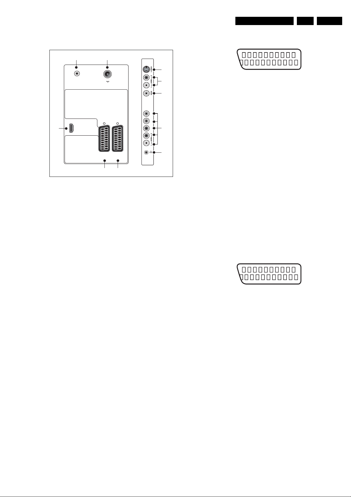
1.2 Connection Overview
12
SERV. U
Ω
75
TV ANTENNA
3
HDMI
EXT 1
EXT 2
(RGB/CVBS)
(CVBS)
4
5
Figure 1-1 Side and rear I/O connections
Note: The following connector colour abbreviations are used
(acc. to DIN/IEC 757): Bk= Black, Bu= Blue, Gn= Green, Gy=
Grey, Rd= Red, Wh= White, and Ye= Yellow.
1.2.1 Connections
1 - Aerial - In
- - IEC-type (EU) Coax, 75 ohm D
6
7
8
YPbPr
9
10
I_18170_027.eps
060808
4 - EXT2: CVBS - In/Out, Audio - In/Out
21
20
E_06532_001.eps
2
1
050404
Figure 1-2 SCART connector
1 -Audio R 0.5 V
2 -Audio R 0.5 V
3 -Audio L 0.5 V
/ 1 kohm k
RMS
/ 10 kohm j
RMS
/ 1 kohm k
RMS
4 -Ground Gnd H
5 -Ground Gnd H
6 -Audio L 0.5 V
/ 10 kohm j
RMS
7-n.c.
8 -Function Select 0 - 2 V: INT
4.5 - 7 V: EXT 16:9
9.5 - 12 V: EXT 4:3 j
9 - Ground Gnd H
10 - n.c.
11 - n.c
12 - n.c.
13 - Ground Gnd H
14 - Ground Gnd H
15 - Video/C 0.7 V
16 - n.c.
/ 75 ohm j
PP
17 - Ground Gnd H
18 - Ground Gnd H
19 - Video CVBS 1 V
20 - Video CVBS 1 V
21 - Shield Gnd H
/ 75 ohm k
PP
/ 75 ohm j
PP
5 - EXT1: Video RGB - In, CVBS - In/Out, Audio - In/Out
2 - Service Connector (UART)
1 -UART_TX Transmit k
2 -Ground Gnd H
3 -UART_RX Receive j
3 - HDMI: Digital Video, Digital Audio - In
1 -D2+ Data channel j
2 -Shield Gnd H
3 -D2- Data channel j
4 -D1+ Data channel j
5 -Shield Gnd H
6 -D1- Data channel j
7 -D0+ Data channel j
8 -Shield Gnd H
9 -D0- Data channel j
10 - CLK+ Data channel j
11 - Shield Gnd H
12 - CLK- Data channel j
13 - CEC Control channel jk
14 - n.c.
15 - DDC_SCL DDC clock j
16 - DDC_SDA DDC data jk
17 - Ground Gnd H
18 - +5V j
19 - HPD Hot Plug Detect j
20 - Ground Gnd H
21
20
E_06532_001.eps
2
1
050404
Figure 1-3 SCART connector
1 - Audio R 0.5 V
2 - Audio R 0.5 V
3 - Audio L 0.5 V
4 - Ground Gnd H
/ 1 kohm k
RMS
/ 10 kohm j
RMS
/ 1 kohm k
RMS
5 - Ground Gnd H
6 - Audio L 0.5 V
7 - Video Blue 0.7 V
8 - Function Select 0 - 2 V: INT
/ 10 kohm j
RMS
/ 75 ohm j
PP
4.5 - 7 V: EXT 16:9
9.5 - 12 V: EXT 4:3 j
9 - Ground Gnd H
10 - n.c.
11 - Video Green 0.7 V
12 - n.c.
/ 75 ohm j
PP
13 - Ground Gnd H
14 - Ground Gnd H
15 - Video Red 0.7 V
/ 75 ohm j
PP
16 - Status/FBL 0 - 0.4 V: INT
1 - 3 V: EXT / 75 ohm j
17 - Ground Gnd H
18 - Ground Gnd H
19 - Video CVBS 1 V
20 - Video CVBS 1 V
/ 75 ohm k
PP
/ 75 ohm j
PP
21 - Shield Gnd H
Page 4
EN 4 LC8.1E LB1.
Technical Specifications, Connections, and Chassis Overview
6 - S-Video (Hosiden): Video Y/C - In
1 - Ground Y Gnd H
2 - Ground C Gnd H
3 - Video Y 1 V
4 - Video C 0.3 V
7, 8 - Cinch: Video CVBS - In, Audio - In
Ye - Video CVBS 1 V
Wh - Audio L 0.5 V
Rd - Audio R 0.5 V
/ 75 ohm j
PP
P / 75 ohm j
PP
/ 75 ohm jq
PP
/ 10 kohm jq
RMS
/ 10 kohm jq
RMS
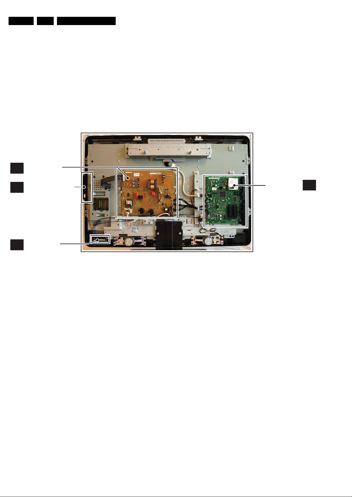
1.3 Chassis Overview
MAIN POWER
A
SUPPLY PANEL
KEYBOARD CONTROL
E
PA NE L
9 - Cinch: Video YPbPr - In, Audio - In
Gn - Video Y 1 V
Bu - Video Pb 0.7 V
Rd - Video Pr 0.7 V
Wh - Audio L 0.5 V
Rd - Audio R 0.5 V
10 - Head phone - Out
Bk - Head phone 32 - 600 ohm / 10 mW rt
/ 75 ohm jq
PP
/ 75 ohm jq
PP
/ 75 ohm jq
PP
/ 10 kohm jq
RMS
/ 10 kohm jq
RMS
SMALL SIGNAL
BOARD
B
IR & LED PANEL
J
Figure 1-4 PWB/CBA locations
I_18170_028.eps
310708
Page 5

Safety Instructions, Warnings, and Notes
2. Safety Instructions, Warnings, and Notes
EN 5LC8.1E LB 2.
Index of this chapter:
2.1 Safety Instructions
2.2 Warnings
2.3 Notes
2.1 Safety Instructions
Safety regulations require the following during a repair:
• Connect the set to the Mains/AC Power via an isolation
transformer (> 800 VA).
• Replace safety components, indicated by the symbol h,
only by components identical to the original ones. Any
other component substitution (other than original type) may
increase risk of fire or electrical shock hazard.
Safety regulations require that after a repair, the set must be
returned in its original condition. Pay in particular attention to
the following points:
• Route the wire trees correctly and fix them with the
mounted cable clamps.
• Check the insulation of the Mains/AC Power lead for
external damage.
• Check the strain relief of the Mains/AC Power cord for
proper function.
• Check the electrical DC resistance between the Mains/AC
Power plug and the secondary side (only for sets that have
a Mains/AC Power isolated power supply):
1. Unplug the Mains/AC Power cord and connect a wire
between the two pins of the Mains/AC Power plug.
2. Set the Mains/AC Power switch to the “on” position
(keep the Mains/AC Power cord unplugged!).
3. Measure the resistance value between the pins of the
Mains/AC Power plug and the metal shielding of the
tuner or the aerial connection on the set. The reading
should be between 4.5 MΩ and 12 MΩ.
4. Switch “off” the set, and remove the wire between the
two pins of the Mains/AC Power plug.
• Check the cabinet for defects, to prevent touching of any
inner parts by the customer.
2.2 Warnings
• All ICs and many other semiconductors are susceptible to
electrostatic discharges (ESD w). Careless handling
during repair can reduce life drastically. Make sure that,
during repair, you are connected with the same potential as
the mass of the set by a wristband with resistance. Keep
components and tools also at this same potential.
• Be careful during measurements in the high voltage
section.
• Never replace modules or other components while the unit
is switched “on”.
• When you align the set, use plastic rather than metal tools.
This will prevent any short circuits and the danger of a
circuit becoming unstable.
2.3 Notes
2.3.1 General
• Measure the voltages and waveforms with regard to the
chassis (= tuner) ground (H), or hot ground (I), depending
on the tested area of circuitry. The voltages and waveforms
shown in the diagrams are indicative. Measure them in the
Service Default Mode (see chapter 5) with a colour bar
signal and stereo sound (L: 3 kHz, R: 1 kHz unless stated
otherwise) and picture carrier at 475.25 MHz for PAL, or
61.25 MHz for NTSC (channel 3).
• Where necessary, measure the waveforms and voltages
with (D) and without (E) aerial signal. Measure the
voltages in the power supply section both in normal
operation (G) and in stand-by (F). These values are
indicated by means of the appropriate symbols.
2.3.2 Schematic Notes
• All resistor values are in ohms, and the value multiplier is
often used to indicate the decimal point location (e.g. 2K2
indicates 2.2 kΩ).
• Resistor values with no multiplier may be indicated with
either an “E” or an “R” (e.g. 220E or 220R indicates 220 Ω).
• All capacitor values are given in micro-farads (μ=× 10
nano-farads (n =× 10
• Capacitor values may also use the value multiplier as the
decimal point indication (e.g. 2p2 indicates 2.2 pF).
• An “asterisk” (*) indicates component usage varies. Refer
to the diversity tables for the correct values.
• The correct component values are listed in the Spare Parts
List. Therefore, always check this list when there is any
doubt.
2.3.3 BGA (Ball Grid Array) ICs
Introduction
For more information on how to handle BGA devices, visit this
URL: www.atyourservice.ce.philips.com (needs subscription,
not available for all regions). After login, select “Magazine”,
then go to “Repair downloads”. Here you will find Information
on how to deal with BGA-ICs.
BGA Temperature Profiles
For BGA-ICs, you must use the correct temperature-profile,
which is coupled to the 12NC. For an overview of these profiles,
visit the website www.atyourservice.ce.philips.com (needs
subscription, but is not available for all regions)
You will find this and more technical information within the
“Magazine”, chapter “Repair downloads”.
For additional questions please contact your local repair help
desk.
2.3.4 Lead-free Soldering
Due to lead-free technology some rules have to be respected
by the workshop during a repair:
• Use only lead-free soldering tin Philips SAC305 with order
code 0622 149 00106. If lead-free solder paste is required,
please contact the manufacturer of your soldering
equipment. In general, use of solder paste within
workshops should be avoided because paste is not easy to
store and to handle.
• Use only adequate solder tools applicable for lead-free
soldering tin. The solder tool must be able:
– To reach a solder-tip temperature of at least 400°C.
– To stabilize the adjusted temperature at the solder-tip.
– To exchange solder-tips for different applications.
• Adjust your solder tool so that a temperature of around
360°C - 380°C is reached and stabilized at the solder joint.
Heating time of the solder-joint should not exceed ~ 4 sec.
Avoid temperatures above 400°C, otherwise wear-out of
tips will increase drastically and flux-fluid will be destroyed.
To avoid wear-out of tips, switch “off” unused equipment or
reduce heat.
• Mix of lead-free soldering tin/parts with leaded soldering
tin/parts is possible but PHILIPS recommends strongly to
avoid mixed regimes. If this cannot be avoided, carefully
clear the solder-joint from old tin and re-solder with new tin.
-9
), or pico-farads (p =× 10
-12
-6
),
).
Page 6

EN 6 LC8.1E LB3.
2.3.5 Alternative BOM identification
It should be noted that on the European Service website,
“Alternative BOM” is referred to as “Design variant”.
The third digit in the serial number (example:
AG2B0335000001) indicates the number of the alternative
B.O.M. (Bill Of Materials) that has been used for producing the
specific TV set. In general, it is possible that the same TV
model on the market is produced with e.g. two different types
of displays, coming from two different suppliers. This will then
result in sets which have the same CTN (Commercial Type
Number; e.g. 28PW9515/12) but which have a different B.O.M.
number.
By looking at the third digit of the serial number, one can
identify which B.O.M. is used for the TV set he is working with.
If the third digit of the serial number contains the number “1”
(example: AG1B033500001), then the TV set has been
manufactured according to B.O.M. number 1. If the third digit is
a “2” (example: AG2B0335000001), then the set has been
produced according to B.O.M. no. 2. This is important for
ordering the correct spare parts!
For the third digit, the numbers 1...9 and the characters A...Z
can be used, so in total: 9 plus 26= 35 different B.O.M.s can be
indicated by the third digit of the serial number.
Identification: The bottom line of a type plate gives a 14-digit
serial number. Digits 1 and 2 refer to the production center (e.g.
AG is Bruges), digit 3 refers to the B.O.M. code, digit 4 refers
to the Service version change code, digits 5 and 6 refer to the
production year, and digits 7 and 8 refer to production week (in
example below it is 2006 week 17). The 6 last digits contain the
serial number.
Directions for Use
MODEL :
PROD.NO:
2.3.6 Board Level Repair (BLR) or Component Level Repair (CLR)
If a board is defective, consult your repair procedure to decide
if the board has to be exchanged or if it should be repaired on
component level.
If your repair procedure says the board should be exchanged
completely, do not solder on the defective board. Otherwise, it
cannot be returned to the O.E.M. supplier for back charging!
2.3.7 Practical Service Precautions
• It makes sense to avoid exposure to electrical shock.
• Always respect voltages. While some may not be
32PF9968/10
AG 1A0617 000001
Figure 2-1 Serial number (example)
While some sources are expected to have a possible
dangerous impact, others of quite high potential are of
limited current and are sometimes held in less regard.
dangerous in themselves, they can cause unexpected
reactions that are best avoided. Before reaching into a
powered TV set, it is best to test the high voltage insulation.
It is easy to do, and is a good service precaution.
MADE IN BELGIUM
220-240V 50/60Hz
~
VHF+S+H+UHF
BJ3.0E LA
S
E_06532_024.eps
128W
260308
3. Directions for Use
You can download this information from the following websites:
http://www.philips.com/support
http://www.p4c.philips.com
Page 7

4. Mechanical Instructions
Index of this chapter:
4.1 Cable Dressing
4.2 Service Positions
4.3 Assy/Panel Removal MG8 Styling
4.4 Set Re-assembly
Notes:
• Figures below can deviate slightly from the actual situation,
due to the different set executions.
4.1 Cable Dressing
Mechanical Instructions
EN 7LC8.1E LB 4.
Figure 4-1 Cable dressing 32" sets
I_18170_029.eps
310708
Page 8
EN 8 LC8.1E LB4.
Mechanical Instructions
4.2 Service Positions
For easy servicing of this set, there are a few possibilities
created:
• The buffers from the packaging (see figure “Rear cover”).
• Foam bars (created for Service).
4.2.1 Foam Bars
1
Required for sets
1
42"
Figure 4-2 Cable dressing 42" sets
The foam bars (order code 3122 785 90580 for two pieces) can
be used for all types and sizes of Flat TVs. See figure “Foam
bars” for details. Sets with a display of 42" and larger, require
four foam bars [1]. Ensure that the foam bars are always
supporting the cabinet and never only the display.
Caution: Failure to follow these guidelines can seriously
damage the display!
By laying the TV face down on the (ESD protective) foam bars,
a stable situation is created to perform measurements and
alignments. By placing a mirror under the TV, you can monitor
the screen.
I_18170_030.eps
300708
E_06532_018.eps
Figure 4-3 Foam bars
171106
Page 9
Mechanical Instructions
EN 9LC8.1E LB 4.
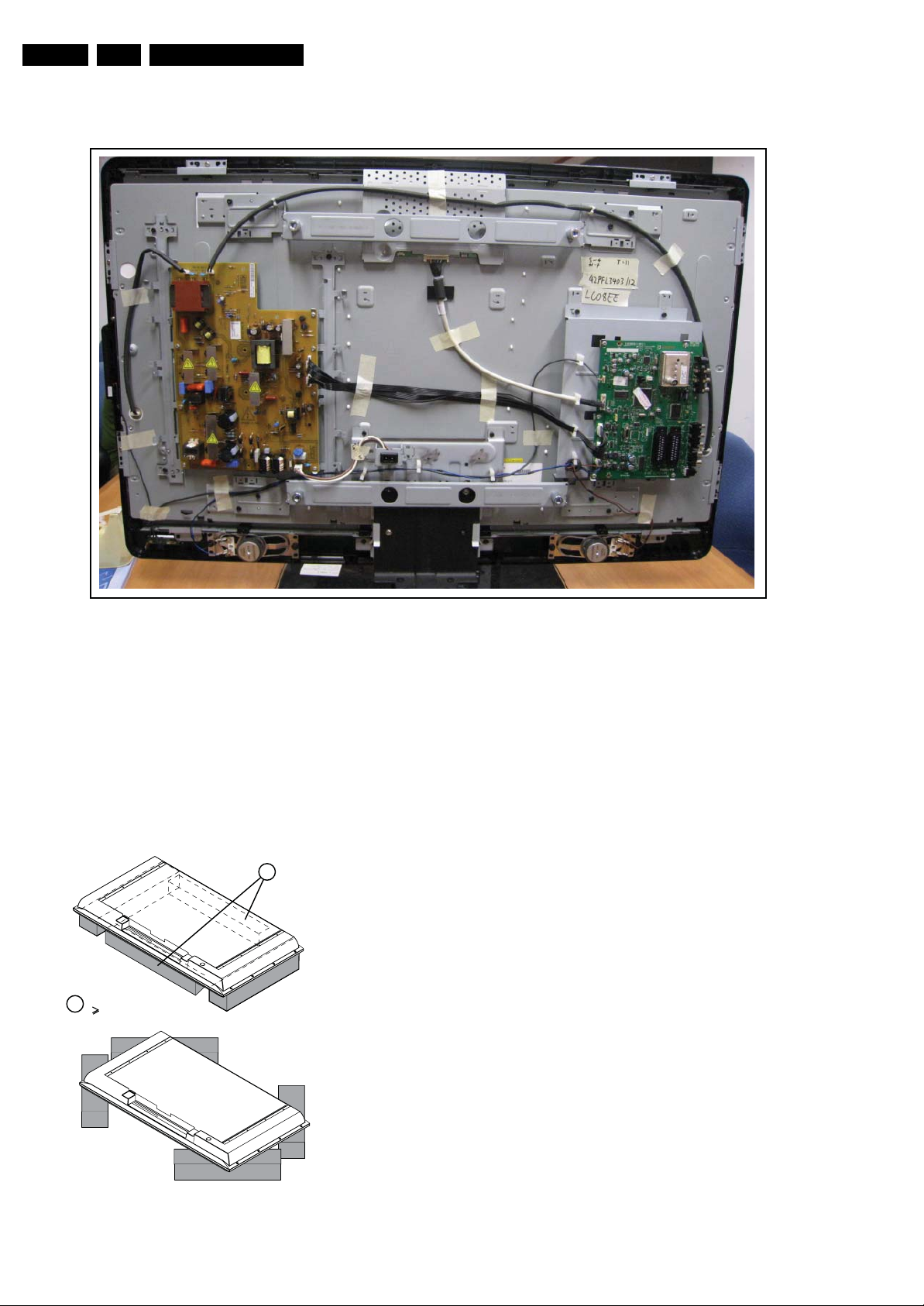
4.3 Assy/Panel Removal MG8 Styling
Pictures are taken from 32” set.
4.3.1 Rear Cover
Warning: Disconnect the mains power cord before you remove
the rear cover.
You can remove the backcover without removing the stand.
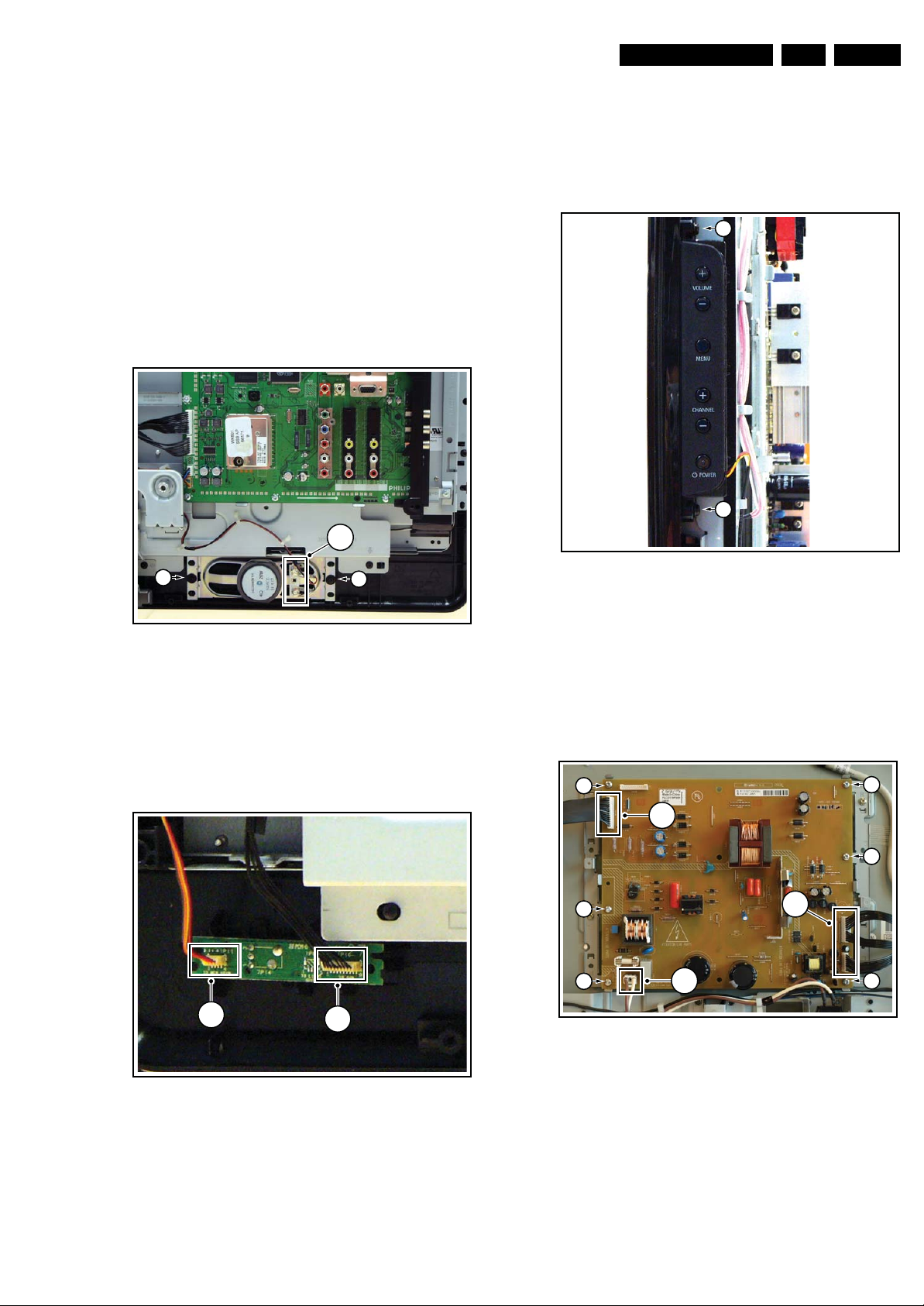
4.3.2 Speakers
Refer to next figure for details.
1. Unplug the connectors [1].
2. Remove the screws [2] and lift the speaker from the back
cover.
1
(
2x
)
2
2
I_17911_001.eps
300608
4.3.4 Keyboard Control Panel
Refer to next figure for details.
1. Unplug the key board connector from the IR & LED board.
2. Remove the screws [1].
3. Lift the unit and take it out of the set.
When defective, replace the whole unit.
1
1
Figure 4-6 Key Board
4.3.5 Main Power Supply Panel 32"
I_17911_003.eps
300608
Figure 4-4 Speakers
4.3.3 IR & LED Panel
Refer to next figure for details.
1. Unplug connectors [1].
2. Release the clips and take the panel out.
When defective, replace the whole unit.
1
Refer to next figure for details.
1. Unplug connectors [1].
2. Remove the fixation screws [2].
3. Take the board out.
When defective, replace the whole unit.
2
2
1
2
1
2x
)
2
2
1
1
(
2
I_18170_050.eps
310708
Figure 4-7 Main Power Supply Panel 32"
I_17911_002.eps
300608
Figure 4-5 IR & LED Board
Page 10

EN 10 LC8.1E LB4.
4.3.6 Small Signal Board (SSB)
Mechanical Instructions
Refer to next figure for details.
Caution: it is mandatory to remount all different screws at their
original position during re-assembly. Failure to do so may result
in damaging the SSB.
1. Unplug the LVDS connector [1].
Caution: be careful, as this is a very fragile connector!
2. Unplug the connectors [2].
3. Remove the screws [3].
4. The SSB can now be taken out of the set, together with the
side cover.
5. To remove the side cover, push back the clamp [4] using a
screw driver.
6. Pull the cover sidewards from the SSB.
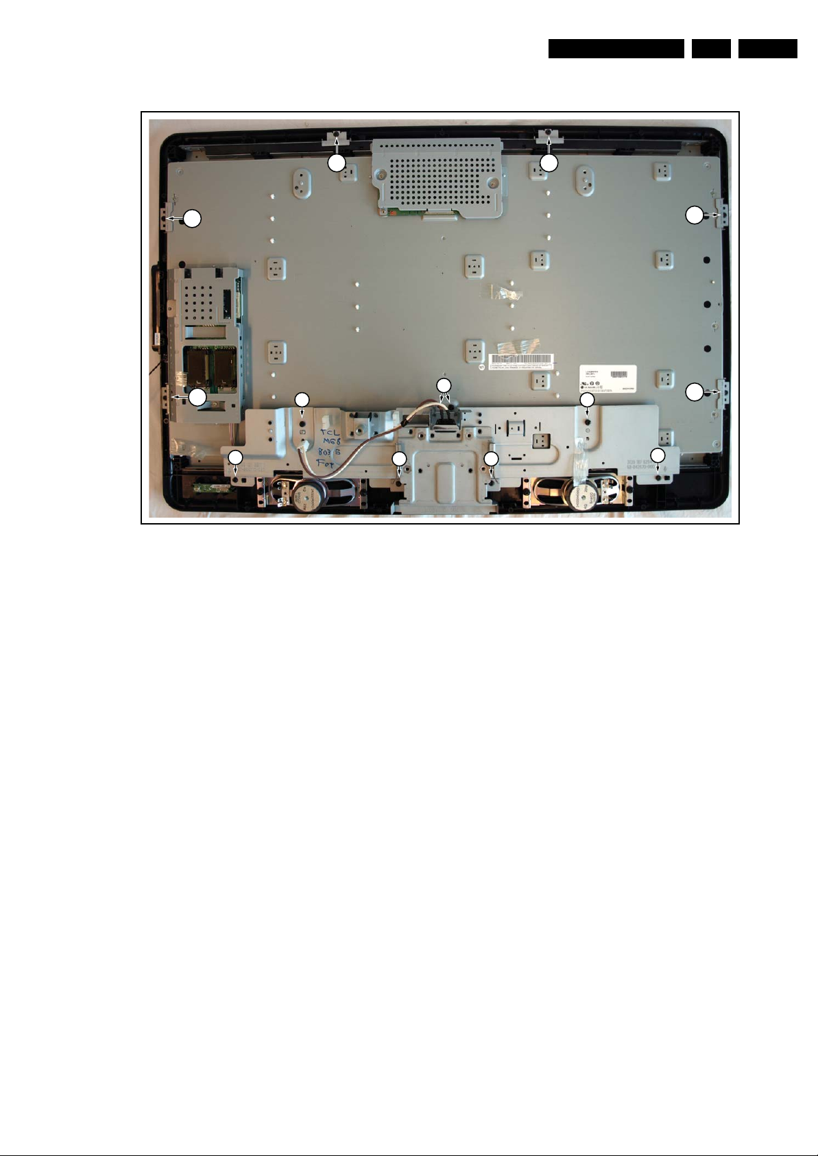
4.3.7 LCD Panel
Refer to next figures for details.
1. Remove the stand [1].
2. Unplug the LVDS connector [2].
3. Unplug connectors [3] from
– Main Power Supply Panel
– Speakers
– IR & LED Panel.
4. Remove any adhesive tape [4] that prevents cables being
removed from the set.
5. Remove all cables from clamps [5] that prevents them from
being removed from the set.
3
3
2
1
3
2
(
3x
)
3
4
3
I_18170_051.eps
310708
Figure 4-8 Small Signal Board
6. Remove the VESA stand [6].
7. Remove the Main Power Supply Panel together with it’s
subframe [7].
8. Remove the Small Signal Board together with it’s
subframe [8].
9. Remove the subframe that holds the stand [9].
10. Remove the clamps that secure the LCD Panel [10] and
take the panel out.
6
6
2
8
7
7
8
4
3
7
3
2x)
(
7
4
3
8 8
4
3
5
1 1
4
11
3
3
I_18170_052.eps
310708
Figure 4-9 LCD Panel -1-
Page 11
Mechanical Instructions
EN 11LC8.1E LB 4.
1010
10
10
4.4 Set Re-assembly
10
9
9 9
9
Figure 4-10 LCD Panel -2-
99
9
I_18170_053.eps
10
310708
To re-assemble the whole set, execute all processes in reverse
order.
Notes:
• While re-assembling, make sure that all cables are placed
and connected in their original position. See figure “Cable
dressing”.
• Pay special attention not to damage the EMC foams on the
SSB shields. Ensure that EMC foams are mounted
correctly.
Page 12
EN 12 LC8.1E LB5.
Service Modes, Error Codes, and Fault Finding
5. Service Modes, Error Codes, and Fault Finding
Index of this chapter:
5.1 Test Points
5.2 Service Modes
5.3 Service Tools
5.4 Error Codes
5.5 The Blinking LED Procedure
5.6 Software Upgrading
5.7 Fault Finding and Repair Tips
5.1 Test Points
In the chassis schematics and layout overviews, the test points
(Fxxx) are mentioned. In the schematics, test points are
indicated with a rectangular box around “Fxxx” or “Ixxx”, in the
layout overviews with a “half-moon” sign.
As most signals are digital, it will be difficult to measure
waveforms with a standard oscilloscope. Several key ICs are
capable of generating test patterns, which can be controlled via
ComPair. In this way it is possible to determine which part is
defective.
5.2 Service Modes
The Service Mode feature is split into four parts:
• Simplified Service Default Mode (SDM).
• Service Alignment Mode (SAM).
• Customer Service Mode (CSM).
• Computer Aided Repair Mode (ComPair).
SDM and SAM offer features, which can be used by the Service
engineer to repair/align a TV set. Some features are:
• Activates the blinking LED procedure for error identification
when no picture is available (SDM).
• Make alignments (e.g. white tone), (de)select options,
enter options codes, reset the error buffer (SAM).
• Display information (“SAM” indication in upper right corner
of screen, error buffer, software version, options and option
codes, sub menus).
The CSM is a Service Mode that can be enabled by the
consumer. The CSM displays diagnosis information, which the
customer can forward to the dealer or call centre. In CSM
mode, “CSM”, is displayed in the top right corner of the screen.
The information provided in CSM and the purpose of CSM is to:
• Increase the home repair hit rate.
• Decrease the number of nuisance calls.
• Solved customers' problem without home visit.
• B is the region indication: E= Europe, A= AP/China,
U=NAFTA, L= LATAM.
• C is the display indication: L= LCD, P= Plasma.
• D is the language/feature indication: 1= standard, H=1080p
full HD.
• X is the main version number: this is updated with a major
change of specification (incompatible with the previous
software version). Numbering will go from 1 - 9 and A - Z.
– If the main version number changes, the new version
number is written in the NVM.
– If the main version number changes, the default
settings are loaded.
• YY is the sub version number: this is updated with a minor
change (backwards compatible with the previous versions)
Numbering will go from 00 - 99.
– If the sub version number changes, the new version
number is written in the NVM.
– If the NVM is fresh, the software identification, version,
and cluster will be written to NVM.
Display Option Code Selection
When after an SSB or display exchange, the display option
code is not set properly; it will result in a TV with “no display”.
Therefore, it is required to set this display option code after
such a repair.
To do so, press the following key sequence on a standard RC
transmitter: “062598” directly followed by MENU the OSD
“Panel Selection” will displayed on screen and “xxx”, where
“xxx” is a 3 digit decimal value of the panel type: see column
“Display code” in table “Option code overview” (ch. 8), or see
sticker on the side/bottom of the cabinet. When the value
is accepted and stored in NVM, the OSD “Panel Selection” will
be disappear set remain on, to indicate that the process has
been completed.
Display Option
Code
39mm
040
PHILIPS
MODEL:
32PF9968/10
27mm
PROD.SERIAL NO:
AG 1A0620 000001
(CTN Sticker)
E_06532_038.eps
240108
ComPair Mode is used for communication between a computer
and a TV on I
2
C /UART level and can be used by a Service
engineer to quickly diagnose the TV set by reading out error
codes, read and write in NVMs, communicate with ICs and the
uP (PWM, registers, etc.), and by making use of a fault finding
database. It will also be possible to up and download the
software of the TV set via I
2
C with help of ComPair. To do this,
ComPair has to be connected to the TV set via the compare
connector, which will be accessible through the rear of the set
(without removing the rear cover).
5.2.1 General
Some items are applicable to all Service Modes or are general.
These are listed below.
Software Identification, Version, and Cluster
The software ID, version, and cluster will be shown in the main
menu display of SDM, SAM, and CSM.
The screen will show: “AAAABCD X.YY”, where:
• AAAA is the chassis name: LC81.
Figure 5-1 Location of Display Option Code sticker
During this algorithm, the NVM-content must be filtered,
because several items in the NVM are TV-related and not SSB
related (e.g. Model and Prod. S/N). Therefore, “Model” and
“Prod. S/N” data is changed into “See Type Plate”.
In case a call centre or consumer reads “See Type Plate” in
CSM mode, he needs to look to the side/bottom sticker to
identify the set, for further actions.
5.2.2 Service Default Mode (SDM)
Purpose
This simplified SDM mode in LC8.1E LB chassis is used for
Error blinking only.
• Start the blinking LED procedure.
How to Activate
• Press the following key sequence on the remote control
transmitter: “062596” directly followed by the MENU
Page 13

Service Modes, Error Codes, and Fault Finding
4
r
Y
r
EN 13LC8.1E LB 5.
button (do not allow the display to time out between entries
while keying the sequence).
Note:
No SDM “Service” jumpers in this LC08.1E LB chassis.
No SDM “OSD” menu displayed on screen.
How to Exit
Switch the set to STANDBY by pressing the mains button on
the remote control transmitter or on the television set.
The error buffer will only be cleared when the “clear” command
is used in the SAM menu.
Note:
• If you switch the television set “off” by removing the mains
(i.e., unplugging the television), the television set will
remain in SDM when mains is re-applied, and the error
buffer is not cleared.
• In case the set is in Factory mode by accident (with “F”
displayed on screen), by pressing and hold “VOL-” and
“CH-” together should leave Factory mode.
5.2.3 Service Alignment Mode (SAM)
Purpose
• To change option settings.
• To display / clear the error code buffer.
• To perform alignments.
Specifications
• Software version, error codes, and option settings display.
• Error buffer clearing.
• Option settings.
• Software alignments (Tuner, White Tone).
• ISP Mode (ComPair Mode) switching.
How to Activate
To activate SAM, use one of the following methods:
• Press the following key sequence on the remote control
transmitter: “062596” directly followed by the OSD/
STATUS/INFO/i+ button (it depends on region which
button is present on the RC). Do not allow the display to
time out between entries while keying the sequence.
• Or via ComPair.
After entering SAM, the following screen is visible, with SAM in
the upper right corner of the screen to indicate that the
television is in Service Alignment Mode.
LC81EL1-1.0 WT- 1.
ERR XX XX XX XX XX
OP XXX XXX XXX XXX XXX XXX XXX
Clea
Options
Tune
RGB Align
ISP Mode
es
Figure 5-2 SAM menu
SAM
I_18170_031.eps
310708
5. Clear. Erases the contents of the error buffer. Select the
CLEAR menu item and press the MENU RIGHT key. The
content of the error buffer is cleared.
6. Options. Used to set the option bits. See “Options” in the
“Alignments” chapter for a detailed description.
7. Tuner. Used to align the tuner. See “Tuner” in the
“Alignments” chapter for a detailed description.
8. RGB Align. Used to align the White Tone. See “White
Tone” in the “Alignments” chapter for a detailed
description.
9. ISP Mode. Can be used to switch the television to “In
System Programming” mode (ISP), for software uploading
via ComPair. Read paragraph “Service Tools” - >
“ComPair”.
Note: When this mode is selected, the TV will be blocked.
Select ISP mode “Off” the TV will be back to normal TV mode.
How to Navigate
• In the SAM menu, select menu items with the MENU UP/
DOWN keys on the remote control transmitter. The
selected item will be indicated.
• With the MENU LEFT/RIGHT keys, it is possible to:
– Activate the selected menu item.
– Change the value of the selected menu item.
– Activate the selected sub menu.
• When you press the MENU button twice while in top level
SAM, the set will switch to the normal user menu (with the
SAM mode still active in the background). To return to the
SAM menu press the MENU button twice.
How to Store SAM Settings
To store the settings changed in SAM mode (except the
OPTIONS settings), leave the top level SAM menu by using the
POWER button on the remote control transmitter or the
television set.
How to Exit
Switch the set to STANDBY by pressing the mains button on
the remote control transmitter or the television set.
Note:
• When the TV is switched “off” by a power interrupt while in
SAM, the TV will show up in “normal operation mode” as
soon as the power is supplied again. The error buffer will
not be cleared.
• In case the set is in Factory mode by accident (with “F”
displayed on screen), by pressing and hold “VOL-” and
“CH-” together should leave Factory mode.
5.2.4 Customer Service Mode (CSM)
Purpose
The Customer Service Mode shows error codes and
information on the TV’s operation settings. A call centre can
instruct the customer (by telephone) to enter CSM in order to
identify the status of the set. This helps them to diagnose
problems and failures in the TV before making a service call.
The CSM is a read-only mode; therefore, modifications are not
possible in this mode.
Menu explanation:
1. AAAABCD-X.YY. See paragraph “Service Modes” ->
“General” -> “Software Identification, Version, and Cluster”
for the SW name definition. WT - X.Y. Weltrend standby
microprocessor Software Identification and Version.
2. SAM. Indication of the Service Alignment Mode.
3. ERR (ERR or buffer). Shows all errors detected since the
last time the buffer was erased. Five errors possible.
4. OP (Option Bytes). Used to read-out the option bytes. See
“Options” in the Alignments section for a detailed
description. Seven codes are possible.
Specifications
• Ignore “Service unfriendly modes”.
• Line number for every line (to make CSM language
independent).
• Set the screen mode to full screen (all contents on screen
are viewable).
• After leaving the Customer Service Mode, the original
settings are restored.
• Possibility to use “CH+” or “CH-” for channel surfing, or
enter the specific channel number on the RC.
Page 14

EN 14 LC8.1E LB5.
6
4
Service Modes, Error Codes, and Fault Finding
How to Activate
To activate CSM, press the following key sequence on the
remote control transmitter: “123654” (do not allow the display
to time out between entries while keying the sequence). Upon
entering the Customer Service Mode, the following screen will
appear:
1 MODEL : 32PFL5403/12
2 PROD S/N : AG1A083112345
3 SW ID : LC81EL1-1.0 WT - 1.
4 OP : 3 2 0 255 8 0 1
5 CODES : 0 0 0 0 0
6 SSB : XXXXXXXXXXXXXX
7 NVM : 1.4
8 DISPLAY : XXXXXXXXXXXXXX
Page Down :
CSM
I_18170_032.eps
310708
Figure 5-3 CSM menu -1- (example)
9 TUNER : Tuned
10 SYSTEM : PAL
11 SOUND : Nicam Stereo
12 HDAU : No
13 FORMAT : 576I
14 :
15 :
16 :
17 :
Page Up :
CSM
I_18170_033.eps
310708
• Press the MENU button once, or POWER button on the
remote control transmitter.
• Press the POWER button on the television set.
5.3 Service Tools
5.3.1 ComPair
Introduction
ComPair (Computer Aided Repair) is a Service tool for Philips
Consumer Electronics products and offers the following:
1. ComPair helps you to quickly get an understanding on how
to repair the chassis in a short and effective way.
2. ComPair allows very detailed diagnostics and is therefore
capable of accurately indicating problem areas. You do not
have to know anything about I2C or UART commands
yourself, because ComPair takes care of this.
3. ComPair speeds up the repair time since it can
automatically communicate with the chassis (when the uP
is working) and all repair information is directly available.
4. ComPair features TV software up possibilities.
Specifications
ComPair consists of a Windows based fault finding program
and an interface box between PC and the (defective) product.
The (new) ComPair II interface box is connected to the PC via
an USB cable. For the TV chassis, the ComPair interface box
and the TV communicate via a bi-directional cable via the
service connector(s).
How to Connect
This is described in the ComPair chassis fault finding database.
TO TV
TO
UART SERVICE
CONNECTOR
I2C SERVICE
CONNECTOR
TO
TO
UART SERVICE
CONNECTOR
Figure 5-4 CSM menu -2- (example)
Menu Explanation
1. MODEL. Type number, e.g. 32PFL5403/12. (*)
2. PROD S/N. Product serial no., e.g. AG1A0831123456. (*)
3. SW ID. Software cluster and version is displayed.
4. OP. Option code information.
5. CODES. Error buffer contents.
6. SSB. Indication of the SSB factory ID (= 12nc). (*)
7. NVM. The NVM software version no.
8. DISPLAY. Indication of the display ID (=12 nc).
9. TUNER. Indicates the tuner signal condition: “Weak” when
signal falls below threshold value, “Medium” when signal is
at mid-range, and “Strong” when signal falls above
threshold value.
10. SYSTEM. Gives information about the video system of the
selected transmitter (PAL/SECAM/NTSC).
11. SOUND. Gives information about the audio system of the
selected transmitter (MONO/STEREO/NICAM).
12. HDAU. HDMI audio stream detection. “YES” means audio
stream detected. “NO” means no audio stream present.
Only displayed when HDMI source is selected.
13. FORMAT. Gives information about the video format of the
selected transmitter (480i/480p/720p/1080i).
14. Reserved.
15. Reserved.
16. Reserved.
17. Reserved.
(*) If an NVM IC is replaced or initialised, the Model Number,
Serial Number, and SSB Code Number must be re-written to
the NVM. ComPair will foresee in a possibility to do this.
ComPair II
RC in
Optional
Switch
Power ModeLink/
Activity
HDMI
2
I
C only
RC out
Multi
function
2
C
I
PC
ComPair II Developed by Philips Brugge
Optional power
5V DC
RS232 /UART
E_06532_036.eps
150208
Figure 5-5 ComPair II interface connection
Caution: It is compulsory to connect the TV to the PC as
shown in the picture above (with the ComPair interface in
between), as the ComPair interface acts as a level shifter. If
one connects the TV directly to the PC (via UART), ICs will be
blown!
How to Exit
To exit CSM, use one of the following methods:
Page 15

Service Modes, Error Codes, and Fault Finding
EN 15LC8.1E LB 5.
How to Order
ComPair II order codes:
• ComPair II interface: 3122 785 91020.
• The latest ComPair software can be found on the Philips
Service website.
• ComPair UART interface cable: 3138 188 75051 (to be
used for upgrading the Main software).
In the unlikely event that the Standby software should be
upgraded, you will be informed via the appropriate channels
(Philips Service website). To upgrade:
• Remove backcover of set.
•Use ComPair I
•Use ComPair I
2
C interface cable: 3122 785 90004.
2
C adapter cable: 3139 131 03791.
Note: If you encounter any problems, contact your local
support desk.
5.3.2 LVDS Tool
Support of the LVDS Tool has been discontinued.
5.4 Error Codes
5.4.1 Introduction
Error codes are required to indicate failures in the TV set. In
principle a unique error code is available for every:
• Activated protection.
• Failing I
• General I
The last errors, stored in the NVM, are shown in the Service
menu’s. This is called the error buffer.
The error code buffer contains all errors detected since the last
time the buffer was erased. The buffer is written from left to
right. When an error occurs that is not yet in the error code
buffer, it is displayed at the left side and all other errors shift one
position to the right.
An error will be added to the buffer if this error differs from any
error in the buffer. The last found error is displayed on the left.
An error with a designated error code may never lead to a
deadlock situation. This means that it must always be
diagnosable (e.g. error buffer via OSD or blinking LED
procedure, ComPair to read from the NVM).
In case a failure identified by an error code automatically
results in other error codes (cause and effect), only the error
code of the MAIN failure is displayed.
Example: In case of a failure of the I
code for a “General I
displayed. The error code for the single devices (EFFECT) is
not displayed. All error codes are stored in the same error
buffer (TV’s NVM) except when the NVM itself is defective.
2
C device.
2
C error.
2
2
C failure” and “Protection errors” is
C bus (CAUSE), the error
5.4.3 Error Codes
In case of non-intermittent faults, write down the errors present
in the error buffer and clear the error buffer before you begin
the repair. This ensures that old error codes are no longer
present.
If possible, check the entire contents of the error buffer. In
some situations, an error code is only the result of another error
and not the actual cause of the problem (for example, a fault in
the protection detection circuitry can also lead to a protection).
5.4.2 How to Read the Error Buffer
You can read the error buffer in 2 ways:
• On screen via the SAM/CSM (if you have a picture).
Example:
– ERROR: 0 0 0 0 0: No errors detected
– ERROR: 6 0 0 0 0: Error code 6 is the last and only
detected error
– ERROR: 9 6 0 0 0: Error code 6 was detected first and
error code 9 is the last detected (newest) error
• Via the blinking LED procedure (when you have no
picture). See “The Blinking LED Procedure”.
• Via ComPair.
Page 16

EN 16 LC8.1E LB5.
Service Modes, Error Codes, and Fault Finding
Table 5-1 Error code overview
Error code Description Item no. Remarks
1 DC Protection of speakers 7C01 1) TV in protection mode
2 +12V protection error 1) TV in protection mode
2
3I
4 General I2C error 7C01 1) TV turn on without Picture & Sound output from speaker
6I
7I
8I
C Standby uP 7303 1) TV turn on with picture, but without Sound output from speaker
2
C error while communicating with the NVM 7302 1) TV turn on after 3 seconds in Standby mode.
2
C error while communicating with the Tuner. 1104 1) TV turn on after 3 seconds in Standby mode.
2
C error while communicating with the IF
Demodulator.
2) Red LED blinking 1 time (Error 1)
*Error 1 logged in SAM and CSM mode
2) Red LED blinking 2 times (Error 2)
*No error buffer logged in SAM and CSM mode (protect time very short)
2) Red LED blinking 3 times & 4 times (Error 3 & 4)
*No communication between LOCTOP and WT
*First check WT and Second check LOCTOP generical I
*Error 3 logged in SAM and CSM mode
2) Red LED blinking 3 times & 4 times (Error 3 & 4)
*No communication between LOCTOP and WT
*First check WT and second check LOCTOP generical I2C
*No error buffer logged in SAM and CSM mode
2) Power on TV set (RC) again (wait until TV turn on with blud screen displayed)
3) Input RC sequence (062596 + menu)
4) White LED blink 6 times (Error 6)
*No error buffer logged in SAM and CSM mode
2) Power on TV set (RC) again. TV with snow (no video) displayed.
3) Input RC sequence (062596 + menu)
4) White LED blink 7 times (Error 7)
*Error 7 logged in SAM and CSM mode
7401 1) TV turn on after 3 seconds in Standby mode
2) Power on TV set (RC again). (wait for 45 seconds, until the system completed the power on state check)
3) Input RC sequence (062596 + menu)
4) White LED blink 8 times (Error 8)
*Error 8 logged in SAM and CSM mode
2
C
Notes
1. Some of the error codes reported are depending on the
option code configurations.
2. This error means: no I
particular I
2
C bus. Possible causes: SCL/SDA shorted to
2
C device is responding to the
GND, SCL shorted to SDA, or SCL/SDA open (at uP pin).
The internal bus of the NXP (Loctop) platform should not
cause the entire system to halt as such an error can be
reported.
5.4.4 How to Clear the Error Buffer
The error code buffer is cleared in the following cases:
• By using the CLEAR command in the SAM menu:
– To enter SAM, press the following key sequence on the
remote control transmitter: “062596” directly followed
by the OSD/STATUS/INFO/i+ button (do not allow the
display to time out between entries while keying the
sequence).
– Make sure the menu item CLEAR is selected. Use the
MENU UP/DOWN buttons, if necessary.
– Press the MENU RIGHT button to clear the error
buffer. Press the right button twice (1st is to select the
text “Yes“ on the right side menu and the 2nd press is
to clear the error buffer in NVM the text “CLEARED” will
appear).
• If the contents of the error buffer have not changed for 50
hours, the error buffer resets automatically.
Note: If you exit SAM by disconnecting the mains from the
television set, the error buffer is not reset.
1.5 seconds in which the LED is “off”. Then this sequence is
repeated.
Example (1): error code 4 will result in four times the sequence
LED “on” for 0.25 seconds / LED “off” for 0.25 seconds. After
this sequence, the LED will be “off” for 1.5 seconds. Any RC5
command terminates the sequence. Error code LED blinking is
in red / White colour (refer to Error codes overview).
Example (2): the content of the error buffer is “1 2 9 6 0 0”
After entering SDM, the following occurs:
• 1 long blinks of 5 seconds to start the sequence,
• 12 short blinks followed by a pause of 1.5 seconds,
• 9 short blinks followed by a pause of 1.5 seconds,
• 6 short blinks followed by a pause of 1.5 seconds,
• 1 long blinks of 1.5 seconds to finish the sequence,
• The sequence starts again with 12 short blinks.
5.6 Software Upgrading
In this chassis, the following SW “stacks” is used:
• TV main SW (processor and processor NVM).
5.6.1 TV Main SW Upgrade
For instructions on how to upgrade the TV Main software, refer
to ComPair.
5.6.2 Service SSB
5.5 The Blinking LED Procedure
5.5.1 Introduction
The software is capable of identifying different kinds of errors.
Because it is possible that more than one error can occur over
time, an error buffer is available, which is capable of storing the
last five errors that occurred. This is useful if the OSD is not
working properly.
Errors can also be displayed by the blinking LED procedure.
The method is to repeatedly let the front LED pulse with as
many pulses as the error code number, followed by a period of
It should be noted that in this chassis the HDCP-key is
embedded in the main processor. Therefore there is no need
for a separate Service-SSB.
Page 17

Service Modes, Error Codes, and Fault Finding
5.7 Fault Finding and Repair Tips
Notes:
• It is assumed that the components are mounted correctly
with correct values and no bad solder joints.
• Before any fault finding actions, check if the correct options
are set.
5.7.1 Load Default NVM Values
It is possible to download default values automatically into the
NVM in case a blank NVM is placed or when the NVM first 20
address contents are “FF”. After the default values are
downloaded, it is possible to start-up and to start aligning the
TV set.
Alternative method:
It is also possible to upload the default values to the NVM with
ComPair in case the SW is changed, the NVM is replaced with
a new (empty) one, or when the NVM content is corrupted.
After replacing an EEPROM (or with a defective/no EEPROM ,
default settings should be used to enable the set to start-up and
allow the Service Default Mode and Service Alignment Mode to
be accessed.
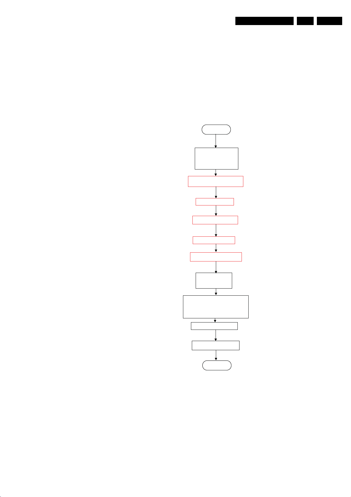
5.7.2 Start-up/Shut-down Flowcharts
EN 17LC8.1E LB 5.
On the next pages you will find start-up and shut-down
flowcharts, followed by a trouble shooting flowchart, which
might be helpful during fault finding.
Please note that some events are only related to PDP sets, and
therefore not applicable to this LCD chassis.
Page 18
EN 18 LC8.1E LB5.
Service Modes, Error Codes, and Fault Finding
AC ON
3V3STBY Available
Weltrend Powered by
3V3_STBY, STANDBY=HIGH
Power_ON_OFF=Low initialize
GPIO pins of Weltrend
Enable Audio mute
STANDBY=Low
Wait for 100ms
Wait for 100ms
Time out = 200ms
Weltrend to go
to Standby
NO
Weltrend reset the LOCTOP
CPU_RST=HIGH
NO
Enable Power Down
Enable DC_PROT INT
Initialize tuner, SMICL,
HDMI_MUX_RST
LCD_POWER_ON=HIGH
Is Power Down
=high?
YES
Wait for 300ms
LOCTOP read the NVM
Last status on?
YES
Wait for 20 ms
Switch ON LVDS Signal
Wait for 1000ms
Init. Warm Component
BL_ON_OFF=HIGH
*BL_ADJ KEEP 100% for
3000ms before dimming
Blank picture
Picture Mode setup & Detection
UnBlank Picture &
Unmute Audio
END
Figure 5-6 Start-up flowchart
I_18170_034.eps
310708
Page 19
Service Modes, Error Codes, and Fault Finding
Start
Mute Audio
ANTI_PLOP=LOW
MUTEn=HIGH
BL_ON_OFF=LOW
EN 19LC8.1E LB 5.
Note:
Total wait time 232ms iso 320ms
Audio is mute continuously -->
Wait 300ms
Switch OFF LVDS
Wait 20ms
LCD_PWR_ON=LOW
WP for NVM
LOCTOP
Enable Audio mute
Port assignment in STANDBY
( Weltrend)
STANDBY=HIGH
Disable Audio Mute?
END
I_18170_035.eps
310708
Figure 5-7 Stand-by flowchart
Page 20
EN 20 LC8.1E LB5.
Service Modes, Error Codes, and Fault Finding
Start
END
NO
POWER_DOWN=LOW
for 5 times ?
YES
Mute Audio & Video
WP for NVM
LOCTOP
STANDBY=HIGH
Wait 5000ms
Re-start:Start up
END
Figure 5-8 Power Down flowchart
I_18170_037.eps
310708
Page 21
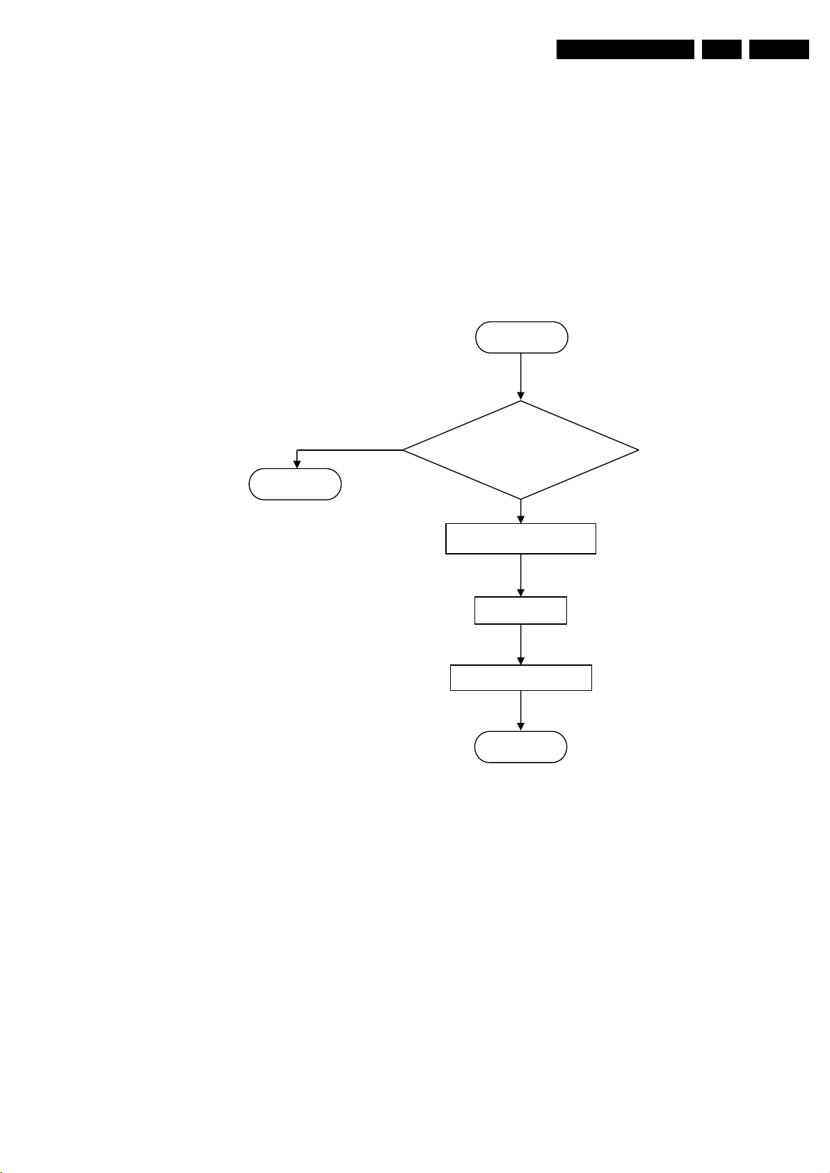
Service Modes, Error Codes, and Fault Finding
Start
EN 21LC8.1E LB 5.
END
NO
DC_PROT=Low
for 3seconds?
YES
Mute Audio & Video
WP for NVM
STANDBY=HIGH
END
I_18170_036.eps
310708
Figure 5-9 DC_PROT flowchart
Page 22

EN 22 LC8.1E LB5.
Personal Notes:
Service Modes, Error Codes, and Fault Finding
E_06532_012.eps
131004
Page 23

Block Diagrams, Test Point Overview, and Waveforms
6. Block Diagrams, Test Point Overview, and Waveforms
Wiring Diagram 32" (MG8)
23LC8.1E LB 6.
WIRING 32"
INVERTER
KEYBOARD CONTROL
(1007)
E
J1
1. GND
2. KEYBOARD
3. +3V3STBY
4. INTERRUPT
(STYLING MG8)
8P11
14P
LCD DISPLAY
LVD S INPUT
30P
x418
14. PDIM_Select
13. PWM
12. BL_ON_OFF
11. BOOST
10. GND3
9. GND3
8. GND3
7. GND3
6. GND3
5. 24Vinv
8418
4. 24Vinv
3. 24Vinv
2. 24Vinv
1. 24Vinv
X001
2. L
1. N
MAIN POWER SUPPLY
(1005)
8001
INLET
X416
1. 3.3V stby
2. STANDBY
3. GND1
4. GND1
5. GND1
6. +12V
7. +12V
8. +12V
9. +12V (audio)
10. GND2 (audio)
11. -12V (audio)
X419
1. +12V
2. +12V
3. GND1
4. GND1
5. BL_ON_OFF
6. DIM
7. BOOST
8. ANALOG_PWM
(1004)
8R50
8P01
8P02
SSB
(1150)
B
1303
(B03)
9. POWER_ONOFF
8. +5V_SW
7. KEYB
6. LED1
5. +3V3_STBY
4. LED2
3. REMOTE_IN
2. GND
1. N.C.
1R50
(B04C)
1. VDISP
3. VDISP
5. VDISP
7. VDISP
.
.
30. GND
1P02
(B01)
8. GND
7. BL_BOOST
6. BL_ADJUST_PWM
5. BL_ON_OFF_2
4. GND
3. GND
2. +12V_DISP
1. +12V_DISP
1P01
(B01)
11. -12V_AUDIO
10. GNDSND
9. +12V_AUDIO
8. +12V_DISP
7. +12V_DISP
6. +12V_DISP
5. GND
4. GND
3. GND
2. STANDBY
1. +3V3_STBY
1A35
(B05B)
4. ROUT_SP
3. ROU T_SP_GROUND
2. LOUT_SP_GROUND
1. LOUT_SP
1P11
1. GND
2. KEYBOARD
IR LED PANEL
J
(1112)
4. TACT_SWITCH_INT
3. +3V3STBY
1P10
1. LIGHT-SENSOR
2. GND
8A35
8303
+ -
6. LED1
7. KEYBOARD
8. +5V_SW
4. LED2
5. +3V3-STBY
9. TACT_SWITCH_INT
RIGHT SPEAKER
(5211)
3. IR
+ -
LEFT SPEAKER
(5212)
I_18170_015.eps
300708
Page 24

Block Diagrams, Test Point Overview, and Waveforms
Wiring Diagram 42" (MG8)
24LC8.1E LB 6.
WIRING 42"
KEYBOARD CONTROL
(1007)
E
J1
1. GND
2. KEYBOARD
3. +3V3STBY
4. INTERRUPT
(STYLING MG8)
2P3
DANGEROUS
HIGH VOLTAGE
8P11
TO BACK LIGHT
DANGE ROUS
HIGH VOLTAGE
x403
1. HV1
2. N.C.
MAIN POWER SUPPLY
(1005)
DANGEROUS
HIGH VOLTAGE
3. HV 1
x402
1. HV2
2. N.C.
3. HV 2
X416
1. 3.3V stby
2. STANDBY
3. GND1
4. GND1
5. GND1
6. +12V
7. +12V
8. +12V
9. +12V (audio)
10. GND2 (audio)
11. -12V (audio)
X419
1. +12V
2. +12V
3. GND1
4. GND1
5. BL_ON_OFF
6. DIM
7. BOOST
8. ANALOG_PWM
X001
2. L
1. N
LCD DISPLAY
LVD S INPUT
30P
8P01
8P02
(1004)
8R50
SSB
(1150)
B
1303
(B03)
9. POWER_ONOFF
8. +5V_SW
7. KEYB
6. LED1
5. +3V3_STBY
4. LED2
3. REMOTE_IN
2. GND
1. N.C.
1R50
(B04C)
1. VDISP
3. VDISP
5. VDISP
7. VDISP
.
.
30. GND
1P02
(B01)
8. GND
7. BL_BOOST
6. BL_ADJUST_PWM
5. BL_ON_OFF_2
4. GND
3. GND
2. +12V_DISP
1. +12V_DISP
1P01
(B01)
11. -12V_AUDIO
10. GNDSND
9. +12V_AUDIO
8. +12V_DISP
7. +12V_DISP
6. +12V_DISP
5. GND
4. GND
3. GND
2. STANDBY
1. +3V3_STBY
1A35
(B05B)
4. ROUT_SP
3. ROU T_SP_GROUND
2. LOUT_SP_GROUND
1. LOUT_SP
2P3
DANGEROUS
HIGH VOLTAGE
TO BACK LIGHT
1P11
1. GND
2. KEYBOARD
IR LED PANEL
J
(1112)
3. +3V3STBY
4. TACT_SWITCH_INT
1P10
1. LIGHT-SENSOR
2. GND
3. IR
4. LED2
5. +3V3-STBY
6. LED1
7. KEYBOARD
8. +5V_SW
9. TACT_SWITCH_INT
8303
+ -
RIGHT SPEAKER
(5211)
8001
INLET
8A35
+ -
LEFT SPEAKER
(5212)
I_18170_016.eps
300708
Page 25

Block Diagrams, Test Point Overview, and Waveforms
Block Diagram Video
VIDEO
TUNER IF & SAWF
B02
1104
UV1316E
MAIN
TUNER
VST
9
AGC
VTUN
IF_ATV
11
IF1
1
IO - SCART 1
B06B
EXT 1
IO - SCART 2
B06C
EXT 2
B06A
YPBPR & SVHS
SVHS IN
EXT 3
RF_AGC
16
20
SCART1
16
20
SCART2
CVBS
PR
PB
Y
25LC8.1E LB 6.
SMIC L
B05A
7401
TDA8890H1
1102
15
2
3
SAW 38M9
1103
1
2
3
SAW 38M9
7109
1504
15
1
7
11
7
11
20
15
21
1E01
1
7
11
15
21
1602
1601
1
5
2
1614
7503
19
16
8
7E01
19
15
8
20
3
4
SC2_Y_CVBS_IN
SVHS_Y_CVBS_IN
VIF1
4
VIF2
4
SIF1
SIF2
5
SAW_SW
SC1_R_IN
SC1_B_IN
SC1_G_IN
SC1_CVBS_IN
SC1_RF_OUT_CVBS
SC1_FBL_IN
SC1_STATUS
SC2_CVBS_MON_OUT
SC2_C_IN
SC2_STATUS
SVHS_C_IN
HD_PR_IN
HD_PB_IN
HD_Y_IN
72
71
68
67
SMIC
79
66
30
28
29
50
53
31
39
44
42
25
24
23
11
12
46
16
17
B04A
TDA154XX
MON_CVBS
PIP_R
PIP_G
PIP_B
TDA889X_HS
TDA889X_VS
MAIN_CVBS_Y
MAIN_C
SC1_FBL_IN
SC1_STATUS
SC2_C_IN
SC2_STATUS
SC2_Y_CVBS_IN
HD_PR_IN
HD_PB_IN
HD_Y_IN
7C01
TDA15471HV
18
15
17
252
253
30
25
24
16
23
26
4
27
11
10
8
ANALOGUE
LOC TOP
LVD S
MEMORY
MISC
189
188
187
186
185
184
183
182
181
180
199
198
201
LVDS CONNECTORS
B04C
DDR FLASH TRAP
B04B
MD(0-15)
MA(0-11)
SPI_SDO
SPI_SDI
SPI_SCK
TXCLKn
TXCLKp
7701
HY5DU281622FTP
DDR
SDRAM
2Mx16x4
7702
M25P80
2
8M
5
FLASH
6
TXAn
TXAp
TXBn
TXBp
TXCn
TXCp
TXDn
TXDp
1R10
1R11
1R12
1R13
1R14
VDISP
TXAn1
TXAp1
TXBn1
TXBp1
TXCn1
TXCp1
TXCLKn1
TXCLKp1
TXDn1
TXDp1
1R50
12
14
18
20
24
26
30
1
3
5
7
2
4
6
8
CONNECTOR
LVDS
B06D
CONNECTOR
HDMI
HDMI
1N01
RX2_A+
1
RX2_A-
1
19
3
RX1_A+
4
RX1_A-
6
RX0_A+
7
RX0_A-
9
18 2
10
RXC_A+
12
RXC_A-
HDMI_MUX_TX2+
HDMI_MUX_TX2-
HDMI_MUX_TX1+
HDMI_MUX_TX1-
HDMI_MUX_TX0+
HDMI_MUX_TX0-
HDMI_MUX_TXC+
HDMI_MUX_TXC-
7N07
IP4776CZ38
27
30
INTERFACE
33
HDMI
HDMI_MUX_TX2+
HDMI_MUX_TX2-
HDMI_MUX_TX1+
HDMI_MUX_TX1-
HDMI_MUX_TX0+
HDMI_MUX_TX0-
HDMI_MUX_TXC+
HDMI_MUX_TXC-
10
7
4
245
244
241
240
237
236
233
232
HDMI
I_18170_017.eps
300708
Page 26

Block Diagrams, Test Point Overview, and Waveforms
Block Diagram Audio
AUDIO
TUNER IF & SAWF
B02
1104
UV1316E
MAIN
TUNER
IF1
AGC
VST
9
VTUN
IO - SCART 1
B06B
1
7
EXT 1
11
15
16
20
21
SCART1
26LC8.1E LB 6.
SMIC L
B05A
7401
TDA8890H1
1102
15
2
4
3
SAW 38M9
1103
IF_ATV
11
1504
RF_AGC
6
2
3
1
SC1_AUDIO_IN_L
SC1_AUDIO_IN_R
SC1_AUDIO_OUT_L
SC1_AUDIO_OUT_R
1
1
2
3
SAW 38M9
7109
4
5
VIF1
VIF2
SIF1
SIF2
SAW_SW
72
71
68
67
SMIC
79
66
52
51
62
61
7
9
10
4
5
B04A
TDA154XX
TUN_SIF
MAIN_L
MAIN_R
TUN_L
TUN_R
7C01
TDA15471HV
53
LOC TOP
37
38
55
56
61
62
71
B05B
AUDIO_LS__L
AUDIO_LS__R
POWER_DOWN
B03
B03
AUDIO CLASS D
7A01
TDA8932T/N1
37
38
MUTEn
CLASS D
POWER
AMPLIFIER
MUTING
CIRCUIT
DC_PROT
ENGAGE
27
22
5
7J42
DC-DETECTION
LOUT_SP
ROUT_SP
1A35
1
2
3
4
Speaker L
Speaker R
B05B
B06C
B06A
B06D
AUDIO CLASS D
IO - SCART 2
EXT 1
16
20
SCART1
YPBPR & SVHS
AUDIO IN
L+R
AUDIO IN
L+R
HDMI
1
18 2
19
HDMI
CONNECTOR
B06A
SC1_AUDIO_MUTE_L
SC1_AUDIO_MUTE_R
SC2_AUDIO_MUTE_L
SC2_AUDIO_MUTE_R
1504
1
3
7
1
11
6
15
2
21
1602
1615
1N01
1
3
4
6
7
9
10
12
SC2_AUDIO_OUT_L
SC2_AUDIO_OUT_R
SC2_AUDIO_IN_L
SC2_AUDIO_IN_R
SIDE_AUDIO_IN_L
SIDE_AUDIO_IN_R
COMP_AUDIO_IN_L
COMP_AUDIO_IN_R
RX2_A+
RX2_A-
RX1_A+
RX1_A-
RX0_A+
RX0_A-
RXC_A+
RXC_A-
CONTROL
ANTI
PLOP
HDMI_MUX_TX2+
HDMI_MUX_TX2-
HDMI_MUX_TX1+
HDMI_MUX_TX1-
HDMI_MUX_TX0+
HDMI_MUX_TX0-
HDMI_MUX_TXC+
HDMI_MUX_TXC-
ANTI_PLOP
B03
7N07
IP4776CZ38
27
30
INTERFACE
33
41
40
48
45
64
63
35
34
HDMI
68
HDMI_MUX_TX2+
HDMI_MUX_TX2-
HDMI_MUX_TX1+
HDMI_MUX_TX1-
HDMI_MUX_TX0+
HDMI_MUX_TX0-
HDMI_MUX_TXC+
HDMI_MUX_TXC-
10
7
4
245
244
241
240
237
236
233
232
HDMI
YPBPR & SVHS
HP_DETECT
LOUT_HP
ROUT_HP
1603
2
3
6
Headphone
Out 3.5mm
I_18170_018.eps
300708
Page 27

Block Diagrams, Test Point Overview, and Waveforms
Block Diagram Control & Clock Signals
CONTROL & CLOCK SIGNALS
E
KEYBOARD CONTROL
CHANNEL +
CHANNEL -
MENU
VOLUME -
VOLUME +
ON / OFF
J
IR LED PANEL
TAC T _ SWITCH_INT
6P11
+5V_SW
+3V3STBY
+3V3STBY
3P11
3P10
3P16
LED1
WHITE
6P10
LED2
RED
7P14
7P11
7P10
IR
SENSOR
J1
2
4
1P11
2
4
1P10
9
+5V_SW +5V_SW
KEYBOARD
LED1
+3V3STBY +3V3STBY
LED2
IR
88
7
66
55
44
33
22
11
B03
MICROPROCESSOR NVM
1303
9
7
POWER_ONOFF
4313
N.C.N.C.
KEYB
LED1
LED2
REMOTE
7303
WT61P8S
44
MICRO
PROCESSOR
19
24
25
9
27LC8.1E LB 6.
B04A
POWER_ONOFF_LOCTOP
KEYB
REMOTE
10
B06D
HDMI
1N01
13
HDMI
CONN.
38
37
6
26
37
4
3
ANTI_PLOP
MUTEn
CPU_RST
DDC_RST_A
1312
12M
+3V3STBY
4314
7304
7N03
B05B
(AUDIO)
B05B
B06D
TDA154XX
B06A
B05B
HDMI_CECHDMI_CEC_A
HP_DETECT
DC_PROT
WT_LOCTOP
BL_BOOST_PWM
BL_ON_OFF
BL_ADJ
7C01
TDA15471HV
75
33
197
195
68
71
194
219
220
215
196
LOC TOP
225
1C01
27M
226
182
183
63
64
214
216
B04B
MD(0-7)
MA(0-19)
SDCLKP
163
162
SDCLKN
SPI_SDI
198
201
SPI_SCK
SPI_SDO
199
200
SPI_CEN
B01
BL_ADJUST_PWM
TxCLKp
TxCLKn
SMIC_CLKP
SMIC_CLKP
HPD_RST_MUX
LCD_PWR_ON
B04C
B04C
B05B
B05B
B06D
B04C
DDR FLASH TRAP
7701
HY5DU281622FTP
DDR
SDRAM
2Mx16x4
45
46
7702
M25P80
5
6
8M
2
FLASH
1
DC/DC +5V & +3V3 & +2V5
& +1V8 & +8V
1P02
6
+3V3_STBY
5
7309
BD45275G
VOUT
2,3
MP_RST
4
43
41
7301
7305
BL_ON_OFF_2
BL_BOOST
STANDBY
5
7
1P02
6
I_18170_019.eps
210708
Page 28

Block Diagrams, Test Point Overview, and Waveforms
SSB: Test Points (Overview Bottom Side)
28LC8.1E LB 6.
3139 123 6425.1
Part 1
I_18170_014a.eps
Part 2
I_18170_014b.eps
I_18170_014.eps
310708
A115 C1
A116 C1
A124 C1
A125 C1
F101 C1
F102 B1
F103 B1
F104 B1
F105 B1
F106 A1
F107 A1
F108 A1
F109 A1
F110 A1
F111 A1
F112 A1
F113 B2
F114 C1
F115 B1
F116 C1
F117 C1
F118 B1
F301 B2
F302 A3
F303 A2
F304 A2
F305 A2
F306 B2
F307 B2
F308 B4
F309 B4
F310 B4
F311 B4
F313 B4
F314 B4
F315 C1
F316 C1
F317 A3
F318 C1
F319 A2
F320 A2
F321 B4
F322 A2
F323 A3
F324 B3
F325 A3
F
327 C3
F328 A2
F330 C3
F331 C3
F333 B3
F334 B3
F335 B4
F336 B1
F337 B2
F338 A2
F339 A2
F340 A2
F341 A2
F342 A2
F343 A2
F344 A2
F345 A2
F401 C1
F402 C1
F403 C1
F404 C1
F405 C1
F406 C1
F407 C1
F511 F1
F513 E1
F515 E1
F517 E1
F519 E1
F520 E1
F521 E1
F522 E1
F524 E1
F525 E1
F526 D1
F528 D1
F530 D1
F531 E1
F534 E1
F535 E1
F536 E1
F537 E1
F538 E1
F539 E1
F540 E1
F541 E1
F542 E1
F601 A1
F602 A1
F603 A1
F604 E1
F605 D1
F606 C1
F607 E1
F608 E1
F609 F1
F610 B1
F611 B1
F612 B1
F613 C1
F614 E1
F615 A1
F616 F1
F617 F1
F618 F1
F619 F2
F620 F1
F701 C3
F702 C3
F703 C3
F704 C3
F705 C3
F706 C3
F707 C3
F708 C3
F709 C3
F710 C4
F711 C3
F712 C3
FA01 F3
FA02 E3
FA0 3 F2
FA04 F2
FA05 F2
FA06 F3
FA07 F4
FA0 8 F4
FA09 F2
FA10 F4
FA11 F4
FA12 F2
FA1 3 F2
FA14 E3
FA15 A3
FA32 F2
FA33 F3
FC01 C2
FC02 B2
FC03 B3
FC04 D2
FC05 D2
FC06 D2
FC07 D2
FC08 D1
FC09 C2
FC10 B3
FC11 B2
FE01 F1
FE02 E1
FE03 E1
FE04 E2
FE05 E1
FE06 E1
FE07 E1
FE08 D2
FE09 D1
FE10 D1
FE12 C3
FE15 B2
FE16 B2
FE17 B3
FE18 C3
FE19 C3
FE20 C3
FE21 C4
FE22 F1
FE23 E1
FE24 E1
FE25 E1
FE26 E1
FE27 E1
FE28 D1
FE29 D1
FE30 E1
FE31 E1
FN01 E3
FN02 D2
FN03 E3
FN04 D2
FN05 D3
FN06 D3
FN07 D3
FN08 D3
FN09 D3
FN10 D2
FN11 D2
FN12 D2
FN13 D2
FN14 D2
FN15 E3
FN16 E3
FN17 D3
FN18 D3
FN19 E3
FN20 E3
FN21 E3
FN22 E3
FN23 E2
FN24 E2
FN74 D3
FP01 E4
FP02 E4
FP03 D4
FP04 D4
FP05 D4
FP06 F4
FP07 F4
FP08 D4
FP09 E4
FP10 D4
FP11 D4
FP12 D4
FP13 D4
FP14 F4
FP15 E4
FP16 A3
FP17 E3
FP18 B3
FP19 A4
FP20 A3
FP21 F4
FP22 A3
FP23 F4
FR01 C4
FR02 C4
FR03 C4
FR04 C4
FR05 C4
FR06 C4
FR07 C4
FR08 C4
FR09 C4
FR10 C4
FR11 C4
FR12 C4
FR13 C3
I102 B1
I103 C1
I105 B1
I106 B1
I108 B2
I109 C1
I301 A2
I302 C3
I304 A2
I305 A3
I306 A3
I307 A2
I308 B4
I310 A2
I311 A3
I314 B1
I315 A2
I316 A2
I317 A2
I318 C2
I319 A2
I320 C3
I321 A2
I323 A2
I324 A3
I325 A3
I326 A3
I327 A2
I328 A2
I331 A2
I332 A2
I333 A2
I334 D3
I401 D1
I402 D1
I403 D1
I404 D1
I405 D1
I406 C1
I407 D1
I408 D1
I410 C1
I411 C1
I416 D1
I417 D1
I418 D1
I419 D1
I420 D1
I421 C1
I422 C1
I423 D1
I427 C1
I430 C1
I431 C1
I432 C1
I433 C1
I434 C1
I435 C1
I436 C1
I437 C1
I438 C1
I439 C1
I440 C1
I441 C1
I442 C1
I443 C1
I444 C1
I445 C1
I446 C1
I447 C1
I448 C1
I449 D1
I450 D1
I451 C1
I452 D1
I453 D1
I454 C1
I455 C1
I525 E1
I541 E1
I548 E1
I549 D1
I550 E1
I553 E1
I610 E1
I611 F1
I621 B1
I623 E1
I624 C1
I627 F1
I701 C3
IA01 F2
IA02 F2
IA03 F2
IA04 F3
IA05 F2
IA06 F2
IA07 F2
IA08 F3
IA09 F2
IA10 E2
IA11 E2
IA12 E2
IA13 F2
IA14 F2
IA15 F2
IA16 F2
IA17 E2
IA18 F2
IA19 F2
IA21 F2
IA22 F2
IA30 F3
IA31 F3
IA33 F2
IA35 F3
IA36 F3
IA38 F3
IA39 F3
IA42 B2
IA44 C1
IA45 C1
IA48 C1
IA49 C1
IA50 F1
IA51 F1
IA52 F1
IA53 F1
IA67 A3
IA68 B3
IA69 A3
IA70 A
IA71 A3
IA72 A3
IA73 F3
IC01 C2
IC02 C2
IC03 C2
IC04 C2
IC05 C2
IC06 D2
IC07 C2
IC08 C2
IC09 C2
IE01 D1
IE02 D1
IE03 D1
IE04 D1
IN01 D3
IN02 D3
IN03 D2
IN04 D2
IN06 D3
IN07 D2
IN10 D2
IN11 D2
IN12 D2
IN13 D3
IN14 D3
IN15 E3
IN16 E3
IN17 D3
IN18 D3
IN19 D2
IN20 D2
IP01 E4
IP02 E4
IP03 E4
IP04 E4
IP05 E4
IP06 E4
IP07 E4
IP08 E4
IP09 E4
IP10 A3
IP11 A4
IP12 F4
IP13 E3
IP14 F4
IP15 F4
IP16 E4
IP17 E4
IP18 F4
IP19 E4
IP20 E4
IP21 E3
IP22 E4
IP23 A3
IP24 A4
IP25 E4
IP26 E4
IP27 E4
IP28 E4
IP29 E4
IP30 E3
IP31 E4
IP32 E4
IP33 E4
IP34 E3
IP35 E4
IP37 E4
IP38 E4
IP39 E4
IP40 E4
IP41 E4
IP42 E4
IP43 F4
IR01 C4
IR02 C3
IR03 C3
IR04 C4
IR05 C3
3
Page 29

Block Diagrams, Test Point Overview, and Waveforms
SSB: Test Points (Part 1 Bottom Side)
29LC8.1E LB 6.
Part 1
I_18170_014a.eps
210708
Page 30

Block Diagrams, Test Point Overview, and Waveforms
SSB: Test Points (Part 2 Bottom Side)
30LC8.1E LB 6.
Part 2
I_18170_014b.eps
310708
Page 31

I2C IC Overview
I²C
B03
MICROPROCESSOR NVM
Block Diagrams, Test Point Overview, and Waveforms
B04A
TDA154XX
31LC8.1E LB 6.
TUNER IF & SAWF
B02
B05A
SMIC L
B06C
SCART2 & UART & JTAG
7303
WT61P8S
MICRO
PROCESSOR
DS1-DA
DS1-CL
20
21
ERR
04
UART
SERVICE
CONNECTOR
+3V3_STBY
3309
3304
1311
IIC_SDA
IIC_SCL
3322
EEPROM
3
2
3323
56
7302
M24C32
NVM
ERR
06
3348
3349
MAIN_NVM_WC
7
UART_RXD
UART_TXD
+3V3_SW
3C35
3C03
3C40
76
192
193
5C19
TDA15471HV
LOC TOP
5C20
66 67
7C01
3101
UV1316E/ABH
B06D
IIC_SDA
IIC_SCL
3102
54
1104
TUNER
ERR
07
HDMI
3410
TDA8890H1
+3V3_SW
3411
14 13
7401
SMIC
ERR
08
3E70
3E71
1E04
1
2
3
COMPAIR
SERVICE
CONNECTOR
B04B
DDR FLASH TRAP
7702
M25P80
8M
FLASH
7701
HY5DU281622FTP
DDR
SDRAM
2Mx16x4
2
5
6
SPI_SDO
SPI_SDI
SPI_SCK
MD(0-15)
MA(0-11)
199
198
201
217
218
3C64
3C65
HDMI_MUX_TSDA
HDMI_MUX_TSCL
18 17
7N07
IP4776CZ38
HDMI
INTERFACE
21
22
3N06
3N05
+5V_SW
3N09
3N10
56
7N01
M24C02
EEPROM
DDC_SDAA
DDC_SCLA
7N08
1N01
16
HDMI A
15
DDC_RST_A
1
18 2
19
HDMI
CONNECTOR
B03
I_18170_020.eps
300708
Page 32

Block Diagrams, Test Point Overview, and Waveforms
Supply Lines Overview
SUPPLY LINES OVERVIEW
A
X419
+12V
+12V
GND1
GND1
MAIN
POWER SUPPLY
BL-ON_OFF
DIM
BOOST
ANALOG_PWM
X416
3.3Vstby
STANDBY
GND1
GND1
GND1
+12V
+12V
+12V
12V (audio)
GND2( audio)
-12VA (audio)
1 1
2
3
4
5
6
7
8
1 1
2
3
4
5
6
7
8
9
10
11
B01
1P02
2
3
4
5
6
7
8
1P01
2
3
4
5
6
7
8
9
GNDSND
10
11
7P08
NCP5422
Dual
Out-of-Phase
Synchronous
Buck Controller
DC / DC +5V & +3V3 & +2V5 +1V8 & +1V2
5P02
3P20
5P10
5P07
7P06-1
14
1
7P06-2
2
7P07-1
16
7P07-2
15
BL_ON_OFF_2
BL_ADJUST_PWM
BL_BOOST
STANDBY
7P10
6P03
5P06
7P09
ONLY FOR ANALOG TUNER
5P09
5P08
5P04
5P03
(CONTROL)
(CONTROL)
(CONTROL)
+5V_SW
5P01
7P04
IN OUT
COM
7P01
IN OUT
COM
7P02
IN OUT
COM
7P03
IN OUT
COM
5P05
B03
B03
B03
+3V3_STBY
B04A
+12V_DISP
+8V_SW
+12V_AUDIO
-12V_AUDIO
+VTUN
(34V)
+5V_SW
+3V3_SW
+2V5_SW
+3V3_SW_TDA
+1V8_SW_ADC
+1V8_SW
B03,B04a,B05b,
B06d
B03,B04c
B05a
B05b
B05b
B02
B02,B03,B05a,
B06b,c,d
B03,B04a,b,
B05a,B06a,d
B04a,b
B04a
B04a
B04A,B06d
32LC8.1E LB 6.
AUDIO - CLASS D
+12V_AUDIO
3A01
-12V_AUDIO
3A02
+3V3_STBY
YPBPR & SVHS
+3V3_SW
I/0 - SCART 1
SCART 2 & UART & JTAG
HDMI
+3V3_SW
5N01
+1V8_SW
5N02
5N03
HDMI
CONNECTOR
HDMI
CONNECTOR
J
5
8
1N01
18
1N02
18
RES
IR & LED PANEL
5A05
5A06
+12V_AUDIO
VDDA
VDD
-12V_AUDIO
VSSA
VSS
+3V3_STBY
+3V3_SW
+5V_SW+5V_SW
+5V_SW+5V_SW
+3V3_SW
+3V3_ANA-MUX
+3V3_STBY+3V3_STBY
+1V8_SW
+1V8_DIG-MUX
+1V8_ANA-MUX
+5V_SW+5V_SW
+5VHDMI_A
+5VHDMI_B
+3V3STBY
+5V_SW
I_18170_021.eps
310708
B01
B01
B01
B01
B01
B01
B01
B01
B01
B01
B01
B01
B01
B01
B01
B01
B01
B01
TUNER IF & SAWF
B02
+5V_SW
+VTUN
MICROPROCESSOR NVM
B03
+3V3_SW
+3V3_STBY
+5V_SW
+12V_DISP
B04A
B04B
B04C
B05A
TDA154XX
+3V3_SW
+3V3_SW_TDA
+3V3_STBY
+2V5_SW
+1V8_SW_ADC
+1V8_SW
DDR FLASH TRAP
+2V5_SW
+3V3_SW
LV DS CONNECTORS
+12V_DISP
SMIC L
+5V_SW
+3V3_SW
+8V_SW
3107
5C11
5402
7R02
5115
3321
5R02
5R03
LCD_PWR_ON
+5V_SW
+5V_IF
+5V_TUN
+VTUN
+3V3_SW
+3V3_STBY
+5V_SW
+12V_DISP
5304
+3V3_SW
+3V3_SW_TDA
+3V3_STBY
+2V5_SW
+1V8_SW_ADC
+1V8_SW
+1V8_SW_LOCAL
+2V5_SW
+3V3_SW
+12V_DISP
+5V_SW_SMIC
+3V3_SW
VDISP
+5V_SW
+8V_SW
1303
1R50
B05B
B01
B01
B01
B06A
B01
8
5
B01
TO 1P10
J
I/R LED
B06B
B06C
B01
B06D
B01
B01
B01
B01
1
TO 1303
B03
SSB
1P10
Page 33

Circuit Diagrams and PWB Layouts
7. Circuit Diagrams and PWB Layouts
SSB: DC/DC
1
23 67891011
DC/DC +5V & +3V3 & +2V5 & +1V8 & +8V
B01
A
2P51
1u0
6P04
BAS316
IP05
7P06-1
2
7P06-2
SI4936BDY
3P26
2R2
3P30
3K3
3P05
+12V_DISP
IP03
IP06
1
4
3K3
PDZ8.2-B
3P24
3P27
78
SI4936BDY
2P32
3n3
IP17
IP18
3P36
470R
IP43
6P01
B
C
D
E
F
G
H
3139 123 6425.1
7P05
BC817-25W
+5V_SW
IP08
3P17
470R
1%
3P18
120R
1%
IP09
IP28
2P40
100n
GNDDC1
NCP5422ADR2G
FP02
IP29
IP30
2P41
100n
GNDDC1
3P19
1K8
GNDDC1GNDDC1
GNDDC1
GNDDC1
7P08
4
7
10
8
9
3P29
39K
GNDDC1
PDZ18-B
3P20
10R
2P31
1u0
BST
1
2
1
2
ROSC
2P49
220p
IP20
2P50
220p
IP35
GNDDC1
6P06
14
VFB
COMP
IP01
Φ
VCC
3
GNDDC1
GATE
GATE
GND
IP37
3P28
1K0
IP38
3P23
10R
IP04
1
H1
IP25
2
L1
H2
L2
+1
-1
IS
+2
-2
IP32
IP26
IP27
16
IP16
15
5
6
IP31
1213
11
IP39
"P00-P99"
MULTI 12NC: 3139 123 64241
SINGLE 12NC: 3139 123 64251
123456789
45
2P39
100n
2P42
100n
2P07
100n
5
3
3P32
2R2
3P34
2K2
3P03
1K8
6
3P08
3K3
68R
68R
3P13
10R
IP40
IP41
IP13
2P16
10u
16V
3P02
1K2
3P04
1K8
IP19
BAS316
7P07-2
SI4936BDY
3P01
6K8
3P07
6K8
3P35
220R
3P09
1K0
6P05
2P30
22u
7P07-1
IP42
2P37
4
78
SI4936BDY
2
1
3n3
56
3
+5V_SW
FP17
+1V8_SW
IP12
7P10
BC847B
FP21
+8V_SW
3P10
10K
+5V_SW
FP08
33LC8.1E LB 7.
IP14
GNDDC1
5P09
50R
2P48
100p
3P16
1K0
1
3P15
1K0
3P33
6K8
IP22
2P36
100n
3P31
1K0
3P22
6K8
IP21
2P54
100n
IP34
3P21
1K0
3P11
6K8
GNDDC1
IP11
2P01
100u
16V
3
7P09
2N7002
2
GNDTUN
5P01
22u
5P05
22u
3
2P02
100n
5P06
1m0
IP15
2P20
6P03
100p
FP23
ONLY FOR ANALOG TUNER
2P33
3n3
IP07
3n3
2P43
GNDDC1
7P04
LD1117S33
COM
3P12
390R
1%
3P14
470R
1%
OUTIN
1
GNDDC1
FP22
2
4
2P03
47u
16V
2P58
22u
IP02
BAV99
2P34
22u
+3V3_SW
RES
2P56
22u
5P02
10u
2P19
22u
35V
RES
2P55
22u
FP03
+3V3_SW_TDA
FP14
FP05
IP33
+1V8_SW
+5V_SW
+5V_SW
6P02
PDZ33-B
+12V_DISP
+VTUN
34V
+5V_SW
5P08
50R
5P03
50R
5P04
50R
STANDBY
+12V_DISP
+12V_AUDIO
-12V_AUDIO
GNDSND GNDSND
BL_ON_OFF_2
BL_ADJUST_PWM
BL_BOOST
IP23
2P17
220u
25V
IP24
2P04
100u
16V
IP10
2P13
100u
16V
5P10
5P07
10n2P08
100n
2P25
GNDSND
/BL_ADJUST_ANA
3
2P18
100n
3
2P05
100n
3
2P14
100n
+3V3_STBY
22u
22u
1n0
100n
2P09
2P26
GNDSND
7P01
LD1117S25C
OUTIN
COM
1
7P02
LD1117S33
OUTIN
COM
1
7P03
LD1117S18
OUTIN
COM
1
2P10 10n
2P23 100n
2P24
1n0
2P11
GNDSND
FP11
FP12
FP13
2
FP18
4
2
4
FP20
2
4
2P21
47u
16V
2P15
47u
16V
100n
2P12 100n
FP19
FP01
FP16
FP15
FP04
FP06
FP07
FP09
1-1735446-1
1P02
FP10
1735446-8
2P06
47u
16V
+1V8_SW_ADC
1P01
1
2
3
4
5
6
7
8
+3V3_SW_TDA
10 11 12
1
2
3
4
5
6
7
8
9
10
11
2P27
2P44
2P45 1n0
2P47
+2V5_SW
12
B01
100n
1n0
1n0
I_18170_001.eps
170708
A
B
C
D
E
F
G
H
1P01 A12
1P02 B11
2P01 F7
2P02 F7
2P03 F8
2P04 E10
2P05 E10
2P06 F11
2P07 B4
2P08 B10
2P09 B10
2P10 B11
2P11 B11
2P12 B11
2P13 F10
2P14 F10
2P15 F11
2P16 G4
2P17 E10
2P18 D10
2P19 A9
2P20 B8
2P21 D11
2P23 A11
2P24 A11
2P25 B10
2P26 B11
2P27 B12
2P30 B5
2P31 C2
2P32 C4
2P33 C7
2P34 C8
2P36 C7
2P37 D5
2P39 E4
2P40 E2
2P41 E2
2P42 E4
2P43 D7
2P44 B12
2P45 B12
2P47 B12
2P48 E7
2P49 F2
2P50 F2
2P51 A4
2P54 E7
2P55 C9
2P56 D9
2P58 D8
3P01 D5
3P02 E5
3P03 E4
3P04 E5
3P05 E4
3P07 E5
3P08 F4
3P09 F5
3P10 G5
3P11 E7
3P12 D8
3P13 D4
3P14 E8
3P15 B7
3P16 A7
3P17 D2
3P18 F2
3P19 F2
3P20 B2
3P21 E7
3P22 D7
3P23 C3
3P24 A4
3P26 D4
3P27 A4
3P28 B3
3P29 E2
3P30 E4
3P31 C7
3P32 D4
3P33 C7
3P34 D4
3P35 F5
3P36 G4
5P01 B7
5P02 A9
5P03 F10
5P04 E10
5P05 D7
5P06 A7
5P07 B10
5P08 D10
5P09 F7
5P10 A10
6P01 G4
6P02 A9
6P03 B8
6P04 A4
6P05 A5
6P06 B3
7P01 D11
7P02 E11
7P03 F11
7P04 F8
7P05 A3
7P06-1 B4
7P06-2 C4
7P07-1 C5
7P07-2 D5
7P08 D2
7P09 B7
7P10 F5
FP01 A11
FP02 D2
FP03 D9
FP04 A11
FP05 B9
FP06 A11
FP07 B11
FP08 B6
FP09 B11
FP10 B11
FP11 B11
FP12 B11
FP13 B11
FP14 A9
FP15 A11
FP16 A11
FP17 E5
FP18 D11
FP19 E11
FP20 F11
FP21 G6
FP22 F8
FP23 B8
IP01 C3
IP02 A8
IP03 C4
IP04 C3
IP05 B4
IP06 B4
IP07 C7
IP08 D2
IP09 D2
IP10 F10
IP11 F7
IP12 F5
IP13 E4
IP14 A7
IP15 A8
IP16 D4
IP17 D4
IP18 F4
IP19 A5
IP20 F2
IP21 D7
IP22 C7
IP23 D10
IP24 E10
IP25 D3
IP26 D4
IP27 D4
IP28 D2
IP29 D2
IP30 E2
IP31 D4
IP32 F3
IP33 A9
IP34 E7
IP35 G2
IP37 B3
IP38 B3
IP39 E3
IP40 D4
IP41 D4
IP42 C5
IP43 G4
Page 34

SSB: Tuner IF & SAWF
Circuit Diagrams and PWB Layouts
34LC8.1E LB 7.
1234
5678910
11 12
TUNER IF & SAWF
B02 B02
A
RES
I103
1
2
3
1
2
3
F117
2112
22u
1102
I
GND
OFWK3953M
38M9
1103
I
GND
OFWK9656M
38M9
3111
5K6
6101
BAS316
2106
2u2
5
O1
4
O2IGND
5
O1
4
O2ISWI
+5V_IF
3110
8K2
3105
39K
A115
A116
A125
A124
F118
VIF1
VIF2
SIF2
SIF1
RF_AGC
1104
1102
1103
4101
4102
4103
4104
EUROPE
UV1316E
K3953
K9656M
Y
-
Y
-
AP
UV1316E
K7257M
K9362
Y
-
Y
CHINA
UV1356
TBC
K9352
Y
-
-
Y
L ATAM
UV1336
M1971M
B
C
D
G
SAW FILTERS
F101
18K
NC1
6
F106
+5V_IF
VS
7
2113
10n
3112
2K2
7109
BC847B
VV1316
NC2
9
8
F107
F108
PLL
VST
10
F109
NC3
3109
2K2
IF111
+5V_IF
L
H
M
MT3
MT4
F110
3113
6K8
14
15
2114
100p
I102
4102
F114
+5V_TUN
2104
22u
4103
4104
F111
2105
10n
4101
F115
6103
1SS356
NC
+VTUN
3104
1K0
2103
2111
10u
100n
50V
IF_ATV
5111
RES
390n
SAW_SW
F116
3108
22K
I109
3103
PEND NEW 12NC FOR TD1316AF/BHPN-5
*
RF OUT
TU2
F103
L
H
M
AS3
TUNER
SDA
SCL
4
5
F105
F104
E
F
F112
NC
1104
UV1300
12
13
MT1
MT2
AGC
1
F102
1102 A7
1103 C7
1104 E1
2101 H3
2102 H3
2103 G5
2104 G5
2105 G6
2106 F7
A
2109 H11
2110 H11
2111 G4
2112 F7
2113 B3
2114 G3
3101 H4
3102 H4
3103 D2
3104 F4
3105 F7
3107 H10
B
3108 D2
3109 C3
3110 E7
3111 E7
3112 C2
3113 C3
4101 B5
4102 B5
4103 C6
4104 D6
4106 H6
C
4107 H6
5101 H4
5102 H4
5111 B2
5115 H11
6101 F7
6103 C3
7109 D2
A115 B8
A116 B8
A124 D8
A125 C8
D
F101 B2
F102 G1
F103 G2
F104 G2
F105 G2
F106 G2
F107 G2
F108 G3
F109 G3
F110 G3
F111 F6
F112 F1
E
F113 H11
F114 C5
F115 C3
-
Y
-
-
-
F116 D2
F117 D6
F118 E8
I102 C5
I103 D6
I105 H6
I106 H6
I108 H11
F
I109 D2
G
H
3139 123 6425.1
3101
100R
5101
2101
15p
2102
15p
RES
RES
1K0
3102
100R
1K0
5102
123
IF_ATV
I105
I106
4
56
4106
4107
IIC_SDA
I108
IIC_SCL
+5V_SW
3107
1R0
5115
10u
2109
22u
2110
10n
F113
+5V_TUN
+5V_IF
I_18170_002.eps
170708
H
7 8 9 101112
Page 35

Circuit Diagrams and PWB Layouts
SSB: Micro Processor NVM
35LC8.1E LB 7.
12345
6 7 8 9 10 11 12 13 14 15 16 17
MICROPROCESSOR NVM
B03 B03
A
B
C
D
E
F
G
H
I
J
K
L
3139 123 6425.1
123456
+3V3_STBY
3319
2315
100n
VOUT
32
2301
100n
BC847BW
F304
F320
+3V3_STBY
F306
F307
+3V3_STBY
4
7310
RES
5302
600R
3373 100R
3374
3376 100R
3377 100R
F308
1308
BAS3166301
2317
100n
BAS3166304
+3V3_STBY
3303
+3V3_STBY
1309
I333
F319
10K
3359
3361
3362
3356
100R
3304 4K7
+3V3_STBY
100R3372
100R
100R3375
1304
1310
7309
BD45275G
F301
1
3325
10K
LED2
LED1
7311
100n
2302
BC847BW
+3V3_STBY
HDMI_CEC
REMOTE
CPU_RST
IIC_SDA
IIC_SCL
WT_LOCTOP
IIC_SCL
IIC_SDA
REMOTE
SC1_STATUS
STANDBY
SC2_CVBS_MON_OUT
1303
BM09B-SRSS-TBT
1011
9
8
7
6
5
4
3
2
F313
1
NC
SUBERGND
+5V_SW
1307
5
VDD
Φ
F302
TO / FROM IR/ LED & KEYBOARD
"300 ~ 399"
MULTI 12NC : 3139 123 64241
SINGLE 12NC : 3139 123 64251
10K
100R
F339
F340
F341
F342
F343
F344
F345
RES
6302
F328
10K
27K
RES
RES
4K73309
BM10B-SRSS-TBT
BZX384-C6V8
3324 4K7
RES
4315
3313 4K7
RES
4316
BZX384-C6V8
6303
2316
100p
2327
10n
10K3363
3364
10K
3305
ITV
RES
1301
1
2
3
4
5
6
7
8
9
10
1112
F314
F309
F321
F310
F311
3358
3360
I321
7303
WT61P8
MP_RST
F335
4
I
OSC
3
O
21
CL
DS1
20
DA
43
NRST
27
0
26
1
25
2
GPIOA
24
3
23
4
22
5
11
0
10
1
9
2
8
GPIOB
3
7
4
6
5
5
6
4317
F337
POWER_ONOFF
3V2
1
VDD
Φ
VSS
2
+3V3_STBY
3371
100R
KEYB
LED1
LED2
REMOTE_IN
GPIOC
GPIOD
GPIOE
3369
0
1
2
3
4
5
6
7
0
1
2
3
4
5
6
7
0
1
2
3
4
5
6
7
4K7
3370
100R
22p
22p
2303
2306
1312
12M
1n0
2326
1306
3332
EMC
+3V3_STBY
I305
I311
+3V3_STBY
100R
I327
I310
100R
3311
3312
3331
I306
RES
6308
1n0
EMC
2304
BZX384-C6V8
1n0
2314
100R
EMC
2324
10n
5304 220R
3318
RES
2305
1n0
I316
100R
POWER_ONOFF
POWER_ONOFF_LOCTOP
3321
47R3316
47R3317
47R
1n02319
EMC
I315
F305
I317
F317
I308
2321 1n0
I323
1R0
+3V3_STBY
RES
4303
1n0
2322
2323
1n0
10K
10K
10K
EMC
78
5301
60R
2313
100n
19
18
17
I307
16
15
I331
14
I332
13
12
35
34
33
32
31
30
29
DDC_RST_A
28
DDC_RST_B
44
42
41
40
39
38
37
36
I304
F338
+3V3_SW
RES
3365
3366
RES
+3V3_STBY
3301
2320
470p
+3V3_STBY
I301
4K7
4K7
F303
+3V3_STBY
4K7
4K7
RES
RES
3307
3306
I328
3341 4K7
I319
3326
RES
3308
10K
3368
100R
I318
1
0
2
ADR
1
3
2SDA
4313
100R3327
100R
8
(4Kx8)
EEPROM
4
Φ
3315
+3V3_STBY
3328
3367
4K7
10K
7302
M24C32-WMN6
WC
3V3
SCL
F318
RES
4309
RES
4310
POWER_DOWN
+3V3_SW
3352
22K
15K
2311
220n
F327
F331
3353
I326
0V8
4311
4312
3340
4K7
4306
3338
4K7
4302
7308
BC847BW
7307
BC847BW
BL_ON_OFF_2
ANTI_PLOP
STANDBY
STANDBYn
4314
3330
4K7
4308
4301
3342
4K7
4307
4305
3337
4K7
4304
KEYB
MUTEn
+5V_SW
+5V_SW
+5V_SW
3329
1K0
I334
RES
7306
BC847B
3343
1K0
I320
7304
BC847B
3336
1K0
I302
7305
BC847B
UART_RXD
UART_TX D
3334
1K2
3344
1K0
3339
1K0
4318
2309
1u0
2308
1u0
3345
4K7
3354
4K7
100p
3348
3349
2307
+3V3_STBY
RES
3350
10K
100R
100R
BL_ON_OFF_2
BL_ADJUST_PWM
2310
100p
BL_BOOST
2312
100p
F333
F334
RES
3351
10K
1311
MSJ-035-29D PPO (PHT)
2
3
1
+12V_DISP
1302
1
RES
2
3
4
5
67
BM05B-SRSS-TBT
BL_ON_OFF
+5V_SW
BL_ADJ
+5V_SW
BL_BOOST_PWM
+5V_SW
3347
1K5
I325
F330
I324
6306
BZX384-C8V2
1K0
3310
100R
3314
+5V_SW
F325
F323
F324
F322
1313
3K3
RES
3355 3K3
I314
RES
100R
RES
100R
3357
3335
RES
100R
7301
BC847BW
3323
100R
3322
100R
RES
F336
7
F315
6
F316
5
1_CRNI_ETOMER
2_CRETOMER
+3V3_STBY
+3V3_STBY
RES
3378
30R
1
2
MAIN_NVM_WC
IIC_SCL
IIC_SDA
3346
1K5
9 1011121314151617
SERV .U
I_18170_003.eps
170708
F306 E3
1301 G4
F307 F3
1302 C13
F308 J3
1303 I2
1304 I4
F309 J4
1306 I5
F310 J4
1307 J3
F311 J4
1308 J3
F313 J3
1309 J3
F314 I5
F315 J11
1310 J4
F316 J11
1311 D17
F317 F6
1312 C6
F318 J10
2301 C3
A
B
C
D
E
F
G
H
I
J
K
L
2302 D2
2303 B6
2304 J5
2305 J5
2306 B7
2307 F16
2308 J15
2309 H15
2310 H16
2311 B13
2312 J16
2313 A9
2314 J5
2315 B3
2316 D4
2317 C3
2319 J6
2320 I9
2321 J6
2322 J6
2323 J7
2324 I6
2326 J5
2327 D4
3301 F9
3303 E3
3304 F4
3305 F4
3306 D9
3307 D9
3308 F9
3309 E4
3310 C11
3311 E5
3312 F5
3313 D4
3314 I11
3315 C10
3316 J5
3317 J5
3318 J5
3319 B4
3321 J6
3322 J11
3323 J11
3324 C4
3325 C2
3326 D9
3327 A9
3328 C10
3329 F15
3330 F14
3331 F5
3332 E5
3334 F15
3335 D11
3336 J15
3337 J14
3338 J13
3339 J15
3340 H13
3341 D9
3342 H14
3343 H15
3344 H15
3345 H15
3346 B12
3347 B13
3348 D16
3349 E16
3350 D16
3351 D17
3352 B14
3353 B14
3354 J15
3355 I11
3356 D4
3357 D11
3358 C5
3359 C4
3360 D5
3361 D4
3362 D4
3363 E4
3364 E4
3365 C9
3366 C9
3367 E10
3368 F9
3369 F8
3370 F8
3371 G8
3372 G3
3373 G3
3374 G3
3375 G3
3376 G3
3377 G3
3378 D12
4301 H14
4302 K13
4303 J7
4304 K14
4305 J14
4306 I13
4307 I14
4308 G14
4309 K10
4310 K10
4311 F13
4312 G13
4313 K10
4314 F14
4315 C4
4316 D4
4317 F7
4318 F15
5301 A9
5302 D3
5304 J5
6301 B3
6302 I4
6303 D4
6304 D3
6306 B12
6308 I5
7301 F11
7302 I10
7303 B7
7304 H15
7305 J15
7306 F15
7307 B14
7308 B14
7309 B3
7310 C3
7311 D3
F301 C2
F302 D3
F303 C9
F304 E3
F305 E6
F319 D3
F320 E3
F321 J4
F322 D11
F323 D11
F324 D11
F325 D11
F327 F13
F328 C4
F330 H13
F331 J13
F333 D16
F334 E16
F335 J7
F336 J11
F337 G7
F338 G8
F339 G4
F340 G4
F341 G4
F342 G4
F343 G4
F344 G4
F345 G4
I301 A9
I302 J15
I304 F9
I305 C6
I306 F5
I307 C9
I308 J6
I310 E6
I311 D6
I314 J11
I315 F6
I316 E6
I317 E6
I318 J9
I319 D9
I320 H15
I321 A8
I323 D6
I324 B12
I325 B13
I326 B14
I327 E6
I328 D9
I331 C9
I332 C9
I333 D3
I334 F15
Page 36

SSB: TDA154XX
Circuit Diagrams and PWB Layouts
36LC8.1E LB 7.
B04A
A
B
C
D
E
F
1C03
1
2
G
H
I
J
K
L
3139 123 5785.1
3
4
5
6
78
BM06B-SRSS-TBT
1234
TDA154XX
+1V8_SW_ADC
+1V8_SW
+3V3_STBY
+3V3_SW
+3V3_SW
+3V3_SW_TDA
+3V3_SW
+3V3_SW_TDA
+3V3_SW_TDA
+3V3_SW
+3V3_SW
+3V3_SW
+3V3_SW
100R
3C73
FC04
FC05
FC06
FC07
FC08
2C90 10n
10n
100R3C74
2C87
100R3C75
10n2C88
IC04
3C67
120R
3C70
120R
IC05
3C68
220R
2K2
3C69
IC06
3C71
IC07
220R
2K2
3C72
MAIN_L
MAIN_R
JTAG_TCK
JTAG_TRSTN
JTAG_TDI
JTAG_TDO
JTAG_TMS
HSYNC
VSYNC
5C15
3
600R
GND110
5C18 600R
600R
5C05
5C16 2K7
600R
5C08
5C06 600R
5C17
5C14 600R
5C02 600R
2C89
100p
HD_Y_IN
HD_PB_IN
HD_PR_IN
PIP_G
PIP_B
PIP_R
SC1_FBL_IN
SC1_STATUS
TDA889X_HS
TDA889X_VS
MAIN_CVBS_Y
SC2_Y_CVBS_IN
MAIN_C
SC2_C_IN
SC2_STATUS
470n2C49
470n2C50
2C18
100u
16V
+1V8_SW_LOCAL
2C70
470n
2K75C10
2K75C09
600R
600R5C13
2C86
100n
TDA15471HV/N1C00
+2V5_SW
GND47
3C17
3C18
3C19
3C20
3C21
2C21
470n
2C52
10u
7C01-6
37
38
39
40
41
42
43
44
207
212
211
209
208
5C07
600R
2C62
470n
GND60
100R
100R
100R
100R
100R
0L
0R
1L
1R
AIN
2L
2R
3L
3R
I2S_MCLKA|JCLK
I2S_WSA|JTRSTN
I2S_CLKA|JTDI
I2S_DA_0|JTDO
I2S_DA_1|JTMS
FC09
FC10
2C48
470n
2C74
470n
2C82
470n
10n2C28
10n
2C29
10n2C30
1n02C31
2C39 220n
220n2C40
220n2C41
3C61-4 33R
3C61-1 33R
2C45
220n
220n2C84
220n2C43
2C85 220n
3C41
AUDIO
VCM_AU
AOUT
SPDIF
SIFAIN
VRP_SIF
VCM_SIF
VRN_SIF
2C22
470n
2C35
470n
2C57
470n
33R3C61-3
33R3C61-2
100R
I
O
0L
0R
1L
1R
I
O
0
1
2C38
2C23
470n
470n
2C77
470n
GND78
2C68
470n
GND97
2C42
10u
6.3V
7C01-2
TDA15471HV/N1C00
5
3
2
8
10
11
9
15
17
18
16
23
254
255
252
253
25
27
28
24
26
4
IC09
13
2C37
1u0
45
2C51
2C61
58
3C24
55
3C25
56
61
62
3C27 180R
206
205
2C78 100p
53
4C10
54
50
2C58
51
52
2C60 100n
5
15
600R
2C19
2C32
2C34
470n
470n
470n
7C01-4
TDA15471HV/N1C00
TDA15471HV/N1C00
FC02
+1V8_SW_ADC
+3V3_SW_TDA
178
AVDD3 3
188
P_0
189
N_0
186
P_1
187
N_1
184
TX0 TX1
P_2
185
N_2
180
P_3
181
N_3
P
183 171
N
AVSS3 3
179
7C01-8
320
321
258
259
260
261
262
263
264
265
266
VIA
267
268
269
270
271
272
273
274
275
2C02
15p
3C36
4K7
2C03
15p
+3V3_SW_TDA
FC11
5C11 470R
190
LVD S
191
319
276
166167
PVDD33
P_0
N_0
P_1
N_1
P_2
N_2
P_3
N_3
P
TXCLK1TXCLK0
N
PVSS33
318
312
313
314
316
317
315
VIA
VIA
VIA
278
281
282
277
283
279
280
1C01
27M
3C37
22R
600R5C12
4C01
B04A
176
177
174
175
172
173
168
169
170182
308
309
310
307
311
306
305
304
303
302
301
300
299
298
297
VIA
296
295
294
293
292
291
290
287
286
285
289
284
288
XTAL_IN
XTAL_OUT
2C01
10u
6.3V
+1V8_SW
+1V8_SW
+3V3_SW
I_18170_004.eps
16 17
170708
1C01 G16
3C58-2 B12
1C02 H12
3C58-3 B12
3C58-4 B12
1C03 G1
2C01 H16
3C59-1 B12
2C02 G15
3C59-2 B12
2C03 G15
3C59-3 B12
2C04 E6
3C59-4 B12
2C05 C6
3C60-1 B12
2C06 E6
2C07 I12
2C08 I11
2C09 I10
2C10 I10
2C11 I10
2C12 I9
2C13 I11
2C14 E5
2C15 E5
2C16 H7
2C17 H7
2C18 B3
2C19 B15
2C20 G7
2C21 B4
2C22 B5
2C23 B5
2C28 G4
2C29 G4
2C30 G4
2C31 G4
2C32 B15
2C33 C6
2C34 B15
2C35 D5
2C36 D6
2C37 I5
2C38 B5
2C39 G4
2C40 G4
2C41 G4
2C42 E5
2C43 H4
2C44 B5
2C45 H4
2C48 C4
2C49 J3
2C50 J3
2C51 J5
2C52 E4
2C53 D5
2C54 C5
2C55 D12
2C56 E12
2C57 E5
2C58 K5
2C59 K5
2C60 K5
2C61 J5
2C62 E4
2C63 K6
2C64 K7
2C65 K7
2C66 K7
2C67 E13
2C68 D5
2C69 D6
2C70 C3
2C71 E6
2C72 D6
2C74 D4
2C75 C6
2C76 E6
2C77 C5
2C78 K5
2C80 F10
2C82 E4
2C83 G14
2C84 H4
2C85 H4
2C86 E3
2C87 G2
2C88 G2
2C89 E3
2C90 G2
3C01 G10
3C02 K9
3C03 G10
3C04 G12
3C05 H10
3C06 G12
3C07 F10
3C08 H7
3C09 G10
3C10 G10
3C17 G4
3C18 G4
3C19 G4
3C20 G4
3C21 H4
3C23 K6
3C24 J5
3C25 J5
3C26 J5
3C27 J5
3C28 F12
3C29 F12
3C32 E12
3C33 D12
3C34 D12
3C35 G10
3C36 G15
3C37 G16
3C38 G14
3C39 H12
3C40 F14
3C41 I4
3C42 H7
3C50-2 A12
3C50-3 C12
3C50-4 D12
3C51-1 B9
3C51-2 B9
3C51-3 B9
3C51-4 B9
3C52-1 B10
3C52-2 B10
3C52-3 B10
3C52-4 B10
3C53-1 B9
3C53-2 C9
3C53-3 C9
3C53-4 C9
3C54-1 C9
3C54-2 C9
3C54-3 C9
3C54-4 C9
3C55-1 D12
3C55-2 C12
3C55-3 C12
3C55-4 C12
3C57-1 A12
3C57-2 C12
3C57-3 C12
3C57-4 C12
3C58-1 C12
3C60-2 B12
3C60-3 B12
3C60-4 C12
3C61-1 H4
3C61-2 H4
3C61-3 H4
3C61-4 H4
3C62-1 F10
3C62-2 K10
3C62-3 F12
3C62-4 G10
3C63-1 G10
3C63-2 G10
3C63-3 G10
3C63-4 G10
3C64-1 G13
3C64-2 G13
3C64-3 J13
3C64-4 J13
3C65-1 J13
3C65-2 H10
3C65-3 F12
3C66 G12
3C67 G2
3C68 G2
3C69 G2
3C70 H2
3C71 H2
3C72 H2
3C73 G2
3C74 G2
3C75 G2
4C01 K15
4C02 H12
4C10 K5
5C01 A14
5C02 E3
5C03 H9
5C04 I9
5C05 D3
5C06 E3
5C07 B4
5C08 E3
5C09 D3
5C10 D3
5C11 J15
5C12 J15
5C13 E3
5C14 E3
5C15 C3
5C16 D3
5C17 E3
5C18 D3
5C19 F10
5C20 G10
6C01 G9
7C01-1 B7
7C01-2 F5
7C01-3 F11
7C01-4 B15
7C01-5 A10
7C01-6 J4
7C01-7 I10
7C01-8 E15
FC01 H7
FC02 G14
FC03 D12
FC04 G1
FC05 G2
FC06 G2
FC07 G2
FC08 G2
FC09 B4
FC10 C4
FC11 J15
IC01 H7
IC02 H8
IC03 H7
IC04 G2
IC05 G2
IC06 H2
IC07 H2
IC08 G6
IC09 I5
A
B
C
D
E
F
G
H
I
J
K
L
+3V3_SW
+3V3_SW
3C38
141065 1112
5C01
TxAp
TxAn
TxBp
TxBn
TxCp
TxCn
TxDp
TxDn
TxCLKp
TxCLKn
+3V3_SW
3C40
4K7
MAIN_NVM_WC
2C83
1n0
10K
+1V8_SW_LOCAL
137 1298 16 174
33R3C57-1
3C50-2
7C01-5
TDA15471HV/N1C00
MD(0)
2C44
470n
2C33
2C75
2C54
470n
2C53
470n
2C14
100u
16V
470n
470n
2C72
2C36
470n
470n
GND86
PVDD_ADC
2C15
2C71
2C06
470n
470n
470n
GND107
7C01-1
TDA15471HV/N1C00
1
7
14
22
109 110
DLLVDD18
32
65
79
92
2C05
470n
132
165
213
87
98
2C69
116
470n
126
139
149
159
46
AUI
57
airgap
AUO
223
REG
35
SAR
49
SIF
224
XTAL
21 20
B
249 251
P
222 221
DPLLVDD33
108 107
MPVDD33
77
210
105
VREF_1
2C04
2C76
470n
470n
POWER
AVDD18_ADC
DVDD18
SVDD
SVDD25
AVDD33 AVSS33
DVDD33
AVSS18_ADC
1V8
2V5
VSS33_ADCVDD33_ADC
DPLLVSS33
3V3
DLLVSS18
DVSS1 8
SVSS
SVSS25
AUO
MPVSS33
DVSS3 3
DVSS
VSSR_1
GND_HS
6
12
19
29
31
131
86
97
115
125
138
148
158
47
AUI
59
60
36
SAR
48
SIF
B
P
204
78
106
257
ANALOG
RIN
GIN
BIN
Y1
PB1
PR1
SOY1
Y2
PB2
PR2
FB2
FS3
HSYNC0
VSYNC0
HSYNC1
VSYNC1
1
CVBS
2
3
1
C
2
SOG
VCM
10u
10u
180R
180R
180R3C26
100n
100n2C59
3C23
MIDSCV
CVBSOUT
IC08
2C20 1u0
256
3C42
FC01
30
IC01
250
FILT
100R
3C08
5K6
2C642C63
220p
220p
2C16
IC03
2C65
220p
MON_CVBS
100R
390p
2C17
82n
AUDIO_LS_L
AUDIO_LS_R
TUN_SIF
2C66
220p
TUN_L
TUN_R
TRAP4
IC02
PVDD_ADC
+3V3_SW_TDA
MD(1)
MD(2)
MD(3)
MD(4)
MD(5)
MD(6)
MD(7)
MD(8)
MD(9)
MD(10)
MD(11)
MD(12) CASN
GND110
MD(13)
MD(14)
MD(15)
GND97 GND86GND107
GND60 GND47GND78
XTAL_IN
XTAL_OUT
CPU_RST
IIC_SDA
IIC_SCL
KEYB
UART_RXD
UART_TXD
REMOTE
SPI_SDI
SPI_SDO
SPI_CEN
SPI_SCK
WT_LOCTOP
5C04
HDMI_MUX_TXC+
HDMI_MUX_TXC-
HDMI_MUX_TX0+
HDMI_MUX_TX0HDMI_MUX_TX1+
HDMI_MUX_TX1HDMI_MUX_TX2+
HDMI_MUX_TX2-
HDMI_CEC
+3V3_STBY
33R
3C51-1
33R
3C51-2
33R
3C51-3
33R
3C51-4
33R
3C53-1
33R
3C53-2
33R
3C53-3
33R
3C53-4
+3V3_SW
+3V3_SW
600R5C03
600R
3C02
27K
3C52-2 33R
3C52-4 33R
3C54-1 33R
3C54-2 33R
3C54-3 33R
RES
6C01
1N4148
2C12
470n
3C07
3C09 100R
3C10
2C11
470n
3C62-2
33R3C52-1
33R3C52-3
33R3C54-4
10K
100R
33K3C01
2C09
2C10
470n
470n
TDA15471HV/N1C00
33R
157
0
156
1
155
2
154
3
153
4
152
5
151
6
150
7
147
8
146
9
145
10
144
11
143
12
142
13
141
14
140
15
102
16
101
17
100
18
99
19
96
20
95
21
94
22
93
23
91
24
90
25
89
26
88
27
85
28
84
29
83
30
82
31
TDA15471HV/N1C00
2C80
5C19 2K7
5C20 2K7
3C35
3C03
3C63-2 33R
3C63-4 33R
3C05
7C01-7
233
P
232
RXC
M
237
P_0
236
M_0
241
P_1
240
M_1
245
P_2
244
M_2
195
EXINT1
10u
6.3V
RX
33R3C62-1
100R
100R
33R3C62-4
33R3C63-1
33R3C63-3
10K
33R3C65-2
MD
NC
231
AVDD3 3
AVSS3 3
234
MEMORY
7C01-3
225
226
194
66
67
33
34
192
193
197
198
199
200
201
203
219
2C08
470n
243
235
239
242
246
238
123
0
122
1
121
2
120
3
119
4
118
5
117
MA
6
114
7
113
8
112
9
124
10
111
11
134
CAS
133
RAS
135
WE
128
0
127
BA
1
161
0L
136
0H
104
DQM
1L
80
1H
160
0L
137
0H
103
DQS
1L
81
1H
164
CKE
163
P
162
CLK
N
129
VREF_0
130
VSSR_0
MISC
XTAL_IN
CLK24N|INT0
XTAL_OUT
RESET
SDA_M
SCL_M
SARIN0
SARIN1
UART_RX
UART_TX
TV_REMOTE
SDI_FLASH
SDO_FLASH
CEN_FLASH
SCK_FLASH
TESTMODE
EXINT2
2C13
470n
248247
230
PVDD33 DVDD18 PVDD18
TDMS
TDMS
PVSS33 DVSS18 PVDD18
AUD
HDMI
AUD
229
CLK24P
PWM0
PWM2
GPO_202
GPO_214
GPIO_215
2C07
470n
228
HDMI_SCL
HDMI_SDA
GPIO_216
227
3C58-3 33R
3C60-2 33R
3C58-1 33R
3C60-4 33R
FC03
VCLK
0
1
2
3
VD
4
5
6
7
TRAP2
67891011
33R
3C32
4K7
3C33
4K7
63
64
220
196
68
76
75
74
73
72
71
70
69
202
214
215
1C02
1
2
5-146280-2
218
217
216
33R3C58-2
33R3C58-4
3C59-2 33R
3C59-4 33R
33R3C60-1
33R3C60-3
3C57-2 33R
3C55-3 33R
3C57-4 33R
3C50-3 33R
3C55-1
3C34 33R
3C28
3C65-3 33R
3C62-3 33R
3C04 100R
3C06
+1V8_SW_LOCAL
+1V8_SW_LOCAL
2C55
470n
2C56
470n
GND97
3C64-1
3C64-2
3C39
10K
4C02
MA(0)
MA(1)
MA(2)
MA(3)
33R3C59-1
MA(4)
33R3C59-3
MA(5)
MA(6)
MA(7)
MA(8)
MA(9)
MA(10)
MA(11)
33R3C55-4
RASN
WEN
33R3C57-3
BA0
BA1
DQM0L
33R3C55-2
DQM0H
33R3C50-4
DQS0L
33R
DQS0H
CKE
SDCLKP
SDCLKN
2C67
10u
6.3V
1K0
1K03C29
POWER_ONOFF_LOCTOP
33R3C66
33R
33R
33R
3C65-1 33R
3C64-4 33R
+2V5_SW
SMIC_CLKP
SMIC_CLKN
BL_BOOST_PWM
BL_ADJ
HP_DETECT
POWER_DOWN
DC_PROT
HDMI_MUX_RST
HPD_RST_MUX
BL_ON_OFF
+3V3_SW
HDMI_MUX_TSCL
HDMI_MUX_TSDA
33R3C64-3
LCD_PWR_ON
12 13 14 15
Page 37

SSB: DDR Flash Trap
Circuit Diagrams and PWB Layouts
37LC8.1E LB 7.
A
B
C
D
B04B
123456
DDR FLASH TRAP
+2V5_SW
+2V5_SW
2705
470n
2706
470n
3702
4K7
1%
3703
4K7
1%
2701
10u
MA(0)
MA(1)
MA(2)
MA(3)
MA(4)
MA(5)
MA(6)
MA(7)
MA(8)
MA(9)
MA(10)
MA(11)
BA0
BA1
DQM0H
DQM0L
SDCLKN
SDCLKP
CKE
RASN
CASN
WEN
2703
2702
470n
470n
F711
7701
29
30
31
32
35
36
37
38
39
40
28
41
4K73701
42
26
27
20
47
49
46
45
44
24
23
22
21
HY5DU281622FTP-5
2704
470n
1
18
33
48
3
DDR
SDRAM
2Mx16x4
6
66
VDD
0
1
2
3
4
5
6
A
7
8
9
10
11
12 4
NC
0
BA
1
L
DM
U
VREF
CLK
CLK
CKE
CS
RAS
CAS
WE
VSS
34
Φ
9
12
15
VDDQ
VSSQ
52
2709
470n
2710
470n
55
61
NC
D
DQS
58
64
2712
470n
2713
470n
2711
470n
14
17
19
25
43
50
53
2
0
1
2
3
10
5
11
6
13
7
54
8
56
9
57
10
59
11
60
12
62
13
63
14
65
15
16
L
51
U
MD(15)
4
MD(14)
5
MD(13)
7
MD(12)
8
MD(11)
MD(10)
MD(9)
MD(8)
MD(7)
MD(6)
MD(5)
MD(4)
MD(3)
MD(2)
MD(1)
MD(0)
DQS0H
DQS0L
+2V5_SW
3720
47K
3721
47K
3722
47K
SPI_CEN
SPI_SCK
TRAP2
HPD_RST_MUX
TRAP4
CKE
789
B04B
+3V3_SW
A
3712
47K
3713
47K
319804000020
1701
1
2
+3V3_SW
10K
3714
10K
3715
3716
1K0
3717
2K2
3718
4K7
3719
2K2
B
C
D
F705
3708
F712
37103709
3711
10K
47K47K
F708
F709
F710
10K
5701
600R
2714
470n
1701 B9
2701 B2
2702 B3
2703 B3
2704 B3
2705 D2
2706 D2
2707 F3
2709 B4
2710 B4
2711 B5
2712 B5
2713 B5
2714 E8
3701 C2
3702 D2
3703 D2
3706 F3
3708 A7
3709 A8
3710 A8
3711 A8
3712 A9
3713 A9
3714 B9
3715 B9
3716 B9
3717 C9
3718 C9
3719 C9
3720 E6
3721 E6
3722 E6
3723 E7
3724 E8
5701 D8
7701 B3
7702 E7
F701 F6
F702 E7
F703 E9
F704 F6
F705 B7
F706 E7
F707 F6
F708 C8
F709 C8
F710 C8
F711 D3
F712 D8
I701 F3
E
F
3139 123 6425.1
2707
I701
SDCLKN
1n0
3706
220R
SDCLKP
123
7702
5
6
1
3
7
D
FLASH
C
S
W
HOLD
VCC
Φ
8M
VSS
8
Q
4
SPI_SDI
SPI_SCK
F704
F701
F707
F706
F702
3723
SPI_CEN
SPI_HOLD
M25P80-VMW6T
33R
4567
E
F703
3724
2
33R
SPI_SDO
F
I_18170_005.eps
170708
8
9
Page 38

SSB: LVDS Connectors
Circuit Diagrams and PWB Layouts
38LC8.1E LB 7.
A
B
C
D
B04C
123
LVDS CONNECTORS
TxAn
TxAp
TxBn
TxBp
TxCn
TxCp
TxCLKn
TxCLKp
TxDn
TxDp
1R10
1R11
1R12
1R13
1R14
TXAn1
TXAp1
DLW21S
TXBn1
TXBp1
DLW21S
TXCn1
TXCp1
DLW21S
TXCLKn1
TXCLKp1
DLW21S
TXDn1
TXDp1
DLW21S
4
FR03
FR04
FR05
FR06
FR07
FR08
FR09
FR10
FR11
FR12
VDISP
5
6
1R50
1
2
3
4
5
6
7
FR02
DF13-30DP-1.25V
8
9
10
11
12
13
14
15
16
17
18
19
20
21
22
23
24
25
26
27
28
29
30
32
31
LCD_PWR_ON
7
+12V_DISP
4R05
4R04
4R06
3R13
47K
6R01
BZX384-C5V6
IR02
2R03
1u0
3R02
47R
VDISP-SWITCH
7R01
PDTC114ET
FR13
89
B04C
RES
7R02
SI4835BDY
IR03
IR01
3R17
47K
IR05
IR04
5R01
220R
5R02
220R
5R03
220R
FR01
2R01
47u
16V
VDISP
2R02
100n
LCD
A
B
C
D
1R10 B2
1R11 B2
1R12 C2
1R13 D2
1R14 D2
1R50 B6
2R01 B9
2R02 B9
2R03 C8
3R02 C7
3R13 C7
3R17 C8
4R04 B7
4R05 B7
4R06 B8
5R01 A9
5R02 A9
5R03 B9
6R01 C7
7R01 D8
7R02 A8
FR01 A9
FR02 C6
FR03 C4
FR04 C4
FR05 C4
FR06 C4
FR07 C4
FR08 C4
FR09 C4
FR10 D4
FR11 D4
FR12 D4
FR13 D7
IR01 C8
IR02 C7
IR03 B8
IR04 A8
IR05 C8
E
3139 123 6425.1
E
I_18170_006.eps
170708
1
2
3
47
56
8
9
Page 39

SSB: SMIC L
Circuit Diagrams and PWB Layouts
39LC8.1E LB 7.
B05A
A
B
C
D
E
F
G
H
3139 123 6425.1
12
3456789101112
SMIC L
3R3
4u72421
4u7
100n
100R
100n2413
100n2412
2u2
2414
100n
3425
390R
22p2422
100R
100R
RES
3429
10K
F402
3424
I441
I442
I454
I427
I440
I420
I419
I418
I421
I410
I447
I436
I423
I446
I434
I406
I439
I411
7401
TDA8890H
2
1
46
50
44
4
5
30
29
28
48
45
64
63
52
51
19
18
21
20
35
34
31
42
13
14
74
60
68
67
72
71
33
76
58
2419
10u
10V
+5V_SW_SMIC
2438
470n
CLKIP
CLKIN
CVBS2|Y2
CVBS4|Y4
CVBS5|Y5
DSPINL
DSPINR
R3|PR3|C3
G3|Y3|CVBS3
B3|PB3
IN2L
IN2R
IN3L
IN3R
IN4L
IN4R
IN5L
IN5R
IN6L
IN6R
IN7L
IN7R
INSSW3
C2|C4|C5
SCL
SDA
SECPLL
SIFAGC
SIFIN1
SIFIN2
VIFIN1
VIFIN2
YSYNC
PH1LF
PLLIF
+8V_SW
+3V3_SW
10K
RES
3417
3420
SMIC_CLKP
SMIC_CLKN
MON_CVBS
SC1_CVBS_IN
SVHS_Y_CVBS_IN
TUN_L
TUN_R
SC1_R_IN
SC1_G_IN
SC1_B_IN
SC2_AUDIO_IN_L
SC2_AUDIO_IN_R
SIDE_AUDIO_IN_L
SIDE_AUDIO_IN_R
SC1_AUDIO_IN_L
SC1_AUDIO_IN_R
COMP_AUDIO_IN_L
COMP_AUDIO_IN_R
SC1_FBL_IN
SVHS_C_IN
IIC_SCL
IIC_SDA
SIF1
SIF2
VIF1
VIF2
2442
1u0
2441
470n
3427
12K
I455
"400-499"
MULTI 12NC: 3139 123 64241
SINGLE 12NC: 3139 123 64251
3418 100R
3404
3403 150R
2440
6n8
+5V_SW_SMIC
150R
150R3402
2439
100n
+5V_SW
100R3419
2428 220n
2427 100n
2416 220n
2420
I404
I403
I402
2411
3405 150R
2425 220n
3411
3410
2436 220n
2432
I435
+5V_SW_SMIC
2418
10u
10V
5402
600R
12345
B05A
I405
26
AGC2SIF
AGCOUT
DECDIGNEG
HSYNCPIP
MAINCOUT
MAINOUTL
MAINOUTR
MAINVIDOUT
PBOUTPIP
PROUTPIP
SSIFOUT
V|HSYNCPIP
VIDOUTS1
VIDOUTS2
YOUTPIP
I445
I432
I417
DECBG
DECDIG
OUTS1L
OUTS1R
OUTS2L
OUTS2R
SLPNOT
YOUT
TEST
SWO
NC
600R
55
66
73
78
80
11
17
10
16
62
61
41
40
23
25
12
53
39
32
24
65
70
38
15
79
49
56
47
43
9
3
7
6
8
+3V3_SW
TUN_SIF
F401
I448
I451
I438
I437
I452
I453
I408
I416
I430
I449
I422
I407
I444
F407
F403
F404
F405
F406
2424
470n
470n
2437
3406 3R3
2415
3401
470n
2410
2u22431
10u
2435
2423
4u7
3413 100R
3415 100R
3414
3412
3432 100R
3R33422
470n
3R3
3407
100R
3421
100R
3R33428
RES
RES
100R3409
100R
RES
RES
100R
100R3423
I443
2444 100p
2446 10u
2449 100p
100p2443
10u2434
3431 100R
10u2433
3433 100R
10u2447
100p2448
3408 100R
3416
I431
I450
+5V_SW_SMIC
+5V_SW_SMIC
+5V_SW_SMIC
+5V_SW_SMIC
100R3430
SC1_AUDIO_OUT_L
SC1_AUDIO_OUT_R
SC2_AUDIO_OUT_L
100R3434
SC2_AUDIO_OUT_R
100R
22u2430
2445 22u
2402
2409
SC1_R_IN
SC1_G_IN
SC1_B_IN
A
B
1K83426
2417
10n
2405
2406
2403
22p
22p
22p
2407 22p
10n
10n
SC2_CVBS_MON_OUT
2401
22p
RF_AGC
TDA889X_HS
MAIN_C
MAIN_L
MAIN_R
MAIN_CVBS_Y
2404
22p
PIP_B
PIP_R
TUN_SIF
TDA889X_VS
SC1_RF_OUT_CVBS
PIP_G
SAW_SW
C
D
E
F
RES
4401
RES
4402
RES
4403
PIP_R
PIP_G
PIP_B
G
H
I_18170_007.eps
170708
I401
I433
57
VCC5|8V
22
VDDA1_3V3
RES
2408
10n
77
5401
54
36
VP
Φ
GND
GNDIF
593727
69
75
6789101112
2401 E10
2402 D9
2403 C10
2404 C11
2405 C11
2406 C11
2407 D10
2408 A7
2409 D9
2410 B8
2411 C5
2412 C5
2413 C5
2414 E5
2415 B8
2416 C5
2417 B11
2418 G5
2419 G6
2420 C5
2421 C5
2422 B5
2423 C8
2424 A8
2425 D5
2427 C5
2428 C5
2430 D9
2431 B8
2432 E5
2433 C8
2434 C8
2435 B8
2436 E5
2437 B8
2438 B6
2439 F4
2440 F4
2441 F3
2442 F3
2443 C8
2444 C8
2445 D9
2446 D8
2447 D8
2448 D8
2449 D8
3401 B8
3402 C4
3403 C4
3404 C4
3405 D5
3406 B8
3407 E8
3408 D9
3409 C8
3410 E5
3411 D5
3412 D8
3413 C8
3414 C8
3415 C8
3416 D9
3417 B4
3418 B4
3419 B4
3420 B5
3421 E8
3422 B8
3423 D8
3424 A5
3425 F5
3426 B11
3427 E3
3428 A8
3429 B5
3430 C9
3431 C9
3432 D8
3433 D9
3434 D9
4401 F10
4402 G10
4403 G10
5401 A7
5402 H5
7401 B6
F401 B8
F402 H5
F403 C8
F404 C8
F405 C8
F406 D8
F407 C8
I401 A6
I402 C4
I403 C4
I404 C4
I405 B7
I406 C5
I407 E8
I408 D8
I410 D5
I411 D5
I416 D8
I417 B7
I418 C5
I419 C5
I420 C5
I421 D5
I422 D8
I423 E5
I427 C5
I430 D8
I431 D9
I432 A7
I433 A6
I434 F5
I435 F4
I436 E5
I437 C8
I438 C8
I439 C5
I440 C5
I441 B5
I442 B5
I443 C8
I444 E8
I445 A7
I446 E5
I447 E5
I448 B8
I449 D8
I450 D9
I451 C8
I452 C8
I453 D8
I454 C5
I455 E3
Page 40

SSB: Audio Class D
Circuit Diagrams and PWB Layouts
40LC8.1E LB 7.
2A05 E12
2A08 B15
2A09 C9
2A10 C10
2A11 D7
1
2A12 D8
2A14 C12
2A15 D7
2A16 D7
2A17 C12
2A18 D10
2A19 D8
2A20 D7
2A21 D11
2A22 D8
2A23 D12
2A24 D8
2A25 E10
2A27 E10
2A28 D12
2A29 E8
2A30 E10
2A31 E11
2A32 F8
2A33 F9
2A34 F10
2A35 D11
2A36 F11
2A40 F8
2A41 F14
23456
AUDIO - CLASS D
RES
2A66
100n
GNDSND
GNDSND
2A45 D12
2A60 E1
2A61 F2
2A62 A4
2A63 A4
2A64 A13
2A65 A14
2A66 A2
2A67 D14
2A68 D14
+12V_AUDIO
3A11 D7
3A12 C13
3A13 E8
3A14 C14
3A15 G12
3A16 G13
3A17 E11
3A18 E12
3A19 E7
3A20 D7
3A06 D7
3A01 A5 3A78 D4
3A02 A14
3A07 D7
3A03 D7
3A08 D8
3A04 D8
3A09 C11
3A05 E15
3A10 B12
3A21 D7
3A22 D10
3A23 E10
3A26 E8
3A27 E13
3A28 F13
3A29 E15
3A30 E15
3A31 F15
3A32 E7
3A33 E7
3A61 D2
3A62 E2
3A63 F2
3A70 E3
3A71 E4
3A72 E4
3A75 G3
3A76 F4
3A77 F4
7 8 9 10 11 12
FA0 1
10R
RES
2A62
GNDSND
10n
GNDSND
2A63
1n0
3A01
5A05
GNDSND
30R
GNDSND
2A01
100n
FA0 3
2A04
220u
25V
11V9
12V2
VDDA
VDD
3A79 D4
4A51 E3
5A03 C11
5A04 E11
5A05 A5
5A06 B14
6A51 F3
6A52 G3
7A01 D9
7A05 E15
7A06 E14
7A07 F14
7A52 E2
7A53 F2
7A56 E4
7A57 E4
7A60 F4
7A61 D4
7A62 D4
FA0 1 A5
FA0 2 A15
FA0 3 A5
FA0 4 D10
FA0 5 D6
FA0 6 D6
FA0 7 D15
FA0 8 D15
FA0 9 D6
FA1 0 D15
FA1 1 D15
FA1 2 E6
FA1 3 E6
FA14 B15
FA1 5 F1
FA32 E15
FA33 E14
IA01 D7
IA02 D8
IA03 D10
IA04 C12
IA05 D7
IA06 D8
IA07 D10
IA08 E12
1A35 D15
2A01 A5
2A02 A15
2A03 C13
2A04 A5
B05B B05B
A
B
VDDA
VDD
C
100n
2A10
2A09
GNDSND
Φ
VSSP
23
26
GNDSND
29
20
VDDP
VSSD|HW
1
161732
100n2A33
100n
GNDSND
OUT1
OUT2
DIAG
HVP1
HVP2
BOOT1
BOOT2
STAB1
STAB2
2A34
100n
GNDSND
25
24
27
22
4
30
19
28
21
VSSA
VSS
IA14
-1V3
8V9
3V9
2V6
IA16
IA03
IA07
EMC
FA04
3A22 1M0
2A25
2A27
IA18
2A30
100n
VSS
2A18
1n0
3A23
1M0
15n
15n
GNDSND
IA36
GNDSND
GNDSND
D
E
F
G
MUTING CIRCUIT
ANTI_PLOP
2A60
1u0
6.3V
POWER_DOWN
MUTEn
FA15
0V
3A61
4K7
+3V3_STBY
IA69
2A61
1u0
IA68
3V3
3A63
4K7
+3V3_STBY
7A52
BC857BW
3A62
4K7
IA70
7A53
BC857BW
IA50
3
IA51
3A78
1
7A61
IA53
IA48
IA49
3A77
22K
BC847BW
2
IA52
3
1
7A62
BC847BW
2
IA44
3
1
7A56
BC847BW
2
IA45
3
1
7A57
BC847BW
2
7A60
BC847BW
1K0
3A79
1K0
IA42
0V
3A70
10K
4A51
6A51
BAS316
IA71
0V
+3V3_STBY
RES
3A75
10K
6A52
IA72
BAS316
3A71
1K0
3A72
1K0
3A76
10K
IA67
SC2_AUDIO_MUTE_R
SC2_AUDIO_MUTE_L
SC1_AUDIO_MUTE_R
SC1_AUDIO_MUTE_L
ENGAGE
AUDIO_LS_L
FA0 6
AUDIO_LS_R
ENGAGE
STANDBYn
FA1 2
FA1 3
FA0 5
FA0 9
3A06
3A07
RES
RES
3A11
RES
3A03
3A04
3A06
3A07
3A08
3A11
3A20
IA19
IA21
2A12
220p
2A19
220p
IA12
IA33
IA22
470n
IA13
IA15
NC
EMC
2A32
1n0
7A01
TDA8932
2
-2V8
3
-2V8
15
-2V8
14
-2V8
12
-7V6
10
31
11
-8V2
18
4V7
5
3V2
6
-2V6
13
IN1P
IN1N
IN2P
IN2N
INREF
OSCREF
OSCIO
HVPREF
DREF
ENGAGE
POWERUP
TEST
CGND VSSA
7
8
VDDA
AMPLIFIER
9
CLASS D
POWER
VSSA
3A04
1u0
3A08
1u0
2A22
3A13 39K
2A29
IA02
100n
100n2A24
GNDSND
100n
4K73A26
IA06
IA09
2A40
IA01
3A03
3A21
10K
3A19
10K
*
10K
LCD
10K
12K
10K
10K
12K
10K
VDDA
IA05
IA11
VSSA
3A32
47K
3A33
12K
PDP
6K8
22K
6K8
6K8
22K
6K8
IA10
2A11 1u0
2A15 1u0
2A16
2A20
VSSA
IA09 D8
IA10 D7
IA11 D7
IA12 D8
IA13 D8
5A03
3A09
10R
IA35
2A21
1n0
2A35
1n0
5A04
3A17
10R
IA38
2A31
1n0
IA39
2A36
1n0
22u
GNDSND
22u
IA14 E10
IA15 E8
IA16 E10
IA17 E12
IA18 E10
2A14
470n
2A45
1n0
IA19 E8
IA21 E8
IA22 E8
IA30 E14
IA31 E14
LOUT_SP
2A28
470n
ROUT_SP
IA04
2A05
3A18
GNDSND
3A15
270R
2A17
1n0
2A23
1n0
IA08
100n
22R
3A10
270R
IA17
IA33 E8
IA35 D11
IA36 D11
IA38 E11
IA39 E11
IA42 E3
IA44 D5
IA45 E5
IA48 E4
IA49 E4
IA50 C5
IA51 D4
IA52 D5
IA53 D4
IA67 F4
IA69 F2
IA70 F2
IA71 F3
IA72 F3
IA73 C13
IA68 D2
13 14 15
GNDSND
1n0
1n0
7A06
BC847BW
3A02
5A06 30R
VDD
IA30
IA31
GNDSND
DC-DETECTION
3A29
47K
-12V_AUDIO
ROUT_HP
3A16
GNDSND
RES
2A64
10n
GNDSND
10K
3A12
GNDSND
2A03
100n
LOUT_SP
LOUT_SP_GROUND
ROUT_SP_G ROUND
ROUT_SP
10K
LOUT_HP
IA73
GNDSND
GNDSND
3A27
220K
3A28
220K
GNDSND
2A65
1n0
GNDSND
3A14
22R
2A67
2A68
FA33
2A41
1u0
FA02
10R
2A02
100n
GNDSND
FA14
2A08
220u
25V
GNDSND
TO SPEAKERS
1735446-4
FA0 7
FA0 8
FA1 0
FA1 1
7A05
BC857BW
3A30
47K
FA3 2
7A07
BC847BW
3139 123 6425.1
1
234567
8 9 10 11 12 13 14
-12V2
-12V2
1A35
1
LEFT +
GND
2
3
GND
4
RIGHT -
27K
3A05
DC_PROT
3A31
10K
GNDSND
I_18170_008.eps
15
VSSA
VSS
210708
A
B
C
D
E
F
G
Page 41

SSB: YPBPR & SVHS
123456789
B06A
A
MTJ-032-37BAA-432 NI
B
MTJ-032-37BAA-432 NI
MTJ-032-37BAA-432 NI
C
D
E
F
3139 123 6425.1
1614-1
YELLOW
1614-2
WHITE
1614-397
RED
RED
1615-2
MTJ-032-29BB-32
WHITE
1615-1
MTJ-032-29BB-32
Circuit Diagrams and PWB Layouts
YPBPR & SVHS
GREEN
2
1
BLUE
5
6
4
RED
8
F614
4
WHITE
3
2
RED
1
F609
1613
F608
1611
F604
1607
F605
1606
F607
1610
RES
6614
RES
6613
RES
6610
RES
6612
PESD5V0S1BA
PESD5V0S1BA
6611
PESD5V0S1BA
RES
PESD5V0S1BA
PESD5V0S1BA
3611
10K
3607
10K
RES
2603
RES
2602
RES
2606
I627
2612
180p
I623
2608
180p
3603
75R
3612
15K
3608
15K
2610
2u2
2607
2u2
3601
75R
3605
75R
I611
COMP_AUDIO_IN_R
I610
COMP_AUDIO_IN_L
HD_PR_IN
HD_PB_IN
41LC8.1E LB 7.
5
MTJ-032-37BAA-432 NI
MTJ-032-37BAA-432 NI
HD_Y_IN
MTJ-032-37BAA-432 NI
1603
MSJ-035-10B B AG PPO
HEADPHONE
RES
1605
1
2
3
4
5
67
BM05B-SRSS-TBT
SVHS
1601
MDC-013V1-B
CVBS
YELLOW
1602-1
1
2
RED
1602-3
7
9
8
4601
WHITE
1602-264
5
+3V3_SW
10K
3606
6
5
4
F616
2
F617
3
7
F620
8
9
1
1618
4602
F618
1619
F619
1
3
4
2
1620
F602
F615
75R
F610
RES
1616
6621
F611
6622
1617
RES
RES
4603
4604
RES
6615
PESD5V0S1BA
RES
12
F601
RES
6604
1609
1608
RES
2627
33p
PESD5V0S1BA
3623
10K
33p2628
PESD5V0S1BA
RES
2
1
RES
2600
PESD5V0S1BA
RES
6606
PESD5V0S1BA
3621
10K
GNDSND
6616
PESD5V0S1BA
RES
I621
2622
180p
I624
180p
2613
22n
2624
3604
75R
2615
10n
RES
26093609
3622
15K
3624
15K
3600
100R
RES
3602
100R
2621
2u2
2623
2u2
2614
22n
4610
RESRES
F603
F606
F612
46124611
2616
10n
F613
SIDE_AUDIO_IN_R
RES
2625
33p
RES
2626
33p
SIDE_AUDIO_IN_R
RES
4609
LOUT_SP_GROUND
4607
4608
4613
4614
B06A
SIDE_AUDIO_IN_L
SVHS_Y_CVBS_IN
SVHS_C_IN
SVHS_C_IN
SVHS_Y_CVBS_IN
SIDE_AUDIO_IN_L
HP_DETECT
RC_1
RC_2
LOUT_HP
ROUT_HP
ROUT_SP_GROUND
RES
4605
4606
RES
GNDSND
I_18170_009.eps
170708
A
B
C
D
E
F
1601 B6
1602-1 C6
1602-2 D6
1602-3 C6
1603 F5
1605 A6
1606 E2
1607 D2
1608 C7
1609 B7
1610 F2
1611 C2
1613 C2
1614-1 B1
1614-2 C1
1614-3 C1
1615-1 C1
1615-2 C1
1616 D7
1617 D7
1618 F6
1619 F6
1620 F6
2600 B7
2602 E3
2603 D3
2606 E3
2607 C4
2608 C3
2609 C8
2610 C4
2612 C3
2613 F8
2614 F8
2615 F8
2616 F8
2621 C8
2622 D8
2623 D8
2624 D8
2625 B8
2626 C8
2627 D7
2628 E7
3600 B8
3601 E4
3602 C8
3603 D4
3604 B8
3605 E4
3606 E6
3607 C3
3608 C4
3609 C7
3611 C3
3612 C4
3621 C7
3622 D8
3623 D7
3624 D8
4601 D6
4602 D6
4603 E7
4604 E7
4605 F9
4606 F9
4607 E8
4608 E8
4609 E8
4610 E8
4611 E7
4612 E8
4613 F8
4614 F8
6604 B7
6606 C7
6610 E2
6611 D2
6612 F2
6613 C2
6614 C2
6615 F7
6616 F7
6621 D7
6622 D7
F601 B7
F602 B7
F603 B8
F604 D2
F605 E2
F606 C8
F607 E2
F608 C2
F609 C2
F610 C7
F611 D7
F612 C8
F613 D8
F614 C1
F615 B7
F616 E6
F617 E6
F618 E6
F619 E6
F620 F6
I610 C4
I611 C4
I621 C8
I623 C3
I624 D8
I627 C3
123 5
4
6789
Page 42

SSB: IO Scart 1
Circuit Diagrams and PWB Layouts
42LC8.1E LB 7.
123456
IO - SCART 1
B06B B06B
A
B
C
D
E
G
SCART 1
1504
F511
Audio-R_out
Audio-R_in
Audio-L_out
Audio-L_in
RGB-B_in
Function_Sw
RGB-G_in
RGB-R_in
RGB-BL_in
Terr_CVBS_out
Video_in
MRC-021H-09 PC
1
2
F513
3
F515
4
F517
5
6
F519
7
F520
F521
8
9
1522
10
11
F522
1512
12
13
14
15
16
17
18
19
20
21
F531
F524
F525
F526
F528
F
1505
1506
1507
1511
1516
1517
1519
1520
1508
1509
1524
6518
RESRES
PESD5V0S1BA
6519
RES
PESD5V0S1BA
6504
PESD5V0S1BA
RES
6507
RES
PESD5V0S1BAPESD5V0S1BA
6514
PESD5V0S1BA
6520
RES
PESD5V0S1BA
6515
RES
PESD5V0S1BA
6516
RES
6521
RES
PESD5V0S1BA
6517
RES
PESD5V0S1BA
6511
RES
PESD5V0S1BA
RES
2503
RES
2504
3514
10K
3518
3503
150R
3507
150R
3510
10K
RES
3517
2528
75R
27K
3520
4K7
RES
2527 3526
75R
RES
2529
75R
RES
2501
3535
68R
3504
100R
3505
75R
330p
3530
3533
75R
2508
330p
2514
2517
180p
2523
180p
3536
1K0
F535
3532
1K0
F534
F537
I550
F536
3515
15K
3511
15K
2515
2u2
2521
2u2
2507
220n
F539
F540
F541
F542
F530
I541
I525
I553
F538
2511
220n
BC847B
+5V_SW
7503
3524
15R
I548
7891011
SC1_AUDIO_MUTE_R
SC1_AUDIO_OUT_R
SC1_AUDIO_OUT_L
SC1_AUDIO_MUTE_L
SC1_AUDIO_IN_R
ITV
RES
1501
1
2
3
4
5
6
7
8
9
BM09B-SRSS-TBT
3540
10K
I549
3554
10K
3537
100R
SC1_AUDIO_IN_L
SC1_B_IN
SC1_STATUS
SC1_G_IN
SC1_R_IN
SC1_FBL_IN
SC1_RF_OUT_CVBS
SC1_CVBS_IN
SC1_B_IN
SC1_G_IN
SC1_R_IN
SC1_FBL_IN
SC1_AUDIO_OUT_R
SC1_AUDIO_OUT_L
SC1_CVBS_IN
H
G
A
B
C
D
E
F
H
1501 C10
1504 A2
1505 A3
1506 B3
1507 B3
1508 F3
1509 G3
1511 C3
1512 C2
1516 C3
1517 D3
1519 E3
1520 E3
1522 C2
1524 H3
2501 F4
2503 G4
2504 G4
2507 F5
2508 A4
2511 F6
2514 B4
2515 B5
2517 B4
2521 C5
2523 C4
2527 D4
2528 C4
2529 E4
3503 A4
3504 G4
3505 H4
3507 A4
3510 B4
3511 B5
3514 C4
3515 C4
3517 C4
3518 D4
3520 D4
3524 F6
3526 D4
3530 E4
3532 E4
3533 F4
3535 F4
3536 G4
3537 F7
3540 F7
3554 G7
6504 B3
6507 C3
6511 H3
6514 C3
6515 E3
6516 E3
6517 G3
6518 A3
6519 B3
6520 D3
6521 F3
7503 F6
F511 A2
F513 B2
F515 B2
F517 B2
F519 B2
F520 B2
F521 C2
F522 C2
F524 D2
F525 D2
F526 D2
F528 D2
F530 G5
F531 C3
F534 A4
F535 A4
F536 B4
F537 C4
F538 C6
F539 D6
F540 D5
F541 E5
F542 E6
I525 C6
I541 B6
I548 F6
I549 F7
I550 F4
I553 F6
3139 123 6425.1
123456
78
I_18170_010.eps
170708
91011
Page 43

Circuit Diagrams and PWB Layouts
SSB: Scart2 & UART & JTAG
43LC8.1E LB 7.
12345
B06C B06C
SCART2 & UART & JTAG
678910
JTAG INTERFACE
RESERVED
+3V3_STBY
SCART2
A
B
C
D
E
F
G
1E01
MRC-021H-09 PC
3E17
3E16
10K
SC2_AUDIO_MUTE_R
SC2_AUDIO_MUTE_L
FE28
3E13
100R
SC2_CVBS_MON_OUT
FE29
SC2_AUDIO_OUT_R
SC2_AUDIO_OUT_L
SC2_AUDIO_IN_R
SC2_AUDIO_IN_L
SC2_STATUS
SC2_C_IN
SC2_Y_CVBS_IN
JTAG_TRSTN
JTAG_TDI
JTAG_TDO
JTAG_TMS
JTAG_TCK
CPU_RST
SERV.C
1E04
319804000030
4.02mm Round Screw Hole
REF EMC HOLE
REF EMC HOLE
2E07
220n
47p
RES
2E05
BC847B
2E01
2E02
2E03
2E04
3E08
3E10
+5V_SW
IE02
7E01
FE30
FE31
3E11
FE22
330p
FE23
330p
180p
180p
FE26
4K7
75R
3E04
3E06
15R
3E09
100R
15K
15K
2E10
2u2
2E11
2u2
3E12
3E20
FE24
FE25
FE27
10K
IE03
10K
RES
RES
RESRES
RES
2E06
220n
6E01
6E02
6E03
6E04
6E05
RES
3E21
100R
6E06
3E01
150R
PESD5V0S1BA
3E02
150R
PESD5V0S1BA
3E03
10K
PESD5V0S1BA
3E05
10K
PESD5V0S1BA
3E07
27K
PESD5V0S1BA
PESD5V0S1BA
IE01
IE04
1K0
3E15
1
FE01
2
FE02
3
FE03
4
FE04
5
6
FE05
7
FE06
8
9
10
11
12
13
14
15
16
17
18
19
20
21
FE08
1E25
1E27
FE07
FE09
FE10
1E31
1E32
RES
RES
6E07
6E08
47p
RES
2E08
PESD5V0S1BA
100p
RES
2E09
PESD5V0S1BA
1E23
1E24
1E26
1E28
1E29
1E30
3E18
3E14
68R
75R
10K
FE12
FE18
FE19
FE20
1
2
3
FE17
1E90
1E96
3E25
3E19
10K
10K
FE15
FE16
1E18
5mm x 4.02mm Slot Screw Hole
3E26
3E27
3E28
3E29
3E30
3E31
1E19
33R
33R
33R
33R
33R
FE21
33R
1E03
100R3E70
3E71 100R
REF EMC HOLE
REF EMC HOLE
1E05
1E92
1E94
1E08
2E12
RES
1E09
15p
1E10
2E13
RES
1E22
1E20
15p
1E97
REF EMC HOLE
10
9
1
2
3
4
5
6
7
BM08B-SRSS-TBT
8
IIC_SDA
IIC_SCL
1E93
REF EMC HOLE
1E95
REF EMC HOLE
H
3139 123 6425.1
123
45678910
I_18170_011.eps
170708
A
B
C
D
E
F
G
H
1E01 A1
1E03 B8
1E04 C6
1E05 B8
1E08 B8
1E09 B8
1E10 B8
1E18 C7
1E19 C7
1E20 B9
1E22 A9
1E23 A3
1E24 B3
1E25 C1
1E26 C3
1E27 C1
1E28 D3
1E29 D3
1E30 E3
1E31 G2
1E32 G2
1E90 F6
1E92 F8
1E93 F9
1E94 G8
1E95 G9
1E96 G6
1E97 H9
2E01 A4
2E02 B4
2E03 C4
2E04 D4
2E05 E4
2E06 F3
2E07 F4
2E08 G3
2E09 G3
2E10 C4
2E11 C4
2E12 C8
2E13 C8
3E01 A3
3E02 B3
3E03 C3
3E04 C4
3E05 C3
3E06 D4
3E07 D3
3E08 D4
3E09 E4
3E10 E4
3E11 F4
3E12 F4
3E13 F5
3E14 F3
3E15 G3
3E16 A7
3E17 A7
3E18 G3
3E19 A7
3E20 G4
3E21 G3
3E25 A7
3E26 A7
3E27 A7
3E28 A7
3E29 A7
3E30 B7
3E31 B7
3E70 C8
3E71 C8
6E01 A3
6E02 B3
6E03 C3
6E04 D3
6E05 D3
6E06 E3
6E07 G2
6E08 G2
7E01 F4
FE01 A1
FE02 A1
FE03 B1
FE04 B1
FE05 B1
FE06 B1
FE07 C2
FE08 D1
FE09 D2
FE10 D2
FE12 A7
FE15 C7
FE16 C7
FE17 C7
FE18 A7
FE19 A7
FE20 A7
FE21 B8
FE22 A4
FE23 B4
FE24 C4
FE25 C4
FE26 D4
FE27 E4
FE28 F5
FE29 G5
FE30 C4
FE31 C4
IE01 F3
IE02 F4
IE03 F4
IE04 F3
Page 44

SSB: HDMI
Circuit Diagrams and PWB Layouts
44LC8.1E LB 7.
B06D
A
B
C
D
E
F
G
H
I
J
K
L
123456789101112131415
HDMI
"N00-N99"
MULTI 12NC: 3139 123 64241
SINGLE 12NC: 3139 123 64251
1N01
DC1R019WBER220
1
2
3
4
5
6
7
8
9
10
11
12
13
14
15
16
17
18
19
2021
2223
2425
26
1N02
DC1R019WBER220
1
2
3
4
5
6
7
8
9
10
11
12
13
14
15
16
17
18
19
2021
2223
2425
26
HDMI A
FN07
FN05
FN06
FN08
FN09
HDMI B
FN10
FN11
FN12
FN13
FN14
RXC_A+
RXC_ARX0_A+
RX0_ARX1_A+
RX1_ARX2_A+
RX2_A-
100K
3N03
100K
3N08
3N01
7N06
BC847BW
3N04
7N05
BC847BW
3N42-2
3N42-1
3N42-4
3N42-3
3N41-2
3N41-1
3N41-4
3N41-3
HDMI_CEC_A
+5VHDMI_A
1K0
IN02
HDMI_CEC_A
+5VHDMI_B
1K0
IN04
RX2_A+
RX2_A-
RX1_A+
RX1_A-
RX0_A+
RX0_A-
RXC_A+
RXC_A-
3N02
2K2
RX2_B+
RX2_B-
RX1_B+
RX1_B-
RX0_B+
RX0_B-
RXC_B+
RXC_B-
3N07
2K2
RES FOR SINGLE HDMI
0R
0R
0R
0R
0R
0R
0R
0R
DDC_SCLA
DDC_SDAA
IN01
7N08
BC847BW
IN03
7N09
BC847BW
3N33
100R
DDC_SCLB
DDC_SDAB
3N35
100R
HPD_RST_A
IN17 IN18
3N34
2K2
HPD_RST_B
3N36
2K2
HDMI_MUX_TXC+
HDMI_MUX_TXCHDMI_MUX_TX0+
HDMI_MUX_TX0-
HDMI_MUX_TX1+
HDMI_MUX_TX1-
HDMI_MUX_TX2+
HDMI_MUX_TX2-
+3V3_STBY
+3V3_SW
+3V3_SW
DDC_RST_A
IN20IN19
DDC_RST_B
+3V3_SW
HDMI_MUX_TSCL DDC_SCLA
HDMI_MUX_TSDA DDC_SDAA
HPD_RST_MUX
HDMI_CEC
RES
3N30
100K
3N05
47K
3N06
47K
HDMI_CEC_A
+3V3_ANA-MUX
+5V_SW
4K7
RES
3N26
3N27
4K7
RXC_A+
RXC_ARX0_A+
RX0_ARX1_A+
RX1_ARX2_A+
RX2_A-
RXC_B+
RXC_BRX0_B+
RX0_BRX1_B+
RX1_BRX2_B+
RX2_B-
+1V8_ANA-MUX
2N02
100n
7N07
IP4776CZ38
6
9
12
NC
15
26
D0-
D2-
24
CLK-
17 22
CLK_IN
18 21
DAT_IN
19
DET_IN
16 23
CEC_IN
+3V3_ANA-MUX
IN14
IN13
FN18
+3V3_ANA-MUX
SWITCH 1
7N04
SII9185ACTU
4K7
3N25
13
3N11
4K7
3N28
470R
RES
3N29
1K0
IN12
14
15
79
35
75
19
18
22
21
25
24
28
27
39
38
42
41
45
44
48
47
59
58
62
61
65
64
68
67
IN06
12
IN07
2
3V3
SUPPLY
Φ
HDMI
INTERFACE
TMDS TMDS
DDC
DDC
HOTPLUG
GND TMDS_GND
5
3
8
1425283134
36
11
4N12
RES
4N13
4N14
RES
RES
3N22
4K7
234355
63
AVCC3 3
RESET
LSDA
EPSEL0
EPSEL1
LSCL
I2CADDR
TPWR
I2CSEL
INT
RSVDL
C+
C0+
0-
R0X
1+
12+
2-
C+
C0+
0-
R1X
1+
12+
2-
C+
C0+
0-
R2X
1+
12+
2-
EXT_SWING
AGND
3
9
202640
1
5V
TMDS_VDD
CLK+
CLK_OUT
DAT_OUT
DET_OUT
CEC_OUT
617293749
AVCC18
Φ
HDMI
SWITCH
66
46
60
NC
D0+
D2+
+5V_SW
2N06
100n
29
32
35
38
37
1027
+1D-1D
13
20
100R3N20
100R3N21
+1V8_DIG-MUX+1V8_ANA-MUX
69
57
DGND
34
80
730
433
DVCC1 8
74
33
DSCL
RPWR
CEC
HPD21
HPDIN
TX
73
TSCL
TSDA
2N07
100n
HDMI_MUX_TX0+HDMI_MUX_TX0HDMI_MUX_TX1+HDMI_MUX_TX1HDMI_MUX_TX2+HDMI_MUX_TX2-
HDMI_MUX_TXC+HDMI_MUX_TXC-
HPD_RST_A
HDMI_CEC
3N31
RES
27K
3N32
1K0
FN15
BSH111
RES
A
D
0
1
2
0
12DSDA
0
1
2
0
C+
C0+
01+
12+
2-
4N03
54
RES
53
4N04
31
51
71
30
50
70
32
52
72
16
36
56
FN04
76
IN11
78
IN10
77
10
11
7
8
4
5
1
2
IN15
EDID_WC
DDC_SCLA
EDID_WC
5N03
220R
5N02
220R
IN16
5N01
220R
6N10
BAT54 COL
M24C02-WMN6
1
0
2
1
3
2SDA
6N08
BAT54 COL
1
0
2
1
3
2SDA
7N01
ADR
ADR
10u2N01
10u2N03
10u
2N05
+5V_SW
84
Φ
(256x8)
EEPROM
84
Φ
(256x8)
EEPROM
100n
100n
2N19
2N18
100n
2N39
100n
2N29
6N09
BAT54 COL
FN19
WC
SCL
+5V_SW
6N07
BAT54 COL
FN20
7N02
M24C02-WMN6
WC
SCL
100n
2N30
7
6
5
7
6
5
100n
2N33
+1V8_SW
+3V3_SW
+3V3_STBY
+5V_SW
HDMI_CEC
IIC_SCL
IIC_SDA
HDMI_CEC
DDC_SCLA
DDC_SCLB
DDC_SDAA
DDC_SDAB
HPD_RST_A
HPD_RST_B
+5VHDMI_A
DDC_SDAA
+5VHDMI_B
DDC_SCLB
DDC_SDAB
FN17
100R
100R3N18
+5V_SW
47K
3N16
+5V_SW
FN16
+5VHDMI_A
+5VHDMI_B
47K
3N17
+3V3_STBY
HDMI_MUX_RST
HDMI_CEC_A
HPD_RST_MUX
HDMI_MUX_TSCL
HDMI_MUX_TSDA
HDMI_MUX_TXC+
HDMI_MUX_TXCHDMI_MUX_TX0+
HDMI_MUX_TX0-
HDMI_MUX_TX1+
HDMI_MUX_TX1-
HDMI_MUX_TX2+
HDMI_MUX_TX2-
7N03
3N19
FN03
FN02
FN74
4N17
RES
RES
4N15
+1V8_ANA-MUX
+1V8_DIG-MUX
+3V3_ANA-MUX
8K2
3N10
2
BSH111
7N10
FN22
8K2
3N14
FN24
1
BSH111
7N12
4N18
RES
3
312
4N16
RES
RES
3N37
3N39
8K2
RES
8K2
100n
2N17
10K
3N12
FN01
FN21
RES
4N11
10K
3N13
FN23
16 17
B06D
2N04
RES
8K2
3N09
1
2
BSH111
7N11
8K2
3N15
1
2
3
BSH111
7N13
100n
8K2
3N38
3
RES
2N10
100n
8K2
3N40
A
B
C
D
E
F
G
H
J
K
L
I
1N01 E3
1N02 H3
2N01 B13
2N02 B8
2N03 B13
2N04 E17
2N05 C14
2N06 B9
2N07 B10
2N10 G17
2N17 B14
2N18 B14
2N19 B14
2N29 C14
2N30 C14
2N33 B14
2N39 B14
3N01 F4
3N02 G5
3N03 G4
3N04 I4
3N05 D7
3N06 D7
3N07 J5
3N08 J4
3N09 E16
3N10 E15
3N11 G8
3N12 E14
3N13 G14
3N14 G15
3N15 G16
3N16 J11
3N17 J11
3N18 H11
3N19 H11
3N20 E9
3N21 E9
3N22 E9
3N25 F8
3N26 F7
3N27 G8
3N28 I8
3N29 J8
3N30 C7
3N31 C11
3N32 D11
3N33 G6
3N34 G6
3N35 J6
3N36 J6
3N37 E16
3N38 E17
3N39 G16
3N40 G16
3N41-1 C5
3N41-2 C5
3N41-3 C5
3N41-4 C5
3N42-1 B5
3N42-2 B5
3N42-3 C5
3N42-4 B5
4N03 F10
4N04 G10
4N11 F14
4N12 D9
4N13 D9
4N14 D9
4N15 E15
4N16 E16
4N17 G15
4N18 G15
5N01 C13
5N02 B13
5N03 A13
6N07 F14
6N08 F13
6N09 D14
6N10 D13
7N01 E13
7N02 G14
7N03 D11
7N04 F9
7N05 J4
7N06 G4
7N07 B8
7N08 G5
7N09 J5
7N10 E15
7N11 F16
7N12 G15
7N13 G16
FN01 E14
FN02 B15
FN03 A15
FN04 H11
FN05 F4
FN06 F4
FN07 E4
FN08 F4
FN09 F4
FN10 H4
FN11 I4
FN12 I4
FN13 I4
FN14 I4
FN15 D10
FN16 D12
FN17 E11
FN18 E8
FN19 E14
FN20 G14
FN21 E14
FN22 E15
FN23 G14
FN24 G15
FN74 C15
IN01 G5
IN02 G4
IN03 J5
IN04 J4
IN06 I8
IN07 G8
IN10 H11
IN11 H11
IN12 G8
IN13 E8
IN14 E8
IN15 A13
IN16 C13
IN17 G6
IN18 G6
IN19 J6
IN20 J6
3139 123 6425.1
1 2 3 4 5 6 7 8 9 1011121314151617
I_18170_012.eps
170708
Page 45

Circuit Diagrams and PWB Layouts
E
45LC8.1E LB 7.
SSB: SRP List Explanation
xample
Net Name Diagram
+12-15V AP1 (4x)
+12-15V AP4 (4x)
+12-15V AP5 (12x)
+12-15V AP6 (4x)
+12-15V AP7 (8x)
+12V AP1 (4x)
+12V_NF AP1 (2x)
+12VAL AP1 (2x)
+25VLP AP1 (4x)
+25VLP AP2 (1x)
+3V3-STANDBY AP5 (3x)
+400V-F AP1 (2x)
+400V-F AP2 (2x)
+400V-F AP3 (2x)
+5V2 AP1 (6x)
+5V2 AP2 (1x)
+5V2-NF AP1 (1x)
+5V2-NF AP2 (1x)
+5V-SW AP1 (6x)
+5V-SW AP2 (1x)
+8V6 AP1 (3x)
+AUX AP1 (2x)
+AUX AP2 (1x)
+DC-F AP1 (2x)
+DC-F AP3 (2x)
+SUB-SPEAKER AP5 (1x)
+SUB-SPEAKER AP6 (2x)
-12-15V AP1 (4x)
-12-15V AP4 (6x)
-12-15V AP5 (14x)
-12-15V AP6 (6x)
-12-15V AP7 (8x)
AL-OFF AP1 (2x)
AUDIO-L AP4 (1x)
AUDIO-L AP5 (1x)
AUDIO-PROT AP5 (3x)
AUDIO-R AP4 (1x)
AUDIO-R AP5 (1x)
AUDIO-SW AP5 (1x)
AUDIO-SW AP7 (1x)
BOOST AP1 (2x)
CPROT AP4 (2x)
CPROT AP5 (1x)
CPROT-SW AP5 (1x)
CPROT-SW AP6 (2x)
-DC-F AP1 (2x)
-DC-F AP3 (2x)
DC-PROT AP1 (1x)
DC-PROT AP5 (2x)
DIM-CONTROL AP1 (2x)
FEEDBACK+SW AP6 (2x)
FEEDBACK-L AP4 (2x)
FEEDBACK-R AP4 (2x)
FEEDBACK-SW AP6 (2x)
GND-AL AP1 (2x)
GNDHA AP1 (40x)
GNDHA AP2 (20x)
GNDHA AP3 (2x)
GNDHOT AP3 (2x)
GND-L AP1 (2x)
GND-L AP4 (4x)
GND-L AP5 (34x)
GND-LL AP4 (7x)
GND-LL AP5 (1x)
GND-LR AP4 (7x)
GND-LR AP5 (1x)
GND-LSW AP5 (1x)
GND-LSW AP6 (15x)
GND-S AP1 (11x)
GND-SA AP4 (8x)
GND-SA AP5 (2x)
GND-SA AP6 (8x)
GND-SA AP7 (6x)
GNDscrew AP3 (2x)
GNDscrew AP5 (2x)
GND-SSB AP5 (3x)
GND-SSP AP1 (51x)
GND-SSP AP2 (15x)
IN+SW AP6 (2x)
IN-L AP4 (2x)
IN-R AP4 (2x)
IN-SW AP6 (2x)
INV-MUTE AP4 (1x)
INV-MUTE AP5 (1x)
INV-MUTE AP6 (1x)
LEFT-SPEAKER AP4 (1x)
LEFT-SPEAKER AP5 (1x)
MUTE AP4 (2x)
MUTE AP5 (1x)
MUTE AP6 (2x)
ON-OFF AP1 (3x)
OUT AP6 (1x)
OUT AP7 (2x)
OUTN AP6 (1x)
OUTN AP7 (1x)
POWER-GOOD AP1 (2x)
POWER-OK-PLATFORM AP1 (2x)
RIGHT-SPEAKER AP4 (1x)
RIGHT-SPEAKER AP5 (1x)
SOUND-ENABLE AP5 (3x)
STANDBY AP1 (5x)
STANDBY AP2 (1x)
-SUB-SPEAKER AP5 (1x)
-SUB-SPEAKER AP6 (2x)
V-CLAMP AP1 (1x)
V-CLAMP AP3 (2x)
1 . 1 . Introduction
SRP (Service Re ference Protocol) is a softw are too l that creates a list w i th all refer e n c es to signal lines. The list contains
references to the signals w i thin all schemat ics of a PWB. It replaces the text refe r ences currentl y p r inted next t o the signal
names in the schematics. These printed refe rences are created man ually an d are t h e r efore n o t guar an teed to be 100 %
correct. In additio n , in the current crowded schema t ics there is often none or ver y little pl ace for these references.
Some of the PW
B schematics w ill use SRP while others w ill sti ll use the manual refe rences. Either there w ill be an SRP
r e fer ence list for a schematic, or ther e w ill be pr inted r e ferences in the schematic.
1.2. No n - SRP Schematics
There a r e severa l different signals available in a schematic:
1.2.1. Po w e r Supply Lines
All pow er suppl y lines are available in t he suppl y line overview (see chapter 6). I n th e schematics (se e chapter 7) is n o t
indicated w h e r e supplies are coming from or going to.
It is how ever indi cated if a supply is incoming (created elsew h e r e), o r outgoing (cr eat ed or adapt ed in the current sche m atic).
Outgoing Incoming
+5 V +5 V
1.2.2. Normal Signals
For no rmal signals, a schematic r e ference (e. g . B1 4b) is placed next to the signals.
B 14b
si gnal _nam e
1.2.3. Grounds
For no rmal and s pecial grounds (e .g. GN DH OT o r GND3V3 etc.), n o thing is indicate d.
1.3. SRP Schematics
SRP is a tool, w h ich automatically creates a list w i th signal reference s , indicating on which sc hematic t he signals are used.
A reference is cr eated for all signals indicat ed w i th an SRP s y mbol, these s y mbols are:
+5 V +5 V
na m e na m e
na m e na m e
na m e na m e
na m e
Bi-directional lin e (e.g. SDA ) into a w i r e tree.
na m e
Signal line into a w i r e tree, its dir e ction depends on t he circuit (e.g. ingoing for PD P, outgoing for L C D sets).
Remarks:
• When there is a black dot on the "signal dire ction arrow" it is an SRP symbol, so there will be a reference to the signal
name in the SRP list.
• All references to normal grounds (Ground symbols without additi onal text) are not listed in the reference list, this to keep
it concise.
• Signals that are not used in multiple schematics, but only onc e or several times in the same schematic, are included
in the SRP reference list, but only with one reference.
Additional Tip:
When using the PDF service manual file, you can very easily search for signal names and follow the signal over all the
schematics. In Adobe PDF reader:
• Select the signal name you want to sear ch for, with the "Select text" tool.
• Copy and paste the signal name in the "Search PDF" tool.
• Search for all occurrences of the signal name.
• Now you can quickly jump between the different occurrences and follow the signal over all schematics. It is advised to
"zoom in" to e.g. 150% to see clearly, which text is select ed. Then you can zoom out, to get an overview of the complete
schematic.
PS. It is recommended to use at least Adobe PDF (reader) version 6. x, due to better search possibilities in this version.
Power suppl y li ne.
Stand alone signal or sw itching li ne (used as less as possible).
Signal line into a w i re tree.
Sw itching line into a w i re tre e .
E_06532_031.eps
230606
Personal Notes:
Page 46

SSB: SRP List
Circuit Diagrams and PWB Layouts
46LC8.1E LB 7.
Netname Schematic
+12V_AUDIO B01 (1x)
+12V_AUDIO B05B (1x)
+12V_DISP B01 (3x)
+12V_DISP B03 (1x)
+12V_DISP B04C (1x)
+1V8_ANA-MUX B06D (3x)
+1V8_DIG-MUX B06D (2x)
+1V8_SW B01 (2x)
+1V8_SW B04A (3x)
+1V8_SW B06D (1x)
+1V8_SW_ADC B01 (1x)
+1V8_SW_ADC B04A (2x)
+1V8_SW_LOCAL B04A (4x)
+2V5_SW B01 (2x)
+2V5_SW B04A (2x)
+2V5_SW B04B (3x)
+3V3_ANA-MUX B06D (4x)
+3V3_STBY B01 (1x)
+3V3_STBY B03 (18x)
+3V3_STBY B04A (2x)
+3V3_STBY B05B (3x)
+3V3_STBY B06C (1x)
+3V3_STBY B06D (3x)
+3V3_SW B01 (1x)
+3V3_SW B03 (2x)
+3V3_SW B04A (14x)
+3V3_SW B04B (2x)
+3V3_SW B05A (2x)
+3V3_SW B06A (1x)
+3V3_SW B06D (4x)
+3V3_SW_TDA B01 (2x)
+3V3_SW_TDA B04A (6x)
+5V_IF B02 (4x)
+5V_SW B01 (6x)
+5V_SW B02 (1x)
+5V_SW B03 (8x)
+5V_SW B05A (1x)
+5V_SW B06B (1x)
+5V_SW B06C (1x)
+5V_SW B06D (7x)
+5V_SW_SMIC B05A (7x)
+5V_TUN B02 (2x)
+5VHDMI_A B06D (3x)
+5VHDMI_B B06D (3x)
+8V_SW B01 (1x)
+8V_SW B05A (1x)
+VTUN B01 (1x)
+VTUN B02 (1x)
-12V_AUDIO B01 (1x)
-12V_AUDIO B05B (1x)
ANTI_PLOP B03 (1x)
ANTI_PLOP B05B (1x)
AUDIO_LS_L B04A (1x)
AUDIO_LS_L B05B (1x)
AUDIO_LS_R B04A (1x)
AUDIO_LS_R B05B (1x)
BA0 B04A (1x)
BA0 B04B (1x)
BA1 B04A (1x)
BA1 B04B (1x)
BL_ADJ B03 (1x)
BL_ADJ B04A (1x)
BL_ADJUST_PWM B01 (1x)
BL_ADJUST_PWM B03 (1x)
BL_BOOST B01 (1x)
BL_BOOST B03 (1x)
BL_BOOST_PWM B03 (1x)
BL_BOOST_PWM B04A (1x)
BL_ON_OFF B03 (1x)
BL_ON_OFF B04A (1x)
BL_ON_OFF_2 B01 (1x)
BL_ON_OFF_2 B03 (2x)
CASN B04A (1x)
CASN B04B (1x)
CKE B04A (1x)
CKE B04B (2x)
COMP_AUDIO_IN_L B05A (1x)
COMP_AUDIO_IN_L B06A (1x)
COMP_AUDIO_IN_R B05A (1x)
COMP_AUDIO_IN_R B06A (1x)
CPU_RST B03 (1x)
CPU_RST B04A (1x)
CPU_RST B06C (1x)
DC_PROT B04A (1x)
DC_PROT B05B (1x)
DDC_RST_A B03 (1x)
DDC_RST_A B06D (1x)
DDC_RST_B B03 (1x)
DDC_RST_B B06D (1x)
DDC_SCLA B06D (2x)
DDC_SCLB B06D (1x)
DDC_SDAA B06D (2x)
DDC_SDAB B06D (2x)
DQM0H B04A (1x)
DQM0H B04B (1x)
DQM0L B04A (1x)
DQM0L B04B (1x)
DQS0H B04A (1x)
DQS0H B04B (1x)
DQS0L B04A (1x)
DQS0L B04B (1x)
EDID_WC B06D (2x)
ENGAGE B05B (2x)
GND107 B04A (2x)
GND110 B04A (2x)
GND47 B04A (2x)
GND60 B04A (2x)
GND78 B04A (2x)
GND86 B04A (2x)
GND97 B04A (3x)
GNDDC1 B01 (13x)
GNDSND B01 (5x)
GNDSND B05B (28x)
GNDSND B06A (2x)
GNDTUN B01 (1x)
HD_PB_IN B04A (1x)
HD_PB_IN B06A (1x)
HD_PR_IN B04A (1x)
HD_PR_IN B06A (1x)
HD_Y_IN B04A (1x)
HD_Y_IN B06A (1x)
HDMI_CEC B03 (1x)
HDMI_CEC B04A (1x)
HDMI_CEC B06D (4x)
HDMI_CEC_A B06D (2x)
HDMI_MUX_RST B04A (1x)
HDMI_MUX_RST B06D (1x)
HDMI_MUX_TSCL B04A (1x)
HDMI_MUX_TSCL B06D (1x)
HDMI_MUX_TSDA B04A (1x)
HDMI_MUX_TSDA B06D (1x)
HDMI_MUX_TX0- B04A (1x)
HDMI_MUX_TX0- B06D (3x)
HDMI_MUX_TX0+ B04A (1x)
HDMI_MUX_TX0+ B06D (3x)
HDMI_MUX_TX1- B04A (1x)
HDMI_MUX_TX1- B06D (3x)
HDMI_MUX_TX1+ B04A (1x)
HDMI_MUX_TX1+ B06D (3x)
HDMI_MUX_TX2- B04A (1x)
HDMI_MUX_TX2- B06D (3x)
HDMI_MUX_TX2+ B04A (1x)
HDMI_MUX_TX2+ B06D (3x)
HDMI_MUX_TXC- B04A (1x)
HDMI_MUX_TXC- B06D (3x)
HDMI_MUX_TXC+ B04A (1x)
HDMI_MUX_TXC+ B06D (3x)
HP_DETECT B04A (1x)
HP_DETECT B06A (1x)
HPD_RST_A B06D (2x)
HPD_RST_B B06D (2x)
HPD_RST_MUX B04A (1x)
HPD_RST_MUX B04B (1x)
HPD_RST_MUX B06D (2x)
IF_ATV B02 (2x)
IIC_SCL B02 (1x)
IIC_SCL B03 (3x)
IIC_SCL B04A (1x)
IIC_SCL B05A (1x)
IIC_SCL B06C (1x)
IIC_SCL B06D (1x)
IIC_SDA B02 (1x)
IIC_SDA B03 (3x)
IIC_SDA B04A (1x)
IIC_SDA B05A (1x)
IIC_SDA B06C (1x)
IIC_SDA B06D (1x)
JTAG_TCK B04A (1x)
JTAG_TCK B06C (1x)
JTAG_TDI B04A (1x)
JTAG_TDI B06C (1x)
JTAG_TDO B04A (1x)
JTAG_TDO B06C (1x)
JTAG_TMS B04A (1x)
JTAG_TMS B06C (1x)
JTAG_TRSTN B04A (1x)
JTAG_TRSTN B06C (1x)
KEYB B03 (2x)
KEYB B04A (1x)
LCD_PWR_ON B04A (1x)
LCD_PWR_ON B04C (1x)
LED1 B03 (2x)
LED2 B03 (2x)
LOUT_HP B05B (1x)
LOUT_HP B06A (1x)
LOUT_SP B05B (1x)
LOUT_SP_GROUND B05B (1x)
LOUT_SP_GROUND B06A (1x)
MA(0) B04A (1x)
MA(0) B04B (1x)
MA(1) B04A (1x)
MA(1) B04B (1x)
MA(10) B04A (1x)
MA(10) B04B (1x)
MA(11) B04A (1x)
MA(11) B04B (1x)
MA(2) B04A (1x)
MA(2) B04B (1x)
MA(3) B04A (1x)
MA(3) B04B (1x)
MA(4) B04A (1x)
MA(4) B04B (1x)
MA(5) B04A (1x)
MA(5) B04B (1x)
MA(6) B04A (1x)
MA(6) B04B (1x)
MA(7) B04A (1x)
MA(7) B04B (1x)
MA(8) B04A (1x)
MA(8) B04B (1x)
MA(9) B04A (1x)
MA(9) B04B (1x)
MAIN_C B04A (1x)
MAIN_C B05A (1x)
MAIN_CVBS_Y B04A (1x)
MAIN_CVBS_Y B05A (1x)
MAIN_L B04A (1x)
MAIN_L B05A (1x)
MAIN_NVM_WC B03 (1x)
MAIN_NVM_WC B04A (1x)
MAIN_R B04A (1x)
MAIN_R B05A (1x)
MD(0) B04A (1x)
MD(0) B04B (1x)
MD(1) B04A (1x)
MD(1) B04B (1x)
MD(10) B04A (1x)
MD(10) B04B (1x)
MD(11) B04A (1x)
MD(11) B04B (1x)
MD(12) B04A (1x)
MD(12) B04B (1x)
MD(13) B04A (1x)
MD(13) B04B (1x)
MD(14) B04A (1x)
MD(14) B04B (1x)
MD(15) B04A (1x)
MD(15) B04B (1x)
MD(2) B04A (1x)
MD(2) B04B (1x)
MD(3) B04A (1x)
MD(3) B04B (1x)
MD(4) B04A (1x)
MD(4) B04B (1x)
MD(5) B04A (1x)
MD(5) B04B (1x)
MD(6) B04A (1x)
MD(6) B04B (1x)
MD(7) B04A (1x)
MD(7) B04B (1x)
MD(8) B04A (1x)
MD(8) B04B (1x)
MD(9) B04A (1x)
MD(9) B04B (1x)
MON_CVBS B04A (1x)
MON_CVBS B05A (1x)
MUTEn B03 (1x)
MUTEn B05B (1x)
PIP_B B04A (1x)
PIP_B B05A (2x)
PIP_G B04A (1x)
PIP_G B05A (2x)
PIP_R B04A (1x)
PIP_R B05A (2x)
POWER_DOWN B03 (1x)
POWER_DOWN B04A (1x)
POWER_DOWN B05B (1x)
POWER_ONOFF B03 (2x)
POWER_ONOFF_LOCTOP B03 (1x)
POWER_ONOFF_LOCTOP B04A (1x)
RASN B04A (1x)
RASN B04B (1x)
RC_1 B03 (1x)
RC_1 B06A (1x)
RC_2 B03 (1x)
RC_2 B06A (1x)
REMOTE B03 (3x)
REMOTE B04A (1x)
REMOTE_IN B03 (2x)
RF_AGC B02 (1x)
RF_AGC B05A (1x)
ROUT_HP B05B (1x)
ROUT_HP B06A (1x)
ROUT_SP B05B (1x)
ROUT_SP_GROUND B05B (1x)
ROUT_SP_GROUND B06A (1x)
RX0_A- B06D (2x)
RX0_A+ B06D (2x)
RX0_B- B06D (1x)
RX0_B+ B06D (1x)
RX1_A- B06D (2x)
RX1_A+ B06D (2x)
RX1_B- B06D (1x)
RX1_B+ B06D (1x)
RX2_A- B06D (2x)
RX2_A+ B06D (2x)
RX2_B- B06D (1x)
RX2_B+ B06D (1x)
RXC_A- B06D (2x)
RXC_A+ B06D (2x)
RXC_B- B06D (1x)
RXC_B+ B06D (1x)
SAW_SW B02 (1x)
SAW_SW B05A (1x)
SC1_AUDIO_IN_L B05A (1x)
SC1_AUDIO_IN_L B06B (1x)
SC1_AUDIO_IN_R B05A (1x)
SC1_AUDIO_IN_R B06B (1x)
SC1_AUDIO_MUTE_L B05B (1x)
SC1_AUDIO_MUTE_L B06B (1x)
SC1_AUDIO_MUTE_R B05B (1x)
SC1_AUDIO_MUTE_R B06B (1x)
SC1_AUDIO_OUT_L B05A (1x)
SC1_AUDIO_OUT_L B06B (2x)
SC1_AUDIO_OUT_R B05A (1x)
SC1_AUDIO_OUT_R B06B (2x)
SC1_B_IN B05A (2x)
SC1_B_IN B06B (2x)
SC1_CVBS_IN B05A (1x)
SC1_CVBS_IN B06B (2x)
SC1_FBL_IN B04A (1x)
SC1_FBL_IN B05A (1x)
SC1_FBL_IN B06B (2x)
SC1_G_IN B05A (2x)
SC1_G_IN B06B (2x)
SC1_R_IN B05A (2x)
SC1_R_IN B06B (2x)
SC1_RF_OUT_CVBS B05A (1x)
SC1_RF_OUT_CVBS B06B (1x)
SC1_STATUS B03 (1x)
SC1_STATUS B04A (1x)
SC1_STATUS B06B (1x)
SC2_AUDIO_IN_L B05A (1x)
SC2_AUDIO_IN_L B06C (1x)
SC2_AUDIO_IN_R B05A (1x)
SC2_AUDIO_IN_R B06C (1x)
SC2_AUDIO_MUTE_L B05B (1x)
SC2_AUDIO_MUTE_L B06C (1x)
SC2_AUDIO_MUTE_R B05B (1x)
SC2_AUDIO_MUTE_R B06C (1x)
SC2_AUDIO_OUT_L B05A (1x)
SC2_AUDIO_OUT_L B06C (1x)
SC2_AUDIO_OUT_R B05A (1x)
SC2_AUDIO_OUT_R B06C (1x)
SC2_C_IN B04A (1x)
SC2_C_IN B06C (1x)
SC2_CVBS_MON_OUT B03 (1x)
SC2_CVBS_MON_OUT B05A (1x)
SC2_CVBS_MON_OUT B06C (1x)
SC2_STATUS B04A (1x)
SC2_STATUS B06C (1x)
SC2_Y_CVBS_IN B04A (1x)
SC2_Y_CVBS_IN B06C (1x)
SDCLKN B04A (1x)
SDCLKN B04B (2x)
SDCLKP B04A (1x)
SDCLKP B04B (2x)
SIDE_AUDIO_IN_L B05A (1x)
SIDE_AUDIO_IN_L B06A (2x)
SIDE_AUDIO_IN_R B05A (1x)
SIDE_AUDIO_IN_R B06A (2x)
SIF1 B02 (1x)
SIF1 B05A (1x)
SIF2 B02 (1x)
SIF2 B05A (1x)
SMIC_CLKN B04A (1x)
SMIC_CLKN B05A (1x)
SMIC_CLKP B04A (1x)
SMIC_CLKP B05A (1x)
SPI_CEN B04A (1x)
SPI_CEN B04B (1x)
SPI_SCK B04A (1x)
SPI_SCK B04B (2x)
SPI_SDI B04A (1x)
SPI_SDI B04B (1x)
SPI_SDO B04A (1x)
SPI_SDO B04B (1x)
STANDBY B01 (1x)
STANDBY B03 (2x)
STANDBYn B03 (1x)
STANDBYn B05B (1x)
SVHS_C_IN B05A (1x)
SVHS_C_IN B06A (2x)
SVHS_Y_CVBS_IN B05A (1x)
SVHS_Y_CVBS_IN B06A (2x)
TDA889X_HS B04A (1x)
TDA889X_HS B05A (1x)
TDA889X_VS B04A (1x)
TDA889X_VS B05A (1x)
TRAP2 B04A (1x)
TRAP2 B04B (1x)
TRAP4 B04A (1x)
TRAP4 B04B (1x)
TUN_L B04A (1x)
TUN_L B05A (1x)
TUN_R B04A (1x)
TUN_R B05A (1x)
TUN_SIF B04A (1x)
TUN_SIF B05A (1x)
TxAn B04A (1x)
TxAn B04C (1x)
TxAp B04A (1x)
TxAp B04C (1x)
TxBn B04A (1x)
TxBn B04C (1x)
TxBp B04A (1x)
TxBp B04C (1x)
TxCLKn B04A (1x)
TxCLKn B04C (1x)
TxCLKp B04A (1x)
TxCLKp B04C (1x)
TxCn B04A (1x)
TxCn B04C (1x)
TxCp B04A (1x)
TxCp B04C (1x)
TxDn B04A (1x)
TxDn B04C (1x)
TxDp B04A (1x)
TxDp B04C (1x)
UART_RXD B03 (1x)
UART_RXD B04A (1x)
UART_TXD B03 (1x)
UART_TXD B04A (1x)
VDD B05B (3x)
VDDA B05B (3x)
VDISP B04C (2x)
VIF1 B02 (1x)
VIF1 B05A (1x)
VIF2 B02 (1x)
VIF2 B05A (1x)
VSS B05B (3x)
VSSA B05B (5x)
WEN B04A (1x)
WEN B04B (1x)
WT_LOCTOP B03 (1x)
WT_LOCTOP B04A (1x)
XTAL_IN B04A (2x)
XTAL_OUT B04A (2x)
3139 123 6425.1
I_18170_022.eps
210708
Page 47

Circuit Diagrams and PWB Layouts
Layout Small Signal Board (Overview Top Side)
47LC8.1E LB 7.
I_18170_013a.eps
I_18170_013c.eps
3139 123 6425.1
Part 1
Part 3
Part 2
I_18170_013b.eps
Part 4
I_18170_013d.eps
I_18170_013.eps
170708
1102 C4
1103 C4
1104 A3
1301 A3
1302 A2
1303 B1
1311 B2
1312 A3
1313 B4
1501 F4
1504 E4
1505 E4
1506 E4
1507 E4
1508 E4
1509 D4
1511 E4
1512 E4
1516 E4
1517 E4
1519 E4
1520 E4
1522 E4
1524 D4
1601 A4
1602 B4
1603 F4
1605 C4
1613 F4
1614 D4
1615 E4
1616 B4
1617 B4
1619 F4
1620 F4
1701 C2
1A35 F1
1C01 D3
1C02 A3
1C03 D3
1E01 E3
1E03 D2
1E04 B3
1E05 D1
1E08 D1
1E09 D1
1E10 D1
1E20 D1
1E22 D2
1N01 D2
1N02 D3
1P01 E1
1P02 D1
1R10 C1
1R11 C1
1R12 C1
1R13 C1
1R14 C1
1R50 C1
2101 B4
2102 B4
2103 A3
2104 A4
2105 A4
2106 B4
2109 B4
2110 B4
2111 A4
2112 B4
2113 B4
2114 C4
2301 A2
2302 A2
2303 A3
2304 B1
2305 B1
2306 A3
2307 D2
2308 D2
2309 C2
2310 C2
2311 A2
2312 D2
2313 A3
2314 B1
2315 A3
2316 A3
2317 A3
2319 B1
2320 B4
2321 B1
2322 B1
2323 B1
2324 B1
2326 B1
2327 A3
2401 D4
2402 D4
2403 C4
2404 C4
2405 C4
2406 C4
2407 C4
2408 D4
2409 D4
2410 D4
2411 D4
2412 D4
2413 D4
2414 D4
2415 D4
2416 C4
2417 C4
2418 D4
2419 C4
2420 C4
2421 C4
2422 C4
2423 C4
2424 C4
2425 D4
2427 C4
2428 C4
2430 C4
2431 C4
2432 C4
2433 C4
2434 C4
2435 C4
2436 C4
2437 C4
2438 C4
2439 C4
2440 C4
2441 C4
2442 C4
2443 C4
2444 C4
2445 D4
2446 D4
2447 D4
2448 D4
2449 D4
2501 E4
2503 D4
2504 D4
2507 E4
2508 E4
2511 E4
2514 E4
2515 E4
2517 E4
2521 E4
2523 E4
2527 E4
2528 E4
2529 E4
2600 A4
2602 D4
2603 E4
2606 D4
2607 E4
2608 E4
2609 C4
2610 F4
2612 F4
2613 F4
2614 F4
2615 F4
2616 F4
2621 B4
2622 B4
2623 C4
2624 C4
2625 A4
2626 C4
2627 B4
2628 C4
2701 B1
2702 B1
2703 B2
2704 B2
2705 C2
2706 C1
2707 C2
2709 C2
2710 B2
2711 C2
2712 B2
2713 B2
2714 D2
2A01 F2
2A02 E2
2A03 F2
2A04 F2
2A05 E2
2A08 E2
2A09 F3
2A10 F3
2A11 F3
2A12 F3
2A14 F1
2A15 F3
2A16 E3
2A17 F2
2A18 F3
2A19 F3
2A20 F3
2A21 F2
2A22 F3
2A23 E2
2A24 F3
2A25 F3
2A27 F3
2A28 F1
2A29 E3
2A30 F3
2A31 F2
2A32 F3
2A33 F3
2A34 F3
2A35 F2
2A36 F2
2A40 F3
2A41 F2
2A45 F4
2A60 B2
2A61 A2
2A62 F2
2A63 F2
2A64 E2
2A65 E2
2A66 F3
2A67 F1
2A68 F1
2C01 C2
2C02 C3
2C03 C3
2C04 C2
2C05 C2
2C06 C3
2C07 C3
2C08 C3
2C09 C3
2C10 C3
2C11 C3
2C12 C3
2C13 C3
2C14 C3
2C15 C3
2C16 C3
2C17 C3
2C18 C3
2C19 C2
2C20 C3
2C21 C3
2C22 C3
2C23 C3
2C28 C3
2C29 C3
2C30 C3
2C31 C3
2C32 C2
2C33 C2
2C34 C2
2C35 C2
2C36 C2
2C37 C3
2C38 C3
2C39 C3
2C40 C3
2C41 C3
2C42 C3
2C43 C3
2C44 C3
2C45 C3
2C48 C3
2C49 C3
2C50 C3
2C51 C3
2C52 C3
2C53 B2
2C54 B2
2C55 B2
2C56 B2
2C57 C3
2C58 C3
2C59 C3
2C60 C3
2C61 B3
2C62 B3
2C63 B3
2C64 B3
2C65 B3
2C66 B3
2C67 B3
2C68 B3
2C69 B2
2C70 B2
2C71 B3
2C72 B3
2C74 B2
2C75 B3
2C76 B3
2C77 B3
2C78 B3
2C80 C2
2C82 C3
2C83 B3
2C84 C3
2C85 C3
2C86 C3
2C87 D3
2C88 D3
2C89 B3
2C90 D3
2E01 F4
2E02 E4
2E03 E4
2E04 E4
2E05 E4
2E06 D4
2E07 D4
2E08 D4
2E09 D4
2E10 E4
2E11 E4
2E12 B3
2E13 B3
2N01 E2
2N02 D3
2N03 E2
2N04 E2
2N05 E2
2N06 D3
2N07 D3
2N10 E3
2N17 E2
2N18 E2
2N19 D2
2N29 E2
2N30 E2
2N33 E2
2N39 E2
2P01 A1
2P02 A1
2P03 A1
2P04 A1
2P05 A1
2P06 A1
2P07 E1
2P08 E1
2P09 E1
2P10 E1
2P11 E1
2P12 E1
2P13 A2
2P14 A2
2P15 A2
2P16 F1
2P17 B2
2P18 B2
2P19 F1
2P20 F1
2P21 B2
2P23 E1
2P24 D1
2P25 E1
2P26 E1
2P27 E1
2P30 D1
2P31 E2
2P32 E1
2P33 E1
2P34 D1
2P36 E1
2P37 E1
2P39 E1
2P40 E1
2P41 E1
2P42 E2
2P43 E2
2P44 E1
2P45 E1
2P47 E1
2P48 E2
2P49 E1
2P50 E1
2P51 E1
2P54 E2
2P55 D1
2P56 D1
2P58 D1
2R01 C1
2R02 C1
2R03 C2
3101 B4
3102 B4
3103 C4
3104 A3
3105 B4
3107 B3
3108 C4
3109 C4
3110 B4
3111 B4
3112 B4
3113 C4
3301 A3
3303 A3
3304 A3
3305 A2
3306 A3
3307 A3
3308 A3
3309 A3
3310 A3
3311 A3
3312 A3
3313 A2
3314 B4
3315 A3
3316 B1
3317 B1
3318 B1
3319 A3
3321 B1
3322 B4
3323 B4
3324 A2
3325 B3
3326 A3
3327 A2
3328 A2
3329 D2
3330 D2
3331 A2
3332 A3
3334 D2
3335 A3
3336 C2
3337 C2
3338 C2
3339 D2
3340 C2
3341 A3
3342 C2
3343 C2
3344 C2
3345 D2
3346 A2
3347 A2
3348 B2
3349 B2
3350 B2
3351 B2
3352 A2
3353 A2
3354 D2
3355 B4
3356 A3
3357 A3
3358 A2
3359 A2
3360 A2
3361 A2
3362 A3
3363 A3
3364 A3
3365 A3
3366 A3
3367 A3
3368 A3
3369 A3
3370 A3
3371 A3
3372 A3
3373 A3
3374 A3
3375 A3
3376 A3
3377 A3
3378 A2
3401 D4
3402 D4
3403 D4
3404 D4
3405 D4
3406 D4
3407 D4
3408 D4
3409 C4
3410 C4
3411 C4
3412 C4
3413 C4
3414 C4
3415 C4
3416 D4
3417 C4
3418 C4
3419 C4
3420 C4
3421 C4
3422 C4
3423 C4
3424 C4
3425 C4
3426 C4
3427 C4
3428 C4
3429 C4
3430 C4
3431 C4
3432 D4
3433 D4
3434 D4
3503 F4
3504 D4
3505 D4
3507 E4
3510 E4
3511 E4
3514 E4
3515 E4
3517 E4
3518 E4
3520 E4
3524 D4
3526 E4
3530 E4
3532 E4
3533 E4
3535 D4
3536 D4
3537 D4
3540 D4
3554 D4
3600 A4
3601 C3
3602 C4
3603 C3
3604 A4
3605 C3
3606 B3
3607 E4
3608 E4
3609 C4
3611 F4
3612 F4
3621 B4
3622 B4
3623 C4
3624 C4
3701 C1
3702 C2
3703 C1
3706 C2
3708 C2
3709 C2
3710 C2
3711 C2
3712 C2
3713 C2
3714 C2
3715 C2
3716 C2
3717 C2
3718 C2
3719 C2
3720 D2
3721 C2
3722 C2
3723 D2
3724 C2
3A01 F2
3A02 E2
3A03 F3
3A04 F3
3A05 F3
3A06 F3
3A07 E3
3A08 F3
3A09 F2
3A10 F2
3A11 F3
3A12 F2
3A13 F3
3A14 F2
3A15 E2
3A16 E2
3A17 F2
3A18 F2
3A19 F3
3A20 E3
3A21 F3
3A22 F3
3A23 F3
3A26 F3
3A27 F2
3A28 F2
3A29 F3
3A30 F2
3A31 F3
3A32 F3
3A33 F3
3A61 B2
3A62 A2
3A63 A2
3A70 B2
3A71 C4
3A72 C4
3A75 A2
3A76 A2
3A77 B3
3A78 F4
3A79 F4
3C01 C2
3C02 C2
3C03 C2
3C04 B3
3C05 C2
3C06 C2
3C07 C2
3C08 C3
3C09 C3
3C10 C3
3C17 C3
3C18 C3
3C19 C3
3C20 C3
3C21 C3
3C23 B3
3C24 B3
3C25 B3
3C26 B3
3C27 B3
3C28 B3
3C29 B3
3C32 B2
3C33 B2
3C34 C2
3C35 C2
3C36 C3
3C37 C3
3C38 B3
3C39 B3
3C40 B3
3C41 C3
3C42 C3
3C50 C2
3C51 C2
3C52 C2
3C53 C2
3C54 B2
3C55 B2
3C57 B2
3C58 B2
3C59 B2
3C60 B2
3C61 C3
3C62 C2
3C63 C2
3C64 C2
3C65 C2
3C66 B3
3C67 D3
3C68 D3
3C69 D3
3C70 D3
3C71 D3
3C72 D3
3C73 D3
3C74 D3
3C75 D3
3E01 F4
3E02 E4
3E03 E4
3E04 E4
3E05 E4
3E06 E4
3E07 E4
3E08 E4
3E09 E4
3E10 E4
3E11 D4
3E12 D4
3E13 D4
3E14 D4
3E15 D4
3E16 D2
3E17 D2
3E18 D4
3E19 D2
3E20 D4
3E21 D4
3E25 D2
3E26 D2
3E27 D2
3E28 D2
3E29 D2
3E30 D2
3E31 D2
3E70 B3
3E71 B3
3N01 D2
3N02 D2
3N03 D2
3N04 D3
3N05 D2
3N06 D2
3N07 D3
3N08 D3
3N09 E2
3N10 E2
3N11 D3
3N12 E2
3N13 E3
3N14 E3
3N15 E3
3N16 D3
3N17 D3
3N18 D3
3N19 D3
3N20 D2
3N21 D2
3N22 D2
3N25 E2
3N26 D3
3N27 D3
3N28 D2
3N29 D2
3N30 D2
3N31 D2
3N32 D2
3N33 D2
3N34 D2
3N35 D3
3N36 D3
3N37 E2
3N38 E2
3N39 E3
3N40 E3
3N41 D2
3N42 D2
3P01 E1
3P02 E1
3P03 E2
3P04 E2
3P05 E2
3P07 E2
3P08 F1
3P09 F1
3P10 F1
3P11 E2
3P12 E2
3P13 E1
3P14 E2
3P15 F1
3P16 F1
3P17 E1
3P18 E1
3P19 E1
3P20 E2
3P21 E2
3P22 E2
3P23 E1
3P24 E1
3P26 E1
3P27 E1
3P28 E1
3P29 E2
3P30 E1
3P31 E1
3P32 E1
3P33 E1
3P34 E1
3P35 F1
3P36 F1
3R02 C2
3R13 C2
3R17 C2
4101 C4
4102 C4
4103 C4
4104 C4
4106 B4
4107 B4
4301 C2
4302 C2
4303 B1
4304 C2
4305 C2
4306 C2
4307 C2
4308 D2
4309 B1
4310 B1
4311 D2
4312 D2
4313 B1
4314 D2
4315 A2
4316 A2
4317 A3
4318 D2
4401 D4
4402 D4
4403 D4
4601 B4
4602 B4
4603 F3
4604 F3
4605 F3
4606 F3
4607 F4
4608 F4
4609 F4
4610 F4
4611 F4
4612 F4
4613 F4
4614 F4
4A51 A2
4C01 C2
4C02 A3
4C10 B3
4N03 E2
4N04 E2
4N11 E2
4N12 D2
4N13 D2
4N14 D2
4N15 E2
4N16 E2
4N17 E3
4N18 E3
4R04 C2
4R05 C2
4R06 C2
5101 B4
5102 B4
5111 B4
5115 B3
5301 A3
5302 A3
5304 B1
5401 D4
5402 D4
5701 C2
5A03 F2
5A04 E2
5A05 F2
5A06 E2
5C01 C2
5C02 C2
5C03 C3
5C04 C3
5C05 C3
5C06 C3
5C07 C3
5C08 C3
5C09 B3
5C10 C3
5C11 B3
5C12 C3
5C13 B3
5C14 B3
5C15 B2
5C16 C3
5C17 C2
5C18 C3
5C19 B3
5C20 B3
5N01 E2
5N02 E2
5N03 E3
5P01 D1
5P02 E1
5P03 A1
5P04 A1
5P05 D1
5P06 E1
5P07 E2
5P08 B1
5P09 A1
5P10 F1
5R01 C1
5R02 C1
5R03 C1
6101 B4
6103 C4
6301 A3
6302 B1
6303 A3
6304 A3
6306 A2
6308 B1
6504 E4
6507 E4
6511 D4
6514 E4
6515 E4
6516 E4
6517 D4
6518 E4
6519 E4
6520 E4
6521 E4
6604 A4
6606 C4
6610 D4
6611 E4
6612 D4
6613 E4
6614 F4
6615 F4
6616 F4
6621 B4
6622 C4
6A51 A2
6A52 A2
6C01 C2
6E01 F4
6E02 E4
6E03 E4
6E04 E4
6E05 E4
6E06 E4
6E07 E4
6E08 D4
6N07 E2
6N08 E2
6N09 E2
6N10 E2
6P01 F1
6P02 F1
6P03 F1
6P04 E1
6P05 E1
6P06 E1
6R01 C2
7109 C4
7301 A3
7302 C4
7303 A3
7304 C2
7305 C2
7306 D2
7307 A2
7308 A2
7309 A3
7310 A2
7311 A2
7401 C4
7503 D4
7701 C2
7702 D2
7A01 F3
7A05 F3
7A06 F2
7A07 F3
7A52 B2
7A53 A2
7A56 C4
7A57 C4
7A60 B2
7A61 F4
7A62 F4
7C01 C3
7E01 D4
7N01 E2
7N02 E3
7N03 E2
7N04 D2
7N05 D3
7N06 D2
7N07 D2
7N08 D2
7N09 D3
7N10 E2
7N11 E2
7N12 E3
7N13 E3
7P01 B2
7P02 A1
7P03 A2
7P04 A1
7P05 E1
7P06 D1
7P07 D1
7P08 E1
7P09 F1
7P10 F1
7R01 C2
7R02 C1
Page 48

Circuit Diagrams and PWB Layouts
Layout Small Signal Board (Part 1 Top Side)
Part 1
48LC8.1E LB 7.
I_18170_013a.eps
170708
Page 49

Circuit Diagrams and PWB Layouts
Layout Small Signal Board (Part 2 Top Side)
Part 2
49LC8.1E LB 7.
I_18170_013b.eps
170708
Page 50

Circuit Diagrams and PWB Layouts
Layout Small Signal Board (Part 3 Top Side)
50LC8.1E LB 7.
Part 3
I_18170_013c.eps
170708
Page 51

Circuit Diagrams and PWB Layouts
Layout Small Signal Board (Part 4 Top Side)
51LC8.1E LB 7.
Part 4
I_18170_013d.eps
170708
Page 52

Circuit Diagrams and PWB Layouts
52LC8.1E LB 7.
Keyboard Control Panel
1N10 A1
1N11 C2
1N12 C3
1N13 C3
1N14 C4
1N15 C4
1N16 C4 6N10 B2
2N10 B1
2N11 B2
1
KEYBOARD CONTROL
E E
TO KEYBD
1N10
B
56
4
3
2
1
BM04B-SRSS-TBT
FN09
FN10
FN11
FN12
2N10
RES
10R
1n0
RES RES
3N08 B1
3N09 B2
3N11 B2
INTERRUPT
KEYBOARD
2N11
10n
3N12 B3
3N13 B3
3N14 B3
3N15 B4
3N16 B4
4N10 B4
FN09 B1
FN10 B1
2 3
3N17 680R
BZX384-C4V7
3N11
2K2
RES
3N093N08
10R
6N10
3N12
1K5
FN11 B1
FN12 B1
IN11 B3
3K9 5K6
3N14
IN13
IN12 B3
IN13 B3
IN14 B4
IN15 B4
3N153N13
18K
IN14 IN15IN11 IN12
4
3N16
8K2
4N10
AA
B
Layout Keyboard Control Panel (Top Side)
1N11 F1
1N12 H1
1N13 D1
1N14 A1
1N15 B1
1N16 J1
1N10 I1
2N10 H1
2N11 H1
3N08 H1
3N09 H1
3N11 H1
3N12 G1
3N13 H1
3N14 D1
3N15 A1
3N16 B1
4N10 H1
6N10 I1
C
3139 123 6323.1
SKRE
1N11
12
SKRE
1N12
CH-CH+ MENU
12
SKRE
1N13
12
SKRE
1N14
12
VOL+
SKRE
1N15
VOL-
123 4
12
12
SKRE
1N16
ON / OFF
H_17650_050.eps
090108
C
3139 123 6323.1
H_17650_051.eps
140108
3139 123 6323.1
H_17650_052.eps
090108
Page 53

IR & LED Panel
Circuit Diagrams and PWB Layouts
53LC8.1E LB 7.
A
B
C
D
E
123 4567
8
IR & LED PANEL
J J
3P27
10K
"WHITE"
+5V_SW
19-113/T7D-CS2T2B2-3T
IR
3P17
100R
3P11
1K8
IP10
6P11
IP12
7P11
BC847BW
LIGHT_SENSOR
2P11
10u
RES
+5V_SW
3P13
270R
IP22
6P12
TSML1020
(RES FOR BDS)
3P09
10K
RES
2P12
10u
4P024P01
2P13
10u
3P12
270R
RES
IP15
3P14
10K
LED2
SAME LOCATION WITH 7012
3P20
3P25
33K
TO ME8 LIGHT GUIDE
1P09
1
2
3
45
BM03B-SRSS-TBT
RES
TO ME8 SSB
1P10
1
2
3
4
5
6
7
8
9
10 11
BM09B-SRSS-TBT
FP10
FP20
FP11
FP12
FP13
FP14
FP15
FP16
FP17
FROM ME8 KEYB
1P11
1
2
3
4
56
BM04B-SRSS-TBT
FP18
+3V3STBY
+5V_SW
+3V3STBY
+3V3STBY
+3V3STBY
3P08
680R
RES
+3V3STBY
3P07
680R
RES
LIGHT_SENSOR
LED2
LED1
KEYBOARD
TAC T _ SWITCH_INT
KEYBOARD
TAC T _ SWITCH_INT
"IR RECEIVER"
7P14
GP1UE260RKVF
4
IR
IP14
3P15
10K
+3V3STBY
3P16
100R
3P19
6K8
IP20
3P23
100K
IP16
2P10
10u
VS
OUT
GND
LED1
2
1
3
5
3P28
10K
7P13
BC847BW
10K
"RED"
+3V3STBY
SML-512
+5V_SW
IP19
3P24
10K
3P10
1K8
IP11
6P10
IP13
7P10
BC847BW
"LIGHT SENSOR"
TEMT6000X01
IP17
7P12
+5V_SW
3
2
1
3P21
150K
IP21
3P26
150K
+5V_SW
3P18
100K
IP18
3P22
10K
A
B
C
D
E
1P09 A1
1P10 B1
1P11 C1
2P10 E5
2P11 E5
2P12 E6
2P13 E6
3P07 C3
3P08 C2
3P09 D6
3P10 A7
3P11 A5
3P12 A6
3P13 A6
3P14 B6
3P15 B4
3P16 D4
3P17 E5
3P18 D8
3P19 E4
3P20 E6
3P21 E8
3P22 E8
3P23 E4
3P24 E7
3P25 E6
3P26 E8
3P27 B5
3P28 B6
4P01 B5
4P02 B6
6P10 A7
6P11 A5
6P12 A6
7P10 B7
7P11 B5
7P12 D8
7P13 E7
7P14 E3
FP10 B1
FP11 B1
FP12 B1
FP13 B1
FP14 B1
FP15 B1
FP16 B1
FP17 B1
FP18 C1
FP20 B1
IP10 A5
IP11 A7
IP12 B5
IP13 B7
IP14 B4
IP15 B6
IP16 D5
IP17 E7
IP18 E8
IP19 E7
IP20 E4
IP21 E8
IP22 A6
3139 123 6327.3
1
2 3
456
7 8
H_17650_053.eps
090108
Page 54

Circuit Diagrams and PWB Layouts
Layout IR & LED Panel (Top Side)
2P10 A4
2P11 A6
3P07 A4
3P08 A4
3P09 A6
3P10 A3
3P11 A2
3P12 A6
3P13 A6
3P14 A2
3P15 A2
3P16 A4
3P17 A5
3P18 A6
3P19 A4
3P20 A6
3P21 A6
3P22 A6
3P23 A4
3P24 A6
3P25 A6
3P26 A6
3P27 A2
3P28 A3
4P01 A2
4P02 A2
6P10 A3
6P11 A3
6P12 A5
7P10 A2
7P11 A2
7P12 A5
7P13 A6
7P14 A4
54LC8.1E LB 7.
Personal Notes:
3139 123 6327.3
Layout IR & LED Panel (Bottom Side)
1P09 A4 1P10 A5 1P11 A1 1P12 A1 1P13 A1
3139 123 6327.3
H_17650_054.eps
140108
H_17650_055.eps
140108
E_06532_012.eps
131004
Page 55

8. Alignments
Alignments
EN 55LC8.1E LB 8.
Index of this chapter:
8.1 General Alignment Conditions
8.2 Hardware Alignments
8.3 Software Alignments
8.4 Option Settings
Note: Figures below can deviate slightly from the actual
situation, due to the different set executions.
General: The Service Alignment Mode (SAM) is described in
chapter 5. Menu navigation is done with the CURSOR UP,
DOWN, LEFT or RIGHT keys of the remote control transmitter.
8.1 General Alignment Conditions
Perform all electrical adjustments under the following
conditions:
• Power supply voltage (depends on region):
– AP-NTSC: 120 VAC or 230 VAC / 50 Hz (± 10%).
– AP-PAL-multi: 120 - 230 VAC / 50 Hz (± 10%).
– EU: 230 VAC / 50 Hz (± 10%).
– LATAM-NTSC: 120 - 230 VAC / 50 Hz (± 10%).
– US: 120 VAC / 60 Hz (± 10%).
• Connect the set to the mains via an isolation transformer
with low internal resistance.
• Allow the set to warm up for approximately 15 minutes.
• Measure voltages and waveforms in relation to correct
ground (e.g. measure audio signals in relation to
AUDIO_GND).
Caution: It is not allowed to use heatsinks as ground.
• Test probe: Ri > 10 Mohm, Ci < 20 pF.
• Use an isolated trimmer/screwdriver to perform
alignments.
8.2 Hardware Alignments
There are no hardware alignments foreseen for this chassis,
but below find an overview of the most important DC voltages
on the SSB. These can be used for checking proper functioning
of the DC/DC converters.
Table 8-1 DC voltages
Description Test Point Specifications (V) Diagram
Min. Typ. Max.
+VTUN FP14 30 33 36 B01_DC-DC
+12V_AUDIO FP06 11.40 12.00 12.60 B01_DC-DC
-12V_AUDIO FP09 -11.40 -12.00 -12.60 B01_DC-DC
+12V_DISP FP04 11.40 12.00 12.60 B01_DC-DC
+3V3_STBY FP01 3.20 3.30 3.40 B01_DC-DC
+5V_SW FP05 4.90 5.16 5.42 B01_DC-DC
+2V5_SW FP18 2.40 2.50 2.60 B01_DC-DC
+1V8_SW FP03 1.70 1.80 1.90 B01_DC-DC
+3V3_SW_TDA FP19 3.10 3.30 3.50 B01_DC-DC
+1V8_SW_ADC FP20 1.70 1.80 1.90 B01_DC-DC
+3V3_SW FP22 3.10 3.30 3.50 B01_DC-DC
+8V_SW FP21 7.60 8.00 8.40 B01_DC-DC
+5V_IF F133 4.75 5.00 5.25 B02_Tuner IF & SAWF
+5V_TUN F111 4.75 5.00 5.25 B02_Tuner IF & SAWF
+5V_SW_SMIC F402 4.75 5.00 5.25 B05A_SMIC L
VDDA FA01 11.40 12.00 12.60 B05B_Audio - CLASS D
VDD FA03 11.40 12.00 12.60 B05B_Audio - CLASS D
VSSA FA02 -11.40 -12.00 -12.60 B05B_Audio - CLASS D
VSS FA14 -11.40 -12.00 -12.60 B05B_Audio - CLASS D
+5VHDMI_A FN08 4.75 5.00 5.25 B06B_HDMI
+5VHDMI_B FN13 4.75 5.00 5.25 B06B_HDMI
+1V8_ANA-MUX FN03 1.70 1.80 1.90 B06B_HDMI
+1V8_DIG-MUX FN02 1.70 1.80 1.90 B06B_HDMI
+3V3_ANA-MUX FN74 3.10 3.30 3.50 B06B_HDMI
8.3 Software Alignments
With the software alignments of the Service Alignment Mode
(SAM) the Tuner and RGB settings can be aligned.
To store the data: Use the RC button “Menu” to switch to the
main menu and next, switch to “Stand-by” mode.
8.3.1 Tuner Adjustment (RF AGC Take Over Point)
Purpose: To keep the tuner output signal constant as the input
signal amplitude varies.
The LC8.1E LB chassis comes with the UV1316E analogue
tuner. No alignment is necessary, as the AGC alignment is
done automatically (standard value: “15”). However in case of
problems use the following method (use multimeter and RF
generator):
• Apply a 70 dB (1mv) RF signal with a Philips standard
circuit pattern to antenna input.
• Adjust AGC (via SAM menu: TUNER -> AGC), until voltage
on pin 1 is 3.3 +0.5/-1.0 V.
• Store settings and exit SAM.
8.3.2 RGB Alignment
In RGB Alignment menu there are three items White Tone,
ADC Gain & Align ADC to perform the colour temperature
alignment for the RF and the input source calibration.
Before alignment, choose “TV MENU” -> “Picture” and set:
• “Brightness” to “50”.
• “Colour” to “50”.
• “Contrast” to “100”.
White Tone Alignment:
• Activate SAM.
• Select “RGB Align.” -> “White Tone” and choose a colour
temperature.
• Use a 100% white screen as input signal and set the
following values:
– All “White point” values initial to “255”.
In case you have a colour analyser:
• Measure with a calibrated (phosphor- independent) colour
analyser (e.g. Minolta CA-210) in the centre of the screen.
Consequently, the measurement needs to be done in a
dark environment.
• Adjust the correct x,y coordinates (while holding one of the
White point registers R, G or B on “256”) by means of
decreasing the value of one or two other white points to the
correct x,y coordinates (see table “White D alignment
values”). Tolerance: dx: ± 0.004, dy: ± 0.004.
• Repeat this step for the other colour Temperatures that
need to be aligned.
• When finished return to the SAM root menu and press
STANDBY on the RC to store the aligned values to the
NVM.
Table 8-2 White D alignment values
Value Cool (11000 K) Normal (9000 K) Warm (6500 K)
x 0.278 0.289 0.314
y 0.278 0.291 0.319
If you do not have a colour analyser, you can use the default
values. This is the next best solution. The default values are
average values coming from production (statistics).
• Set the RED, GREEN and BLUE default values per
temperature according to the values in the “Tint settings”
table.
• When finished return to the SAM root menu and press
STANDBY on the RC to store the aligned values to the
NVM.
Page 56

EN 56 LC8.1E LB8.
Alignments
Table 8-3 Tint settings 32"
Colour Temp. R G B
Cool 120 126 128
Normal 128 128 128
Warm 128 120 126
Table 8-4 Tint settings 42"
Colour Temp. R G B
Cool 127 120 124
Normal 127 115 114
Warm 127 110 96
ADC Alignment (external source)
When the grey scale displayed is not uniformity, use the
following alignment method. This is to calibrate the input
source to perform better output display.
Two Input Source need to be calibrated:
1. RGB (via Scart 1)
2. YPbPr (Component Input)
Instructions:
• Apply a standard 100% colour bar to input source (1) & (2).
• Activate SAM.
• Cursor down to item “RGB Align” and select “Align ADC”.
• Select “Yes” with the Left Key to start calibration.
• Power Off the set and calibrated values will be stored.
Note: The “In Progress” message indicates calibration in
progress.
The “Done” message will be displayed when completed
successfully.
8.4 Option Settings
8.4.1 Introduction
digital diagnosis possible, the microprocessor has to know
which ICs to address. The presence/absence of these specific
ICs (or functions) is made known by the option codes.
Notes:
• After changing the option(s), save them with the STORE
command.
• The new option setting becomes active after the TV is
switched “off” and “on” again with the mains switch (the
EAROM is then read again).
8.4.2 How To Set Option Codes
When the NVM is replaced, all options will require resetting. To
be certain that the factory settings are reproduced exactly, you
must set all option numbers. You can find the correct option
numbers in table “Option Codes OP1...OP7” below.
How to Change Options Codes
An option code (or “option byte”) represents eight different
options (bits). When you change these numbers directly, you
can set all options very quickly. All options are controlled via
seven option bytes (OP1... OP7).
Activate SAM and select “Options”. Now you can select the
option byte (OP1 to OP7) with the CURSOR UP/ DOWN keys,
and enter the new 3 digit (decimal) value. For the correct
factory default settings, see the next table “Option codes
OP1...OP7“. For more detailed information, see the second
table “Option codes at bit level“. If an option is set (value “1”), it
represents a certain decimal value.
When all the correct options (bits) are set, the sum of the
decimal values of each Option Byte (OP) will give the option
code.
2
The microprocessor communicates with a large number of I
C
ICs in the set. To ensure good communication and to make
Table 8-5 Option code overview
Sets 12NC Sets Type Panel Type Panel Code (Dec)
8670 000 42116 32PFL3403/12 LPL- LC320WXN-SAB1 136 3 2 0 255 8 0 1
8670 000 42115 42PFL3403/12 LPL- LC420WXE-SAA1 138 3 2 0 255 8 0 0
1234567
Option Byte (Dec)
Option Bit Overview
Below find an overview of the Option Codes on bit level.
Page 57

Alignments
Table 8-6 Option codes at bit level (OP1-OP7)
Option Byte & Bit Dec. Value Option Name Description
Byte OP1
Bit 7 (MSB) 128 OPC_BBE ON = BBE is available
Bit 6 64 RESERVED RESERVED
Bit 5 32 RESERVED RESERVED
Bit 4 16 FSRV_OPC_OPTION_CHECK_14 ON = NVM Integrity check enable
Bit 3 8 OPC_UK_PNP ON = UK PNP is available
Bit 2 4 OPC_VIRGIN_MODE ON = Virgin Mode (PNP) is available
Bit 1 2 OPC_ACI ON = ACI is available
Bit 0 (LSB) 1 OPC_ATS ON = ATS is available
Byte OP2
Bit 7 (MSB) 128 RESERVED RESERVED
Bit 6 64 RESERVED RESERVED
Bit 5 32 RESERVED RESERVED
Bit 4 16 RESERVED RESERVED
Bit 3 8 RESERVED RESERVED
Bit 2 4 RESERVED RESERVED
Bit 1 2 OPC_WSSB ON = WSS is available
Bit 0 (LSB) 1 RESERVED RESERVED
Byte OP3
Bit 7 (MSB) 128 RESERVED RESERVED
Bit 6 64 RESERVED RESERVED
Bit 5 32 RESERVED RESERVED
Bit 4 16 RESERVED RESERVED
Bit 3 8 RESERVED RESERVED
Bit 2 4 RESERVED RESERVED
Bit 1 2 RESERVED RESERVED
Bit 0 (LSB) 1 RESERVED RESERVED
Byte OP4
Bit 7 (MSB) 128 OPC_HDMI2 Must be set to 1, no optional control
Bit 6 64 OPC_HDMI1 Must be set to 1, no optional control
Bit 5 32 OPC_VGA Must be set to 1, no optional control
Bit 4 16 OPC_SVHS3 Must be set to 1, no optional control
Bit 3 8 OPC_AV3 Must be set to 1, no optional control
Bit 2 4 OPC_CVI Must be set to 1, no optional control
Bit 1 2 OPC_SVHS2 Must be set to 1, no optional control
Bit 0 (LSB) 1 OPC_AV2 Must be set to 1, no optional control
Byte OP5
Bit 7 (MSB) 128 RESERVED RESERVED
Bit 6 64 RESERVED RESERVED
Bit 5 32 RESERVED RESERVED
Bit 4 16 RESERVED RESERVED
Bit 3 8 OPC_SYS_RECVRY ON = System Recovery is available
Bit 2 4 RESERVED RESERVED
Bit 1 2 RESERVED RESERVED
Bit 0 (LSB) 1 RESERVED RESERVED
Byte OP6
Bit 7 (MSB) 128 RESERVED RESERVED
Bit 6 64 RESERVED RESERVED
Bit 5 32 RESERVED RESERVED
Bit 4 16 RESERVED RESERVED
Bit 3 8 RESERVED RESERVED
Bit 2 4 RESERVED RESERVED
Bit 1 2 RESERVED RESERVED
Bit 0 (LSB) 1 RESERVED RESERVED
Byte OP7
Bit 7 (MSB) 128 RESERVED RESERVED
Bit 6 64 FSRV_PCE_OPTION_OP76 ON= Smart Clock enable
Bit 5 32 RESERVED RESERVED
Bit 4 16 RESERVED RESERVED
Bit 3 8 RESERVED RESERVED
Bit 2 4 RESERVED RESERVED
Bit 1 2 Cabinet Profile_1 0 = LC08EE_37_42inch_MG8
Bit 0 (LSB) 1 Cabinet Profile_0
OFF = BBE is not available
OFF = NVM Integrity check disable
OFF = UK PNP is not available
OFF = Virgin Mode (PNP) is not available
OFF = ACI is not available
OFF = ATS is not available
OFF = WSS is not available
OFF = System Recovery is not available
OFF= Smart Clock disable
1 = LC08EE_32inch_MG8
2 = Reserved
EN 57LC8.1E LB 8.
Page 58

EN 58 LC8.1E LB9.
Circuit Descriptions, Abbreviation List, and IC Data Sheets
9. Circuit Descriptions, Abbreviation List, and IC Data Sheets
Index of this chapter:
9.1 Introduction
9.2 LCD Power Supply
9.3 DC/DC converters
9.4 Front-End
9.5 Video/Audio Processing
9.6 HDMI
9.7 Abbreviation List
9.8 IC Data Sheets
Notes:
•Only new circuits (circuits that are not published recently)
are described.
• Figures can deviate slightly from the actual situation, due
to different set executions.
• For a good understanding of the following circuit
descriptions, please use the Wiring, Block (chapter 6) and
Circuit Diagrams (chapter 7). Where necessary, you will
find a separate drawing for clarification.
Tuner
CVBS
Ext 1 - Scart 1
L
R
SAW
SAW
SMIC
TDA8890
9.1 Introduction
The LC8.1E LB chassis (development name “LC08EE”) is a
new chassis using an NXP “LOC-TOP” chipset. It covers
screen sizes of 32" and 42" with the “MG8” styling.
Main key components are:
• NXP TDA1547 “LOC-TOP” LCD TV controller
• NXP TDA8890 “LOC-TOP” Versatile Video processor
• Weltrend WT61P8S microprocessor
• NXP TDA8932 Class-D Audio processor
• UV1316E tuner.
Refer to figure “LC08EE Architecture” for details.
12V
DC-DC
1x NCP5422
4xLD1117
5V
3V3
2V5
1V8
Y
VGA
HDMI 1
HDMI 2
L
/
R
LVDS
CLASS D
L
Pb
Pr
R
TDA8933BT
LOC TOP
HDMI
MUX
TDA15471/15421
DDR1
250MHz
16MB
CEC
SPI
Flash
1MB
I2C
+/-12V
Standby uP
WT61P7/8
3V3 stby
IR, LED, LC
SPDIF
HP
I_18170_038.eps
310708
Figure 9-1 LC08EE Architecture
Page 59

Circuit Descriptions, Abbreviation List, and IC Data Sheets
9R 9
$
&,QSX
W
9B67$1'%<
9B66%
$XGLR6XSSO\99
7R,QYHUWHU9
1RQ
,VRODWHG+RW
,VRO
D
WHG&ROG
3
)&
5HVRQDQW
//&
)
O\EDFN
67$1'%<
+,*+ 2))/2: 21
9.1.1 SSB Cell Layout
EN 59LC8.1E LB 9.
DC - DC CONVERSION
DC - DC CONVERSION
DDR
AUDIO CLASS - D
STAND BY
uP
TDA1547
CONTROLLER
TUNER
ANALOGUE I/O
TDA8890
SMIC
ANALOGUE I/O
9.2 LCD Power Supply
The Power Supply Unit (PSU) in this chassis is a Bobitrans
Power Solutions buy-in unit and is a black-box for Service.
When defective, a new panel must be ordered and the
defective panel must be returned for repair, unless the main
fuse of the unit is broken. Always replace the fuse with one with
the correct specifications! This part is commonly available in
the regular market.
Different PSUs are used in this chassis:
• 32" sets use a “Bobitrans” PLCD170PS09 B unit.
• 42" sets use an “Bobitrans” LIPS250PS02 unit.
9.2.1 32" sets
P a nel
X413
X418
BPS
P S U
12NC: 3122 427 24851
X001
X416
X419
1P02
LC 08EE SSB
1P01
Figure 9-2 SSB top view
I_18170_039.eps
310708
Figure 9-4 32” PSU block diagram
I_18170_041.eps
310708
CN01
Panel
(Left)
A C Inlet
Vin_AC: 196V ~ 264V
CN04
Panel
(Right)
I_18170_040.eps
310708
Figure 9-3 32” PSU connectivity
Page 60

EN 60 LC8.1E LB9.
,QYHUWHUOHVV
3DQHO
5LJKW
$&,QOHW
%36
,3%
/&
((66%
,QYHUWHUOHVV
3DQHO
/HIW
3DQHO
9R 9
9B67$1'%<
$&,QSXW
9B66%
$XGLR6XSSO\99
1RQ
,VRODWHG+RW
,VRODWHG&ROG
3)&
4XDVL
5HVRQDQW
)
O\EDFN
67$1'%<
+,*+ 2))
/2:
21
,QYHUWHU
+9WR3DQHO
+9WR3DQHO
Circuit Descriptions, Abbreviation List, and IC Data Sheets
Pin14
TO INVERTER (Left)
Pin1
9.2.2 42" sets
TO INVERTER (Right)
GND3
GND3
GND3
GND3
GND3
Pin12
NC
NC
+12V (audio)
GND2 (audio)
-12V (audio)
BL_ON_OFF
Analog/PWM dimming
X418
Pin1
X413
24Vinv
PDIM_Select
PWM
On/Off
Vbri
GND3
GND3
GND3
GND3
GND3
24Vinv
24Vinv
24Vinv
24Vinv
24Vinv
X001
LN
24Vinv
24Vinv
24Vinv
24Vinv
AC INPUT
Figure 9-5 32” PSU interface diagram
X402
X403
X416
X419
12NC: 3122 427 25041
X001
Vin_AC: 196V ~ 264V
1P02
1P01
Figure 9-6 42” PSU connectivity
3V3 stdby
Standby
GND1
GND1
GND1
+12V
+12V
+12V
+12V
+12V
GND1
GND1
DIM
Boost
X416
X419
Pin1
Pin11
Pin1
Pin8
I_18170_042.eps
I_18170_043.eps
310708
310708
TO SSB
TO PANEL
Left Right
X402
X403
-12V (audio)
GND2 (audio)
+12V (audio)
+12V
+12V
+12V
GND1
GND1
GND1
Standby
3V3 stdby
Analog/PWM dimming
Boost
DIM
BL_ON_OFF
GND1
GND1
+12V
+12V
X416
X419
Pin11
Pin1
Pin8
Pin1
X001
LN
AC INPUT
Figure 9-8 42” PSU interface diagram
9.3 DC/DC converters
On-board DC-DC converters convert the +12 V coming from
the PSU and deliver the following voltages:
• +3.3 V(+3V3_STBY)
• +1.8 V(+1V8_SW)
• +5 V (+5V_SW)
• +3.3 V (+3V3_SW)
• +2.5 V (+2V5_SW)
• +3.3 V (+3V3_SW_TDA)
• +1.8 V (+1V8_SW_ADC)
• +33 V (+VTUN_33V)
• +8 V (+8V_SW)
The following diagram shows the power supply architecture of
the SSB:
TO SSB
I_18170_045.eps
310708
Figure 9-7 42” PSU block diagram
I_18170_044.eps
310708
Figure 9-9 Power Supply Architecture
9.4 Front-End
This chassis uses the UV1316E analogue tuner.
I_18170_046.eps
310708
Page 61

Circuit Descriptions, Abbreviation List, and IC Data Sheets
Tuner IF Diagram
tuner
Supply
+5V/+33V
Figure 9-10 Tuner IF diagram
While receiving analogue signals, the signal coming from the
tuner is fed to the IF demodulator (through the SAW filters) and
then passed to the NXP TDA8890H1 LOC-TOP Front-End
Signal Processor.
Video
SAW filter
Audio
SAW filter
RFAGC
IIC
IF demodulator
RF
AGC_analog
IIC_analog
CVBS
nd
2
SIF
I_17820_035.eps
130308
EN 61LC8.1E LB 9.
• Switchable group delay correction and sound trap (with
switchable centre frequency) for the demodulated CVBS
signal
• Separate SIF (Sound IF) input for single reference QSS
(Quasi Split Sound) demodulation
• AM demodulator without extra reference circuit
• SSIF output is available for interfacing with a stereo sound
decoder
• Audio switch circuit with 7 base band stereo sound inputs
• Audio switch circuit 3 stereo outputs
• Video switch with 4 external CVBS inputs
• Video switch with 3 CVBS outputs
• YPRPB outputs (YOUTPIP/PBOUTPIP/PROUTPIP), for
back-end PIP processing
• Linear RGB/YPBPR input with fast insertion
• Video identification circuit
• One reference (24.576 MHz) clock required
• Indication of the Signal-to-Noise ratio of the incoming
CVBS signal
• Horizontal synchronization with alignment-free horizontal
oscillator
• Vertical count-down circuit to generate vertical timing
signals.
9.4.1 Video IF Amplifier
The IF-filter is integrated in a SAW (Surface Acoustic Wave)
filter. One for filtering IF-video (item 1102) and one for IF-audio
(item 1103). The video IF filter can be switched to another
standard, what makes it suitable for applications in multistandard platforms (implemented in non-EU applications).
If implemented, switching is done by the microcontroller via
SAW_SW. In table “SAW filter switching” is explained how to
address the different system standards.
Table 9-1 SAW filter switching
Region SAW_SW System
AP 1 B/G, D/K, I
0M/N
The pin assignment of all analogue tuners is equal and can be
found in table “Pin assignment analogue tuners”.
Table 9-2 Pin assignment analogue tuners
Pin number Description DC voltage (V)
1 RF AGC voltage 3.3 - 4.5 (weak or no signal)
2n.c.
3I
2
C-bus address select 0
< 3.3 (strong signal)
4 SCL 0 to 3.3
5 SDA 0 to 3.3
6n.c.
7 supply voltage 5 ±0.25
8n.c.
9 fixed tuning voltage 33
10 n.c.
11 TV IF output
9.5 Video/Audio Processing
The video and audio processing is handled by the NXP “LOCTOP” TDA8890H1 front-end signal processor in cooperation
with the NXP “LOC-TOP” TDA15471HV video/audio
processor. For the applications, see figures “Block diagram
video processing” and “Block diagram audio processing”.
The TDA15471HV features:
• Graphics and Video Input Ports
• HDMI receiver
• 3D Video Decoder
• Field-proven Multi-standard TV sound decoder
• Audio processor
• Analog sound interface
• Digital audio input and output interface
• High Quality Video Processing
• Pip and PoP
• High Quality Video Scaling Engine
• Embedded OSD and VBI Controller
• Embedded DDR/SDRAM controller
• Programmable Digital Output for LCD
• Powerful 32-bit RISC CPU.
9.5.1 Video/Audio Application
“Block diagram video processing” and “Block diagram audio
processing” shows the video/audio signal flow.
Tuner
Ext 1 - Scart 1
Ext 2 - Scart 2
CVB
=
Y
Pb
HDMI 1
HDMI 2
SC1_RF_OUT_CVBS
7503
SC2_CVBS_MON_OUT
7E01
SLR
SVHS_Y_CVBS_IN
SVHS_C_IN
L
Pr
HDMI_MUX_TX +, -
HDMI
MUX
1102
SAW
SC2_ Y_C VBS_ IN
CVBS2, 27
Y1, PB1,PR1
R
SOY1,9
RXC P,M 233, 232 ;
RX , P,M 237,236 ,241,240 ,245,244
VIF1,2
SC1_CVBS_IN
SC1_R, G, B_IN
SC1_FBL_IN
SC2_C_IN
SC2_STATUS
C2,26
SOG,4
9,10,11
VIFIN1,VIFIN2
72,71
CVBS4/Y4,50
R3/PR3/Y3, G3/Y3/CVBS3, B3/PB3,30,29,28
INSSW3 ,31
VIDOUTs1
53
VIDOUTS2
39
CVBS5/Y5
44
C2/C4/C5
42
SC1_FBL_IN
SC1_ STA TUS
FB2,16
FS3,23
LOC TOP
TDA15471/15421
CVBS2/Y2,46
PIP_R,G,B
MON_CVBS
CVBSOUT,30
Figure 9-11 Block diagram video processing
SMIC
TDA8890
MAINVIDOUT,16
MAINCOUT,17
MAIN_C
MAIN_CVBS_Y
C1,24
CVBS1, 25
Y2,PB2,PR2,15,17,18 Y,PB,Pr,OUTPIP24,23,25
LVDS
I_18170_047.eps
310708
The TDA8890H1 features:
• Multi-standard vision IF circuit with alignment-free PLL
demodulator
• Internal (switchable) time-constant for the IF-AGC circuit
Page 62

EN 62 LC8.1E LB9.
Tuner
1104
Ext 1 - Scart 1
Ext 2 - Scart 2
SLR
CVB
=
HDMI 1
HDMI 2
L
Pb
Pr
HDMI
MUX
Y
SAW-SW
1103
SAW
SIF1,2
SC1_AUDIO_IN
L,R
SC1_AUDIO_OUT
L,R
SC2_AUDIO_INL,R
SC2_AUDIO_OUT
L,R
SIDE_AUDIO_IN L,R
SC1_AUDIO_MUTE L,R
COMP_A UDIO_IN L,R
SC2_AUDIO_MUTE L,R
R
7A52
7A61,62
7A56,57
TDA15471/15421
ANTI_PLOP
Figure 9-12 Block diagram audio processing
9.5.2 Audio Amplifier
The audio amplifier is an integrated class-D amplifier
(TDA8932T, item 7A01). It combines a good performance with
a high efficiency, resulting in a big reduction in heat generation.
Principle
SIFIN1,SIFIN
267,68
IN4L,IN4R
52,51
OUTS1L, OUTS1R
62,61
IN2L, IN2R
48,45
OUTS2L ,OUTS2R
41,40
IN3L, IN3R
64,63
IN7L
IN7R
35,34
7
SSIFOUT
TUN_SIF
53
SIFAI N
LOC TOP
ANTI_PLOP
+V
79
SWO
SMIC
TDA8890
9,10
4,5
DSPINL, DSPINR
MAINOUTL, MAINOUTR
MAIN_L,R
HP_DETECT
TUN_L,R
68
7A06
VCLK
7A07
DC_PROT
VD5
55,56
71
POWER_DOWN
AUDIO_LS_L,R
7A05
7A60
7A53
Standby uP
WT61P8S
37,38
AIN0L,AIN0R
AOUT0L AOUT0R
AOUT1L
AOUT1R
61,62
Circuit Descriptions, Abbreviation List, and IC Data Sheets
DC-protection
A DC-detection circuit is foreseen to protect the speakers. It is
built around three transistors (items 7A05 to 7A07) and
generates a protection signal (DC_PROT) to the
microprocessor in case of a DC failure in the Class D
amplifiers.
9.6 HDMI
LOUT,ROUT_SP
CLASS D
TDA8932BT
ENGAGE
MUTEn
HP
LOUT,ROUT_HP
STANDBYn
I_18170_048.eps
310708
9.6.1 Introduction
Note: Text below is an excerpt from the ”HDMI Specification”
that is issued by the HDMI founders (see http://www.hdmi.org).
The High-Definition Multimedia Interface is developed for
transmitting digital signals from audiovisual sources to
television sets, projectors and other video displays.
HDMI can carry high quality multi-channel audio data and can
carry all standard and high-definition consumer electronics
video formats. Content protection technology is available.
HDMI can also carry control and status information in both
directions.
HDMI is backward compatible with DVI (1.0). Compared with
DVI, HDMI offers extra:
• YUV 4:4:4 (3 × 8-bit) or 4:2:2 (up to 2 × 12-bit), where DVI
offers only RGB 4:4:4 (3 × 8 bit).
• Digital audio in CD quality (16-bit, 32/44.1/48 kHz), higher
quality available (8 channels, 192 kHz).
• Remote control via CEC bus (Consumer Electronics
Control): allows user to control all HDMI devices with the
TV's remote control and menus.
• Smaller connector (SCART successor).
• Less cables: e.g. from 10 audio/9 video cables to 3 HDMI
cables.
-V
G_16860_080.eps
020207
Figure 9-13 Principle Class-D Amplifier
The Class D amplifier works by varying the duty cycle of a
Pulse Width Modulated (PWM) signal.
By comparing the input voltage to a triangle wave, the amplifier
increases duty cycle to increase output voltage, and decreases
duty cycle to decrease output voltage.
The output transistors of a Class D amplifier switch from 'full off'
to 'full on' (saturated) and then back again, spending very little
time in the linear region in between. Therefore, very little power
is lost to heat. If the transistors have a low 'on' resistance
(RDS(ON)), little voltage is dropped across them, further
reducing losses.
A Low Pass Filter at the output passes only the average of the
output wave, which is an amplified version of the input signal.
In order to keep the distortion low, negative feedback is
applied.
The advantage of Class D is increased efficiency (= less heat
dissipation). Class D amplifiers can drive the same output
power as a Class AB amplifier using less supply current.
The disadvantage is the large output filter. The main reason
for this filter is that the switching waveform results in maximum
current flow. This causes more loss in the load, which causes
lower efficiency. An LC filter with a cut-off frequency less than
the Class D switching frequency, allows the switching current
to flow through the filter instead of the load, thus reducing the
overall loss and increasing the efficiency.
9.6.2 Implementation
The HDMI implementation is built around the IP4776CZ38
HDMI Interface for host-interface protection, which features:
• Integrated high-level ESD protection, level shifting and
backdrive protection
• All TMDS lines with integrated rail-to-rail clamping diodes
with downstream ESD protection of ±8 kV according to IEC
61000-4-2, level 4 standard
• Bidirectional level shifting N-channel FETs provided for
DDC clock and data channels
• TMDS lines with ≤0.05 pF matching of capacitance
between the TMDS pairs
• Ultra low line capacitance of 0.7 pF per channel
• HDMI 1.3 compliant
• Backdrive protection.
Refer to figure “HDMI implementation” for details.
Page 63

Circuit Descriptions, Abbreviation List, and IC Data Sheets
Figure 9-14 HDMI implementation
The description of the lines is as follows:
• TMDS (Time Minimized Differential Signal): the actual
HDMI signal
• DDC (Digital Data Channel): the bus used by the source to
read EDID data in the EEPROM and HDCP
authentification
• HPD_RST_A (Hotplug Detect Reset signal): used to pulldown the HPD signal level at the connector when switching
in/out of HDMI mode; the duration of the pulse is around
500-550 ms
• DDC_RST_A has the same behaviour as the HPD_RST_A
signal. It is used to pull-down the I
2
C clock line to prevent
some problems with certain video graphic cards
• HDMI_CEC_A is the Consumer Electronic Control remote
control signal bus.
It should be noted that in this chassis the HDCP-key is
embedded in the main processor (no need for a separate
Service-SSB).
9.7 Abbreviation List
1080i 1080 visible lines, interlaced
1080p 1080 visible lines, progressive scan
2CS 2 Carrier Sound
2DNR Spatial (2D) Noise Reduction
3DNR Temporal (3D) Noise Reduction
480i 480 visible lines, interlaced
480p 480 visible lines, progressive scan
AARA Automatic Aspect Ratio Adaptation:
algorithm that adapts aspect ratio to
remove horizontal black bars; keeping
up the original aspect ratio
ACI Automatic Channel Installation:
algorithm that installs TV channels
directly from a cable network by
means of a predefined TXT page
ADC analogue to Digital Converter
AFC Automatic Frequency Control: control
signal used to tune to the correct
AGC Automatic Gain Control: algorithm that
AM Amplitude Modulation
AUO Acer Unipack Optronics
AP Asia Pacific
AR Aspect Ratio: 4 by 3 or 16 by 9
ASD Automatic Standard Detection
AV Audio Video
B/G Monochrome TV system. Sound
frequency
controls the video input of the feature
box
carrier distance is 5.5 MHz
I_18170_049.eps
310708
EN 63LC8.1E LB 9.
BTSC Broadcast Television System
Committee
CAM Conditional Access Module
CBA Circuit Board Assembly (or PWB)
CEC Consumer Electronics Control bus;
remote control bus on HDMI
connections
CI Common Interface; E.g PCMCIA slot
for a CAM in a set top box
CL Constant Level: audio output to
connect with an external amplifier
CLUT Colour Look Up Table
ComPair Computer aided rePair
COFDM Coded Orthogonal Frequency Division
Multiplexing; A multiplexing technique
that distributes the data to be
transmitted over many carriers
CSM Customer Service Mode
CVBS Composite Video Blanking and
Synchronisation
CVBS-MON CVBS monitor signal
CVBS-TER-OUT CVBS terrestrial out
CVI Component Video Input
DAC Digital to analogue Converter
DBE Dynamic Bass Enhancement: extra
low frequency amplification
DDC Display Data Channel; is a part of the
"Plug and Play" feature
DFU Directions For Use: owner's manual
DNR Dynamic Noise Reduction
DRAM Dynamic RAM
DSP Digital Signal Processing
DST Dealer Service Tool: special
(European) remote control designed
for service technicians
DTS Digital Theatre Sound
DVB(T) Digital Video Broadcast; An MPEG2
based standard for transmitting digital
audio and video. T= Terrestrial
DVD Digital Versatile Disc
DVI Digital Visual Interface
DW Double Window
ED Enhanced Definition: 480p, 576p
EDID Extended Display Identification Data
(VESA standard)
EEPROM Electrically Erasable and
Programmable Read Only Memory
EMC Electro Magnetic Compatibility
EU EUrope
EXT EXTernal (source), entering the set by
SCART or by cinches (jacks)
FBL Fast Blanking: DC signal
accompanying RGB signals
FBL-TXT Fast Blanking Teletext
FET Field Effect Transistor
FLASH FLASH memory
FM Field Memory / Frequency Modulation
FMR FM Radio
FRC Frame Rate Converter
FTV Flat TeleVision
H H_sync to the module
HD High Definition: 720p, 1080i, 1080p
HDCP High-bandwidth Digital Content
Protection; A "key" encoded into the
HDMI/DVI signal that prevents video
data piracy. If a source is HDCP coded
and connected via HDMI/DVI without
the proper HDCP decoding, the
picture is put into a "snow vision"
mode or changed to a low resolution.
For normal content distribution, the
source and the display device must be
enabled for HDCP "software key"
decoding
Page 64

EN 64 LC8.1E LB9.
Circuit Descriptions, Abbreviation List, and IC Data Sheets
HDMI High Definition Multimedia Interface,
digital audio and video interface
HP Head Phone
I Monochrome TV system. Sound
carrier distance is 6.0 MHz
I2C Integrated IC bus
I2S Integrated IC Sound bus
IBO(Z) Intelligent Bolt On module. Z= Zapper;
module for DVB reception.
IC Integrated Circuit
IF Intermediate Frequency
IR Infra Red
IRQ Interrupt ReQuest
Last Status The settings last chosen by the
customer and read and stored in RAM
or in the NVM. They are called at start-
up of the set to configure it according
the customers wishes
LATAM LATin AMerica
LC08 Philips chassis name for LCD TV 2008
project
LCD Liquid Crystal Display
LED Light Emitting Diode
L/L' Monochrome TV system. Sound
carrier distance is 6.5 MHz. L' is Band
I, L is all bands except for Band I
LPL LG Philips LCD
LS Loud Speaker
LVDS Low Voltage Differential Signalling,
data transmission system for high
speed and low EMI communication.
M/N Monochrome TV system. Sound
carrier distance is 4.5 MHz
MOSFET Metal Oxide Semiconductor Field
Effect Transistor
MPEG Motion Pictures Experts Group
MSP Multi-standard Sound Processor: ITT
sound decoder
MUTE MUTE Line
NAFTA North American Free Trade
Association: Trade agreement
between Canada, USA and Mexico
NC Not Connected
NICAM Near Instantaneous Compounded
Audio Multiplexing. This is a digital
sound system, used mainly in Europe.
NTSC National Television Standard
Committee. Colour system used
mainly in North America and Japan.
Colour carrier NTSC M/N = 3.579545
MHz, NTSC 4.43 = 4.433619 MHz
(this is a VCR norm, it is not
transmitted off-air)
NVM Non Volatile Memory: IC containing
TV related data (for example, options)
O/C Open Circuit
ON/OFF LED On/Off control signal for the LED
OAD Over the Air Download
OSD On Screen Display
PAL Phase Alternating Line. Colour system
used mainly in Western Europe
(colour carrier = 4.433619 MHz) and
South America (colour carrier PAL M =
3.575612 MHz and PAL N = 3.582056
MHz)
PC Personal Computer
PCB Printed Circuit Board (or PWB)
PDP Plasma Display Panel
PIG Picture In Graphic
PIP Picture In Picture
PLL Phase Locked Loop. Used, for
example, in FST tuning systems. The
customer can directly provide the
desired frequency
PSU Power Supply Unit
PWB Printed Wiring Board (or PCB)
PWM Pulse Width Modulation
RAM Random Access Memory
RC Remote Control transmitter
RC5 (6) Remote Control system 5 (6), the
signal from the remote control receiver
RF Radio Frequency
RGB Red, Green, and Blue. The primary
colour signals for TV. By mixing levels
of R, G, and B, all colours (Y/C) are
reproduced.
RGBHV Red, Green, Blue, Horizontal sync,
and Vertical sync
ROM Read Only Memory
SAM Service Alignment Mode
SC SandCastle: two-level pulse derived
from sync signals
SC1-OUT SCART output of the MSP audio IC
SC2-OUT SCART output of the MSP audio IC
S/C Short Circuit
SCL Clock signal on I2C bus
SD Standard Definition: 480i, 576i
SDA Data signal on I2C bus
SDI Samsung Display Industry
SDM Service Default Mode
SDRAM Synchronous DRAM
SECAM SEequence Couleur Avec Memoire.
Colour system used mainly in France
and Eastern Europe. Colour carriers =
4.406250 MHz and 4.250000 MHz
SIF Sound Intermediate Frequency
SMPS Switch Mode Power Supply
SND SouND
SOPS Self Oscillating Power Supply
S/PDIF Sony Philips Digital InterFace
SRAM Static RAM
SSB Small Signal Board
STBY Stand-by
SVHS Super Video Home System
SW Sub Woofer / SoftWare / Switch
THD Total Harmonic Distortion
TXT TeleteXT
UART Universal Asynchronous Receiver/
Transmitter
uP Microprocessor
VL Variable Level out: processed audio
output toward external amplifier
TXT TeleteXT
VBI Vertical Blanking Interval
VESA Video Electronics Standards
Association
VGA Video Graphics Array
WD Watch Dog
WYSIWYR What You See Is What You Record:
record selection that follows main
picture and sound
XTAL Quartz crystal
YPbPr Component video (Y= Luminance, Pb/
Pr= Colour difference signals B-Y and
R-Y, other amplitudes w.r.t. to YUV)
Y/C Video related signals: Y consists of
luminance signal, blanking level and
sync; C consists of colour signal.
Y-OUT Luminance-signal
YUV Baseband component video (Y=
Luminance, U/V= Colour difference
signals)
Page 65

Circuit Descriptions, Abbreviation List, and IC Data Sheets
9.8 IC Data Sheets
This section shows the internal block diagrams and pin layouts
of ICs that are drawn as "black boxes" in the electrical diagrams
(with the exception of "memory" and "logic" ICs).
9.8.1 Diagram B02, Type UV1316E (IC1104), Tuner
Block Diagram
EN 65LC8.1E LB 9.
5V
HIGH
MID
LOW
1
AGC TU AS SCL SDA n.c 5V ADC 33V IF2/nc IF1
5V
5V
PLL
Pin Configuration
SYMBOL PIN DESCRIPTION
AGC 1 Automatic Gain Control Voltage
TU 2 Tuning voltage monitor (output)
AS 3 I
SCL 4 I
SDA 5 I
n.c. 6 Not Connected
V
s
7 Supply Voltage +5V
ADC 8
V
ST
9 Fixed tuning Supply Voltage +33V
I.F out 2 / d.n.c 10 Symmetrical I.F output 2 / Do not connect for asymmetrical
I.F out 1 11 Asymmetrical I.F Output / Symmetrical I.F output 1
GND M1,M2,M3,M4 Mounting Tags (Ground)
2
C-Bus Address Select
2
C-Bus Serial Clock
2
C-Bus Serial Data
ADC Input
(5)
IF1
IF2
nc
G_16510_060.eps
221106
Figure 9-15 Internal block diagram and pin configuration
Page 66

EN 66 LC8.1E LB9.
Circuit Descriptions, Abbreviation List, and IC Data Sheets
9.8.2 Diagram B03, Type WT61P8S (IC7303), Weltrend Microprocessor
Block Diagram
Turbo 8052 MCU
32K bytes
code flash
Internal 256
bytes SRAM
Timer0,
Timer1,
Timer2,
Timer3,
UART0,
UART1
External 512K
bytes SRAM
Reset
Processor
Clock
Processor
Clock off &
Wake Up
Interrupt
Processor
Watchdog
timer
Slave IIC
VGA DDC
internal bus
DVI DDC
1 HV Sync
counter
2 HV Sync
counter
IR Detector
PWM/LPWM
4 IRQ
Processor
GPIO
Processor
RTC
Pin Configuration
GPIOE1/ PWM1
NRST
GPIOE0/ PWM0
42
43
GND
OSCO
OSCI
44
1
2
3
4
5
61P8S_RG440WT
6
7
8
9
10
11
121314
GPIOC7/P17/IRQ1
GPIOC6/P16/IRQ0
GPIOC5/P 15/TXD0
VDD33V
GPIOB6/SSDA
GPIOB5/SSCL
GPIOB4/P05
GPIOB3/P04
GPIOB2/IR
GPIOB1/IRQ3/CEC
GPIOB0/IRQ2
Key Pad ADC
GPIOE7/ VIN1
GPIOE6/ VIN2
GPIOE2/ PWM2
GPIOE3/ PWM3
GPIOE4/LPWM/P06
GPIOE5/ P07
36
37
394041
38
(LQFP)
16
171819
15
GPIOC3/AD3
GPIOC4/P14/RXD0
202122GPIOA5/DSDA2
DSDA1
GPIOC1/AD1
GPIOC0/AD0
GPIOC2/AD2
GPIOD1/H IN2
GPIOD0/H IN1
35
34
33
32
31
30
29
28
27
26
25
24
23
DSCL1
GPIOD2/P10/AD4
GPIOD3/P11/AD5
GPIOD4/P12/AD6
GPIOD5/P13/AD7
GPIOD6/TXD1
GPIOD7/RXD1
GPIOA0/PWM4/P00
GPIOA1/PWM5/P01
GPIOA2/PWM6/P02
GPIOA3/PWM7/P03
GPIOA4/DSCL2
VDD33V
GND
OSCO
OSCI
GPIOB6/S SDA
GPIOB5/S SCL
GPIOB4/P05
GPIOB3/P04
GPIOB2/I R
GPIOB1/IRQ3/CEC
GPIOB0/IRQ2
NC1
CEC
GPIOE1/PWM1
NRST
GPIOE0/PWM0
NC5NC2
47
46
48
1
2
3
4
5
6
61P8S_RG480WT
7
8
9
10
11
12
13
141516
GPIOC6/P16/IRQ0
GPIOC7/P17/IRQ1
(LQFP)
GPIOC5/P15/TXD0
GPIOE2/PWM2
17
GPIOC4/P14/RXD0
GPIOD1/HIN2
GPIOD0/HIN1
GPIOE6/VIN2
GPIOE5/P07
GPIOE7/VIN1
GPIOE3/PWM3
GPIOE4/LPWM/P06
41
42
434445
19
202122
18
GPIOC1/A D1
GPIOC2/A D2
GPIOC3/A D3
37
40
39
38
GPIOD2/P10/AD4
36
GPIOD3/P11/AD5
35
GPIOD4/P12/AD6
34
GPIOD5/P13/AD7
33
GPIOD6/TXD1
32
GPIOD7/RXD1
31
GPIOA0/PWM4/P00
30
GPIOA1/PWM5/P01
29
GPIOA2/PWM6/P02
28
GPIOA3/PWM7/P03
27
GPIOA4/DSCL2
26
GPIOA5/DSDA2
25
24
23
NC3
DSCL1
DSDA1
GPIOC0/A D0
I_18170_024.eps
290708
Figure 9-16 Internal block diagram and pin configuration
Page 67

Circuit Descriptions, Abbreviation List, and IC Data Sheets
9.8.3 Diagram B04A, Type TDA15471HV (IC7C01), LOC-TOP Video/Audio Processor
Block Diagram
EN 67LC8.1E LB 9.
Pin Configuration
Figure 9-17 Internal block diagram and pin configuration
I_18170_025.eps
290708
Page 68

EN 68 LC8.1E LB9.
Circuit Descriptions, Abbreviation List, and IC Data Sheets
9.8.4 Diagram B05A, Type TDA8890H1 (IC7401), Versatile Front-End Signal Processor
Block Diagram
SIFIN
AM DEMODULATOR
VIDOUTS1
AGCOUT
VIFIN
YSYNC
CVBS2/Y2
CVBS5/Y5
C2/C4/C5/
CVBS4/Y4
VIDOUTS2
VISION IF/AGC/AFC
VIDEO SWITCH
VIDEO FILTERS
SWITCH
QSS SOUND IF
AGC
QSS MIXER
PLL DEMOD.
SOUND TRAP
GROUP DELAY
VIDEO AMP.
VIDEO IDENT.
H/V SYNC SEP.
H-OSC. + PLL
H/V
AGC2SIF
H/V
TIMING
SYSTEM
RGB/YP
SWITCH
SCART/CINCH
5/8V
IN/OUT
SSIFOUT
//
MAINOUTL/R
DSPINL/R
CLKIN/P
SLPNOT
SDA/SCL
MAINVIDOUT
MAINCOUT
V/HSYNCPIP
HSYNCPIP
AUDIO SELECT
AM
CLK GENERATION
RESET
2
I
C-BUS
P
R
B
YPRPB OUTPUT
Pin Configuration
SSIFOUT 7 58 PLLIF
MAINOUTL 9 56 -
MAINOUTR 10 55 AGC2SIF
HSYNCPIP 11 54 VP2
V/HSYNCPIP 12 53 VIDOUTS1
MAINVIDOUT 16 49 -
MAINCOUT 17 48 IN2L
VDDA1(3.3V) 22 43 -
PBOUTPIP 23 42 C2/C4/C5
YOUTPIP 24 41 OUTS2L
G3/
Y3
R3/
CVBS3
3/
P
R
C3
DECDIG
DECDIGNEG
SWO
VP1
PH1LF
GND1
I.C.
536373839304
34
30
31
INSSW3
R3/PR3/C3
DECBG
727374
33
32
YOUT
80
797877767574737271706968676665
65
66
67
68
CLKIN 1 64 IN3L
CLKIP 2 63 IN3R
SLPNOT 3 62 OUTS1L
DSPINL 4 61 OUTS1R
DSPINR 5 60 SIFAGC
-6 59 GND2
-8 57 VCC5/8V
SCL 13 52 IN4L
SDA 14 51 IN4R
test 15 50 CVBS4/Y4
IN5R 18 47 -
IN5L 19 46 CVBS2/Y2
IN6R 20 45 IN2R
IN6L 21 44 CVBS5/Y5
25
26
VP4
PROUTPIP
697071
TDA8890
29
27
28
GND4
B3/PB3
G3/Y3/CVBS3
VIFIN1
32
33
YSYNC
VIFIN2
31
34
IN7R
INSW3
B3/
P
3
B
test
GNDIF
75
76
30
29
353637
VP3
IN7L
SIFIN1
77
28
GND3
YOUT
SIFIN2
78
272625
38
test
AGCOUT
test
79
80
39
40
OUTS2R
VIDOUTS2
YOUTPIP
OUTPIPPROUTPIP
P
B
I_18170_023.eps
290708
Figure 9-18 Internal block diagram and pin configuration
Page 69

Circuit Descriptions, Abbreviation List, and IC Data Sheets
9.8.5 Diagram B05B, Type TDA8932BT (IC7A01), Audio Amplifier
EN 69LC8.1E LB 9.
Block Diagram
2
IN1P
3
IN1N
IN2P
IN2N
DIAG
12
15
14
4
7
6
5
INREF
CGND
POWERUP
ENGAGE
OSCILLATOR
V
SSD
PROTECTIONS:
OVP, OCP, OTP,
UVP, TF, WP
MODE
PWM
MODULATOR
PWM
MODULATOR
MANAGER
VOICSOFERCSO
DDA
CTRL
CTRL
81301
DRIVER
HIGH
DRIVER
LOW
DRIVER
HIGH
DRIVER
LOW
STABILIZER 11 V
STABILIZER 11 V
REGULATOR 5 V
V
DDA
28
BOOT1
29
V
DDP1
27
OUT1
26
V
SSP1
21
BOOT2
20
V
DDP2
22
OUT2
23
V
SSP2
V
DDA
V
SSP1
V
DDA
V
SSP2
V
SSD
25
STAB1
24
STAB2
18
DREF
11
HVPREF
13
TEST
Pin Configuration
30
HVP1
V
TDA8932
9
V
SSA
V
V
SSD(HW)
V
V
OSCREF
V
SSD(HW)
1, 16, 17, 32
SSD(HW)
DDA
SSA
1
2
3
4
5
6
7
8
9
10
11
12
13
14
15
16
TDA8932T
SSA
HALF SUPPLY VOLTAGE
32
V
SSD(HW)
31
OICSOP1NI
30
1PVHN1NI
29
VGAID
DDP1
28
1TOOBEGAGNE
27
1TUOPUREWOP
26
VDNGC
SSP1
25
STAB1
24
STAB2
V
23
SSP2
22
2TUOFERPVH
21
2TOOBFERNI
20
VTSET
DDP2
19
2PVHN2NI
18
FERDP2NI
17
V
SSD(HW)
19
HVP2
G_16860_045.eps
300107
Figure 9-19 Internal block diagram and pin configuration
Page 70

EN 70 LC8.1E LB9.
Circuit Descriptions, Abbreviation List, and IC Data Sheets
9.8.6 Diagram B06D, Type IP4776 (IC7N07), HDMI Interface
Block Diagram
DDC_CLK_IN
HOT_PLUG_DET_IN
V
CC(3V3)
V
CC(3V3)
TMDS_BIAS
TMDS_BIAS
TMDS_GND
DDC_CLK_OUT
HOT_PLUG_DET_OUT
CEC_IN
DDC_DAT_IN
+0D_SDMT+1D_SDMT+2D_SDMT TMDS_BIAS
V
CC(3V3)
V
CC(3V3)
TMDS_CLK+
TMDS_CLK−TMDS_D0−TMDS_D1−TMDS_D2−
TMDS_BIAS
TMDS_BIAS
V
CC(5V0)
CEC_OUT
DDC_DAT_OUT
Pin Configuration
CC(5V0)
CC(3V3)
1
2
3
4
5
6
7
8
9
10
11
12
13
14
15
16
17
18
19
IP4776CZ38
V
V
D
38
n.c.
37
TMDS_BIAS
36
35
34
33
32
31
30
29
28
27
26
25
24
23
22
21
20
DNGDNG
.c.n+2D_SDMT
DNG_SDMTDNG_SDMT
2D_SDMT.c.n −
.c.n+1D_SDMT
DNG_SDMTDNG_SDMT
1D_SDMT.c.n −
.c.n+0D_SDMT
G_SDMTDNG_SDMT
DN
0D_SDMT.c.n −
.c.n+KLC_SDMT
DNG_SDMTDNG_SDMT
KLC_SDMT.c.n −
TUO_CECNI_CEC
Figure 9-20 Internal block diagram and pin configuration
TUO_KLC_CDDNI_KLC_CD
TUO_TAD_CDDNI_TAD_CDD
TUO_TED_GULP_TOHNI_TED_GULP_TOH
I_18170_026.eps
300708
Page 71

Spare Parts List & CTN Overview
10. Spare Parts List & CTN Overview
For the latest spare part overview, please consult the Philips
Service website.
Table 10-1 Sets described in this manual:
CTN Styling Published in:
32PFL3403/12 MG8 3122 785 18170
32PFL3403/60 MG8 3122 785 18171
32PFL3403S/60 MG8 3122 785 18171
42PFL3403/12 MG8 3122 785 18170
42PFL3403/60 MG8 3122 785 18171
42PFL3403S/60 MG8 3122 785 18171
11. Revision List
Manual xxxx xxx xxxx.0
• First release.
Manual xxxx xxx xxxx.1
• All chapters: Added 4 sets (See table chapter 10).
• Chapter 5: "LLLLL" removed from SAM explanations.
EN 71LC8.1E LB 10.
 Loading...