

Philips LC4242, LC-4246 Service Manual

1-1 LC4242/4246
1. Safety guidelines
IMPORTANT SAFETY NOTICE
Portable LCD projector
Proper service and repair is important to the safe, reliable operation of all Philips Consumer Electronics Company** Equipment.
The service procedures recommended by Philips and described in this service manual are effective methods of performing
service operations. Some of these service operations require the use of tools specially designed for the purpose. The special
tools should be used when and as recommended.
It is important to note that this manual contains various CAUTIONS and NOTICES which should be carefully read in order to
minimize the risk of personal injury to service personnel. The possibility exists that improper service methods may damage the
equipment. It also is important to understand that these CAUTIONS and NOTICES ARE NOT EXHAUSTIVE. Philips could not
possibly know, evaluate and advise the service trade of all conceivable ways in which service might be done or of the possible
hazardous consequences of each way. Consequently, Philips has not undertaken any such broad evaluation. Accordingly, a
servicer who uses a service procedure or tool which is not recommended by Philips must first satisfy himself thoroughly that
neither his safety nor the safe operation of the equipment will be jeopardized by the service method selected.
** Hereafter throughout this manual, Philips Consumer Electronics Company will be referred to as Philips.
WARNING
Critical components having special safety characteristics are identified with an by the Ref. No. in the parts list
and enclosed within a broken line* (where several critical components are grouped in one area) along with the
safety symbol on the schematics or exploded views.
Use of substitute replacement parts which do not have the same specified safety characteristics may create shock,
fire, or other hazards.
Under no circumstances should the original design be modified or altered without written permission from Philips.
Philips assumes no liability, express or implied, arising out of any unauthorized modification of design. Servicer
assumes all liability.
LC4242/17/40
LC4246/17/40
Hopper XG20 (Impact)
Contents Page
* Broken Line
1. Safety guidelines 1-1
2. Specifications 2-1
3. Warnings & Notes 3-1
4. Mechanical instructions 4-1
5. Block diagrams, Wiring diagram & Oscillograms 5-1
6. Diagrams & PWB layouts 6-1
7. Directions for use 7-1
8. Alignments 8-1
9. Parts lists 9-1
PCS 106 567
Published by Consumer Electronics Printed in The Netherlands©Copyright reserved Subject to modification
PCS 106 566
3122 435 40250

2. Specifications
LC4242/4246 2-1 3-1 LC4242/4246
3. Warnings & Notes
Technical specifications
LCD
Brightness
Contrast
Lamp
Lens
Specifications
Dimensions
Weight Nett. : 5,5 kg /ca 12 lbs.
Package : Hopper XG20
Model
3x 0.9" HT Poly Silicon Active Matrix
:
2,359,296 pixels, RGB stripe
:
1000 ANSI Lumen (Impact 1250)
:
250:1 (Black/White) (Impact 200:1)
:
UHP 150 compact; End user
:
replaceable, up to 2000 hours
F1.8 - 2.2; f= 38-50 mm
:
Manual zoom x1.3; Manual focus
:
Projection distance 1.1 - 11 m;
:
Diagonal (44-440)”
Longest life and “virtually” constant
:
light output over entire lamp life
projection lamp
Full automatic Multi Scan data input
:
handling, VGA up to SXGA resolutions
to full screen (Frame Buffer)
Intuitive graphic user interface for
:
ease of use
Full PC control via ergonomic RC unit
:
Fully Plug and Play compatible
:
(DDC 1/2b)
Line doubling technology for perfect
:
video performance
Auto image
:
Ceiling mount (Full Mirror) / Standby
:
315 x 109 x 254 mm (WxHxD); 9 dm
:
:3
: Lens-cap
: VGA cable (2m) + programmable MAC
adapter
: Audio Video Cinch Cable
(2m, Video/Audio stereo)
: Scar t adapter; scart to RCA video and
stereo audio
:
Power cord (3m)
:
Remote control + 3x AA batteries
:
Projector Carrying Bag
:
DFU on CD-ROM
:
LC 4042/17 (USA)
LC 4042/40 (rest of the world)
LC 4046/17 (USA)
LC 4046/40 (rest of the world)
Input/Output Capability
INPUT SIGNALS
Video
Data
Power In
INPUT CONNECTIONS
Video
Data
Mains
OUTPUT CONNECTIONS
Audio
NTSC 3.58, 4.43/PAL-BG, N, M/Secam
:
PC and MAC compatible, Multi scan
:
VGA, SVGA, XGA, SXGA full screen
SVGA display (Frame Buffer);
Auto Identification; Hor. scan rate up to
108 kHz; Vert. refresh rate up to 120 Hz.
120-240 V (Full range); 50/60 Hz;
:
240 W
S-Video (Y/C DIN);Video (Cinch);
:
Stereo Audio (2x Cinch)
Mini sub-D data (15 pin)/PC,
:
USB
Mains input socket (3 pin)
:
Stereo Audio (M3,5 stereo jack)
:
USB
:
Special features
1000 Ansi Lumen (Impact 1250)
•
• Quiet - a quarter of the noise of current projectors
(Sound Pressure Level 33 decibels)
• Manual zoom / focus
• Ceiling mountable
• Auto Voltage - automatic worldwide compatibility
• Best picture performance - 1000 Ansi Lumen, longest
brightness over time, 85% picture homogeneity
• Full automatic Multi Scan data input handling, VGA up to
SXGA resolutions without information loss.
• Philips UHP Lamp; 150W up to 2000 hours, lamp life with
”virtually” constant light output for a perfect picture quality
•
Philips Total Assurance:
-
reliability
-
robust design
-
free technical support. (toll-free)
Warnings
1.
Safety regulations require that the unit should be returned in
its original condition and that components identical to the
original components are used. The safety components are
indicated by the symbol .
2. ESD
All ICs and many other semiconductors are sensitive to
electrostatic discharges (ESD). Careless handling during
repair can drastically shorten the life. Make sure that during
repair you are connected by a pulse band with resistance to
the same potential as the earth of the unit. Keep components
and tools also at this same potential.
3. When repairing a unit, always connect it to the mains voltage
via an isolating transformer.
The lamp supply and the lamp housing are not mains
isolated.
4. Be careful when taking measurements in the high-voltage
section.
5. Never replace modules or other components while the unit is
switched on.
6. When making settings, use plastic rather than metal tools.
This will prevent any short circuits and the danger of a circuit
becoming unstable.
7. After repair the wiring should be fastened once more in the
cable clamps for this purpose.
8. In order to prevent measuring errors, the heat sinks should
not be used as reference points for measurements.
9. The Lamp house and the lamp get hot during operation.
Please ensure that they are cooled down before servicing.
10. The lighthouse (optical part) is extremely sensitive to dust.
This part should only be opened in a dust-free environment
(class 100 according to the US federal standard 209).
Notes
1.
The direct voltages and oscillograms should be measured
with regard to earth (4 ), or hot earth (5) as this is called.
2. The direct voltages and oscillograms shown in the diagrams
should be measured:
For testpoints Txxxx VIDE;
•
using a video colour bar.
For testpoints Txxxx DATA;
•
using a data greyscale.
For testpoints Txxxx DRB;
•
using an internal greyscale.
For testpoints Txxxx AUD;
•
using an audio signal of 1 kHz.
3. The semiconductors indicated in the circuit diagram and in the
parts lists are completely interchangeable per position with
the semiconductors in the unit, irrespective of the type
indication on these semiconductors.
PCS 106 568 PCS 106 569

4. Mechanical instructions
LC4242/4246 4-1 4-2 LC4242/4246
4.1 Remove the bottom cover (fig. 4.1)
Remove the two feet (A).
Remove the two fixing screws (B).
Now remove the bottom cover.
Fig. 4.1
4.2 Removing the rear cover (fig. 4.2 and 4.3)
Remove the screw (C) fixing the back cover.
Remove the back cover. If necessary use a screwdriver to lift
the cover a little.
4.3 Removing the side covers (fig. 4.4 and 4.5)
Remove the 4 screws (D) fixing the side covers.
Remove the 2 screws (E) fixing the side cover grills.
Remove the side covers. If necessary use a screwdriver to lift
the covers a little.
Fig. 4.4
Fig. 4.7
Fig. 4.10
4.6 Removing the mains filter (fig. 4.11)
Remove the two screws (L), and then remove the mains filter.
Fig. 4.2
Fig. 4.5
4.4 Removing the top cover (fig. 4.6, 4.7 and 4.8)
Remove the rubber focus ring by pulling it off.
Remove the zoom ring by removing the two screws (G) with a
small cross head screwdriver.
Remove the 6 screws (H) fixing the top cover.
Remove the top cover carefully, and loosen the flatcable (I)
from its connector.
Fig. 4.8
4.5 Removing the metal shield (fig. 4.9 and 4.10)
Remove the 8 screws (J) in the top.
Remove the 9 screws (K) in the rear.
Now carefully remove the shield. Ensure that the flatcable is
not damaged when fed through the hole.
Fig. 4.9
Fig. 4.11
4.7 Removing the temperature switch (fig. 4.11)
Remove the tape (if present) and then the 2 screws (M) fixing
the switch.
4.8 Removing the lighthouse (fig. 4.12)
Remove the 5 screws (N) fixing the lighthouse.
Carefully lift the lighthouse, and remove the fan connection
wire in the bottom.
Fig. 4.3
Fig. 4.6
Note:
With this wire disconnected the projector can not be
controlled.
PCS 106 570 PCS 106 571
Fig. 4.12

LC4242/4246 4-3 5-1 LC4242/4246
CL 06645003_034.eps
150900
Video
decoder
YUV
I2C
CVBS
YC
EEPROM
I/O
controller
IR Receiver Keyboard Leds Upstream
Downstream
USB Audio
Audio
control
Audio
ampl.
UHP
lamp
EEPROM
I2C
I2C
I2C
AD
conversion
RGB
I2C
DATA
Mains
Switch
DDC
EEPROM
Standby
power
supply
Powe r
supply
+V
+V standby
BLOCK DIAGRAM
Clock
Lamp
Supply
DA
conversion
Reset
Safety
Switch
Flash
memory
PW 264
Scaler
Frame buffer
Microprocessor
B
G
R
B
G
R
Drive board
sync
Drive board
video
LCD
panels
CL 06645003_035.eps
150900
USB I/O
Audio
Video proc.
Fan ControlData proc.
I2C
I2C
L,R L,R
L,R
USB
CVBS
YC
I2C
I2C
I2C
Small Signal Board
S1 S7/S8
Scaling
Microprocessor
OSD
S4
EEPROM
PLL
I2C
S5
S3
S6S2
Digital YUV
Digital RGB
RGB
B
G
R
V
H
B
G
R
V
H
S9
D/A
Conversion
1616
1445
5. Block diagrams, Wiring diagram &
4.9 Removing the Power supply (fig. 4.13)
Remove the 3 screws (O) fixing the power supply.
Loosen the fixing lug (P).
Loosen the connectors (Q).
Now the power supply can be removed.
Fig. 4.13
4.10 Removing the lamp supply (fig. 4.14)
Loosen the 4 fixing lugs (R).
Now remove the lamp supply.
Oscillograms
Fig. 4.14
PCS 106 572 PCS 106 573

Block diagrams
CL 06645003_030.tif
220500
S3
+3V3
36
72
62
64
54
7301
SAA7114
LUM
52
53
VCLK
XCLK
45
21
31 32
7
20
CVBS
18
CHROMA
16
A
D
UV 0-7
Y 0-7
I2C
VIDEO
DECODER
COMB
FILTER
SYNC
PROCESS
SCL
SDA
VVS
VHS
CL 06645003_031.tif
220500
S4
+2V5
+5
+3V3
A20
7400
PW264P
7503
AM29LV800
7507
CY62127
A1
DRE
DBE
FLASH ROM RAM
7401
DGE
UV
Y
R
G
B
I/O PORTS UART
FRAME
BUFFER
SCALER OSD GAMMA
VIDEO
PROC.
DATA
PROC.
VIDEO
PROC.
CLOCK
GEN
YUV
RGB
µPROC.
C2
SCL
A2 D1 D2 C3
FAN
STOP
C1
SDA
TXDRXD
MCKEXT
UCKEXT
RESET
AE15
Y2
E1
OUTPUT
SYNC
DHS
DVS
AC15
AD15
S5
S5
TO
GHSGVS
B21
A22
VVS
VHS
MEMORY
CONTROL
AUTO
IMAGE
SYNC
DEC
ROM/RAM INT
L25 J26
++
CL 06645003_028.eps
220500
S1
+5
28
+5
2
30
37
7113
CY6264
14
10
RAM
7116
587C654
INTH11
7130
74MCT573
AD0-AD7
AU0-AU7
+5
38
16
I/O
PROCESSOR
KEYBOARD
LED0
RC6
8
20
LED4
25
I2C5
2,3
I2C2
10,11
1
+3V3
9
7104
PD1USBH11
20
17 126
+5
4
7103
FXO-31
2
3
OSC
7107
UDA1321
+3V3
1720
8, 9
SCL26
SDA27
D133126
D133227
6
5
6
5
L
AUDIOEPROM
21
R
SCL
SDA
18
KEYB0
18
KEYB5
41
7102
HEF4053
+5
16
8
SCL
SDA
9, 10, 11
7105
M24C02
+5V5A
8
4
18, 19
I2C2
31, 32
UPSTREAM
DOWNSTREAM
27, 28
D
A
AUDIO
PROC.
EAROM
CL 06645003_029.tif
220500
S2
+3V3
128
+5
8
7203
AD9884
7213
HEF4053
63
4
R
GCLK
115
G
B
DWTERM
GFBK
117
SCL
SDA
SCL
SDA
RXD-TXD
SCL/SDA
GREF
4041
GCOAST
A
D
GRE 0-7
GRO 0-7
GGE 0-7
GGO 0-7
GBE 0-7
GBO 0-7
A
D
A
D
7218
24FC21
PLL
CLOCK
GEN
CONTROL
EEPROM
LC4242/4246 5-2 5-3 LC4242/4246
PCS 106 574 PCS 106 575

Block diagrams
CL 06645003_032.tif
220500
S6
+12
Fan high
7602
Fan LCD stop
1=0
S94
1
2
3DC
020V
Fan LCD stop 2
3288
7613
7630
7901
0=OK 1=error
7901
1
7
7604
PCF8574
8V
TS7609 7606A
+12
0-4V
0-4V
Fan con
Fan lamp stop
S15
1
2
3
OK
5V Error
15K
12K
+5V
I2C
IO
PORT
7616
TDA8444T
I2C
D
A
+12
PCS fan
Mini lamp fan
+12
CL 06645003_033.eps
220500
S8
201314
16
15
7801
TRA7433
L V AUD
USB AUD L
USB AUD R
6
3
R V AUD
3
2
R AUD OUT
L AUD OUT
+
17
6
7800
TDA7056
+
4
S7
4
2
1
I
2
C
TEMP
SENSE
7702
D51621
+
8
SSB
Lamp on
Temp
SCI
µp
on/off
standby
standby standby sense
high/low
Supply Fan control
T
Fuse Door
Switch
Supply board
Fan lamp
Fanstop2
Fanstop
Fan LCD
Mini lamp fan
PCS fan
Filter door
CL 06645003_036.eps
311000
PROTECTION CIRCUITS
LCD DRIVE BOARD
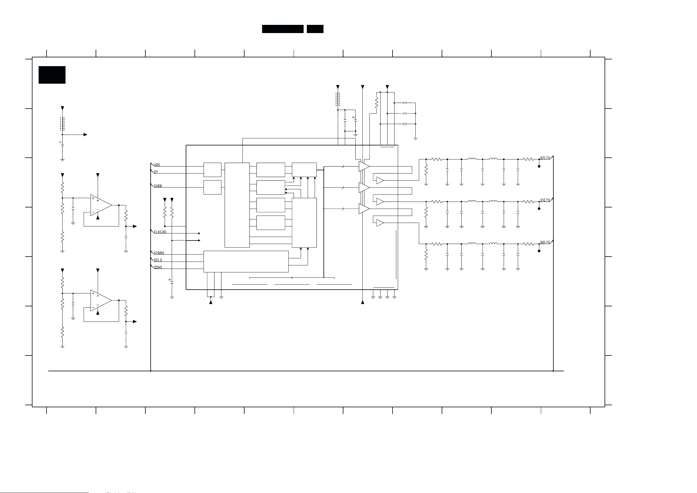
06645003_001.eps
280400
Clock
driver
D8
Clock
driver
D9
Clock
driver
D10
Sub-sampling
R
D5
Sub-sampling
G
D6
Gamma
RDA
GDA
BDA
HD
DY
CLK
D1
I/O
expanders
D3
Uniformity
correction
D2
D7
Sub-sampling
B
LCD
R
LCD
R
LCD
R
Clock generation
D4
I2C
LC4242/4246 5-4 5-5 LC4242/4246
PCS 106 576 PCS 106 577

Block diagrams
OUTR
18
IC7004
ET5020
GAMMA
BIAS
21
22
+8
RDA
B10
B8
B6
7006
24
GDA
26
BDA
U181
27
50
GAMMA
SET
OUTG
16
OUTB
14
17
5V
8
7
SDA5SCL
EAROM
6
06645003_002.eps
280400
D1
D5
D5
D6
9241
9242
9243
9185
9194
9195
9196
9197
9196
9184
9183
V33
Output
I/F
I2C
POS1
POS2
DIRXRB
DIRX6G
30 ET5
31 ET5
32 ET5
SCL
SDA
VD
HD
CKDI
D7
D7
D2
DLYG
3
D6
WP2
15
32
3092
3070
31 30
51 52
SCL SDA
19
4
A4
B4
D6
D8
D10
-5
+5
+8
+15
D1
C1
B1
A1
32ETS
7100
CDX3503R
7102A
LM358D
VRH
31ETS
30ETS
+5
+5
+5
34
06645003_003.eps
280400
D2
D1
9171
9170
9173
HD0
DY
DXRR
STRBS
SCLS
SDAS
CLKCXD
D4
D4
17
7102B
LM358D
VRL
mem
R
Serial
Interface
memGmem
B
Main
Controller
Uniformaty
Correction
D
A
D
A
D
A
HIV
detect
HST
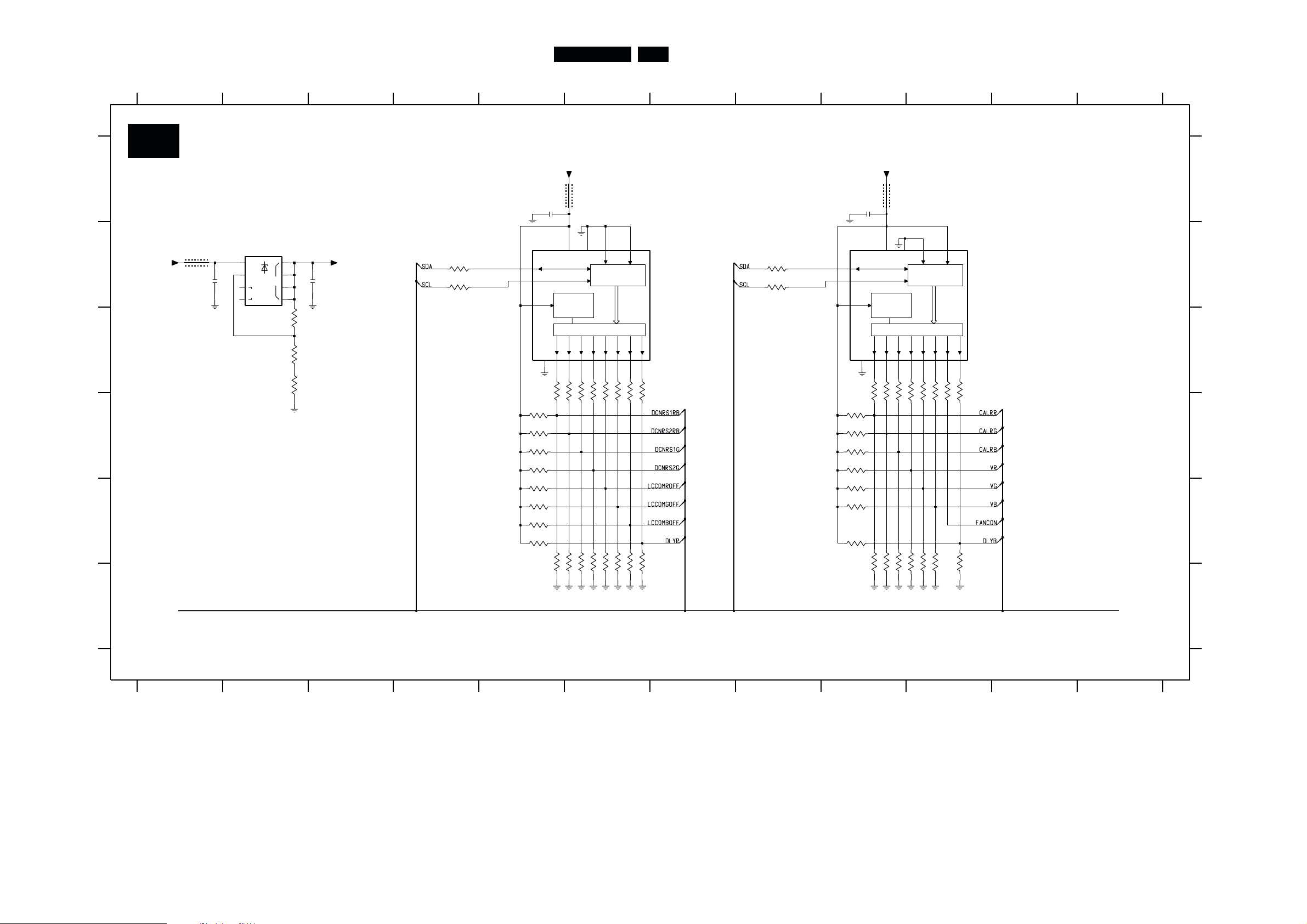
DCNRS1RB
9
7202
TDA8444T
7200
LM3172
D
A
17
5
6
+12V+15V
SCL
SDA
4
3
DCNRS2RB
10
DCNRS1G
11
DCNRS2G
12
LCCOMROFF
13
LCCOMGOFF
14
LCCOMBOFF
15
DLYR
16
I2C
06645003_004.eps
190400
CALRR
9
7204
TDA8444T
D
A
1
+15V
4
3
CALRG
10
CALRB
11
VR
12
VG
13
VB
14
FANCON
15
DLYB
16
I2C
5
6
7
D3
LC4242/4246 5-6 5-7 LC4242/4246
PCS 106 578 PCS 106 579

Block diagrams
FRP
56
7318
ET2081F0A
Clock
gen
1
78
3V3 5V
5V
HD0
7300
7304
77
VD0
9
7346-7354
CKDWS
CLXBB
58
DXBB
57
CLXGG
56
DXGG
55
CLXRR
54
DXRR
53
CLY
52
DY
51
61 21
5V
65
06645003_005.eps
280400
D4
D8
D9
D10
9265
ENB2BB
48
Timing
gen
Serial
ENB1BB
47
ENB2GG
46
ENB1GG
45
ENB2RR
44
ENB1RR
43
D8
D8
D10
D2
D9
STRB10
7302
PCF8574TS
I
O
DATA
SCL
SDA
11
CLK12
SDAS
17
SCLS
19
STRBS
20
60
73 74 75
20 40
15
+15V
42
7402
ET6050SOB
33
34
(to lcd)
LCCOMR
LCCOMROFF
49
50
45
53
23
51
44
CALRR
35
VR
7400
ET6050SOB
36
FRP
46
V33
47
OUTR
VIDR 3
VIDR 5
VIDR 1
To the
LCD
VIDR 7
VIDR 9
VIDR 11
32
30
28
21
19
17
D5-6-7
LC
com
SH1
Vref inverter
Polarity
inverter
58
MCLKR
54
DLYR
Clock
2
CLP
11
SHFNB
5
POS1
6
POS2
14 52
DIRXRB
+5V
SH2
SH3
SH4
SH5
SH6
Timing gen
9145
44
51
VIDR 4
VIDR 6
VIDR 2
VIDR 8
VIDR 10
VIDR 12
32
30
28
21
19
17
06645003_006.eps
280400
SH1
58
MCLKR
54
DLYR
Clock
2
CLP
11
SHFNB
5
POS1
6
POS214DIRXRB
SH2
SH3
SH4
SH5
SH6
Timing gen
+5V
52
+15V
VINR
CALR
42
20 40
HRS2R
44
7708
ET1021FOA
NRS
level shifter
80
+5
HRS1R
43
64
+5
06645003_008.eps
280400
D8-9-10
9003
9006
Clock
level shifter
&
Inverter
ENB1R
36
DXR
27
NRGR
37
ENB2R
35
CLXRIR
30
DXR
32
CLXR
31
DYR
27
DIRYR
38
CLYR
29
CLYNR
28
ENB1RR
18
DIRXRB
19
NRG
16
ENB2RR
17
FRP
78
DCNRS2RB
67
DCNRS1RB
68
CLXRR
11
DY
14
DIRY
15
DXRR
12
CLY
13
42 40
To the
LCD
7700-7704
7710-7714
86645003_007.cdr
250400
Control
Supply Lamp
Lamp is on
Start
to SSB
3
2
1
Flag
SCI
1
2
CBIC81
+300V
Lamp supply board
to PSB
86645003_019.cdr
250400
POWER SUPPLY BOARD
K4
K1
To lamp
supply
panel
To interconnect
board
100250V
AC
2
1
2
1
3
10
13
15
11
8-9
5
1
Auto-
voltage
+295V
+295V
+5 STBY
+15V6
+14V
+8V1
+5V1
-5V0
POW-ON
Standby
supply
Main
supply
K3
LC4242/4246 5-8 5-9 LC4242/4246
PCS 106 580 PCS 106 581

Wiring diagram
wiring.cdr
CL 261000
LC4242/4246 5-10
PCS 106 582

Oscillograms
ITEM 9003
ITEM 9006
ITEM 9069
ITEM 9075
ITEM 9101
ITEM 9106
ITEM 9135
ITEM 9140
ITEM 9145
ITEM 9170 ITEM 9190 ITEM 9233 ITEM 9905
ITEM 9171
ITEM 9173
ITEM 9180
ITEM 9183
ITEM 9184
ITEM 9185
ITEM 9191
ITEM 9193
ITEM 9194
ITEM 9195
ITEM 9196
ITEM 9197
ITEM 9241
ITEM 9242
ITEM 9243
ITEM 9265
ITEM 9901
ITEM 9903
ITEM 9907
OSC_1.CDR
261000
LC4242/4246 5-11
PCS 106 583

6. Diagrams & PWB layouts
OUTPUT
I/F
BUS
CLAMP
CLAMP
AMP
AMP
DRIVER
DRIVER
CLAMP
INPUT
I/F
I2C
CLAMP AMP DRIVER
V-CTRL
-AMP-ADJUST
DAC / CONTROL
ADDRESS 76 HEX
1 2 3 4 5 6 7 8 9 10 11 12 13
1 2 3 4 5 6 7 8 9 10 11 12 13
A
B
C
D
E
F
G
H
A
B
C
D
E
F
G
H
1000-1 B1
1000-2 D1
1000-3 F1
1000-4 B3
1000-5 D3
1000-6 F3
1000-7 B5
2000 B10
2002 B11
2004 B10
2006 B12
2008 C9
2010 C9
2012 C9
2014 C9
2016 D6
2018 D6
2020 D6
2022 D7
2024 D9
2026 D9
2028 D9
2030 D12
2032 D12
2034 D9
2036 E9
2038 E9
2040 E9
2042 E9
2044 E6
2046 E9
2048 E9
2050 E9
2052 F9
2054 F9
2056 F9
2058 F9
2060 F6
2062 F9
2064 F9
2066 F9
2068 G9
2070 G9
2072 G9
2074 G5
2076 G6
2078 G9
2080 G9
2082 E8
2084 E8
2086 E8
3000 B9
3002 B11
3004 B9
3006 C12
3008 C2
3010 C3
3012 C3
3014 C9
3016 C4
3018 C3
3020 D4
3022 D12
3024 D3
3026 D4
3028 D6
3030 D3
3032 D2
3034 E6
3036 E6
3038 E2
3040 E3
3042 E6
3044 E2
3046 F6
3048 F2
3050 G6
3052 G5
3054 G7
3056 G9
3058 G9
3060 B9
3062 C12
3064 D3
3066 E3
3068 E3
3070 A13
3071 A13
3072 A13
3073 A13
3074 A13
3075 B13
3076 B13
3077 B13
3078 B13
3079 B13
3080 D12
3081 D12
3082 E13
3083 E13
3084 E13
3085 E13
3086 F13
3087 F13
3088 F13
3089 F13
3090 F13
3091 F13
3092 F13
3093 G13
3094 G13
3095 G13
3096 G13
3097 G13
3098 G13
3099 G13
3911 C13
3912 C13
3913 C13
3914 C13
3915 C13
3916 C13
3917 C13
3918 D13
3919 D13
3920 D13
3921 D13
3922 D13
3923 D13
3924 D13
3925 E13
3926 E13
3927 E13
3928 B13
3928 H13
3929 B13
5000 B11
5002 B5
5004 B5
5006 B5
5008 C5
5010 F6
5012 C5
5014 C5
6000 B9
7000 D6
7004 B10
7006 E6
7008 F6
7010 E6
9180 C2
9183 E2
9184 E2
9185 F2
9186 F2
9190 C3
9191 C3
9193 D3
9194 B7
9195 B7
9196 B7
9197 C7
9199 C3
9233 E2
9236 F2
9241 C12
9242 C12
9243 C12
3K33928
3K3
3099 3K9
3K93097
3098
3095 3K9
3K33096
10K3093
3094 4K7
3091 10K
4K73092
3089
3090
4K7
3K33088
10K
3086 3K3
3087 3K9
3K33084
3K93085
9199
3083 3K9
9186
3082 2K7
3926 2K7
6K83927
3924 2K7
3925 6K8
3923 6K8
10K3921
3922 1K5
10K3919
3920 1K5
10K3917
3918 1K5
3916 3K3
3914 3K3
3K93915
3912 3K3
3K93913
3K93911
3075
1K5
1K5
3073
8K23074
3072 8K2
3071
1K5
5014
BLM21
8K23070
47u
2018
BLM21
5012
47u
2016
9242
9243
9197
9241
9195
9196
9194
9191
9193
9236
9190
9184
9185
9233
9183
9180
U237
100p
2044
2002
22u
2022
10u
2020
33u
U186
U180
WC_
7
REF
7008
ST24E16
E0
1
E1
2
E2
3
SCL
6
SDA
5
VCC
8
VSS
4
TL431
7006
2A367
1
C
4
NC
5
8
+15V
3046
4K7
+15VGE
+15VGE
+5V
+8V
-5VGE
-5VGE
+5VGE
+8VGE
8V33
21
VCC
+5V
+8VGE
+5VGE
16GOUT
5INV-CNT
15
PGND
1POS-CNT1
2POS-CNT2
17
PVCC
22 RIN 18ROUT
51 SCL
52 SDA
9TESTIN1
10TESTIN2
11TESTIN3
6TESTOUT1
7TESTOUT2
GAMG-B1G
37 GAMG-B1P
49 GAMG-B2G
40 GAMG-B2P
43 GAMG-WHG
34 GAMG-WHP
13GAMOFF
45 GAMR-B1G
36 GAMR-B1P
48 GAMR-B2G
39 GAMR-B2P
42 GAMR-WHG
33 GAMR-WHP
24 GIN
19
GND
23 ATT
26 BIN
12BLKLIM
14BOUT
25 CLPLEV
20 CLPPLS
4DIR-CNT
3DLY-CNT
47 GAMB-B1G
38 GAMB-B1P
GAMB-B2G50
41 GAMB-B2P
44 GAMB-WHG
35 GAMB-WHP
46
+5ST
ET5020S0A
7004
32 AMPBBIAS
29 AMPBGAIN
31 AMPGBIAS
28 AMPGGAIN
30 AMPRBIAS
27 AMPRGAIN
+15VGE
+8VGE
+5ST
-5V
+8V
+5V
-5VGE
100R
3052
+5V
3054
100R
3050
22K
5010
BLM21
100n
2060
3028
1R
1R
3034
7000
BCP56
BCP56
7010
3036
4K7
330R
3042
5006
BLM21
BLM21
5008
BLM21
5004
D2
D3
D4
D5
D6
D7
D8
D9
5002
BLM21
1000-4
106081
D1
D10
D11
2078
100p
100R
3040
100p
2080
22K
3026
3016
3020
22K
100R
3030
22K
100R
3018
3024
100R
3012
100R
Z2
Z3
Z4
Z5
Z6
Z7
Z8
Z9
F5
F6
F7
F8
F9
1000-7
106081
Z1
Z10
Z11
E8
E9
1000-6
106081
F1
F10
F11
F2
F3
F4
1000-5
106081
E1
E10
E11
E2
E3
E4
E5
E6
E7
22K
22K
3048
22K
3038
3044
3032
22K
22K
3008
1000-3
106081
C1
C10
C11
C2
C3
C4
C5
C6
C7
C8
C9
B1
B10
B11
B2
B3
B4
B5
B6
B7
B8
B9
A2
A3
A4
A5
A6
A7
A8
A9
1000-2
106081
1000-1
106081
A1
A10
A11
3004
12K
3058 100R
6000
BAV99
3000
100R3056
10n2014
8K2
4K7
3002
10n
2006
10K
3006
1R
3062
100n
2004
10n
2032
2030
10n
5000
2000
100n
1R
3060
BLM21
2012 100n
10n2072
2070 10n
10n2068
2066 10n
10n2064
2062 10n
10n2058
10n2054
2056 10n
2052 10n
10n2050
2048 10n
10n2046
2042 10n
10n2040
2038 10n
10n2036
2034 10n
2028 10n
10n2026
100n2010
2024 10n
2008 100n
{BDA,GDA,RDA,CLPPLS,OUTR,OUTG,OUTB,DLYR,DLYG,DLYB,POS1,POS2,DIRXRB,DIRXGG,SCL,SDA,V33,VD,HD,CKDI,WP2,FANCON,30ET5,31ET5,32ET5,SCLS,SDAS,STRBS,STRB}
D1.eps
CL 110400
D1
LC4242/4246 6-1
PCS 106 584
LC4242/4246 6-2
ELIM
50 50 5
DOUT1 DOUT2
BUFF.
MEMORY
(SRAM)
DAC
DAC
6 bit
6 bit
CONTROLLER
MAIN
DETECT
SERIAL I/F BLOCK
MASTER CLOCK
SYSTEM CLEAR
H, V
DAC
6 bit
DVSS
DVDD
NC
MAIN
BUFF.
COUNTER
H UP/DOWN
COUNTER
V UP/DOWN
BLOCK
OPERATION
CONTROLLER
MEMORY
0
DOUT0
MEMORY
(SRAM)
1 2 3 4 5 6 7 8 9 10 11
1 2 3 4 5 6 7 8 9 10 11
A
B
C
D
E
F
G
A
B
C
D
E
F
G
2100 A8
2102 B8
2106 C9
2108 B1
2112 D9
2116 D9
2118 D1
2120 D9
2122 D10
2124 C9
2126 C10
2128 E1
2130 E3
2132 B8
2134 D9
2136 D10
2138 B7
2140 B6
2142 C10
2144 D10
2146 D10
2148 C9
2150 D9
2152 D9
2154 D2
2156 F2
3116 C1
3120 D1
3122 C8
3124 C10
3126 D1
3128 D2
3130 B8
3132 B10
3134 F2
3136 E1
3138 D3
3140 E1
3142 D8
3144 D10
3146 B7
3150 F1
3152 D3
3154 E3
3156 E3
3158 D3
3160 A7
3162 C8
3164 D8
3166 D8
5104 B1
5114 C9
5116 C10
5118 B9
5120 B10
5122 D9
5124 D10
5126 A6
7100 B3
7102-A C2
7102-B E2
9170 D10
9171 C10
9173 E10
1K1K
3166
1K
31623164
+5ST
-5V
-5V
1u
2156
5
6
7
8
4
3134
10R
1u
VRL
LM358D
7102-B
10R
3128
2154
7102-A
LM358D
3
2
1
8
4
VRH
+5ST
220p
21502152
220p
2148
220p
+5V
1R3158
470p
21422144
470p
9173
470p
2146
9171
9170
2116
1n
2106
1n1n
2112
+5VCXD
3138 10K
+5V
100n
2140
15u2130
BLM21
5126
+5V
100n
100n
2102
VRH
100n
2100
2132
+5VCXD
1R
3160
3n3
2134
2136
4n7
33u
5124
3144
1K
5122
27u
3142
100R
2124
3n3
4n7
2126
1K
3132
27u
5118 5120
33u
100R
3130
2122
4n7
3124
1K
3n3
2120
33u
5116
3122
100R
5114
27u
47u
2108
+5VCXD
BLM21
5104
3150
1K8
+5V
10K
3140 3136
10K
2128
1u 1u
2118
+5ST
1K5
3126
10K
31163120
15K
VRL
+5ST
40
3 VST
61 XCLR
2138
47u
52
53
54
55
33
OLIM
6
RGT
58 SCLK
57 SCTR
59 SDAT
SLCK64
8
TEST0
TEST1
910
TEST2
44
VRHVRL
29 30
243456
17354962
5
DWN
4 HST
60 HSYNC
1
2
50
51
DACO2
11 12 13 14 15 16 18 19 20 21 22 23 25 26 27 28
48AOUT0
43AOUT1
38AOUT2
45
AVDD
39
AVSS
47BFIN0
42BFIN1
37BFIN2
63 CLKI
7
CTRL
31
DACK0
32
DACKI
46DACO0
41DACO1
36
CXD3503R
7100
{HDO,SDAS,SCLS,STRBS,CLKCXD,DY,DXRR,AB,CD,EF,30ET5,31ET5,32ET5,A,B}
{HDO,SDAS,SCLS,STRBS,CLKCXD,DY,DXRR,AB,CD,EF,30ET5,31ET5,32ET5,A,B}
D2.eps
CL 110400
D2
PCS 106 585
LC4242/4246 6-3
DAC0-7
SLAVE RECEIVER
I C BUS
GENERATOR
REFERENCE
VOLTAGE
2
VOUT
NC
DAC0-7
SLAVE RECEIVER
I C BUS
GENERATOR
REFERENCE
VOLTAGE
2
1 2 3 4 5 6 7 8 9 10 11 12
1 2 3 4 5 6 7 8 9 10 11 12
A
B
C
D
E
F
A
B
C
D
E
F
2200 A5
2202 A9
2204 B1
2206 B2
2208 B4
2210 B5
2212 B8
2214 B8
3200 B4
3202 B8
3204 B4
3206 B8
3208 C2
3210 C2
3212 C2
3214 D5
3216 D6
3218 D6
3220 D6
3222 D6
3224 D6
3226 D6
3228 D6
3230 D9
3232 D9
3234 D9
3236 D10
3238 D10
3240 D10
3242 D10
3244 D10
3246 D5
3248 D9
3250 D5
3252 D9
3254 D5
3256 D9
3258 D5
3260 D9
3262 E5
3264 E9
3266 E5
3268 E9
3270 E5
3272 E9
3274 E5
3276 E9
3278 F5
3280 F6
3282 F6
3284 F6
3286 F6
3288 F6
3290 F6
3291 F10
3292 F6
3293 F10
3294 F9
3295 F10
3296 F9
3297 F10
3298 F9
3299 F10
5200 A5
5202 A9
5204 B1
7200 B2
7202 B5
7204 B9
ADDRESS 4C HEX
ADDRESS 48 HEX
39K
3254
3246
39K
56K3240
56K3236
3238 56K
3232 12K
12K3234
12K3295
12K3230
3293 12K
3296 8K2
12K3291
220K
3256
8K2
3260
3252
220K
8K2
3268
3264
8K2
220K
3248
8K23299
+12V
+15V
6K83244
+12V
+12V
3276
18K
2206
1u
BLM21
1u
2204
680R
5204
3210
1K2
3212
4
ADJ
5
8
1
VIN
2
3
6
7
3208
220R
3206
100R
LM317L
7200
100R
3202
3298 8K2
1R3242
8K23294
BLM21
5202
1u
10
DAC111DAC212DAC313DAC414DAC515DAC616DAC7
8
GND
5
NC
4
SCL
3
SDA
2
Vmax
1
Vp
2202
100R
3204
TDA8444T
7204
6
A07A1
9
DAC0
3200
100R
3290 10K
3286 10K
10K3288
27K3284
3292 8K2
3280 27K
8K23282
3278 8K2
3270
220K
18K
3274
3262
220K
220K
3266
12K
3258
3228 6K8
3250
12K
3K33224
3226 3K3
3222 3K3
10K3220
15K
3218
3214
15K
3216 10K
1u
2200
5200
BLM21
12
DAC413DAC514DAC615DAC7
16
GND
8
5
NC
SCL
4
SDA
3
Vmax
2
Vp
1
{DCNRS1RB,DCNRS2RB,DCNRS1G,DCNRS2G,LCCOMROFF,LCCOMGOFF,LCCOMBOFF,CALRR,CALRG,CALRB,VR,VG,VB,FANCON,SDA,SCL,DLYB,DLYR}{DCNRS1RB,DCNRS2RB,DCNRS1G,DCNRS2G,LCCOMROFF,LCCOMGOFF,LCCOMBOFF,CALRR,CALRG,CALRB,VR,VG,VB,FANCON,SDA,SCL,DLYB,DLYR}
7202
TDA8444T
A06A1
7
DAC09DAC110DAC211DAC3
D3.eps
CL 110400
D3
PCS 106 586

LC4242/4246 6-4
EN
G1
1
MUX1~
&
NC
INTERRUPT
LOGIC
LP FILTER
INPUT
FILTER
I2CBUS
CONTROL
POWER-ON
RESET
I/O
PORTS
SHIFT
REGISTER
8 BIT
ADDRESS 42 HEX
1 2 3 4 5 6 7 8 9 10 11 12 13 14 15
1 2 3 4 5 6 7 8 9 10 11 12 13 14 15
A
B
C
D
E
F
G
H
A
B
C
D
E
F
G
H
2300 A2
2302 B2
2304 B10
2306 B10
2308 B2
2310 B10
2312 B5
2314 B5
2316 C9
2318 C5
2320 C11
2322 C12
2324 C13
2326 D2
2328 D12
2330 D13
2332 E3
2334 E13
2338 F9
2340 F11
2342 F5
2344 H10
2346 G6
2348 H8
2350 H4
2352 H8
2354 F15
2356 F1
2358 F2
2360 D11
2362 G15
3302 B7
3303 B7
3304 B7
3305 B7
3306 F7
3307 D9
3308 G7
3309 H10
3310 A13
3311 A13
3312 A13
3313 A13
3314 A13
3315 A14
3316 A14
3317 A14
3318 B14
3319 B14
3320 B14
3321 B10
3322 C15
3323 B10
3324 C15
3325 B1
3326 B2
3327 B4
3328 F1
3329 B4
3330 E4
3331 E4
3332 C2
3333 C9
3334 C9
3335 C4
3336 C9
3337 D4
3338 D9
3339 D4
3340 D9
3341 D1
3342 D2
3343 D4
3344 D4
3345 D5
3346 D9
3347 D9
3348 D9
3349 D9
3350 F1
3351 D4
3352 A14
3353 E9
3354 B14
3355 E9
3356 A15
3357 E9
3358 A15
3359 E9
3360 B14
3361 E9
3362 D10
3363 E9
3364 D11
3365 G15
3374 F7
3377 G5
3378 G5
3379 G6
3380 G11
3382 H7
3383 H8
3384 G8
3386 H6
3387 H4
3388 H6
3390 H4
3392 B7
3394 B7
3396 B7
3398 B7
3399 E1
3930 D10
5300 A10
5302 A1
5304 B2
5306 C12
5308 C13
5310 C10
5312 D2
5314 F10
5316 G4
5318 H8
5907 F14
6300 F11
6302 H11
6304 E1
6306 E1
7300 B1
7302 A11
7304 B2
7306 C2
7308-A C11
7308-B D12
7308-C E12
7308-D E12
7308-E G1
7308-F E3
7310-A C12
7310-B D13
7310-C E13
7310-D E13
7310-E F13
7310-F H1
7312-A C10
7312-B E10
7318 C6
7320 E5
7326 D2
7338-A F10
7338-B H11
7340 G7
7346 H5
7348 H6
7352 H5
7354 H5
7356 F14
9265 C9
9901 D12
9903 E9
9905 G9
9907 G15
100p
100p100p
1R
1R
3365
1R3392
1R3930
3364
9903
3360 1R
9905
3352 1R
1R3354
+3V3EM
U256
7308-F
74LVC04A
4K7
3330
7320
BC847C
3351
1K
3331
4K7
2358
100n
3328 4K7
1R3318
BAT17
6306
1R3320
3319 1R
9901
9265
9907
3399
1K
1R3303
+5VET
3398 1R
1R3396
BAT17
6304
2356
100K3350
22p
+5VET
+5VET
+5VET
+3V3ET
+3V3SW
BLM21
5907
12
15
GND
8
1
VCC
16
100n
2354
2
3
4
5
6
7
11
10
9
14
13
7356
74LVC157A
+3V3SW
10n
2326
3342
4K7
+3V3ETL
BC857C
7306
4K7
3341
+3V3ET
7310-F
74LVCU04A
13
7
14
12
+3V3L
74LVCU04A
7310-E
11
7
14
10
+3V3L
7
14
8
+3V3L
BLM21
74LVCU04A
7310-D
9
+3V3ETL
+3V3L
5308
23302334
2328
+3V3EM
+3V3EM
+3V3EM
74LVC04A
7308-E
11
7
14
10
74LVC04A
7308-D
9
7
14
8
74LVC04A
7308-C
5
7
14
6
74LVC04A
7308-B
3
7
14
4
+3V3EM
BLM21
5306
7308-A
74LVC04A
1
7
14
2
3K3
3332
100n
2346
2332
100n
5312
BLM21
16
VCC
3
5
7
9
11
13
+5V
74HCT365D
7326
2
4
6
10
12
14
8
GND
1
15
+3V3L
7310-C
74LVCU04A
5
7
14
6
+3V3L
7
14
2
7310-B
74LVCU04A
3
7
14
4
74LVCU04A
7310-A
1
100n
2352
2348
100n
2350
100n
U281
U280
U275
BLM21
-5V
47R
3382
5318
1K5
3383
7340
BF840
2K7
3384
2K2
3390
3386
470R
+5VET
470R
3379
100R
33883387
100R
BF840
7354
BF550
7348
3378
47R
+8V
7352
BF840
BLM21
5316
47R
3377
7346
BF550
470R3333
1R
3307
U240
U251
1R
3306
U250
U249
2324
100n
U239
+3V3EM
+3V3ET
100n
2322
3308
2302
33u
3344
1R
1R
1R3343
+5VET
+5VET
+3V3ET
100R3323
3317 4K7
3321 100R
4K73316
4K73314
3315 4K7
3312 4K7
4K73313
4K73311
5300
BLM21
+5V
3310 4K7
100n
2310
81318
P0 10
P1 11
P2 12
P3 14
P4 16
P5 17
P6 19
P7 20
SCL
2
SDA
4
VDD
5
VSS
15
7302
PCF8574TS
A0
6
A1
7
A2
9
INTn
1
3
47u
2300
+5V
+5V
5302
BLM21
+5VET
BLM21
5304
+3V3ETT
7300
BCP56
3325
100R
100p
2308
3326
1K2
67
1
C
4
NC
5
8
REF
TL431
7304
2A3
+5VET
100n
2342
2338
100n
3363 47R
+3V3ETT
3359 47R
47R3361
3355 47R
47R3357
47R3353
3348 47R
47R3349
3346 47R
47R3347
3338 47R
47R3340
47R3336
2316
100n
3334 47R
+5VET
100R
3327
3329
100R
2312
470p
+3V3ETT
47p
2314
2318
100n
3335 1R
+5VET
VSS2-2
40
VSS3
60
VSS4
80
VSS5
77
VSYNC
2
SRESET
76
STAT E
73
STRB
10
TEST1
79
TEST2
21
VCC1-1
49
VCC1-2
61
VCC1-3
1
VCC2-1
4
VMODE1
5
VMODE2
28
VRESET
20
VSS1
32
VSS2
41
9
OSCI
6
PMODE
78
RESET2
8
SETSW
33
SHCLK134SHCLK235SHCLK336SHCLK437SHCLK538SHCLK639SHCLK7
31
SHENB
22
SHENSW25SHSEL
23
SHSW124SHSW2
53
DXOUTR
51
DYOUT
47
ENBX1B
45
ENBX1G
43
ENBX1R
48
ENBX2B
46
ENBX2G
44
ENBX2R
7
EXTSW
3
FHIN
59
FRP
27
HRESET
62
IMODE
42
MSKOUT
50
NRG
26
OFH
19
ADJEP3
68
ADJY0
69
ADJY1
70
ADJY2
71
ADJY3
29
CLP130CLP2
58
CLXOUTB
56
CLXOUTG
54
CLXOUTR
52
CLYOUT
72
CMPOS
74
DATA75DCLK
57
DXOUTB
55
DXOUTG
63
ADJDX0
64
ADJDX1
65
ADJDX2
66
ADJDX3
67
ADJDX4
11
ADJEN0
12
ADJEN1
13
ADJEN2
14
ADJEN3
15
ADJEN4
16
ADJEP0
17
ADJEP1
18
ADJEP2
ET2081F0A
7318
{VDO,HDO,FI,CKDSW,SHENB,CLP,CLPPLS,ENB1RR,ENB2RR,ENB1GG,ENB2GG,ENB1BB,ENB2BB,NRG,DY,CLY,DXRR,CLXRR,DXGG,CLXGG,DXBB,CLXBB,FRP,IMODE,DATA,DCLK,MCLKR,MCLKG,MCLKB,HD,VD,CKDSW,CKDIO,SCL,SDA,EXTSW,STRB,STRBS,SCLS,SDAS,CLKCXD,CKDFR,CKDI,DIRY}
D4.eps
CL 110400
D4
PCS 106 587

LC4242/4246 6-5
SW
SW
GND
SW
NC
CLOCK
PHASE
ADJUST
TIMING SIGNAL GENERATOR
S/H
REF LEVEL SIGNAL
POLARITY INVERSION
VIDEO SIG POLARITY
INVERTING AMP
LCCOM
GEN
NC
NC
NC
NC
NC
S/H S/H
S/H S/H S/H
S/H S/H S/H
S/H S/H S/H
S/H S/H S/H
S/H S/H S/H
SW
SW
SW
SW
SW
SW
GND
SW
NC
CLOCK
PHASE
ADJUST
TIMING SIGNAL GENERATOR
S/H
REF LEVEL SIGNAL
POLARITY INVERSION
VIDEO SIG POLARITY
INVERTING AMP
LCCOM
GEN
NC
NC
NC
NC
NC
S/H S/H
S/H S/H S/H
S/H S/H S/H
S/H S/H S/H
S/H S/H S/H
S/H S/H S/H
SW
SW
SW
SW
RED
1 2 3 4 5 6 7 8 9 10 11
1 2 3 4 5 6 7 8 9 10 11
A
B
C
D
E
F
A
B
C
D
E
F
2400 A2
2402 A3
2404 A7
2406 A8
2408 A2
2410 A3
2412 A3
2414 A4
2416 A7
2418 A8
2420 A8
2422 A9
2424 B10
2426 B7
2428 E2
2430 E7
2432 E2
2434 E7
2436 B6
2438 B10
2440 C1
2442 C6
2444 B9
3406 F7
3410 C7
3412 B6
3414 F1
3416 F1
3418 F7
3420 C1
3422 B7
3424 C6
3426 D7
5400 A2
5402 A3
5404 A7
5406 A8
7400 B2
7402 A7
9145 C10
9145
1R
3422
100R
3424
2442
22p
2440
22p
100R
3420
1u
2438
2436
1u
1R
3426
22u
2400
22u
2404
+15V+5ST+15V+5ST
BLM21
5406
2406
10u
5404
BLM21
10u
2402
5402
BLM21
BLM21
5400
2426
100n
2422
1u
100n
2430
100p
100n
2416
2434
2418
100n
2420
100n
32VO1
VO2 30
28VO3
21VO4
19VO5
17VO6
23
PGND
5 POS1
6 POS2
26
PVDD
SHENB11
35
SIGCNT
10 STATE
TESTIN139
38 TESTIN2
TESTO37
52
VCC42VDD
47
VIDI
45
VIDO46VIDR
44 VIN
31
43
48
61
64
4
7
12
15
18
20
22
27
16OFFCAN16
36
FRP
13 FRQC
8 9 24 25 40 41 56 57
33
LCCOMO
34
LCCOMOFF
54 MCLK
55 MCLK_
3
29
51 CALI
50
CALO49CALR
62 CLKIN
63 CLKIN_
59
CLKO60CLKO_
2 CLP
1 CLPPOL
DGND
53
14 DIR
58 DLY
2414
1u
ET6050S0B
7402
100n
2432
2428
100p
2408
100n
2410
100n 100n
2412
30
VO3 28
VO4 21
VO5 19
VO6 17
POS26
PVDD
26
SHENB11
SIGCNT
35
S TATE10
39 TESTIN1
TESTIN238
37 TESTO
VCC52VDD
42
VIDI
47
VIDO45VIDR
46
VIN44
VO1 32
VO2
31
43
48
61
64
4
7
12
15
18
20
22
27
OFFCAN16 16
PGND
23
POS15
FRQC13
8 9 24 25 40 41 56 57
LCCOMO
33
LCCOMOFF
34
MCLK54
MCLK_55
3
29
CALI51
CALO50CALR
49
CLKIN62
CLKIN_63
CLKO59CLKO_
60
CLP2
CLPPOL1
DGND
53
DIR14
DLY58
FRP
36
7400
ET6050S0B
{OUTR,DLYR,POS1,POS2,DIRXRB,V33,LCCOMROFF,CALRR,VR,FRP,LCCOMR,MCLKR,SHENB,CLP,CALR,VINR}{OUTR,DLYR,POS1,POS2,DIRXRB,V33,LCCOMROFF,CALRR,VR,FRP,LCCOMR,MCLKR,SHENB,CLP,CALR,VINR}
VIDR(1:12)
D5.eps
CL 120400
D5
PCS 106 588

LC4242/4246 6-6
SW
SW
GND
SW
NC
CLOCK
PHASE
ADJUST
TIMING SIGNAL GENERATOR
S/H
REF LEVEL SIGNAL
POLARITY INVERSION
VIDEO SIG POLARITY
INVERTING AMP
LCCOM
GEN
NC
NC
NC
NC
NC
S/H S/H
S/H S/H S/H
S/H S/H S/H
S/H S/H S/H
S/H S/H S/H
S/H S/H S/H
SW
SW
SW
SW
SW
SW
GND
SW
NC
CLOCK
PHASE
ADJUST
TIMING SIGNAL GENERATOR
S/H
REF LEVEL SIGNAL
POLARITY INVERSION
VIDEO SIG POLARITY
INVERTING AMP
LCCOM
GEN
NC
NC
NC
NC
NC
S/H S/H
S/H S/H S/H
S/H S/H S/H
S/H S/H S/H
S/H S/H S/H
S/H S/H S/H
SW
SW
SW
SW
GREEN
1 2 3 4 5 6 7 8 9 10 11
1 2 3 4 5 6 7 8 9 10 11
A
B
C
D
E
F
A
B
C
D
E
F
2500 A2
2502 A3
2504 A7
2506 A8
2508 A2
2510 A3
2512 A3
2514 A4
2516 A7
2518 A8
2520 A8
2522 A9
2524 B10
2526 B7
2528 E2
2530 E7
2532 E2
2534 E7
2536 B6
2538 B10
2540 C1
2542 C6
2544 B10
3500 C6
3502 F1
3504 F1
3506 F7
3508 F7
3510 C7
3512 C1
3514 C7
3516 C6
3518 D7
5500 A2
5502 A3
5504 A7
5506 A8
7500 B2
7502 A7
9140 C10
3514
1R
3516
100R2542
22p
3512
100R
2540
22p
9140
2538
1u
2500
22u
2536
1u
22u
2504
1R
+5ST +15V+5ST
3518
5506
BLM21
+15V
10u
2506
BLM21
5504
BLM21
5502
2502
10u
2526
5500
BLM21
100n
1u
2522
100p
2530
100n
100n
2534
100n
25182516
100n
2520
17
35
S TATE10
39 TESTIN1
TESTIN238
37 TESTO
VCC52VDD
42
VIDI
47
VIDO45VIDR
46
VIN44
VO1 32
30VO2
VO3 28
VO4 21
VO5 19
VO6
64
4
7
12
15
18
20
22
27
OFFCAN16 16
PGND
23
POS15
POS26
PVDD
26
11 SHENB
SIGCNT
25 40 41 56 57
LCCOMO
33
LCCOMOFF
34
MCLK54
MCLK_55
3
29
31
43
48
61
CALR
49
CLKIN62
CLKIN_63
CLKO59CLKO_
60
CLP2
CLPPOL1
53
DGND
DIR14
DLY58
FRP
36
FRQC13
8924
7502
ET6050S0B
CALI51
CALO
50
1u
2514
100p
2528
100n
2508
2532
100n
2512
100n100n
2510
TESTIN139
38 TESTIN2
TESTO37
52
VCC42VDD
47
VIDI
45
VIDO46VIDR
44 VIN
32VO1
30VO2
28VO3
21VO4
19VO5
17VO6
4
7
12
15
18
20
22
27
16OFFCAN16
23
PGND
5 POS1
6 POS2
26
PVDD
11 SHENB
35
SIGCNT
10 STATE
41 56 57
33
LCCOMO
34
LCCOMOFF
54 MCLK
55 MCLK_
3
29
31
43
48
61
64
62 CLKIN
63 CLKIN_
59
CLKO60CLKO_
2 CLP
1 CLPPOL
53
DGND
14 DIR
58 DLY
36
FRP
13 FRQC
89242540
ET6050S0B
7500
51 CALI
50
CALO49CALR
{V33,FRP,MCLKG,POS1,POS2,SHENB,CLP,FRQC,DLYG,VG,OUTG,CALRG,LCCOMG,LCCOMGOFF,VING,CALG,DIRXGG}
{V33,FRP,MCLKG,POS1,POS2,SHENB,CLP,FRQC,DLYG,VG,OUTG,CALRG,LCCOMG,LCCOMGOFF,VING,CALG,DIRXGG}
VIDG(1:12)
D6.eps
CL 120400
D6
PCS 106 589
 Loading...