

Page 1
PHILIPS CONSUMER ELECTRONICS
LC04
TECHNICAL TRAINING MANUAL
MMARTIN 01/09/05
Page 2

Table of Contents
Introduction . . . . . . . . . . . . . . . . . . . . . . . . . . . . . . . . . . . . . . . . . .3
Overall Video Signal flow . . . . . . . . . . . . . . . . . . . . . . . . . . . . . . . .5
1fH Signal Processing . . . . . . . . . . . . . . . . . . . . . . . . . . . . . . . . . .7
Comb Filter . . . . . . . . . . . . . . . . . . . . . . . . . . . . . . . . . . . . . . . . . .8
2fH Signal Processing . . . . . . . . . . . . . . . . . . . . . . . . . . . . . . . . . .10
Pixel Plus . . . . . . . . . . . . . . . . . . . . . . . . . . . . . . . . . . . . . . . . . . .11
Sync Processing . . . . . . . . . . . . . . . . . . . . . . . . . . . . . . . . . . . . . .12
Audio Input Processing . . . . . . . . . . . . . . . . . . . . . . . . . . . . . . . . .15
Audio Output . . . . . . . . . . . . . . . . . . . . . . . . . . . . . . . . . . . . . . . . .17
Power On Control . . . . . . . . . . . . . . . . . . . . . . . . . . . . . . . . . . . . .17
Front IR/LED . . . . . . . . . . . . . . . . . . . . . . . . . . . . . . . . . . . . . . . . .19
Board Level Troubleshooting . . . . . . . . . . . . . . . . . . . . . . . . . . . . .25
Service Modes . . . . . . . . . . . . . . . . . . . . . . . . . . . . . . . . . . . . . . . .28
Error Codes . . . . . . . . . . . . . . . . . . . . . . . . . . . . . . . . . . . . . . . . . .36
Abbreviation list . . . . . . . . . . . . . . . . . . . . . . . . . . . . . . . . . . . . . . .38
Page 3
FIGURE 1 - BOARD LOCATIONS
Page 1
Page 4
Page 2
FIGURE 2 - CONNECTOR LOCATIONS
Page 5

INTRODUCTION
The LC04 chassis is an LCD TV chassis designed for the 2004 model year. It is available in
a 17, 23, and 26 inch screen sizes. It has an NTSC TV and FM Radio tuning systems. The
set will display HD via the VGA or HDMI inputs. A Computer can be connected with VGA or
HDMI connector. The set can also tune FM Radio which can be operated alone or while the
set is in the PC mode.
In the following, some of the sets features are listed.
Picture
Wide screen aspect ratio
Pixel resolution 1280 x 768
Progressive Scan
3D Comb filter
Progressive Scan
PIP (Picture in Picture)
Sound
10 watts power output (5 watts per channel)
2 on board flat speakers
Virtual Dolby Surround
Picture modes
4:3
14:9 Zoom
Super wide
Widescreen
Full Screen
Inputs
AV1 Composite/YPbPr(1fh only)
AV2 Composite/SVHS
AV3 Side Connection (Composite/SVHS)
AV4 HDMI: Digital PC/HD
AV5 VGA/RGB/Analog HD YPbPr
Tuning
VHF/UHF/Cable tuning
Stereo FM Radio
The hookup instructions and Quick Use guide are located at the end of the training manual.
Page 3
Page 6
Board Location (Figure 1)
There are eight different in the LC04. These modules are exchanged during field service.
The Power supply panel supplies power to both the LCD panel and the other boards in the
set. This panel is exchange only. No schematic is included in the service manual for this
panel.
The TV/Scaler board contains most of the Video and Audio processing. This board is
repairable to component level.
The Pixel Plus panel enhances the picture before feeding it to the LCD panel.
The Rear I/O panel has the 1Fh Composite, 1Fh Component, HD and PC RGB, Component,
and HDMI inputs.
The Side I/O panel has the Headphone, Composite, and SVHS connections.
The 3D Comb filter panel performs a digital separation of the Composite Video inputs.
Figure 2 shows the connector locations in the set.
Page 4
REAR VIEW -LC04
Page 7
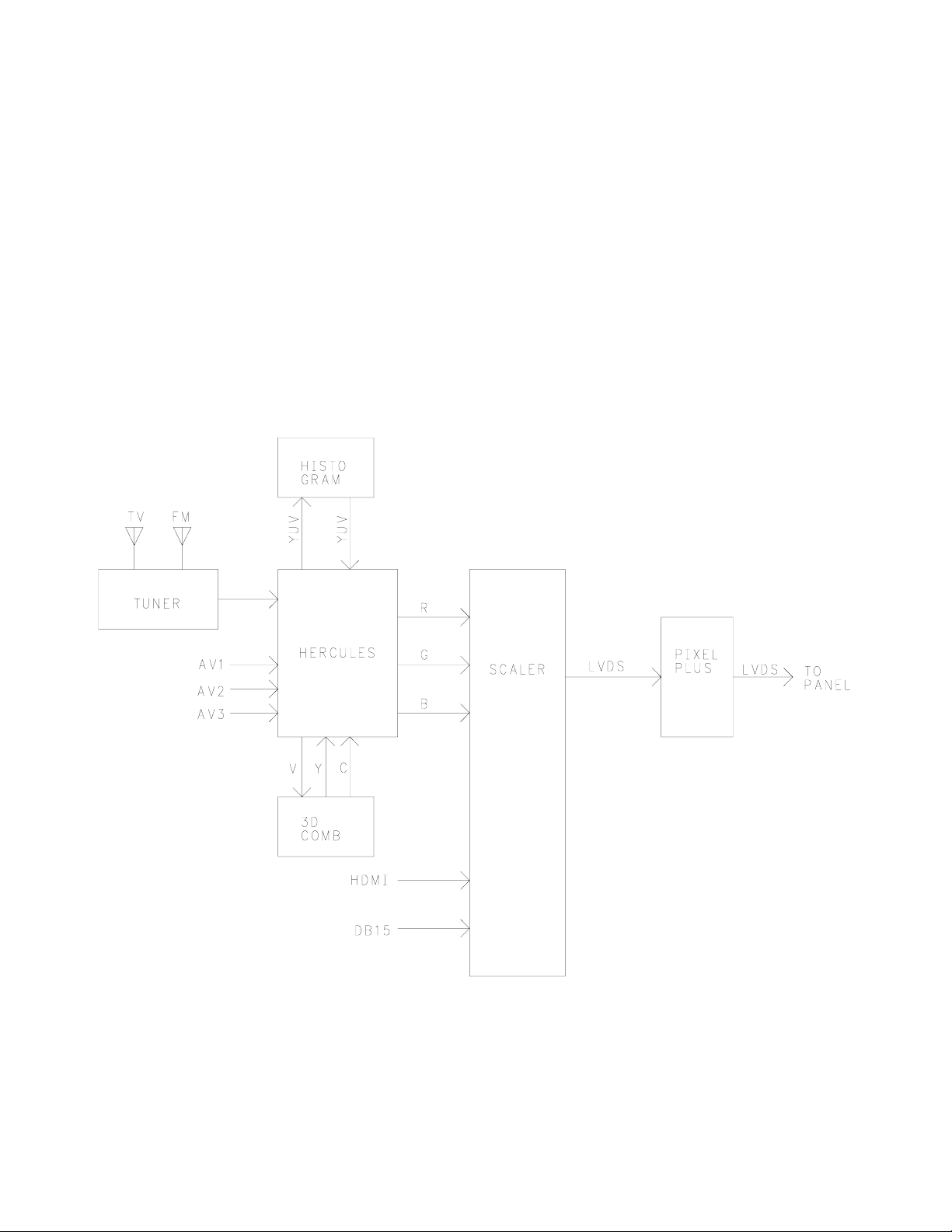
Overall Video signal flow (Figure 3)
There are two large scale IC’s in the LC04. The Hercules chip contains the control interface,
Video processing, and Audio processing. The Hercules also performs TV and FM Radio signal processing. The 3D Comb filter circuit digitally separates and Y and C signal from the
Composite video. The Histogram circuit performs Luminance and Chroma enhancements for
the picture. All of the 1Fh video processing is performed in the Hercules.
The Scaler performs A/D, Digital picture enhancement, and rescaling. All of the 2Fh signal
processing is performed by the Scaler.
The Pixel Plus circuit enhances the picture from the Scaler before feeding it to the LCD
panel.
FIGURE 3 - OVERALL VIDEO SIGNAL FLOW
Page 5
Page 8
Page 6
FIGURE 4 - 1FH SIGNAL PROCESSING
Page 9

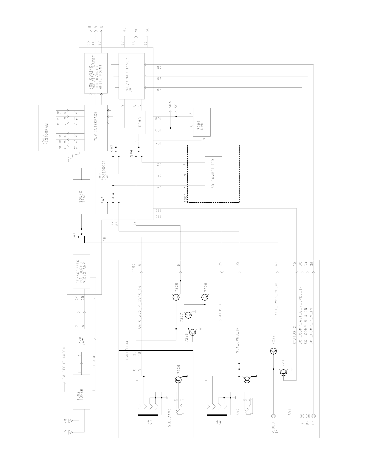
1Fh Signal processing (Figure 4)
The Tuning System in the LC04 can tune both TV and FM Radio frequencies. The set does
not tune ATSC channels.
IF signals from the Tuner, 1302, is output on Pin 11 and fed to the SAW filter, 1328. The signal is then fed to IC 7011, the Hercules chip, on Pins 24 and 25. The output of the
Demodulator is fed to an internal switch, SW1. SW1 selects between the output of the
Demodulator or Composite video from AV1 which is fed to the IC via Pin 48. The selected
signal is then fed to a Sound Trap and to SW2. SW2 selects between the output of the
Sound Trap, AV2, or AV3. If the selected signal on SW2 is Composite video, it is fed to the
3D Comb Filter panel. If the selected signal is Y, it is fed to SW3. SW3 selects the Y signal
from either SW2 or the 3D Comb Filter panel. SW4 selects C from the 3D Comb Filter or
selected C on Pin 59. The STATUS1 line on Pin 116 selects C from AV2 or AV3. If the STATUS1 line is high, Transistor 7226 is turned On, muting AV3. Transistor 7227 is turned Off,
allowing 7225 to pass the C from AV2. If the STATUS1 line is Low, Transistor 7226 is turned
Off, allowing the C from AV3 to pass. Transistor 7227 is turned On in this case, muting the C
from AV2. The Composite inputs on AV2 and AV3 are Mini Jack type connectors.
The output of SW3 is fed to the RGB/YPbPr Insert switch. The C signal is fed to a
Demodulator circuit which then feeds UV to the switch. The Insert Switch selects between
the internal YUV and external YPbPr signal. The YPbPr signal is converted to a YUV signal
in this section. The external YPbPr input can only accept 480i or 1Fh signals. The output of
the switch is fed to a YUV interface circuit. The YUV Interface circuit outputs the signal to
7560, Histogram processing IC. The signal is fed back to 7011 via Pins 70, 71, and 72.
The Signal is then fed to an output circuit. This circuit has fixed Contrast, Brightness, and
White Tone circuits. Closed Caption or Teletext is added to the video in this circuit. OSD is
inserted in the Scaler circuit. RGB drive is output on Pins 85, 86, and 87. This is a 1Fh analog drive signal. Horizontal Sync is output on Pin 67. Vertical Sync is output on Pin 23.
Sandcastle in/out is located on Pin 66.
The Hercules, 7011, also has the Main Microprocessor for the set. The SDA and SCL lines
on Pins 109 and 108 are used to communicate with the rest of the set. IC 7099, NVM, stores
the settings for the Hercules Microprocessor.
The Histogram circuit performs several functions. It improves the Luminance of the picture by
sampling the picture over five amplitude segments. This information is processed to improve
the overall contrast level of the picture. Picture sharpness is improved by sharpening the light
to dark changes in the picture. The Blue stretch circuit detects colors that are near white and
shifts the color more toward blue to give a brighter impression. Skin tone correction is
accomplished by changing the UV mix when colors in the skin tone range are detected.
Page 7
Page 10
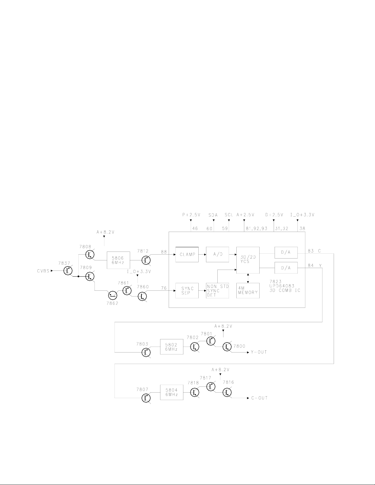
NTSC COMB FILTER CIRCUIT (Figure 5)
The Comb Filter circuit separates the Chrominance and Luminance, YC, from the composite
video. This is a separate PC board that plugs into the System board. The video signal is
amplified by Transistors 703. Transistors 7809, 7862, 7861, and 7860 separate
the Sync from the composite video. The Sync is fed to Pin 76 of 7023. If non-standard Sync
is detected, as with a video game, 7023 performs a 3-line sync separation. The composite
video is buffered by 7808 and fed to a 6MHz filter, 5806. This prevents any high frequency
signals from causing problems with the A/D conversion. The signal from 5806 is buffered by
Transistor 7812 and fed to Pin 88 of 7823. A Clamp circuit sets the sampling range of the
A/D converter. A full frame 3D YC separation is performed by the YCS circuit. The YC signal
is then output to two D/A converters that output C on Pin 83 and Y on Pin 84. The Y signal is
buffered by 7803 before being fed to a 6MHz filter to remove any high frequency components
generated by the D/A conversion. The signal is then buffered by Transistors 7802, 7801, and
7800 before being fed back to the SSB via the System board. A similar circuit also filters the
C signal.
Page 8
FIGURE 5 - 3D COMB FILTER CIRCUIT
Page 11
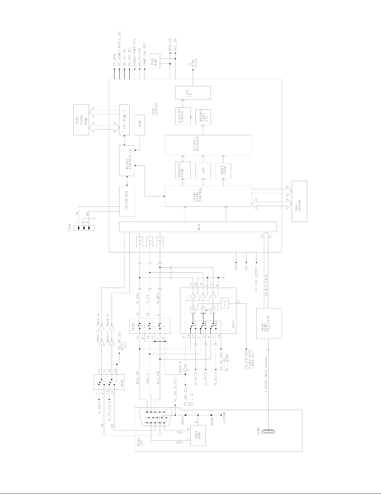
FIGURE 6 - 2fH VIDEO PROCESSING
Page 9
Page 12

2fh Video processing (Figure 6)
The 2Fh section accepts both HD and PC inputs in both analog or digital formats. This section also up-scales the video from the 1Fh section of the TV.
In the HD mode, the set will display:
1080i YPbPr
720p YPbPr
480p YPbPr
This can be input through the VGA or HDMI connectors.
In the PC mode, the set will display:
VGA 640x480 60,72,75,85Hz RGB
VGA 720x400 70,85Hz RGB
VGA 640x350 70,85Hz RGB
MAC 640x480 66.67Hz RGB
MAC 832x624 74.55Hz RGB
SVGA 800x600 56,60,72,75,85Hz RGB
XGA 1024x768 60,70,75,85Hz RGB
WXGA 1280x768 60,75Hz RGB
This can be input through the VGA or HDMI connectors. Inputs using the HDMI connector
must be in an HDMI or DVI digital format.
The DVI connector located on the Rear I/O panel is fed to IC 7808 located on the SSB. IC
7808, the HDMI receiver, detects the TMDS signal and outputs it to the Scaler on 3 8bit data
lines.
The signal on the VGA connector can be either RGB from a computer or YPbPr from an HD
source. If the signal is RGB, the signal is routed to the Scaler via IC 7606, This is controlled
by the PC_HD_SEL line from the Scaler. For PC signals with separate Horizontal and
Vertical sync, the Sync is fed to IC 7605 and then to the Scaler. IC 7605 selected between
the VGA connector and Sync from the Hercules. YPbPr signals from the VGA connector are
fed to IC7607. The input is selected by the Scaler via the SD_HD_SEL line from the Scaler.
This IC has triple Low Pass Filters which clamp the signal before feeding them to the Scaler.
The HD_FILTER line from the Scaler selects between NTSC, if the output of the Hercules is
selected or HD if the VGA connector is selected.
The selected signals are fed to triple A/D converters in the Scaler. The Scaler rescales the
picture as well as performing the Picture in Picture function. An SDRAM IC, 7501, stores the
frames as they are being processed by the Scaler.
The second microprocessor is located in the Scaler. The program for the Scaler is stored IC
7530, Flash Ram. The program can be update via connector 1304 using the ComPair tool.
The Hercules communicates with the Scaler via the SDA and SCL lines.
Page 10
Page 13
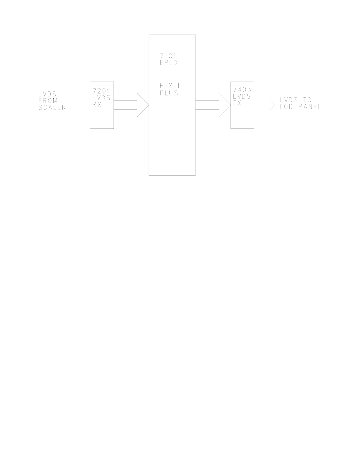
FIGURE 7 - PIXEL PLUS CIRCUIT
Pixel Plus circuit (Figure 7)
The Pixel Plus circuit enhances the video from the Scaler IC. The LVDS output from the
Scaler is decoded by 7202. The signal is then fed to 7101, EPLD, for the Pixel Plus processing. The EPLD provides Color improvement and Sharpness enhancement for the picture.
The 24 bit output of the EPLD is fed to 7403, LVDS Transmitter. The output of 7403 is fed to
the LCD panel.
Page 11
Page 14

Horizontal Sync processing (Figure 8)
The Horizontal Sync from the Hercules is a narrow negative going pulse that is incompatible
with the Scaler. It is necessary to increase the pulse width. The Pulse is fed to Transistor
7018 which inverts the pulse.
The pulse is fed to Pin 2 of 7015. This sets the Latch in the IC causing the Not Q to go Low.
Pin 3 then goes High. Pin 3 will remain High until the voltage on Capacitor 2024 increases to
the point where the Compactor on Pin 6 resets the Latch causing the Not Q to go High,
switching Pin 3 Low.
The Pulse from Transistor 7018 is also fed to 7016. This generates the Horizontal part of the
Sandcastle pulse which is fed back to the Hercules.
Page 12
FIGURE 8 - HORIZONTAL SYNC PROCESSING
Page 15

Vertical Sync Processing (Figure 9)
As with the Horizontal, the Vertical Sync pulse from the Hercules requires processing before
being fed to the Scaler. The Negative Vertical pulse if inverted by Transistor 7019. The
Positive pulse is fed to Pin 2 of 7017 which sets the latch, causing Pin 3 of 7017 to go High.
It will stay High until Capacitor 2034 charges to the point where the Compactor connected to
Pin 6 resets the latch causing Pin 3 to go Low.
FIGURE 9 - VERTICAL SYNC PROCESSING
Page 13
Page 16

Page 14
FIGURE 10 - AUDIO INPUT PROCESSING
Page 17

Audio Input Processing (Figure 10)
All of the audio processing is performed in the Hercules. The Audio processing section of the
Hercules is controlled by the internal microprocessor of the chip. Audio can be input via the
Tuner, the HDMI receiver, or from one of four AV inputs. With the existing software in this set
when the HDMI input is selected, the HDMI bitstream must include audio.
Baseband and IF audio from the Tuner is buffered by 7316. The signal then splits with the
FM signal being fed to Pin 33 of 7011. TV audio is fed to the 4.5Mhz bandpass filter before
being fed to Pin 44.
Audio Data, Word Select, and Clock from the HDMI receiver is fed to 7809, Audio DAC. Left
and Right channel audio from 7809 is fed to switch 7810. When the set is in the PC mode
and the signal source is the HDMI input, the audio can be connected to the PC Audio In jack.
This is a miniature audio jack. Switch 7810 is controlled by the PC_HDMI_AUDIO_SEL line
from the Scaler. In the HD mode, only the 7809, DAC, is selected by the software. For audio
to be present, the HDMI bitstream must contain audio. Audio from AV1, AV2, and Side AV3
are fed directly to the 7011.
The following are available in the TV audio menu:
Equalizer
Balance
Dolby Virtual Dolby/Stereo
SAP
Sound Mono/Stereo
The graphic Equalizer adjust the frequencies of the Left and Right channels over five bands.
The gain of each band is adjustable from -12dB to +12dB in steps of 1dB. Virtual Dolby gives
a surround sound impression with the use of two speakers. The SAP selections selects the
Second Audio Program if available. This selection cannot be made if the an SAP channel is
not available.
Volume control is performed in 7011. The MON_OUT or Monitor out is not used in the LC04.
The only audio output from 7011, Hercules, is the MAIN_OUT.
Page 15
Page 18

Page 16
FIGURE 11 - AUDIO OUTPUT
Page 19

Audio Output (Figure 11)
The audio output has a power amplifier with a 10 watt per channel output. The Power
Amplifier is muted when headphones are connected.
When the set is turned On, the Standby line goes High causing Pin 8 of 7706 to go High.
Transistor 7703-1 turns Off. Capacitor 2703 charges to delay the turn on of 7709 preventing
poping noise in the audio. When the voltage on Pin 12 of 7709 reaches 1.8 volts, the IC
turns On. When 2703 is fully charged, Pin 12 will read 4.5 volts. The Power Down and
Sound-Enable lines will go High turning 7703-2 Off. This signal is fed to the switch in the
Headphone Jack and then to Pin 13 of 7709. Left and Right audio drive from the Hercules is
fed to Pins 14 and 7 of 7709. When headphones are plugged into the side jack panel, the
Mute line on Pin 13 of 7709 will go Low muting the speakers. The audio is routed to the
Headphone amplifier, 7740 and then to the jack on the Side Jack panel. To prevent a Pop in
the Headphones when the set powers down a muting circuit is provided. If the
POWER_DOWN or the EXT_MUTE lines should go Low, Pin 11 of 7706 would go Low,
switching Transistor 7710 Off. Transistors 7708-2 and 7708-1 would be turned On via current
flow through resistor 3730 muting the headphone drive.
Power Control (Figure 12)
The LEDs and IR sensor are located on the Front IR panel. The Keyboard is located on the
Side I/O panel. This is a resistor ladder that causes a voltage change on Pin 120 of the
Hercules when one of the keys are pressed. The Keyboard line will read approximately 3.3
volts when no keys are pressed.
IC 7011, Hercules, contains the main Microprocessor for the set as well as the Video and
Audio processing circuits. The Microprocessor communicates with the rest of the set via the
Standby, Status1, Status2 and I2C bus(SDA and SCL). The IC is powered by the +3V3STBY,
+5VSW, and the +8VSW supplies.
Transistors 7001 and 7003 along with other components not shown provide two 1.8 volt supplies to the Hercules. During Reset, the 1V8B supply is muted. Refer to Figure 12A for a
complete circuit description.
Page 17
Page 20

Page 18
FIGURE 12 - POWER CONTROL
Page 21

FIGURE 12A - 1.8 VOLT REGULATOR
Hercules 1.8 volt regulator (Figure 12A)
The signal from Pin 14 of the Hercules controls the regulation of the 1.8 volt A and B
supplies.
During Hercules Reset, Transistor 7070 turns
On, pulling the 1V8_B supply to ground.
Transistor 7005 grounds the drive to the
1V8_B regulator circuit.
Front IR/LED (Figure 13)
The set has a two color LED. The
PC_TV_LED and LED_SEL lines determine
the color. A light sensor senses the ambient
light in the room and adjust the Brightness
according.
FIGURE 13 - FRONT IR/LED
Page 19
Page 22

Page 20
FIGURE 14 - TV SUPPLY
Page 23

TV Supply (Figure 14)
Connector 1910 connects the SSB to the power supply. The Power Supply board is replaceable as a board and is not repairable. The 3V3STBY supply is the only voltage present when
power is applied to the set when it is turned Off. The Standby line switches High to turn the
set On. The LAMP_ON_OFF signal turns the backlight of the LCD panel On. The 12VUNREG voltage passes through a coil located on diagram A14 to become +12VSW supplying
voltage to 7930.
IC 7930 has two functions. Switched voltage is output on Pin2 and filtered by coil 5931 and
capacitor 2933 to produce the +5VSW supply. The switching voltage from Pin 2 also drives
Transistor 7910, a boost regulator, to produce the +VTUN voltage for the tuner. The +12VSW
supply also feeds regulator 7920 to produce the +8VSW_TV supply.
FIGURE 15 - SUPPLY FROM TV BOARD
Supply from TV board (Figure 15)
This part of the diagram is located on A14. This shows coil 5958 where the +12VUNREG
supply becomes the +12VSW supply.
Page 21
Page 24

FIGURE 16 - PANEL SUPPLY
Panel supply (Figure 16)
When the set is turned On, the Scaler will send the PANEL_PWR_CTL line High turning transistor 7955 On. This turns transistor 7954 On, supplying power to the 12 volt regulator 7953.
This voltage is then fed to the LCD panel via the Pixel Plus panel.
Page 22
Page 25

FIGURE 17 - +5VSW REGULATOR
Figure 17 shows the +5VSW Regulator. This diagram is located on A14.
Figure 18 shows the regulator and filter
circuits for the Scaler IC.
FIGURE 18
Page 23
Page 26

Page 24
FIGURE 19 - PIXEL PLUS REGULATORS
Page 27

Pixel Plus Regulators (Figure 19)
Power and control to the Pixel Plus panel is provided via connector 1001. SDA and SCL is
connected to the panel on Pins 1 and 3. The 5 volt supply is connected to Pin 9. The 5 volt
supply turns Transistor 7505 On, switching 7504 On. This switches the +3V3 supply to the
panel. The 3V3 supply is also supplied to the 1.5 volt regulator 7501.
Board Level Troubleshooting (Figures 20 and 21)
When power is supplied to the set, the only voltage present is the +3V3STBY. This voltage
can be checked on Pins 3 and 4 of connector 1910 on the SSB. When the set is turned On,
Microprocessor on the SSB will switch the Standby line High (3.3V). The BU_LIGHT_ADJ
and LAMP_ON_OFF are switched High when the set is turned On. If the 3.3 volt standby
supply is not present, the power supply panel should be replaced. When the Standby line
goes High, the two 12 volt supplies on Pins 1 and 8 should turn On. If they are not present,
the Power Supply panel should be replaced.
If the sets turns On with the LCD panel not turning On, check the 24 volt supply to the LCD
panel inverter. If this voltage is not present, the Power Supply should be replaced.
Aux and HDMI inputs from the I/O panel can be checked on connectors 1005, 1601, and
1690.
3D Comb filter in/out can be checked on connector 1004. If an oscilloscope is not available,
Pins 3 and 8 can be jumpered to check if the Comb filter is the problem.
All of the audio processing is performed on the SSB. The Speakers are connected to connector 1704.
Referring to Figure 21, the signals to and from the Rear I/O, Side I/O, and Front IR/LED can
be checked.
Page 25
Page 28

Page 26
FIGURE 20 - WIRING INTERCONNECT PART 1
Page 29

FIGURE 21 - WIRING INTERCONNECT PART 2
Page 27
Page 30

Service Modes, Error Codes, and Fault Finding
Test Points
Service Modes
Problems and Solving Tips (related to CSM)
ComPair
Error Codes
The Blinking LED Procedure
Fault Finding and Repair Tips
Power Supply
Service Modes
Service Default mode (SDM) and Service Alignment Mode (SAM) offers several features for
the service technician, while the Customer Service Mode (CSM) is used for communication
between the call centre and the customer.
This chassis also offers the option of using ComPair, a hardware interface between a computer and the TV chassis. It offers the abilities of structured troubleshooting, error code reading,
and software version readout for all chassis.
Minimum requirements for ComPair: a Pentium processor, a Windows OS, and a CD-ROM
drive (see also paragraph 'ComPair').
Service Default Mode (SDM)
Purpose
To create a predefined setting for measurements to be made.
To override software protections.
To start the blinking LED procedure.
To inspect the error buffer.
To check the life timer.
Page 28
Page 31

The Service Default mode sets the set in the following condition
Tuning frequency: 61.25 MHz (Channel 3).
All picture settings at 50% (brightness, colour contrast, hue).
Bass, treble and balance at 50 %; volume at 25 %.
All service-unfriendly modes (if present) are disabled. The service unfriendly modes are:
Timer / Sleep timer.
Child / parental lock.
Blue mute.
Hotel / hospital mode.
Auto shut off (when no “IDENT” video signal is received for 15 minutes).
Skipping of non-favorite presets / channels.
Auto-storage of personal presets.
Auto user menu time-out.
Auto Volume Levelling (AVL).
How to enter
To enter SDM, use one of the following methods:
Press the following key sequence on the remote control transmitter: “062596” directly followed by the MENU button (do not allow the display to time out between entries while keying
the sequence).
Short 'Service' jumpers on the TV board during cold start and apply mains (see Figure
'Service jumpers'). Then press the mains button (remove the short after start-up). Caution :
Entering SDM by shorting 'Service' jumpers will override the +8V-protection. Do this only for a
short period. When doing this, the service-technician must know exactly what he is doing, as
it could damage the television set.
After entering SDM, the following screen is visible, with SDM in the upper right corner of the
screen to indicate that the television is in Service Default Alignment Mode.
How to navigate
Use one of the following methods:
When you press the MENU button on the remote control, the set will switch on the normal
user menu in the SDM mode.
On the TV, press and hold the VOLUME DOWN and press the CHANNEL DOWN for a few
seconds, to switch from SDM to SAM and reverse.
Page 29
Page 32

How to exit
Switch the set to STANDBY by pressing the 'POWER' button on the remote control transmitter or press the 'POWER' switch on the set.
Service Alignment Mode (SAM)
Purpose
To change option settings. To display / clear the error code buffer. To perform alignments
Specifications
Operation hours counter (maximum five digits displayed).
Software version, Error codes, and Option settings display.
Error buffer clearing.
Option settings.
Software alignments (Tuner, White Tone, & Audio).
NVM Editor.
How to enter
To enter SAM, use one of the following methods:
Press the following key sequence on the remote control transmitter: “062596' directly followed
by the I+/STATUS button (do not allow the display to time out between entries while keying
the sequence).
After entering SAM, the following screen is visible, with SAM in the upper right corner of the
screen to indicate that the television is in Service Alignment Mode.
SAM Menu explanation
LLLLL. This represents the run timer. The run timer counts normal operation hours, but does
not count standby hours.
AAABCD-X.Y/EEEEEE F.GG This is the software identification of the main microprocessor:
A = the project name (LC42).
B = the region: E= Europe, A= Asia Pacific, U= NAFTA, L= LATAM.
C = the software diversity:
Page 30
Page 33

Page 31
Page 34

Europe: T= 1 page TXT, F= Full TXT, V= Voice control.
LATAM and NAFTA: N= Stereo non-dBx, S= Stereo dBx.
Asian Pacific: T= TXT, N= non-TXT, C= NTSC.
ALL regions: M= mono, D= DVD, Q= Mk2.
D = the language cluster number.
X = the main software version number (updated with a major change that is incompatible with
previous versions).
Y = the sub software version number (updated with a minor change that is compatible with
previous versions).
EEEEEE = the scaler sw cluster
F = the main sw version no.
GG = the sub-version no.
SAM. Indication of the Service Alignment Mode.
Error Buffer. Shows all errors detected since the last time the buffer was erased. Five errors
possible.
Option Bytes. Used to set the option bytes. See “Options” in the Alignments section for a
detailed description. Seven codes are possible.
Clear. Erases the contents of the error buffer. Select the CLEAR menu item and press the
MENU RIGHT key. The content of the error buffer is cleared.
Options. Used to set the option bits. See “Options” in the Alignments section for a detailed
description.
AKB. Used to disable (Off) or enable (On) the “black current loop” (AKB= Auto Kine Bias).
Tuner. Used to align the tuner. See “Tuner” in the Alignments section for a detailed description.
White Tone. Used to align the white tone. See “White Tone” in the Alignments section for a
detailed description.
Audio. No audio alignment is necessary for this television set.
NVM Editor. Can be used to change the NVM data in the television set. See table “NVM data”
further on.
Page 32
Page 35

SC NVM Editor. Can be used to edit Scaler NVM.
ComPaIr. Can be used to switch on the television to In System Programming (ISP) mode, for
software uploading via ComPair. Caution: When this mode is selected without ComPair connected, the TV will be blocked. Remove the AC power to reset the TV.
How to navigate
In SAM, select menu items with the MENU UP/DOWN keys on the remote control transmitter.
The selected item will be highlighted. When not all menu items fit on the screen, use the
MENU UP/DOWN keys to display the next / previous menu items.
With the MENU LEFT/RIGHT keys, it is possible to:
Activate the selected menu item.
Change the value of the selected menu item.
Activate the selected submenu.
In SAM, when you press the MENU button twice, the set will switch to the normal user menus
(with the SAM mode still active in the background). To return to the SAM menu press the
MENU or STATUS/EXIT button.
When you press the MENU key in while in a submenu, you will return to the previous menu.
How to store SAM settings
To store the settings changed in SAM mode, leave the top level SAM menu by using the
POWER button on the remote control transmitter or the television set.
How to exit
Switch the set to STANDBY by pressing the power button on the remote control transmitter or
press the 'POWER' switch on the set.
Customer Service Mode (CSM)
The Customer Service Mode shows error codes and information on the TV's operation settings. The call centre can instruct the customer (by telephone) to enter CSM in order to identify the status of the set. This helps the call centre to diagnose problems and failures in the TV
set before making a service call.
The CSM is a read-only mode; therefore, modifications are not possible in this mode.
How to enter
To enter CSM, press the following key sequence on the remote control transmitter: “123654”
Page 33
Page 36

(do not allow the display to time out between entries while keying the sequence).
Upon entering the Customer Service Mode, the following screen will appear:
Menu explanation
Indication of the decimal value of the operation hours counter, Software identification of the
main microprocessor (see 'Service Default or Alignment Mode' for an explanation), and the
service mode (CSM= Customer Service Mode).
Displays the last five errors detected in the error code buffer. Displays the option bytes.
Displays the type number version of the set.
Reserved item for P3C call centers (AKBS stands for Advanced Knowledge Base System).
Indicates the television is receiving an 'IDENT' signal on the selected source. If no 'IDENT' signal is
detected, the display will read 'NOT TUNED'
Displays the detected Audio (e.g. stereo/mono).
Displays the picture setting information. Displays
the sound setting information.
To exit CSM, use one of the following methods:
Press the MENU, STATUS/EXIT, or POWER button on the remote control transmitter.
Press the POWER button on the television set.
Problems and Solving Tips Related to CSM
Picture Problems
Note : The problems described below are all related to the TV settings. The procedures used
to change the value (or status) of the different settings are described.
Picture too dark or too bright
If the picture improves when you press the AUTO PICTURE button on the remote control
transmitter, or the picture improves when you enter the Customer Service Mode, then press
the AUTO PICTURE button on the remote control transmitter repeatedly (if necessary) to
choose PERSONAL picture mode.
Press the MENU button on the remote control transmitter to bring up the normal user menu.
In the normal user menu, use the MENU UP/DOWN keys to highlight the PICTURE sub
menu.
Press the MENU LEFT/RIGHT keys to enter the PICTURE sub menu.
Page 34
Page 37

Use the MENU UP/DOWN keys (if necessary) to select BRIGHTNESS.
Press the MENU LEFT/RIGHT keys to increase or decrease the BRIGHTNESS value.
Use the MENU UP/DOWN keys to select PICTURE.
Press the MENU LEFT/RIGHT keys to increase or decrease the PICTURE value.
Press the MENU button on the remote control transmitter twice to exit the user menu.
The new PERSONAL preference values are automatically stored.
White line around picture elements and text
If the picture improves after you have pressed the AUTO PICTURE button on the remote
control transmitter, press the AUTO PICTURE button on the remote control transmitter
repeatedly (if necessary) to choose PERSONAL picture mode.
Press the MENU button on the remote control transmitter. This brings up the normal user
menu.
In the normal user menu, use the MENU UP/DOWN keys to highlight the PICTURE sub
menu.
Press the MENU LEFT/RIGHT keys to enter the PICTURE sub menu.
Use the MENU UP/DOWN keys to select SHARPNESS.
Press the MENU LEFT key to decrease the SHARPNESS value.
Press the MENU button on the remote control transmitter twice to exit the user menu.
The new PERSONAL preference value is automatically stored.
Snowy picture
Check CSM line 6. If this line reads “Not Tuned”, check the antenna connection.
If the Tuner is defective, line 2 will show an error 10. In this case the SSB should be repaired
or replaced. When repairing, check for a defective tuner.
If the Picture is Black and white, check the color level setting.
Error Code
The error code buffer contains all errors detected since the last time the buffer was erased.
Page 35
Page 38

The buffer is written from left to right. When an error occurs that is not yet in the error code
buffer, it is displayed at the left side and all other errors shift one position to the right.
How To Read The Error Buffer
You can read the error buffer in 3 ways:
On screen via the SAM (if you have a picture). Examples:
ERROR: 0 0 0 0 0 : No errors detected
ERROR: 6 0 0 0 0 : Error code 6 is the last and only detected error
ERROR: 9 6 0 0 0 : Error code 6 was detected first and error code 9 is the last detected
(newest) error
Via the blinking LED procedure (when you have no picture). See “The Blinking LED
Procedure”.
How To Clear The Error Buffer
The error code buffer is cleared by using the CLEAR command in the SAM menu.
If the contents of the error buffer have not changed for 50 hours, the error buffer resets automatically.
Note: If you exit SAM by disconnecting the mains from the television set, the error buffer is
not reset.
Error Codes
In case of non-intermittent faults, write down the errors present in the error buffer and clear
the error buffer before you begin the repair. This ensures that old error codes are no longer
present.
If possible, check the entire contents of the error buffer. In some situations, an error code is
only the result of another error and not the actual cause of the problem (for example, a fault
in the protection detection circuitry can also lead to a protection).
Table: Error code overview
Error Device Error description Check item Diagram
0 Not applicable No Error
1 Not applicable
2 Not applicable
3 Not applicable
4 GM1501 I2C error while communicating with the Genesis Scaler
Page 36
Page 39

and/or Flash-ROM is faulty/empty
5 +5v protection
6 I2C bus General I2C error
7 Not applicable
8 M24C32 I2C error while communicating with the Scaler EEPROM
9 M24C16 I2C error while communicating with the EEPROM
10 Tuner I2C error while communicating with the PLL tuner
11 UPD64083 I2C error while communicating with the 3DYC Combfilter
12 Not applicable
13 SII9993CT I2C error while communicating with the HDMI Decoder
14 K4D263238M Read-write error with the Scaler SDRAM
15 TDA9178T/N1 I2C error while communicating with Histogram
16 EPIC12F I2C error while communicating with EPLD on Pixel Plus
panel
NVM Editor
In some cases, parts of the NVM contents need to be changed. This can be done with the
“NVM Editor” option in SAM mode. With this option single bytes can be changed.
Load default NVM values
In case a blank NVM is placed or when the NVM content is corrupted, default values can be
downloaded into the NVM. After the default values are downloaded it will be possible to start
up and to start aligning the TV set. This is no longer initiated automatically; to initiate the
download the following action has to be performed:
Apply AC power to the TV set.
Short circuit the SDM jumpers (keep short circuited)
Press P+ or Ch+ on the local keyboard (and keep it pressed)
Switch on the TV set via the mains switch
When the set has started up the P+/Ch+ button can be released and the short circuit of the
SDM jumpers can be removed.
The red LED will be on continuously to indicate that the download is initiated (normally when
SDM is activated the red LED will start with the Blinking LED sequence).
Wait +/- 30 Seconds (time needed to download default values to the NVM)
Page 37
Page 40

Result: The set is in SDM, the NVM is loaded with default values and the blinking LED is not
activated (The blinking LED is not activated in this case to show that the download has been
performed), the LED will be on.
Page 38
Page 41

Abbreviation list
Description
1080i 1080 visible lines, interlaced
1080p 1080 visible lines, progressive scan
480i 480 visible lines, interlaced
480p 480 visible lines, progressive scan
ADC A/D Analogue to Digital Converter
AFC Automatic Frequency Control: control signal used to tune to the correct
frequency
AGC Automatic Gain Control: algorithm that controls the video input of the
feature box
AM Amplitude Modulation
AV Audio Video
C-FRONT Chrominance front input
CBA Circuit Board Assembly (or PWB)
ComPair Computer aided rePair
CSM Customer Service Mode
CVBS Composite Video Blanking and Synchronization
CVBS-EXT CVBS signal from external source (VCR, VCD, etc.)
CVBS-INT CVBS signal from Tuner
CVBS-MON CVBS monitor signal
CVBS-TER-OUT CVBS terrestrial out
DAC Digital to Analogue Converter
DFU Directions For Use: owner's manual
DNR Dynamic Noise Reduction
DRAM Dynamic RAM
DSP Digital Signal Processing
DTS Digital Theatre Sound
DVD Digital Video Disc
EEPROM Electrically Erasable and Programmable Read Only Memory
EPLD Electronic Programmable Device
EXT EXTernal (source), entering the set by cinches (jacks)
FBL Fast Blanking: DC signal accompanying RGB signals
FLASH FLASH memory
FM Field Memory / Frequency Modulation
FMR FM Radio
FRC Frame Rate Converter
FRONT-C Front input chrominance (SVHS)
FRONT-DETECT Front input detection
FRONT-Y_CVBS Front input luminance or CVBS (SVHS)
H H_sync to the module
HD High Definition
HDMI High Definition Multimedia Interface
HP HeadPhone
I2C Integrated IC bus
I2S Integrated IC Sound bus
Page 39
Page 42

IC Integrated Circuit
IF Intermediate Frequency
Interlaced Scan mode where two fields are used to form one frame. Each field contains
half the number of the total amount of lines. The fields are written in 'pairs',
causing line flicker.
IR Infra Red
IRQ Interrupt ReQuest
Last Status The settings last chosen by the customer and read and stored in RAM or in the
NVM. They are called at start-up of the set to configure it according the cus-
tomers wishes
LCD Liquid Crystal Display
LED Light Emitting Diode
LINE-DRIVE Line drive signal
LVDS Low Voltage Differential Signalling, data transmission system for high speed
and low EMI communication.
MPEG Motion Pictures Experts Group
NVM Non Volatile Memory: IC containing TV related data (for example, options)
OSD On Screen Display
Progressive Scan Scan mode where all scan lines are displayed in one frame at the same
time, creating a double vertical resolution.
RAM Random Access Memory
RC Remote Control transmitter
RC5 Remote Control system 5, the signal from the remote control receiver
RGB Red, Green, and Blue. The primary colour signals for TV. By mixing
levels of R, G, and B, all colors (Y/C) are reproduced.
RGBHV Red, Green, Blue, Horizontal sync, and Vertical sync
ROM Read Only Memory
SAM Service Alignment Mode
SIF Sound Intermediate Frequency
SC SandCastle: two-level pulse derived from sync signals
SCL CLock Signal on I2C bus
SDA DAta Signal on I2C bus
SDRAM Synchronous DRAM
SIF Sound Intermediate Frequency
STBY STandBY
VGA Video Graphics Array
XTAL Quartz crystal
YPbPr Component video (Y= Luminance, Pb/Pr= Colour difference signals)
Y/C Luminance (Y) and Chrominance (C) signal
Y-OUT Luminance-signal
Page 40
 Loading...