

Page 1
Colour Television Chassis
LC03E
AA
Contents Page Contents Page
1 Technical Specifications, Connections,
and Chassis Overview 2
2 Safety Instructions, Warnings, and Notes 5
3 Directions for Use 6
4 Mechanical Instructions 14
5 Service Modes, Error messages,
and Repair Tips 20
6 Block Diagrams
Block Diagram (Tuner-IF-Video) 27
Block Diagram (TV Control and Inverter Panel) 28
Block Diagram (Scaler Board) 29
I2C-IC’s and Error Codes Overview 30
Powerlines Overview 31
Testpoint Overview TV Board (15”/17”) 32
Mapping Testp. and Waveforms TV Board 33
Testpoint Overview Scaler Board 34
Testpoint Overview TV Board (23”) 35
Wiring Diagram 15 & 17 Inch 36
Wiring Diagram 23 Inch Wide Screen 37
7 Electrical Diagrams and PWB lay-outs Diagram PWB
TV Board: U_Cont (Diagram A1) 38 50-69
TV Board: Mem for 100-pg Txt (Diagram A2) 39 50-69
TV Board: Tuner Function (Diagram A3) 40 50-69
TV Board: IF Video Sync Chr. (Diagram A4) 41 50-69
TV Board: SAW Filter (Diagram A5) 42 50-69
TV Board: Analog Comb Filter (Diagram A6) 43 50-69
TV Board: Audio Delay Line (Diagram A7) 44 50-69
TV Board: Audio Processing (Diagram A8) 45 50-69
TV Board: Audio Ampl. (15”/17”)(Diagram A9a) 46 50-69
TV Board: Audio Amplifier (23”) (Diagram A9b) 47 50-69
TV Board: Local Supply (Diagram A10) 48 50-69
TV Board: SCART I/O (Diagram A11) 49 50-69
Scaler Panel: Power (Diagram C1) 70 80-89
Scaler Panel: I/O & Interface (Diagram C2) 71 80-89
©
Copyright 2003 Philips Consumer Electronics B.V. Eindhoven, The Netherlands.
All rights reserved. No part of this publication may be reproduced, stored in a
retrieval system or transmitted, in any form or by any means, electronic,
mechanical, photocopying, or otherwise without the prior permission of Philips.
Scaler Panel: Video Decoder (Diagram C3) 72 80-89
Scaler Panel: Scaler (Diagram C4) 73 80-89
Scaler Panel: Output (LVDS) (Diagram C5) 74 80-89
Scaler Panel: SDRAM (Scaler) (Diagram C6) 75 80-89
Scaler Panel: PC-In (Diagram C7) 76 80-89
Scaler Panel: uP (Diagram C8) 77 80-89
Scaler Panel: Video Converter (Diagram C9) 78 80-89
Scaler Panel: HDTV Decoder (Diagram C10) 79 80-89
Side I/O Panel (Diagram D) 90 91
Top Control (Diagram E) 90 92
Inverter Panel (TN) (Diagram IN) 93 94
Inverter Panel (IPS) (Diagram IN1) 95 97
Inverter Panel (IPS) (Diagram IN2) 96 97
Front LED Panel (Diagram J) 98 98
8 Electrical Alignments 99
9 Circuit Descriptions 103
Abbreviation List 115
IC Data Sheets 117
10 Spare Parts List 120
11 Revision List 126
Published by RB 0370 Service PaCE Printed in the Netherlands Subject to modification EN 3122 785 13571
Page 2

EN 2 LC03E1.
Technical Specifications, Connections, and Chassis Overview
1. Technical Specifications, Connections, and Chassis Overview
1.1 Technical Specifications
1.1.1 Reception
Tuning system : PLL
Colour systems : PAL B/G,
: PAL D/K,
: PAL I.
: SECAM B/G,
: SECAM D/K,
: SECAM L,
: SECAM L1
:
Sound systems : BI NICAM B/G,
: 2CS B/G,
: FM/FM (5.5-5.74),
: NICAM B/G
: (5.5-5.85),
: NICAM D/K
: (6.5-5.85),
: NICAM I (6.0-6.52),
: NICAM L (6.5-5.85)
Built-in radio type : FM
Speakers 15”/17” model : Full range
: 2 x 3 W_rms
Speakers 23” model : Full range
: 2 x 5 W_rms
Frequency bands : UVSH
IF Freq. : 38.9 MHz
Channel selections : 100 channels
: Full cable, UVSH
Aerial input : 75 ohm
: Coax, IEC-type
Pixel format : 15”: 1024 x 768 (XGA)
: 17”: 1280 x 768
(WXGA)
: 23”: 1280 x 768
(WXGA)
Viewing angle (HxV) : 15” (TN): 120x90 deg.
: 15" (IPS): 176x176
deg.
: 17” (TN): 160x160
deg.
: 17" (IPS): 176x176
deg.
: 23” (IPS): 176x176
deg.
1.1.2 Miscellaneous
Mains voltage 15”/17” model : External power
Supply
: Input: 100-240 V_ac,
1.5 A
: Output: 12 V_dc,
: +/- 0.6 V, 60 W
Mains voltage 23” model : External power
Supply
: Input: 100-240 V_ac,
2.5 A
: Output: 24 V_dc,
: +/- 1.2 V, 5A
Mains frequency : 50/60 Hz
Standby Power dissipation : 1 W
Weight : 15”: 6.2 kg
: 17”: 6.4 kg
: 23”: 11.5 kg
Dim. 15” model (WxHxD) : 517 x 307 x 65 mm
Dim. 17” model (WxHxD) : 480 x 302 x 65 mm
Dim. 23” model (WxHxD) : 705 x 375 x 80 mm
1.2 Connections
1.2.1 Front + Top Controls
TOP CONTROLS
MENU
P
Light sensor
(23" only)
IR
Red
VOLUME
Figure 1-1 Left side connections
1.2.2 Rear Connections Part 1
SUBWOOFER
EXT. 2
Audio Out
CL 36532054_018.eps
Figure 1-2 Rear Connections Part 1
Subwoofer out
1 - Var. level 1x kq
Headphone, stereo
1 - 32 - 600 ohm o
Audio - R
1 - 0.5 V_rms/10 kohm kq
Audio - L
1 - 0.5 V_rms/10 kohm kq
PROGRAM
LR
290703
CL 36532023_065.eps
100403
Operating temperature : + 5 to + 35 deg. C
Storage temp. : -20 to 60 deg. C.
Maximum humidity : 90 % R.H. max
Power dissipation : 15”: 47 W
: 17”: 51 W
: 23”: 55 W
Page 3

Technical Specifications, Connections, and Chassis Overview
EN 3LC03E 1.
SCART EXT/2 (CVBS +YC) Only for 17’’ and 23” models
121
CL96532137_056.eps
202
171199
Figure 1-3 SCART connector
1 - Audio - R k
2 - Audio - R 0.5 V_rms/10 kohm j
3 - Audio - L k
4 - Audio Ground H
5 - Blue Ground H
6 - Audio - L 0.5 V_rms/10 kohm j
7-N.C.
8 - CVBS-status2 0 - 1.3 V: INT
4.5 - 7 V: EXT 16:9
9.5 - 12 V: EXT 4:3
9 - Green Ground H
10 - P50
11 - N.C.
12 - N.C.
13 - Red Ground H
14 - Blanking Ground H
15 - C 1 V_pp/75 ohm j
16 - N.C.
17 - Video in/out Ground H
18 - RGB sw. ctrl Ground H
19 - CVBS 1 V_pp/75 ohm k
20 - CVBS 1 V_pp/75 ohm j
21 - Common Ground H
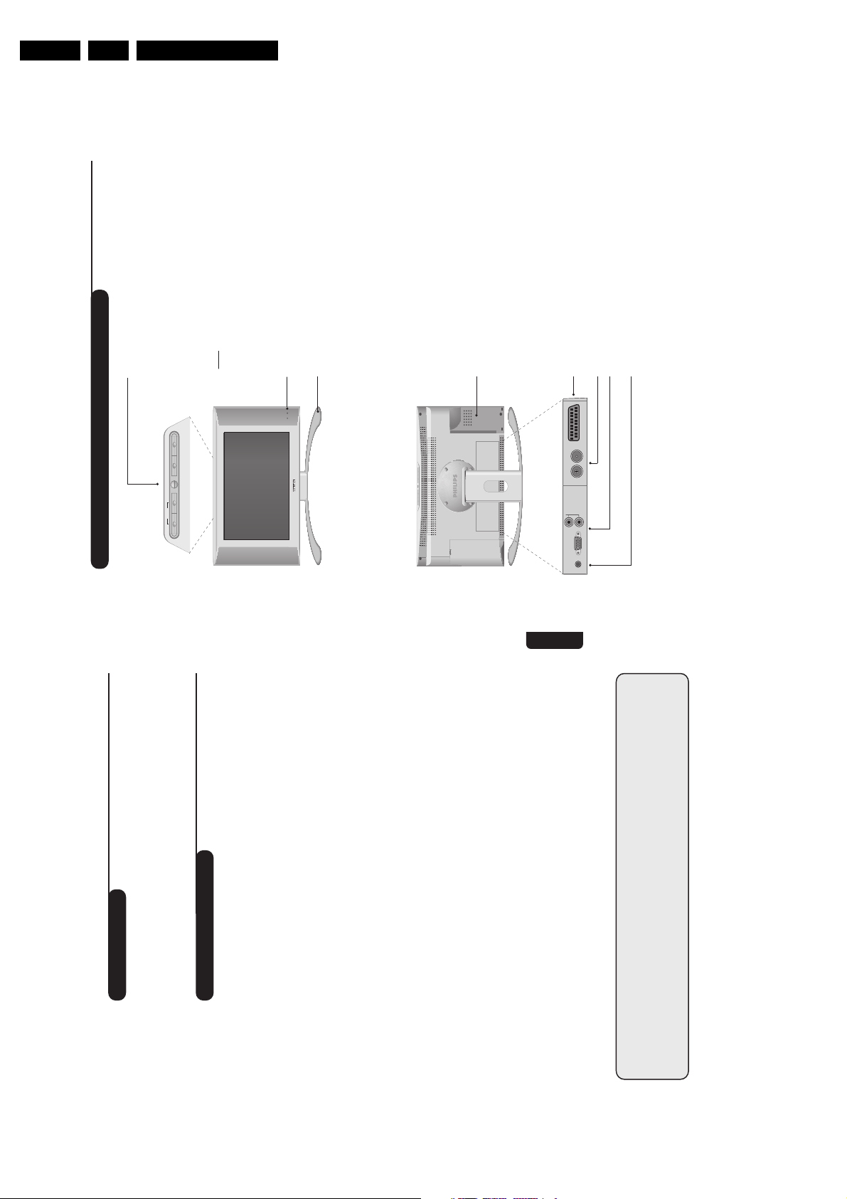
1.2.3 Rear Connections Part 2
S-Video
Video In
1.2.4 Rear Connections Part 3
L
R
DC In
PC Input (VGA)
Audio In (PC)
FM ANT
Figure 1-5 Rear Connections Part 3
DC - In
1 - 12 V_dc/5A/60W jr
VGA- in (Sub-D)
1
6
11
5
10
15
CL 16532023_043.eps
210901
Figure 1-6 VGA Connector
1 - Red 0.7 V_pp/75 ohm j
2 - Green 0.7 V_pp/75 ohm j
3 - Blue 0.7 V_pp/75 ohm j
4 - Sense Ground
5 - Ground
6 - Red Ground H
7 - Green Ground H
8 - Blue Ground H
9- +5V
10 - Sync Ground H
11 - Sense Ground H
12 - Bi-direct. data
13 - H-sync j
14 - V-sync j
15 - Data clock
EXT. 1
CL 36532054_020.eps
290703
L
Audio
R
CL 36532054_019.eps
290703
Figure 1-4 Rear Connections Part 2
S-VHS - In Hosiden
1 - Y Ground H
2 - C Ground H
3 - Y 1 V_pp/75 ohm j
4 - C 0.3 V_pp/75 ohm j
Video - In (Cinch)
1 - CVBS 1 V_pp/75 ohm jq
Audio - In (Cinch)
1 - Audio - L 0.5 V_rms/10 kohm jq
2 - Audio - R 0.5 V_rms/10 kohm jq
Audio - PC In
1 - Audio - R 0.5 V_rms/10 kohm jq
2 - Audio - L 0.5 V_rms/10 kohm jq
Aerial - In (IEC)
1 - IEC type 75 ohm, coax D
FM Ant (IEC)
1 - IEC type 75 ohm, coax D
SCART EXT1 - In/Out (RGB/YUV and CVBS)
121
CL96532137_056.eps
202
171199
Figure 1-7 SCART connector
1 - Audio - R 0.5 V_rms/1 kohm k
2 - Audio - R 0.5 V_rms/10 kohm j
3 - Audio - L 0.5 V_rms/1 kohm k
4 - Audio Ground H
5 - Blue Ground H
6 - Audio - L 0.5 V_rms/10 kohm j
Page 4
EN 4 LC03E1.
Technical Specifications, Connections, and Chassis Overview
7 -Blue 0.7 V_pp/75 ohm j
8 -CVBS-status 0 - 1.3 V: INT
4.5 - 7 V: EXT 16:9
9.5 - 12 V: EXT 4:3 j
9 -Green Ground H
10 - N.C.
11 - Green 0.7 V_pp/75 ohm j
12 - N.C.
13 - Red Ground H
14 - Blanking Ground H
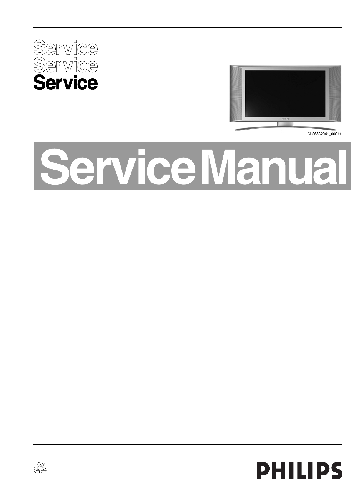
1.3 Chassis Overview
1.3.1 15”/17” model
TOP CONTROL PANEL
E
Right
Speaker
INVERTER PANEL
IN
LCD PANEL
TO LCD PANEL
15 - Red 0.7 V_pp/75 ohm j
16 - RGB-status/
FBL 0 - 0.4 V: INT
17 - Video in/out Ground H
18 - RGB sw. ctrl Ground H
19 - CVBS-out 1 V_pp/75 ohm k
20 - CVBS-in 1 V_pp/75 ohm j
21 - Common Ground H
1 - 3 V: EXT/75 ohm j
Left
Speaker
SIDE I/O PANEL
D
FRONT LED
J
PANEL
SCALER BOARD
C
1.3.2 23” model
TOP CONTROL PANEL
E
LCD PANEL
Figure 1-8 Chassis Overview 15”/17” model
To LCD
ComPair
TV BOARD
CL 36532023_067.eps
SIDE I/O PANEL
140403
A
D
SCALER BOARD
C
FRONT LED PANEL
J
Speaker assy R
To Inverter
ComPair
Figure 1-9 Chassis Overview 23” model
Speaker assy L
CL 36532044_022.eps
011003
TV BOARD
A
Page 5

Safety Instructions, Warnings, and Notes
2. Safety Instructions, Warnings, and Notes
EN 5LC03E 2.
2.1 Safety Instructions
Safety regulations require that during a repair:
• Always connect the set to the mains via an isolation
transformer (≥ 800 VA).
• Replace safety components, indicated by the symbol h,
only by components identical to the original ones.
Safety regulations require that after a repair, the set must be
returned in its original condition. Pay, in particular, attention to
the following points:
• Route the wire trees and HT cables correctly and fix them
with the mounted cable clamps.
• Check the insulation of the mains lead for external
damage.
• Check the cabinet for defects, to avoid touching of any
inner parts by the customer.
2.2 Warnings
• All ICs and many other semiconductors are susceptible to
electrostatic discharges (ESD w). Careless handling
during repair can reduce life drastically. Make sure that,
during repair, you are connected with the same potential as
the mass of the set by a wristband with resistance. Keep
components and tools also at this same potential.
Available ESD protection equipment:
– Complete kit ESD3 (small tablemat, wristband,
connection box, extension cable and earth cable) 4822
310 10671.
– Wristband tester 4822 344 13999.
• Be careful during measurements in the high voltage
section (on the inverter panel).
• Never replace modules or other components while the unit
is switched 'on'.
• When you align the set, use plastic rather than metal tools.
This will prevent any short circuits and the danger of a
circuit becoming unstable.
2.3 Notes
2.3.1 General
• Clean the LCD display with a slightly humid cloth.
• Measure the direct voltages and oscillograms with regard
to the chassis ground (H), or hot ground (I) as this is
called.
• The direct voltages and oscillograms shown in the
diagrams are indicative. Measure them in the Service
Default Mode (see section “Service Modes”).
• Where necessary, measure the voltages in the power
supply section both in normal operation (G) and in standby
(F). These values are indicated by means of the
appropriate symbols.
• The semiconductors indicated in the circuit diagram and in
the parts lists, are interchangeable per position with the
semiconductors in the unit, irrespective of the type
indication on these semiconductors.
• Capacitor values may also use the value multiplier as the
decimal point indication (e.g. 2p2 indicates 2.2 pF).
• An 'asterisk' (*) indicates component usage varies. Refer to
the diversity tables for the correct values.
• The correct component values are listed in the Electrical
Replacement Parts List. Therefore, always check this list
when there is any doubt.
2.3.3 Rework on BGA ICs
General
Although (LF)BGA assembly yields are very high, there may
still be a requirement for component rework. By rework, we
mean the process of removing the component from the PWB
and replacing it with a new component. If an (LF)BGA is
removed from a PWB, the solder balls of the component are
deformed drastically so the removed (LF) BGA has to be
discarded.
Device Removal
As is the case with any component, it is essential when
removing an (LF) BGA that the board, tracks, solder lands, or
surrounding components are not damaged. To remove an
(LF)BGA, the board must be uniformly heated to a temperature
close to the reflow soldering temperature. A uniform
temperature reduces the chance of warping the PWB.
To do this, we recommend that the board is heated until it is
certain that all the joints are molten. Then carefully pull the
component off the board with a vacuum nozzle. For the
appropriate temperature profiles, see the IC data sheet.
Area Preparation
When the component has been removed, the vacant IC area
must be cleaned before replacing the (LF)BGA.
Removing an IC often leaves varying amounts of solder on the
mounting lands. This excessive solder can be removed with
either a solder sucker or solder wick. The remaining flux can be
removed with a brush and cleaning agent.
After the board is properly cleaned and inspected, apply flux on
the solder lands and on the connection balls of the (LF) BGA.
Note: Do not apply solder paste, as this has shown to result in
problems during re-soldering.
Device Replacement
The last step in the repair process is to solder the new
component on the board. Ideally, the (LF)BGA should be
aligned under a microscope or magnifying glass. If this is not
possible, try to align the (LF)BGA with any board markers.
To reflow the solder, apply a temperature profile according to
the IC data sheet. So as not to damage neighbouring
components, it may be necessary to reduce some
temperatures and times
2.3.2 Schematic Notes
• All resistor values are in ohms and the value multiplier is
often used to indicate the decimal point location (e.g. 2K2
indicates 2.2 kohm).
• Resistor values with no multiplier may be indicated with
either an 'E' or an 'R' (e.g. 220E or 220R indicates 220
ohm).
• All Capacitor values are expressed in Micro-Farads (µ=
-6
x10
), Nano-Farads (n= x10-9), or Pico-Farads (p= x10
-12
).
Page 6
EN 6 LC03E3.
2
.
”
P
PROGRAM
VOLUME
MENU
+
-
+
-
Presentation of the LCD Television
L
R
Audio in (PC)
DC in PC input (VGA)
FM ANT
EXT. 1
:
Ø
Television keys:
• .: to switch the TV on or off.
• VOLUME - + (-”+): to adjust sound level.
• PROGRAM - + (- P +):to select programmes.
• MENU: to access or close menus, simultaneously
press the ” - and ” + keys. The - + keys can be
used to select an adjustment and the ” - + keys to
make that adjustment.
Note
: when the CHILD LOCK function is activated the
-”+ and - P + keys are unavailable (refer to FEATURES
menu on page 10).
On-light and infrared sensors.
Adjustable stand.
The stand can be removed and replaced with a wall
mounting kit available as an option (ask your dealer).
Rear of set :
The main connections are made at the bottom of the
television.
Removable panels to left* and right access the
supplementary connection sockets.
* The large screen sizes do not have a left panel. For more
details on connections see page 14.
EXT1 socket
TV and radio aerial sockets
VGA and audio input for connecting a computer.
DC supply socket
1
Introduction
Table of Contents
Thank you for purchasing this television set.
This handbook has been designed to help you install and operate your TV set.
We would strongly recommend that you read it thoroughly.
We hope our technology meets entirely with your satisfaction.
Installation
Presentation of the LCD Television . . . . . . . . . . . . . . . . . . . . . . . . . . . . . . . . . . . . .4
The remote control keys . . . . . . . . . . . . . . . . . . . . . . . . . . . . . . . . . . . . . . . . . . . .3
Installing your television set . . . . . . . . . . . . . . . . . . . . . . . . . . . . . . . . . . . . . . . . . .4
Quick installation . . . . . . . . . . . . . . . . . . . . . . . . . . . . . . . . . . . . . . . . . . . . . . . . . .5
Sorting programmes . . . . . . . . . . . . . . . . . . . . . . . . . . . . . . . . . . . . . . . . . . . . . . . .5
Choosing a language and country . . . . . . . . . . . . . . . . . . . . . . . . . . . . . . . . . . . . .6
Automatic tuning . . . . . . . . . . . . . . . . . . . . . . . . . . . . . . . . . . . . . . . . . . . . . . . . . .6
EasyLink function . . . . . . . . . . . . . . . . . . . . . . . . . . . . . . . . . . . . . . . . . . . . . . . . . . .6
Manual tuning . . . . . . . . . . . . . . . . . . . . . . . . . . . . . . . . . . . . . . . . . . . . . . . . . . . . .7
Programme name . . . . . . . . . . . . . . . . . . . . . . . . . . . . . . . . . . . . . . . . . . . . . . . . . .7
Operation
Using the radio . . . . . . . . . . . . . . . . . . . . . . . . . . . . . . . . . . . . . . . . . . . . . . . . . . . . .8
Using in PC monitor mode . . . . . . . . . . . . . . . . . . . . . . . . . . . . . . . . . . . . . . . . . . .8
Adjusting the picture . . . . . . . . . . . . . . . . . . . . . . . . . . . . . . . . . . . . . . . . . . . . . . .9
Adjusting the sound . . . . . . . . . . . . . . . . . . . . . . . . . . . . . . . . . . . . . . . . . . . . . . . .9
Feature settings . . . . . . . . . . . . . . . . . . . . . . . . . . . . . . . . . . . . . . . . . . . . . . . . . . . .9
Timer function . . . . . . . . . . . . . . . . . . . . . . . . . . . . . . . . . . . . . . . . . . . . . . . . . . .10
Locking the set . . . . . . . . . . . . . . . . . . . . . . . . . . . . . . . . . . . . . . . . . . . . . . . . . . .10
Teletext . . . . . . . . . . . . . . . . . . . . . . . . . . . . . . . . . . . . . . . . . . . . . . . . . . . . . . . . .11
16:9 Formats . . . . . . . . . . . . . . . . . . . . . . . . . . . . . . . . . . . . . . . . . . . . . . . . . . . . .12
Video recorder or DVD keys . . . . . . . . . . . . . . . . . . . . . . . . . . . . . . . . . . . . . . . .13
Glossary . . . . . . . . . . . . . . . . . . . . . . . . . . . . . . . . . . . . . . . . . . . . . . . . . . . . . . . .13
Peripherals
Video recorder . . . . . . . . . . . . . . . . . . . . . . . . . . . . . . . . . . . . . . . . . . . . . . . . . . .14
Other equipment . . . . . . . . . . . . . . . . . . . . . . . . . . . . . . . . . . . . . . . . . . . . . . . . .14
To select connected equipment . . . . . . . . . . . . . . . . . . . . . . . . . . . . . . . . . . . . .14
Video camera, video games . . . . . . . . . . . . . . . . . . . . . . . . . . . . . . . . . . . . . . . . . .15
Headphones . . . . . . . . . . . . . . . . . . . . . . . . . . . . . . . . . . . . . . . . . . . . . . . . . . . . . 15
Amplifier . . . . . . . . . . . . . . . . . . . . . . . . . . . . . . . . . . . . . . . . . . . . . . . . . . . . . . . . .15
Computer . . . . . . . . . . . . . . . . . . . . . . . . . . . . . . . . . . . . . . . . . . . . . . . . . . . . . . .15
Tips . . . . . . . . . . . . . . . . . . . . . . . . . . . . . . . . . . . . . . . . . . . . . . . . . . . . . . . . . . .16
°
Recycling
The materials used in your set are either reusable or can be recycled.
To minimise environmental waste, specialist companies collect used appliances
and dismantle them after retrieving any materials that can be used again (ask
your dealer for further details).
English
3. Directions for Use
Directions for Use
Page 7

Directions for Use
4
& Positioning the television set
Place your TV on a solid stable surface. To avoid
danger do not expose the TV to water,or a heat
source (e.g. lamp, candle,radiator). Do not obstruct
the ventilation grid at the rear.
é
Connecting the aerials
• Use the aerial connection lead supplied and
connect the
:
socket situated at the bottom of
the TV to your aerial socket.
• Insert the radio aerial lead supplied into the FM
ANT socket located at the bottom of the TV.
• Arrange the leads by passing them through the
television stand.
“
Power supply connections
The TV works with a DC supply (the voltage is
indicated on the label). Only use the AC-DC
adaptor supplied with the TV.
• Connect the DC plug of the adaptor to the TV DC
socket. Leave a space round the adaptor for
ventilation.
• Insert the adaptor power lead and insert the mains
plug into the wall socket.
For connecting other appliances see page p.14.
‘
Remote control
Insert the two R6-type batteries supplied, making
sure they are the right way round.
The batteries supplied with the appliance do not
contain mercury or nickel cadmium so as to protect
the environment. Please do not discard your used
batteries, but use the recycling methods available
(consult your distributor).
(
Switching on
To switch on the set, press the on/off key. A green
indicator comes on and the screen lights up. Go
straight to the Quick Installation chapter on page 5.
If the TV remains in standby mode(red indicator),
press the P
#
key on the remote control.
The indicator will flash when you use the remote control.
Installing your television set
5 cm
5 cm
5 cm
FM ANT.
.
”
P
PROGRAM
VOLUME
MENU
++
--
3
12
MODE
MUTE
RADIO
VCR
DVD
SMARTSMART ACTIVE
CONTROL
MENU
PC TV
OK
P
564
879
0
·¢Ê
∆
Æ
∫
ù
¤Ó
`
Ÿı
Å
Ë
Á
∏
3
--
++
.
ª
-
[
”
Y
ª
Remote control keys
Select peripherals (p.14)
Press several times to select the
required EXT connector.
Teletext keys (p.11)
or VCR / DVD (p.13)
œ
PIP on/off (p. 8)πMove PIP (p.8)
Sleeptimer
To select the length of time before
the set automatically switches to
standby (from 0 to 240 minutes)
Active control
Optimizes the quality of the picture
according to the quality of reception.
Sound mode
Used to force programmes in STEREO
and
NICAM STEREO
to
MONO
or,
for bilingual programmes, to choose
between
DUAL I
or
DUAL II
.
When the sound mode is switched to
MONO, the indication is displayed in red.
Menu
To call up or exit the menus.
Cursor
These 4 keys are used to move
around the menus.
Volume
To adjust the sound level
PC / TV / Radio
Press one of these keys to switch
the television between PC,TV or
radio mode (p. 8).
16:9 formats (p.12)
Mute
To mute or restore the sound.
Screen information
To display / remove the programme
number,the name (if it exists), the
time, the sound mode and the time
remaining on the timer. Hold down
for 5 seconds to permanently
display the programme number on
the screen.The volume level and the
smart control adjustments are then
displayed each time they are used.
Standby
To set the TV to standby mode.To
switch the TV set on again, press
b
,P
@#
or
09
.
List of programmes
To display/ clear the list of programmes.
Use the keys
îÏ
to select a
programme and the key
¬
to display it.
The symbol
+
is displayed alongside
all programmes which are locked (p.10)
or
?
if they are not locked.
Smart picture and sound
Used to access a series of predefined
picture and sound settings.
The PERSONAL position relates to
settings selected from the menus.
Surround sound
To activate
/
deactivate the surround
sound effect. In stereo, this gives the
impression that the speakers are further
apart. For models equipped with Virtual
Dolby Surround*,you can obtain Dolby
Surround Pro Logic sound quality. In
mono,a stereo spatial effect is simulated.
* Manufactured under license from Dolby
Laboratories Licensing Corporation. ”Dolby””Pro Logic”
and the double-D symbol
£
are trademarks of
Dolby Laboratories Licensing Corporation.
Selecting TV programmes
To move up or down a programme.
The number,(the name) and the sound
mode are displayed for a few seconds.
For some TV programmes the title of
the programme appears at the bottom
of the screen.
Previous programme
To access the previously viewed
programme.
Numerical keys
For direct access to programmes.
For a 2 digit programme number,
the 2
nd
digit must be entered
before the dash disappears.
Mode selector (p. 13)
To activate the remote control in
TV,VCR (video recorder) or DVD
mode.
EN 7LC03E 3.
Page 8
EN 8 LC03E3.
6
Choosing a language and country
Automatic tuning
& Press the
H
key to display the main menu.
é Select INSTALL (
Ï
), then press
¬
.
The INSTALL menu appears.
The LANGUAGE option is activated.
“ Press
¬
to go into the LANGUAGE menu.
‘ Select your language with the
îÏ
keys.
The menus will appear in the chosen language.
( Press
È
to exit the LANGUAGE menu.
§ Select the option COUNTRY and press
¬
.
è Select your country with
îÏ
keys.
If your country does not appear in the list, select
OTHER.
! Press
È
to exit the COUNTRY menu.
ç To exit from the menus,press
d
.
See also: EasyLink function below.
This menu allows you to automatically search
for all the programmes available in your region
(or on your cable network).
& First carry out operations & to ! above, then:
é Press
Ï
once to select AUTO STORE then
press
¬
.The search begins.
After several minutes,the INSTALL menu
reappears automatically.
“ If the transmitter or the cable network
broadcasts the automatic sort signal, the
programmes will be correctly numbered.
‘ If not, the programmes found will be
numbered in descending order starting at 99,
98, 97,etc.
Use the SORT menu to renumber them.
Some transmitters or cable networks broadcast
their own sort parameters (region, language,etc.).
Where this is the case, make your choice using the
îÏ
keys and confirm with
¬
.
To exit or interrupt the search, press the
H
key. If
no picture is found, refer to the chapter entitled
Tips on p. 16.
See also: EasyLink function below.
( To exit from the menus, press
d
.
• PICTURE
• SOUND
• FEATURES
• INSTALL
INSTALL
• LANGUAGE
• COUNTRY
• AUTO STORE
• MANUAL STORE
• SORT
•
NAME
ENGLISH
DANSK
NEDERLANDS
INSTALL
• LANGUAGE
• COUNTRY
• AUTO STORE
• MANUAL STORE
• SORT
•
NAME
SEARCHING
PLEASE WAIT
PROG. NO. 2
215.18 MHZ
If the set is connected (by the EXT2 socket)
to a video equipped with the EasyLink
function, the language,country and channels
found are automatically transmitted to the
video recorder at the time of installation.
A message is displayed on-screen during
loading.The list of video recorder channels is
then the same as those of the set.
The EASY LINK setting in the OPTIONS menu
must be set to ON (default setting), see page 9.
EasyLink function
(only available on certain versions)
5
Quick installation
Sorting programmes
The first time you switch on the television,a
menu appears on the screen.This menu asks
you to choose the language of the menus :
If the menu does not appear, hold down the
”
- and
”
+ keys on the set for 5 seconds to bring it up.
& Use the
îÏ
keys on the remote control to
choose your language then confirm with
¬
.
é Then select your country using the
îÏ
keys and confirm with
¬
.
If your country does not appear in the list, select “.. .”
“ Tuning starts automatically.
The operation takes several minutes.
A display shows the search status and the
number of programmes found.When it has
finished the menu disappears.
To exit or interrupt the search, press the
H
key.
If no programmes are found, refer to the chapter
entitled Tips on p. 16.
‘ If the transmitter or the cable network
broadcasts the automatic sort signal, the
programmes will be correctly numbered.
( If not, the programmes found will be numbered
in descending order starting at 99, 98,97, etc.
Use the SORT menu to renumber them.
Some transmitters or cable networks broadcast
their own sort parameters (region, language,etc.).
Where this is the case, make your choice using the
îÏ
keys and confirm with
¬
.
See also: EasyLink function,page 6.
& Press the
H
key.The main menu is displayed.
é Select INSTALL (
Ï
), then press
¬
.
The INSTALL menu appears.
“ Using the
Ï
key, select SORT then press
¬
.The SORT menu appears.The FROM
option is activated.
Note:
this menu works as follows:
• Change "FROM" (enter the current programme
number),
• "TO" (enter the new number),
• EXCHANGE numbers" (the operation is carried out).
‘ Select the programme you wish to renumber
using
Ȭ
keys or
0
to
9
.
Example: to renumber programme 78 as 2
press
78
.
( Select TO (using
Ï
key) and enter the new
number with
Ȭ
keys or
0
to
9
(for
the example given, enter
2
).
§ Select EXCHANGE (
Ï
key) and press
¬
.
The message EXCHANGED appears, the
exchange takes place. In our example,
programme 78 is renumbered as 2 (and
programme 2 as 78).
è Select the option FROM (
î
key) and repeat
stages ‘ to § as many times as there are
programmes to renumber.
See also: EasyLink function,page 6.
! To exit from the menus, press
d
.
• PICTURE
• SOUND
• FEATURES
• INSTALL
INSTALL
• LANGUAGE
• COUNTRY
• AUTO STORE
• MANUAL STORE
• SORT
• NAME
FROMTOEXCHANGE
SELECT LANGUAGE
LANGUAGE
•
ENGLISH
DANSK
NEDERLANDS
FINNISH
FRANCAIS
COUNTRY
AUSTRIA
BELGIUM
SWITZERLAND
GERMANY
DENMARK
Directions for Use
Page 9
Directions for Use
8
Using the radio
Using in PC monitor mode
Choosing radio mode
Press the
Z
key on the remote control to
switch the TV to radio mode. Press the
X
key to return to TV mode. In radio mode the
number and name of the station (if available),
its frequency and the sound mode are
indicated on the screen.
To enter the name of the stations use the NAME
menu. (p.7)
Selecting programmes
Use the
09
or
@
P
#
keys to select the
FM stations (from 1 to 40).
List of radio stations
Press the
ı
key to display / hide the list of
radio stations. Then use the cursor to select a
station.
Using the radio menus
Use the
H
key to access the specific radio
settings.
Searching radio stations
If you have used the quick installation all the
available FM stations will be stored. To start a
new search use the INSTALL menu :AUTO
STORE (for a complete search) or MANUAL
STORE (for a station by station search). The
SORT and NAME menus let you classify or
name the radio stations. These menus work in
exactly the same way as the TV menus.
Screen saver
In the FEATURES menu you can activate / close
the screen saver. The time, the frequency of
the station and its name (if available) move
across the screen.
PC Mode
Your TV can be used as a computer monitor.
The PIP function lets you display a
superimposed image to watch the TV channels
at the same time.
You must first of all connect the computer and
adjust the resolution (see p.15).
Choosing PC mode
Press the
V
key on the remote control to
switch the TV to PC mode. Press the
X
key
to return to TV mode.
If there is no PC signal for more than five seconds,
the TV automatically goes into standby mode.
Using PIP
While in PC mode you can call up a window
for TV channels.
& Press the
œ
key to display the PIP screen.
The television image is reproduced in a small
superimposed window.
é Press the
œ
key again to reduce the size of
the window then make it disappear.
“ Use the
π
key if you want to hide the
window. You can also shift it progressively by
using the cursor.
‘ Use the
09
or
@
P
#
keys to change the
programmes of the PIP screen or the
n
key
if you want to display a picture from an
appliance connected to the TV (e.g. video
recorder, DVD).
Using the PC menus
Press the
H
key to access the specific settings of
the PC monitor mode. Use the cursor to adjust
them (the settings are automatically saved) :
•
AUDIO SELECTION
:
to choose the sound
reproduced on the TV (PC or TV/Radio).
For example, you can listen to the radio while
you use the computer.
Note: you must choose TV or radio mode before
going into PC mode. You cannot listen to the radio
when the PIP screen is displayed.
•
BRIGHTNESS / CONTRAST
: to adjust the
brightness and contrast.
•
ADJUST COLOUR
:
to adjust the colours (cold,
normal or warm).
•
VIDEO NOISE
:
eliminates the horizontal (PHASE)
and vertical (CLOCK) interfering lines.
•
ADJUST POSITION
:
to adjust the horizontal and
vertical placing of the image.
•
AUTOADJUST
:
position is set automatically.
•
PIP CONTROLS
:
to adjust the size and position
of the PIP screen.
•
MODE SELECT
:
to come back to TV or radio
mode.
•
RESET TO FACTORY SETTING
:
to return to the
factory settings (default settings).
•
VIEW FORMAT
:
to choose between large screen
or the original format of the PC screens.
7
Manual tuning
Programme name
This menu allows you to store the
programmes one by one.
& Press
H
.
é Select INSTALL (
Ï
), then press
¬
.
The INSTALL menu appears.
“ Select MANUAL STORE (
Ï
) then press
¬
.
The menu appears :
‘ Press
¬
to go to the SYSTEM menu.
Use
îÏ
to choose EUROPE (automatic
detection*) or manual detection with WEST
EUR (standard BG reception), EAST EUR
(standard DK reception), UK (standard I
reception) or FRANCE (standard LL').
Then press
È
to exit from the menu.
* Except for France (standard LL'): select the
option FRANCE.
( Select SEARCH and press
¬
.
The search begins.As soon as a programme is
found, the search will stop. If you know the
frequency of the programme required,enter
its number directly using the
09
keys and
go to step è.
If no programme is found, refer to the Tips chapter
on page 16).
§ If reception is un-satisfactory, select FINE
TUNE and hold down
È
or
¬
key.
è Select PROG.NO (programme number) and
use the
Ȭ
or
0
to
9
keys to enter
the desired number.
! Select STORE and press
¬
.The message
STORED appears.The programme is stored.
See also: EasyLink function,page 6.
ç Repeat steps ( to ! for each programme to
be stored.
To exit: press the
d
key.
You may,if you wish, give a name to the first
40 programmes (from 1 to 40).
& Press
H
.
é Select INSTALL (
Ï
), then press
¬
.
The INSTALL menu appears.
“ Press
Ï
5 times to select NAME (concealed
at the bottom of the screen), then press
¬
.
The menu appears :
‘ Select the programme you wish to name using
the keys
09
or
@
P
#
.
Note:
at the time of installation, the programmes
are automatically named when the identification
signal is transmitted.
( Use the keys
Ȭ
to move within the
name display area (5 characters).
§ Use keys
îÏ
to choose the characters.
è Press
H
when the name has been entered.
The programme name is stored.
See also: EasyLink function,page 6.
! Repeat steps ‘ to è for each programme to
be named.
ç To exit from the menus,press
d
.
• PICTURE
• SOUND
• FEATURES
• INSTALL
INSTALL
MANUAL STORE
• SYSTEM
• SEARCH
• PROG. NO.
• FINE TUNE
• STORE
EUROPE
WEST EUR
EAST EURUKFRANCE
INSTALL
• LANGUAGE
• COUNTRY
• AUTO STORE
• MANUAL STORE
• SORT
•
NAME
BBC_1
EN 9LC03E 3.
Page 10
EN 10 LC03E3.
10
Timer function
Locking the set
This menu allows you to use your TV as an
alarm clock.
& Press
H
.
é Select
FEATURES
(
Ï
) and press
¬
twice.
The
TIMER
menu appears :
“ Press
¬
to enter and exit the sub-menus
and use keys
îÏ
to adjust:
‘
TIME
: enter current time.
Note:
the time is updated automatically each time
the set is switched on using teletext information
taken from programme 1. If programme 1 does
not have teletext, the update will not take place.
(
START TIME
: enter the start time.
§
STOP TIME
: enter the stop time.
è
PROG.NO.
: enter the number of the
programme required.
!
ACTIVATE
: you can set the alarm to be
activated:
•
ONCE ONLY
for a one-off alarm,
•
DAILY
for a daily alarm or
•
STOP
to cancel.
ç Press
b
to set the TV to standby.It will
automatically switch on at the time
programmed. If you leave the TV switched on,
it will only change programme at the time
indicated.
The combination of the CHILD LOCK and TIMER
functions may be used to limit the length of time
your television is in use, for example, by your
children.
You can bar access to certain programmes or
completely lock the set by locking the keys.
Locking programmes
& Press
H
.
é Select (
Ï
) and press
¬
.
“ Select
PARENTAL. CONT.
(
Ï
) and press
¬
.
‘ Enter your confidential access code.The first
time, enter the code 0711 then confirm by
re-entering 0711.The menu appears.
( Press
¬
to go into the menu.
§ Use keys
îÏ
to select the required
programme and confirm with
¬
.The symbol
+
is displayed alongside the programmes or
sockets that have been locked.
è Press
d
to exit.
To watch a programme which has been locked
you will now need to enter the confidential
code; otherwise the screen will remain blank.
The INSTALL menu access is also locked.
Caution:
in the case of encrypted programmes
which use an external decoder, it is necessar y to
lock the corresponding EXT socket.
To unlock all programmes
Repeat stages & to ‘ above, then select
CLEAR ALL
and press
¬
.
To change the confidential code
Repeat stages & to ‘ above, then:
( Select
CHANGE CODE
and enter your own 4-
digit number.
§ Confirm by entering it again.
Your new code will be stored.
è Press
d
to exit from the menus.
If you have forgotten your confidential code, enter
the universal code 0711 twice.
Locking the keys
& Press
H
, select
FEATURES
(
Ï
) and press
¬
.
é Select
CHILD LOCK
(
Ï
) and press
¬
to set
the lock to
ON
.
“ Switch off the set and put the remote control
out of sight.The set cannot be used (it can only
be switched on using the remote control).
‘ To cancel: switch
CHILD LOCK
to
OFF
.
• PICTURE
• SOUND
• FEATURES
• INSTALL
FEATURES
TIMER
• TIME
• START TIME
• STOP TIME
• PROG; NO;
• ACTIVATE
10:56
• PICTURE
• SOUND
• FEATURES
• INSTALL
FEATURES
• TIMER
• CHILD LOCK
• PARENTAL CONT
• ROTATION
ACCES CODE
- - - -
9
Adjusting the picture
Adjusting the sound
& Press
H
then
¬
.
The
PICTURE
menu appears :
é Use
îÏ
keys to select a setting and
Ȭ
keys to adjust.
Note:
the menu is a scroll-down menu.
Keep the key
Ï
held down to access the
settings hidden at the bottom of the screen.
“ Once the necessary adjustments have been
made, select the option
STORE
and press
¬
to store them.
‘ To exit from the menus, press
d
.
Description of the settings:
•
BRIGHTNESS
: alters the brightness of the
image.
•
COLOUR
: alters the colour intensity.
•
CONTRAST
: alters the variation between
light and dark tones.
•
SHARPNESS: alters the crispness of the image.•STORE
: stores the picture settings.
•
COLOUR TEMP.
: adjusts the colour
temperature of the picture.Three options
are available here:
COOL
(blue white),
NORMAL
(balanced) or
WARM
(red white).
•
CONTRAST +
:To activate / de-activate the
automatic contrast adjustment system (the
dark areas are made darker whilst
maintaining the detail).
& Press
H
, select the
SOUND
option (
Ï
) and
press
¬
.The
SOUND
menu appears :
é Use
îÏ
keys to select a setting and keys
Ȭ
to adjust.
“ Once the necessary adjustments have been
made, select the option
STORE
and press
¬
to store them.
‘ To exit from the menus, press
d
.
Description of the settings:
•
EQUALIZER
: to adjust the sound tone (from
bass: 120 Hz to treble: 10 kHz).
•
BALANCE
: to balance the sound between the
left and right speakers.
•
DELTA VOLUME
(volume difference):allows
you to compensate for the volume differences
between the different programmes or the
EXT sockets.This setting is available for
programmes 1 - 40 and the EXT sockets.Use
the
@
P
#
keys to compare the level of
different programmes.
•
STORE
: stores the sound settings.
•
AVL
: automatic volume control used to avoid
sudden increases in volume,particularly when
changing programmes or during advertisements
• PICTURE
• SOUND
• FEATURES
• INSTALL
PICTURE
• BRIGHTNESS
• COLOUR
• CONTRAST
• SHARPNESS
• STORE
• COLOUR TEMP.
• CONTRAST+
--I------ 39
• PICTURE
• SOUND
• FEATURES
• INSTALL
SOUND
• EQUALIZER
•
SURROUND MODE
• DELTA VOLUME
• STORE
• AVL
120 HZ
500 HZ
1500 HZ
5 KHZ
10 KHZ
Feature settings
& Press
H
, select
FEATURES
(
Ï
) and press
¬
.You can adjust:
é
TIMER
,
PARENTAL. CONT.
and
CHILD LOCK
:
see next page
“
MODE SELECT.
: to switch the TV in radio,TV or
PC mode.
‘
EASYLINK
(only available on certain versions) : If
the set is connected (by the EXT2 socket) to
a video equipped with the EasyLink function,
the language, country and channels found are
automatically transmitted to the video
recorder at the time of installation. If your
video recorder is not equipped with this
function, set to
OFF
.
( To quit the menus, press
d
.
Directions for Use
Page 11
Directions for Use
12
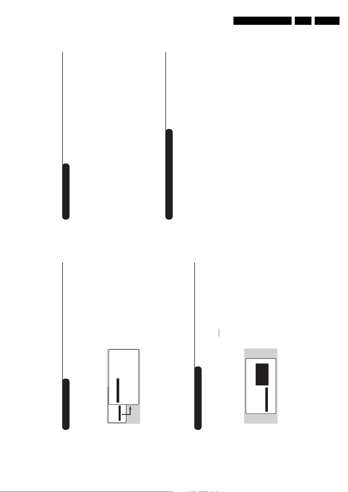
16:9 Formats
The pictures you receive may be transmitted in 16:9 format (wide screen) or 4:3 format
(conventional screen).4:3 pictures sometimes have a black band at the top and bottom of the screen
(letterbox format).This function allows you to optimise the picture display on screen.
If your television is equipped with a 4:3 screen.
If your television is equipped with a 16:9 screen.
Press the
p
key (or
Ȭ
) to select the different modes:
This TV set is also equipped with automatic switching which will select the correct-screen
format, provided the specific signals are transmitted with the programmes.
4:3
The picture is reproduced in 4:3 format and a black band is displayed on either side
of the picture.
ZOOM 14:9
The picture is enlarged to 14:9 format, a thin black band remains on both sides of
the picture.
ZOOM 16:9
The picture is enlarged to 16:9 format.This mode is recommended when displaying
pictures which have black bands at the top and bottom (letterbox format).
SUBTITLE ZOOM
This mode is used to display 4:3 pictures using the full surface of the screen leaving
the sub-titles visible.
SUPER WIDE
This mode is used to display 4:3 pictures using the full surface of the screen by
enlarging the sides of the picture.
WIDE SCREEN
This mode restores the correct proportions of images transmitted in 16:9.
Note:
If you display a 4:3 picture in thid mode, it will be enlarged horizontally.
FULL SCREEN
This mode displays images in full screen.
Press the
p
key (or
îÏ
) to select the different modes:
4:3
The picture is reproduced in 4:3 format.
EXPAND 4:3
The picture is enlarged vertically.This mode is used to cancell the black bands when
watching a programme in letterbox format.
COMPRESS 16:9
The picture is compressed vertically into 16:9 format.
11
Å
P
9
0
MENU
Y
Ë
Ë
ù
12
MODE
MUTE
VCR
DVD
SMART SMART
RADIO
ACTIVE
CONTROL
MENU
OK
PC TV
P
564
879
0
`
¤
Ó
ù
Ÿ
Å
%
∆
ı
∫
Ë
Á
∏
3
- -
+ +
.
ª
-
[
”
Y
ª
Teletext
Press :
You will obtain:
Teletext is an information system broadcast by certain channels which can be consulted like a
newspaper. It also offers access to subtitles for viewers with hearing problems or who are not familiar
with the transmission language (cable networks, satellite channels, etc.).
Teletext
call
Selecting
a page
This is used to call teletext, change to transparent mode and
then exit.The summary appears with a list of items that can be
accessed. Each item has a corresponding 3 digit page number.
If the channel selected does not broadcast teletext, the indication
100 will be displayed and the screen will remain blank (in this
case, exit teletext and select another channel).
Enter the number of the page required using the
0
to
9
or
@ P #
keys.Example: page 120,enter
120
.The
number is displayed top left,the counter turns and then the
page is displayed.Repeat this operation to view another
page.
If the counter continues to search, this means that the page is
not transmitted. Select another number.
Contents
Direct
access to
the items
This returns you to the contents page (usually page 100).
Coloured areas are displayed at the bottom of the screen.
The 4 coloured keys are used to access the items or
corresponding pages.
The coloured areas flash when the item or the page is not yet
available.
Direct
selection of
sub-pages
Certain pages contain sub-pages (for example, page 120
contains sub-pages
1/3, 2/3 and 3/3).If this is the case, the
page number is displayed in green,preceded by the symbol
Æ
,
Í
or
ÍÆ
. Use the keys
Ȭ
to directly access
the sub-pages of your choice.
Enlarge
a page
Double page
teletext
This allows you to display the top or bottom part of the
page and then return to normal size.
To activate or deactivate the double page teletext display
mode.The active page is displayed on the left and the
following page is displayed on the right.Press
s
if you want
to hold a page (i.e. the contents page).The active page is then
displayed on the right.To return to normal mode, press
e
.
Hidden
information
Favourite
pages
To display or hide the concealed information (games solutions).
Instead of the standard coloured areas displayed at the bottom
of the screen, you can store 4 favourite pages on the first 40
channels which can then be accessed using the coloured keys
(red, green, yellow, blue).Once set, these favourite pages will
become the default every time tetetext is selected.
&
Press the
H
key to change to favourite pages mode.
é
Display the teletext page that you want to store.“Press
d
then the coloured key of your choice.The
page is stored.
‘
Repeat steps
é
and
“
for the other coloured keys.
(
Now when you consult teletext, your favourite pages
will appear in colour at the bottom of the screen.
To temporaly retrieve the standard items,press
H
.
To clear everything, and return the standard items as the
default, press
d
for 5 seconds.
EN 11LC03E 3.
Page 12
EN 12 LC03E3.
14
MODE
VCR
DVD
·¢Ê Æ
∫
Ó
ı
Ω∆
.
Z
¤
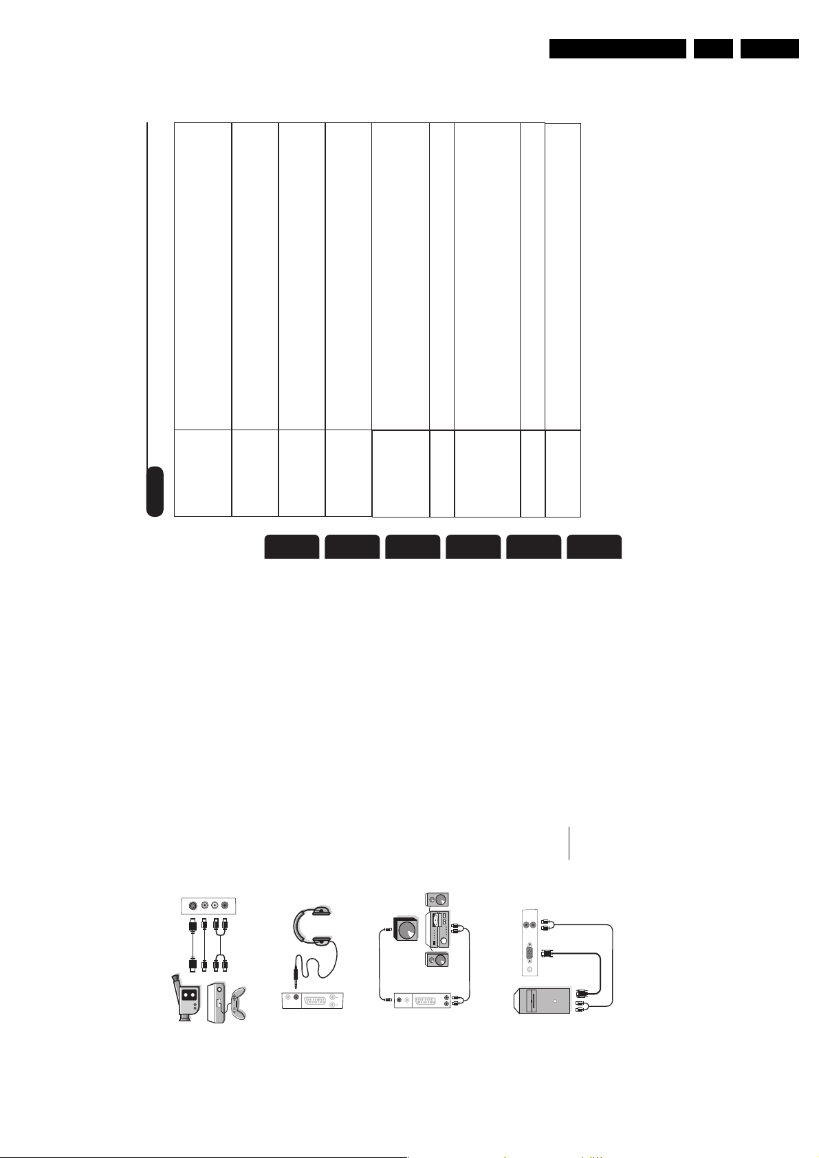
Connecting peripheral equipment
Depending on the version the TV is equipped with one or two EXT1 and EXT2 sockets.
A special adaptor is supplied to connect to EXT1 and can route the leads to the back.
The EXT1 socket has audio, CVBS/RGB inputs and audio, CVBS outputs.
The EXT2 socket (if available) has audio, CVBS/S-VHS inputs and audio, CVBS outputs.
Video recorder (or DVD recorder)
Carry out the connections shown opposite, using a good
quality euroconnector cable. If your video recorder has the
Easylink function, use the EXT2 socket.
If your video recorder does not have a euroconnector socket, the
only connection possible is via the aerial cable.You will therefore
need to tune in your video recorder's test signal and assign it
programme number 0 (refer to manual store, p. 6).
To reproduce the video recorder picture,press
0
.
Video recorder with decoder
Connect the decoder to the second euroconnector socket of
the video recorder.You will then be able to record scrambled
transmissions.
Video recorder
Satellite receiver, decoder, DVD,games, etc.
For TV sets with 2 SCART connectors,preferably connect the
equipment delivering RGB signals (digital decoders, DVD
players,games consoles, etc.) to EXT1 and the equipment
delivering S-VHS signals (S-VHS and Hi-8 VCRs) to EXT2.
To select connected equipment
Press the
n
key to select
EXT1
and on the versions with 2 scarts,
EXT2
,
S-VHS2
(S-VHS signals from the EXT2 socket) and
EXT3
.
Most equipment (decoder, video recorder) carries out the switching itself.
Other equipment
FM ANT
:
VCR
Audio
out
L
R
Sub
woofer
out
*
L
R
Audio in
(PC)
DC in PC input
FM ANT
EXT 1
:
EXT 2
*
L
R
Audio
out
Sub
woofer
out
*
13
Video recorder or DVD keys
Glossary
Most of the audio and video equipment from our range of products
can be operated with the remote control of the TV.
The remote control is compatible with all video recorders using the RC5
standard and all DVDs using the RC6 standard.
& Press the
MODE
key to select the required mode :
VCR
(video
recorder) or
DVD
.The remote control indicator lights up to display
the selected mode. It switches off automatically after 20 seconds if
left idle.The remote control automatically returns to TV mode.
é The following keys are operational, depending on the equipment :
b
standby,·recording,¢fast rewind,Êstop,Æplay,∫fast forward,∆pause%VCR timer,cDVD :subtitling language
H
menu,
cursor navigation and adjustments,
OK
validation,09digit keys,
@ P # programme selection,
e
audio selection.
d
OSD menu,
EasyLink: Digital link between the set and the video recorder which allows a direct transfer of
certain information such as channel setting or programming.
PIP (Picture in Picture):Superimposed window that displays a small picture in the main picture.
In PC mode you can display an image from the TV or other appliance (e.g. DVD or video recorder)
in a small window.
RGB signals : These are the three video signals, Red Green Blue, which make up the picture.
Using these signals improves picture quality.
S-VHS signals : These are 2 separate Y/C video signals from the S-VHS and Hi-8 recording standards.
The luminance signals Y (black and white) and chrominance signals C (colour) are recorded
separately on the tape.This provides better picture quality than with standard video (VHS and 8
mm) where the Y/C signals are combined to provide only one video signal.
NICAM sound : Process by which digital sound can be transmitted.
System : Television pictures are not broadcast in the same way in all countries.There are different
standards: BG, DK,I, and L L’.The SYSTEM setting (p. 6) is used to select these different standards.
This is not to be confused with PAL or SECAM colour coding.Pal is used in the majority of
European countries, Secam in France, the CIS and the majority of African countries.
The United States and Japan use a different system called NTSC.The inputs EXT1 and EXT2 are
used to read NTSC coded recordings.
16:9 : Refers to the ratio between the length and height of the screen.
Wide screen televisions have a ration of 16/9,conventional screen TV sets have a ration of 4/3.
Directions for Use
.
Æ
ı
∫
¤Ó
ª
∆
Ê¢·
Ÿ
Y
ACTIVE
Å
ù
MODE
VCR
-
DVD
ª
`
SMART SMART
CONTROL
P
3
RADIO
564
879
12
Á
0
Ë
%
∏
MUTE
[
- -
OK
PC TV
+ +
MENU
”
Page 13
Directions for Use
16
Tips
Poor reception
No picture
Peripheral
equipment gives a
black and white
picture
No sound
PC and PIP modes
don’t work ?
Remote control
Standby
Cleaning the set
Still no results?
The proximity of mountains or high buildings may be responsible for ghost
pictures, echoing or shadows. In this case,try manually adjusting your picture: see
"fine tuning" (p.7) or modify the orientation of the outside aerial. Does your
antenna enable you to receive broadcasts in this frequency range (UHF or VHF
band)?
Have you connected the aerial socket properly? Have you chosen the right
system? (p. 7). Poorly connected euroconnector cables or aerial sockets are often
the cause of picture or sound problems (sometimes the connectors can become
half disconnected if the TV set is moved or turned). Check all connections.
You have not selected the right socket with the
n
key:S-VHS2 instead of EXT2.
To play a video cassette, check that it has been recorded under the same
standard (PAL,SECAM, NTSC) which can be replayed by the video recorder.
If on certain channels you receive a picture but no sound,this means that you do not have
the correct TV system. Modify the SYSTEM setting (p. 7).
The amplifier connected to the TV does not deliver any sound? Check that you
have not confused the audio output with the audio input.
Check that you have configured the computer on a compatible display resolution
(see p. 15).
You can’t get the radio sound in PC mode? When PIP is active the sound is
forced to TV. You must de-activate PIP, go into radio mode and then come back
to PC mode.
The TV set does not react to the remote control; the indicator on the set no
longer flashes when you use the remote control? Replace the batteries.
When you switch the TV set on it remains in standby mode and the indication
LOCKED is displayed when you use the keys on the TV set?
The CHILD LOCK
function is switched on (p.10).
If the set receives no signal for 15 mins,it automatically goes into standby mode.
To save power, your set is fitted with components that give it a very low power
consumption when in standby mode (less than 1 W).
Only use a clean, soft and lint-free cloth to clean the screen and the casing of your
set. Do not use alcohol-based or solvent-based products.
Disconnect the mains plug of the TV for 30 seconds then reconnect it.
If your TV set breaks down, never attempt to repair it yourself: contact your
dealer's after-sales service.
LCD - 3111 256 1420.1
FrançaisNederlandsDeutschItaliano
∂ППЛУИj¿
English
15
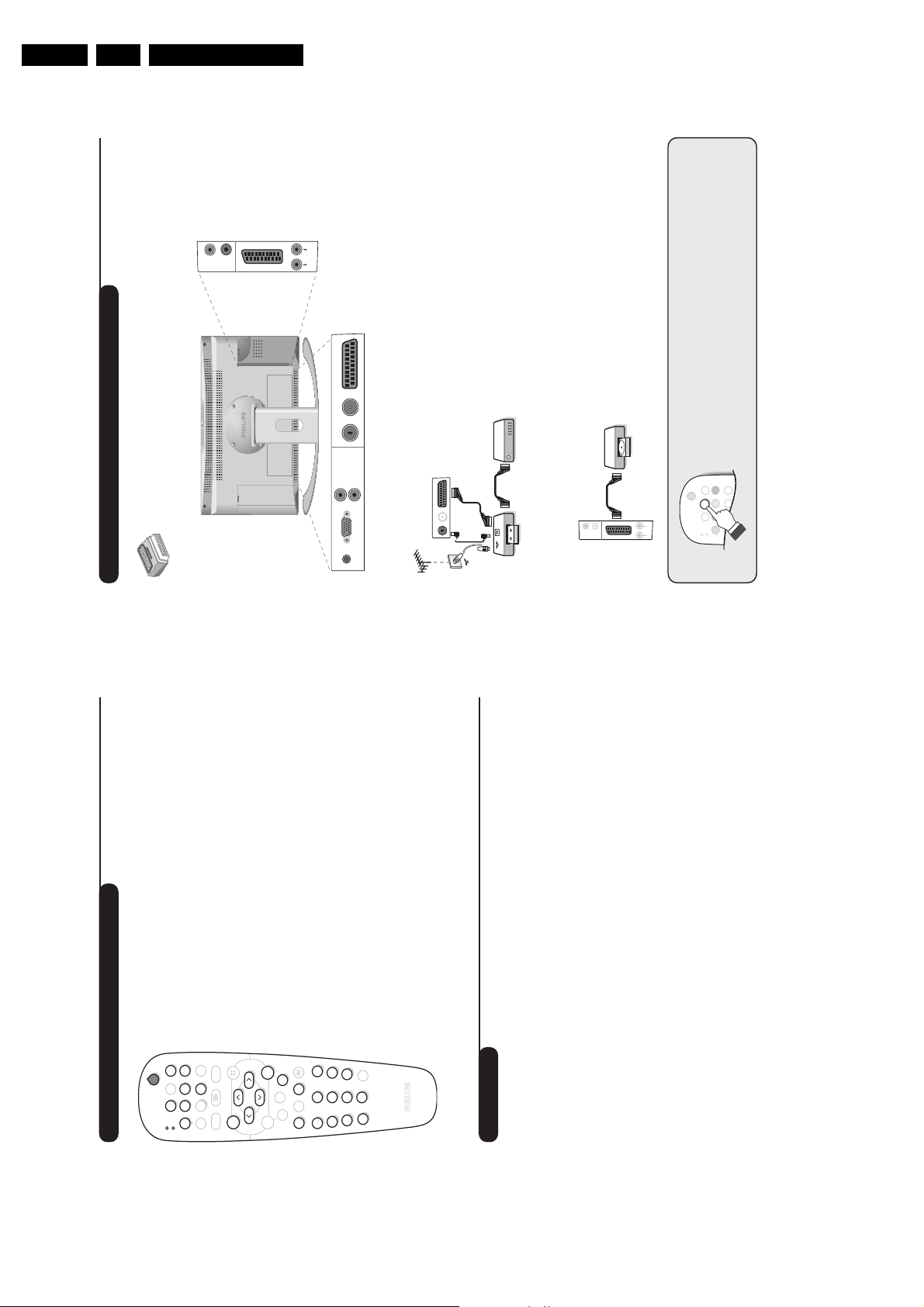
The
AV
and
S-VIDEO
connections are located under the
left panel or,for large screen sizes, under the right panel.
Make the connections as shown opposite.With the
n
key,
select
EXT3
.
For a monophonic device, connect the audio signal to the
AUDIO L input.The sound automatically comes out of the left
and right speakers of the set.
When headphones are connected, the sound on the TV set will
be cut.The
@
P
#
keys are used to adjust the volume level.
The headphone impedance must be between 32 and 600 Ohms.
Camcorder, video games
Headphones
O
To connect a Hi-fi unit use an audio connection cord and
connect the
L
and
R Audio out
of the TV to an
Audio in L
and
R
from the Hi-fi unit. If you have an active speaker
connect the
Subwoofer out
of the TV to the
Subwoofer in
of the speaker.
Connect the monitor output of your computer to the
PC
input (VGA)
of the TV. Connect the sound output
Audio out
L
and
R
of the computer to the input
Audio in (PC) L
and
R
of the TV.
For more information on using PC mode see page 8.
Configure the computer on 1280 x 1024, 60 Hz for
optimum resolution.
Attention:
if you use another resolution, the PIP function may not
work. In this case a warning message is displayed on the screen.
Here is the list of the different display resolutions available
on your TV:
640 x 350, 70 Hz 720 x 400, 70 Hz 1024 x 768, 60 Hz
640 x 350, 85 Hz 720 x 400, 85 Hz 1024 x 768, 70 Hz
640 x 480, 60 Hz 800 x 600, 56 Hz 1024 x 768, 75 Hz
640 x 480, 67 Hz 800 x 600, 60 Hz 1024 x 768, 85 Hz
640 x 480, 72 Hz 800 x 600, 72 Hz 1152 x 864, 75 Hz
640 x 480, 75 Hz 800 x 600, 75 Hz 1280 x 960, 60 Hz
640 x 480, 85 Hz 800 x 600, 85 Hz 1280 x 1024, 60 Hz
832 x 624, 75 Hz 1280 x 1024, 75 Hz
Amplifier
Computer
EN 13LC03E 3.
VIDEO
AUDIO
S-VIDE
L
R
R
out
Sub
L
woofer
*
out
Audio
Sub
woofer
in
*
out
Sub
woofer
in
Audio
LR
out
Audio
R
L
Audio in (PC)
PC input
Page 14
EN 14 LC03E4.
Mechanical Instructions
4. Mechanical Instructions
Index of this chapter:
1. Service Position
2. Stand Removal
3. Rear Cover Removal
4. Shield Removal
5. I/O Assy Removal
6. LED/Remote Control Board Removal
7. TV Board Removal
8. Scaler Board Removal
9. Inverter Board Removal
10. Top Control Assy Removal
11. LCD Panel Removal
12. Re-assembly
Note: Figures below can deviate from the actual situation, due
to different set executions.
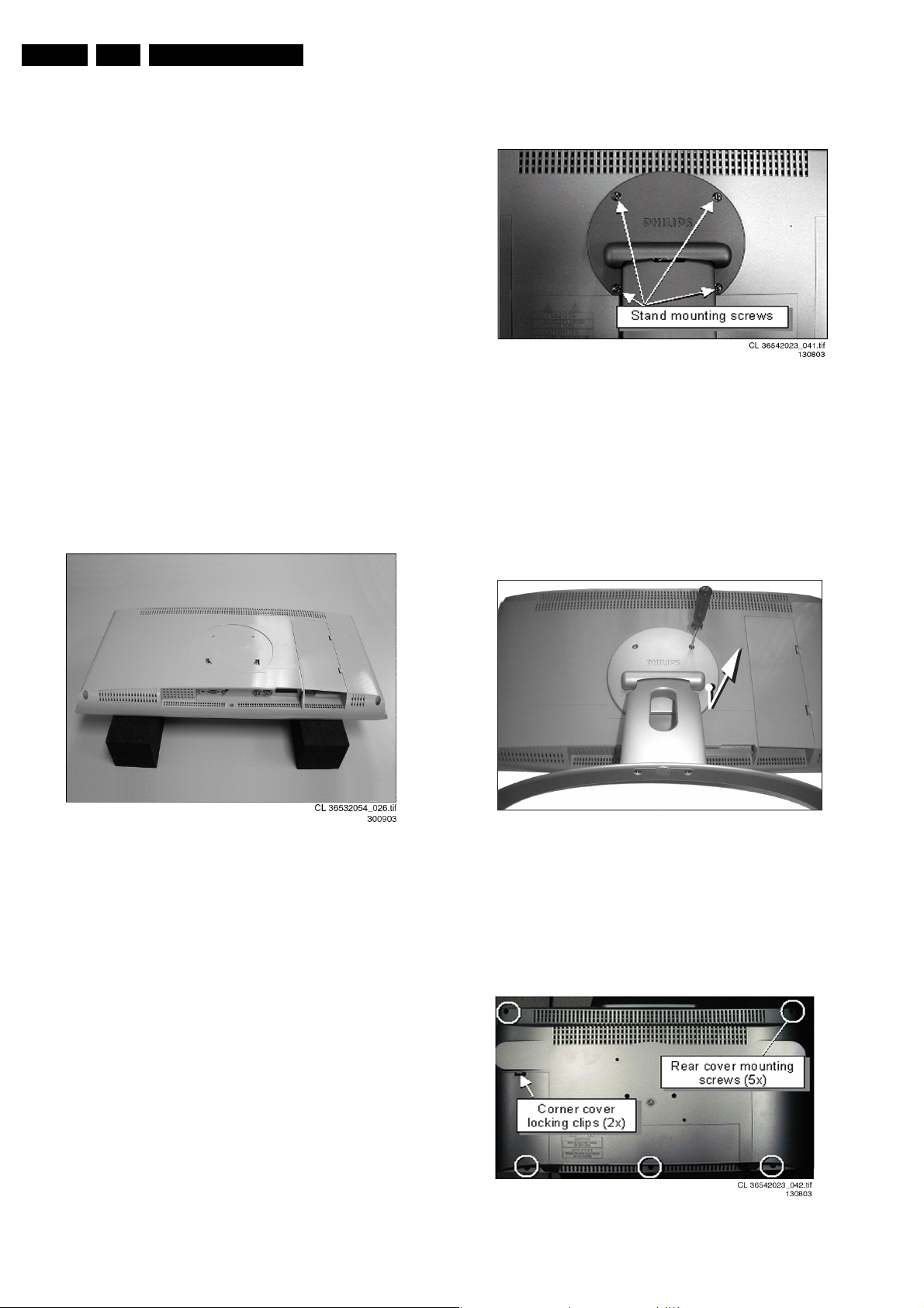
Figure 4-2 TV stand removal 15”/17” model
4.1 Service Position
First, put the TV in its service position. Therefore place it upside
down on a tabletop (use a protection sheet or a foam cushion).
Take care that this is flat and free from obstacles like screws,
to prevent damaging the fragile LCD screen.
ESD protective service buffers, as shown below, can be used
(3122 785 90580).
Figure 4-1 ESD protective service buffers
4.2.2 For 23 inch model
1. Use a Torx screwdriver to remove the stand from the
backside of the monitor housing by unscrewing the four
M4x12 mounting screws.
2. Remove the four mounting screws out of their mounting
holes.
3. First push the stand in horizontal direction to the monitor
bottom side, then lift the stand and take it away.
Figure 4-3 TV stand removal 23” model
CL 36532044_001.eps
160503
4.2 Stand Removal
4.2.1 For 15/17 inch model
Use a Torx screwdriver to remove the stand from the backside
of the monitor housing by unscrewing and removing the four
M4x12 mounting screws and next, take away the stand.
4.3 Rear Cover Removal
4.3.1 For 15/17 inch model
Manually unlock and remove both corner cover caps.
Figure 4-4 TV rear cover removal 15”/17” model
Page 15

Continue with the paragraph 4.3.3.
Mechanical Instructions
EN 15LC03E 4.
4.3.2 For 23 inch model
Manually unlock and remove the IO connector cover cap.
Connector cover cap
Figure 4-5 TV rear cover removal 23” model
4.3.3 For all models
1. Make sure all power-, audio-, video-, coax-, and SCART
cables are unplugged.
2. Remove the five Torx screws securing the monitor rear
cover.
3. Carefully remove the rear cover and store it on a safe
place.
CL 36532044_002.eps
160503
VGA connector distance screws
Figure 4-8 VGA Connector screws
• Remove all shield mounting screws.
CL 36532044_006.eps
160503
4.4 Shield Removal
• Remove at the “SCART plug side” the screw besides the
plug.
• Remove the connector plate.
Connector plate screws
Figure 4-6 TV SCART plug side
• Unscrew, at the bottom side, the connector plate screw and
remove this plate.
Connector plate screws
CL 36532044_003.eps
CL 36532044_004.eps
160503
160503
Figure 4-9 Shield with mounting screws
• Bend at the ”SCART-plug side” the thin metal electrostatic
shield away from the sockets, so the complete shield can
be lifted later on.
Electrostatic shield
CL 36532044_007.eps
Figure 4-10 Shielding
• Unlock the shield by carefully moving it a few millimetres to
the bottom side of the monitor. The topside of the shield
has to detach from underneath the two lock clamps, which
secure the shield at topside. Carefully lift the shield with
respect for the cables and/or connector sockets. Take out
the shield and store it on a safe place.
160503
Figure 4-7 Bottom side connector plate
• Use a 5 mm socket screwdriver to remove both connector
distance bolts from the “PC input / VGA-in” socket.
Page 16
EN 16 LC03E4.
Mechanical Instructions
4.5 I/O Removal
4.5.1 Side I/O assy removal for 15/17 inch model
Figure 4-11 Side I/O assy removal for 15”/17” model
1. Disconnect the cable connector [0240] from the side I/O
assy.
2. Unlock this unit by shifting it one centimetre to the outside
direction of the monitor.
3. Take out this side I/O assy.
2. To completely remove the Front LED panel (incl. Lens),
remove the assy screw.
4.7 TV Board Removal
4.7.1 For 15 /17inch model
Disconnect all five TV board connectors out of the regarding
sockets [3225], [1234], [1231], [1902], and [1732].
Continue with the paragraph 4.7.3.
4.7.2 For 23 inch model
Disconnect all six TV board connectors out of the regarding
sockets [3225], [1233], [1231], [1902], [1732] and [1734].
Continue with the paragraph 4.7.3.
4.7.3 For all models
1. Pull the thin flat cable out of its special shaped connector,
[1010].
2. Unscrew and remove the three TV board mounting screws.
3. Take out the TV board.
4.5.2 Side I/O assy removal for 23 inch model
Side I/O Assy
Figure 4-12 Side I/O assy removal for 23” model
1. Disconnect the cable connector [0240] from the side I/O
assy.
2. Unlock this unit by pushing it one centimetre in horizontal
direction (to bottom side) of the monitor.
3. Take out this side I/O assy.
4.6 Front LED Panel Removal
CL 36532044_008.eps
021003
CL 36532044_012.eps
160503
Figure 4-13 TV board
Note: Sometimes it is necessary to place the TV board in its
service position, for easy signal measuring. See picture below.
4.6.1 Only for the 23 inch model
To gain access to the Front LED panel unscrew and remove
the three mounting screws from the loudspeaker box covering
the panel. Release cables and take out the loudspeaker box.
Continue with the paragraph 4.6.2.
4.6.2 For all models
1. Unlock the transparent securing clip, which holds the Front
LED panel in place, and take out the Front LED panel .
(See previous figure: “Side IO assy removal for 15”/17”
model).
CL 36532044_010.eps
CL 36532044_010.eps
Figure 4-14 TV board in service position
160503
160503
Page 17

4.8 Scaler Board Removal
1. Carefully disconnect the cable connector in the centre of
the Scaler board [1506]. Take care not to damage the
fragile cables.
2. Disconnect the cable connectors at the edge of the Scaler
board [1402] and [1003].
3. Pull the thin flat cable out of its special shaped connector
[1681].
4. Unscrew and remove two Scaler board mounting screws.
5. Take out the Scaler board.
Figure 4-15 Scaler board
Mechanical Instructions
CL 36532044_013.eps
160503
EN 17LC03E 4.
2
1
Heat sink
CL 36532044_014.eps
Figure 4-17 Heat Sink Removal
4.9 Inverter Board Removal (only for 15/17 inch model)
Note: The Inverter board is available in two versions: one
model for TN-displays and another model for IPS-displays. The
(dis)assembly procedure is the same for both versions.
1. Disconnect the cable from the Inverter board.
2. Disconnect at top and bottom side all the black/white and
pink cable connectors.
3. Use a pair of pliers to bend the metal securing clamp in
such a way that the Inverter board can be taken out.
4. Remove the Inverter board and store it on a safe place.
160503
Note: Sometimes it is necessary to place the Scaler board in a
service position. In this case it is necessary to use the specific
“Repair kit scaler board” including two extra long cables (order
nr. 3122 785 90490).
CL 36532044_011.eps
Figure 4-16 Scaler board in service position
Important: Video converter chip heat sink.
1. Before you de-solder the video converter chip SAA7118
from the board, the heat sink must be removed from the
chip. Use a pair of pliers to remove the heat sink by means
of a twist- and pull movement (see figure). Store the heat
sink on a safe place, adhesive side up!
2. Place the self-adhesive heat sink back in place after the
chip exchange action has been finished.
160503
Figure 4-18 Inverter board
4.10 Top Control Assy Removal
1. Remove the cable from the Top control assy [1500].
2. Remove both mounting screws that secure the Top control
assy to the monitor frame.
3. Take out the Top control assy.
Page 18
EN 18 LC03E4.
Mounting screw(2x)
Mechanical Instructions
Figure 4-19 Top control assy
4.11 LCD Panel Removal
4.11.1 For 15 /17 inch model
Note: the LCD Panel is available in two versions: a TN-display
and an IPS-display. The (dis)assembly procedure is the same
for both versions.
1. Unscrew and remove the four LCD panel frame mounting
screws, which secure the panel frame to the monitor front.
2. Disconnect at both sides the speaker cable plugs and
remove the speaker cable assy.
3. Lift and take out the LCD panel (including its frame).
CL 36532044_015.eps
160503
Figure 4-21 LCD frame mounting screws 23” model
4.11.3 For all models
1. Remove the plastic monitor front from the protection sheet
and place the LCD panel, including the panel frame, back
on the protection sheet or foam cushion. Make sure again
that there are no screws or other parts left behind on the
protection sheet, that can damage the fragile panel screen
surface.
2. Unscrew the four screws, securing the panel frame to the
LCD panel (see figures: “LCD panel mounting screws”).
3. Take off the panel frame while leading the panel connector
through the access hole in the frame.
CL 36532044_016.eps
160503
Figure 4-20 LCD frame mounting screws 15”/17” model
Continue with the paragraph 4.11.3
4.11.2 For 23 inch model
1. To gain access to whole LCD Panel, unscrew and remove
the mounting screws from both Loudspeaker boxes.
Release cables and take out both Loudspeaker boxes.
Note: Avoid unscrewing screws from the Loudspeaker boxes
sockets, if you don’t want to disassemble the Loudspeaker
boxes.
1. Unscrew and remove the eight LCD frame mounting
screws, which secure the panel frame to the monitor front.
2. Lift and take out the LCD panel (including its frame).
Figure 4-22 LCD Panel mounting screws, 15”/17” model
LCD frame screws (4x)
Figure 4-23 LCD panel mounting screws, 23” model
4.12 Re-Assembly
To re-assemble the whole set, do all processes in reverse
order.
Notes:
• When you secure the panel frame (with the LCD panel) in
the monitor front, do not mount the fifth screw in the middle
CL 36532044_017.eps
011003
Page 19

Mechanical Instructions
of the bottom side. You will need this screw position for
mounting the TV rear cover.
• Take extra care when fixing the connector bracket screw at
SCART plug side. You can easily damage the TV board
when you use too much force.
• Do not forget to re-place the ground cable of the Scaler
board when mounting the screw at topside.
• Take extra care when reconnecting the Inverter board
backlight connectors (black/white/pink). Connect them
properly to avoid “high voltage sparking”
EN 19LC03E 4.
Page 20

EN 20 LC03E5.
Service Modes, Error Messages, and Repair Tips
5. Service Modes, Error Messages, and Repair Tips
Index of this chapter:
1. Test Points
2. Service Modes
3. Errors
4. The “Blinking LED” Procedure
5. ComPair
6. Trouble Shooting Tips
5.1 Test Points
This chassis is equipped with test points in the service printing.
In the schematics test points are identified with a rectangle box
around Fxxx or Ixxx. On the PCB, test points are specifically
mentioned in the service manual as “half moons” with a dot in
the centre.
Measurements are performed under the following conditions:
• Video: colour bar signal.
• Audio: 3kHz left, 1kHz right.
5.2 Service Modes
5.2.1 Limited DST Support
This chassis does still have some limited Dealer Service Tool
(DST) support, although this remote is not for sale anymore.
The set can be put in two service modes via the DST (RC7150).
These are the Service Default Mode (SDM) and the Service
Alignment Mode (SAM).
Installation Features Dealer
For easy installation and diagnosis the DST can be used.
When there is no picture (to access the error code buffer via the
OSD), DST can enable the functionality of displaying the
contents of the entire error code buffer via the blinking LED
procedure.
The dealer can use the RC7150 for programming the TV-set
with presets. Ten different program tables can be programmed
into the DST via a GFL or MG TV-set (downloading from the
GFL or MG to the DST; see GFL or MG service manuals) or by
the DST-I. For explanation of the installation features of the
DST, the directions for use of the DST are recommended.
5.2.2 Service Default Mode (SDM)
Purpose of SDM:
• To provide a situation with predefined settings to get the
same measurements as in this manual.
• To start the “Blinking LED” procedure.
• To have the possibility to override the 5V protection
Activating SDM:
• By transmitting the "DEFAULT" command with the RC7150
Dealer Service Tool (this works both while the set is in
normal operation mode or in the SAM).
• Standard RC sequence 0-6-2-5-9-6 followed by pressing
the “MENU”-button (this works both while the set is in
normal operation mode or in the SAM).
• By shorting pins 5 and 6 of connector 1170 of LED/RC
panel. Then apply DC supply from the AC-DC adaptor (not
required to remove the metal shielding).
Note: By temporarily shorting pins 5 and 6 of connector 1170
and then applying DC supply from the AC-DC adaptor, the 5V
protection is disabled.
Caution: Overriding the 5V protection should only be used for
a short period of time. In case of S/W protections (error 4) the
set will shutdown after 15 sec.
For recognition, “SDM” is displayed at the upper right corner of
the screen.
SDM Menu
TYPE: 17PF9945/012 HRS:0029
SWID: LC03E21-1.11 S317 1.03
ERR : 0 0 0 0 0 0 0
OPT : 79 254 14 56 128 000
Figure 5-1 SDM Menu
Deactivating SDM:
• Press the “EXIT”-button on the DST, or
• Press 0-0 on the standard RC, or
• Switch the set to Standby (the error buffer is NOT cleared).
Note: When the mains power is switched off while the set is in
SDM, the set will switch to SDM immediately when the mains
is switched on again.
The SDM sets the following pre-defined conditions:
• PAL/SECAM sets: tuning at 475.25 MHz PAL.
• NTSC sets: tuning at channel 3 (61.25 MHz).
• Volume level is set to 25% (of the maximum volume level).
Other picture and sound settings are set to 50%.
The following functions are switched off in SDM (and after
leaving SDM):
• Timer.
• Sleep timer.
The following functions are disabled during SDM (and enabled
after leaving SDM)
• Parental lock.
• Blue mute.
• Hospitality Mode.
• No-ident Timer (normally the set is automatically switched
off when no video signal (IDENT) was received for 15
minutes).
All other controls operate normally.
Special Functions SDM
Access to normal user menu
Pressing the “MENU” button on the remote control switches
between the SDM and the normal user menus (with the SDM
mode still active in the background).
Channel search
Pressing the “P+” button of the remote control will select the
next available channel in the preset list.
Type nr, Error buffer, etc
Pressing the “OSD” or “info+” button of the remote control
shows/hides the type nr, error buffer, SW ID, Hours and option
codes. OSD can be hidden to prevent interference with
waveform measurements.
SDM
CL 36532023_084.eps
110403
Page 21

Service Modes, Error Messages, and Repair Tips
EN 21LC03E 5.
Access to SAM
By pressing 0-6-2-5-9-6 “info+” (or OSD) in sequence on the
standard RC will switch from SDM to SAM.
5.2.3 Service Alignment Mode (SAM)
Purpose of SAM:
• To do alignments.
• To change option settings.
• To display/clear the error code buffer values.
Activating SAM:
• By transmitting the "ALIGN" command with the RC7150
Dealer Service Tool (this works both while the set is in
normal operation mode or in the SDM).
• Standard RC sequence 0-6-2-5-9-6 followed by pressing
the “info+”-button (this works both while the set is in normal
operation mode or in the SDM).
Deactivating SAM:
• Press the “EXIT”-button on the DST, or
• Press 0-0 on the standard RC, or
• Switch the set to Standby (the error buffer is NOT cleared).
Note: When the AC-DC adaptor power is switched off while the
set is in SAM, the set will go back to normal mode of operation
when the AC-DC adaptor is switched on again.
In SAM the following information is displayed on the screen:
SAM Menu
TYPE: 17PF9945/012 HRS:0029
SWID: LC03E21-1.11 S317 1.03
ERR : 0 0 0 0 0 0 0
OPT : 79 254 14 56 128 000
CLEAR ERRORS
OPTIONS
TUNER
WHITE TONE
GEOMETRY
SOUND
SMART SETTING
Figure 5-2 SAM Menu
• Operation hours timer (hexadecimal).
• Software identification of the main micro controller of TV-
board (LC03BBC-X.YY), and (S3DD E.FF) is the software
identification for micro-P of Scaler board:
– LC03 is the chassis name for LCD-TV launched in
2003.
– BBC is 1 letter and 2 digit combination to indicate the
regional software type and the supported languages.
– X = main version number.
– YY= subversion number.
– S3 = Scalar board used in 2003.
– DD = screen size of the LCD panel.
– E = main version number.
– FF = subversion number.
• Error buffer (7 errors possible).
• Option bytes (8 codes possible), summary of options are
explained below.
• Sub menus are listed in a scroll-menu.
SAM
CL 36532023_083.eps
160403
• Change the value of the selected menu item (e.g.
HOR.SHIFT).
• Activate the selected submenu (e.g. ASBY ON/OFF).
• To return to the main menu / previous menu, press “MENU”
keys on the remote control
Access to Normal User Menu
Pressing the “MENU” button on the remote control switches
between the SAM and the normal user menus (with the SAM
mode still active in the background). Pressing the “MENU” key
in a submenu will go to the previous menu.
Menus and Submenus
CLEAR ERRORS: Erasing the contents of the error buffer.
Select the CLEAR ERRORS menu item and press the MENU
RIGHT key. The content of the error buffer is cleared.
The functionality of the OPTIONS and ALIGNMENTS (TUNER,
WHITE TONE, GEOMETRY, SOUND and SMART SETTING)
sub menus are described in chapter 8.
5.2.4 Customer Service Mode (CSM)
This chassis is equipped with the “Customer Service Mode”
(CSM, like in the A10-chassis). CSM is a special service mode
that can be activated and deactivated by the customer, upon
request of the service technician/dealer during a telephone
conversation in order to identify the status of the set. This CSM
is a 'read only' mode therefore modifications in this mode are
not possible.
Activating Customer Service Mode.
The Customer Service Mode can be switched on:
• By pressing RC button is sequence “1-2-3-6-5-4” or,
• By pressing simultaneously the MUTE button on the
remote control and any key on the TV control buttons (P+,
P-, VOL +, VOL -) for at least 4 seconds.
When the CSM is activated:
• Picture and sound settings are set to nominal levels.
• Modes that interfere with the behaviour of the set are
switched off (sleep timer, auto standby, etc.).
• Pressing cursor DOWN “v” on the RC will switch to CSM2
screen if it is in CSM1 screen. Likewise pressing cursor UP
“^” will switch to previous CSM1 screen.
• Pressing “P+” or “P-“ on RC will select next available
channel to be displayed.
• Pressing channel numeric keys on RC will select the
desired channel to be displayed.
Deactivating Customer Service Mode.
The Customer Service Mode will be switched off after:
• Pressing any key on the remote control handset (except
“P+”, “P-” and cursor up/down)
• Switching off the TV set with the mains switch.
All settings that were changed during activation of CSM are
restored to the initial values.
Customer Service Mode Information Screen
After activating the Customer Service Mode the following
screen will appear.
SAM Menu Control
Menu items can be selected with the cursor UP/DOWN key.
The selected item will be highlighted. When not all menu items
fit on the screen, moving the cursor UP/DOWN will display the
next/previous menu items.
With the cursor LEFT “<” / RIGHT “>” keys, it is possible to:
• Activate the selected menu item (e.g. GEOMETRY).
Page 22

EN 22 LC03E5.
1 TYPE: 17PF9945/012 HRS:0029 CSM1
2 SWID: LC03E21-1.11 S317 1.03
3 ERR : 0 0 0 0 0 0 0
4 OPT : 79 254 14 56 128 000
5
6 SYSTEM: WEST EUR
7 NO SIGNAL
8 TIMER ON
9 CHANNEL BLOCKED
10 NOT PREFERRED
11 SOURCE : 5
12 SOUND : MONO
13 VOLUME : 26
14 BALANCE: 1
15 COLOUR : 50
Service Modes, Error Messages, and Repair Tips
CL 36532023_085.eps
Figure 5-3 CSM 1
The Customer Service Menu (CSM1) shows the following
information:
• Line 1: “TYPE: 99XX9999/99XHRS: nnnn”. TYPE: typeversion/model of the set (i.e. 17PF9945/12). HRS:
Hexadecimal counter of operating hours. (Standby hours
are counted as operating hours).
• Line 2: “SWID: AAAABBC-X.YYS3DDE.FF”. SWID:
(Software identification of the main micro controller on TVBoard and Scaler board) See paragraph “Service
Alignment Mode (SAM)”. Details on available software
versions can be found in the chapter “Software Survey” of
the publication “Product Survey - Colour Television”.
• Line 3: “CODES: xx xx xx xx xx xx xx ”. Error code buffer
(see paragraph “Errors”). Displays the last 7 errors of the
error code buffer.
• Line 4: “OPT xxx xxx xxx xxx xxx xxx xxx xxx”. Option
bytes. Option bits control the software and hardware
functionality of the chassis. An option byte or option
number represents 8 of those bits. Each option number is
displayed as a decimal number between 0 and 255. The
set may not work correctly when an incorrect option code
is set. See chapter 8 for more information on correct option
settings
• Line 6: “SYSTEM: EUROPE/WEST EUR/EAST EUR/UK/
FRANCE”. Indicates which colour and sound system is
installed for this preset as defined in the Manual INSTALL
menu:
– PAL BG
– PAL I
– PAL DK
– SECAM BG
– SECAM DK
– SECAM LL’
• Line 7: “NO SIGNAL”. Indicates that the set is not receiving
an “ident” signal on the selected source.
– No or bad antenna signal; connect a proper antenna
signal
– Antenna not connected; connect the antenna
– No channel / preset is stored at this program number;
go to the INSTALL menu and store a proper channel at
this program number
– The tuner is faulty (in this case the CODES line will
contain number 13); check the tuner and replace/repair
if necessary
Note: On some models, BLUE MUTE is displayed (if the BM
option is ON) when no signal is received.
• Line 8: “TIMER ON”. Indicates that the sleep timer is
activated. Complaints that may be caused by the activation
of the sleep timer.
• Line 9: “CHANNEL BLOCKED”. Indicates that one or more
channels are locked except the selected channel.
Complaints that may be caused by locked channels:
– TV cannot be switched on from standby with the local
keyboard buttons
– “P+” and “P-“ buttons on local keyboard do not function
To disable the LOCK feature:
140403
1. Select ”FEATURE” menu (with the Remote Control)
2. Select “LOCK” (with the RC)
3. Set to “OFF”
• Line 10: “NOT PREFERRED”. Indicates that the current
channel is not in the preferred channel list (by default, all
channels are skipped. A channel can be added as a
selected channel to the list of preferred channels:
1. Select “INSTALL” menu
2. Select “CHANNEL EDIT”
3. Select “ADD/DELETE”
4. Set to “ADD” with the left/right cursor keys
• Line 11: “SOURCE”. Indicates which SOURCE is installed
for this preset: EXT1, SVHS2, EXT2, or Tuner.
• Line 12: “SOUND”. Indicates which sound mode is installed
for this preset: Mono, NICAM, Stereo, L1, L2, SAP, Virtual,
or Digital.
• Line 13: “VOLUME”. Value indicates level at entry CSM.
• Line 14: “BALANCE”. Value indicates level at entry CSM.
• Line 15: “COLOUR”. Value indicates level at entry CSM.
1 TYPE: 17PF9945/012 HRS:0029 CSM2
2 SWID: LC03E21-1.11 S317 1.03
3 ERR : 0 0 0 0 0 0 0
4 OPT : 79 254 14 56 128 000
5
6 BRIGHTNESS: 50
7 CONTRAST : 56
8 HUE : 50
9
10
11
12
13
14
15
Figure 5-4 CSM 2
The next Customer Service Menu (CSM2) shows the following
information:
• Line 6: “BRIGHTNESS”. Value indicates level at entry
CSM.
• Line 7: “CONTRAST”. Value indicates level at entry CSM.
• Line 8: “HUE”. Value indicates level at entry CSM.
• Line 9: “HOTEL MODE ON”. Indicates that the Hotel mode
has been activated.
5.3 Errors
5.3.1 Error Code Buffer
The error code buffer contains all errors detected since the last
time the buffer was erased. The buffer is written from left to
right. When an error occurs that is not yet in the error code
buffer, the error is written at the left side and all other errors
shift one position to the right.
The error code buffer will be cleared in the following cases:
– By activating the CLEAR ERRORS function in SAM menu.
– By transmitting 0-6-2-5-9-9 with the normal RC.
– By transmitting the commands “DIAGNOSE 99 OK” with
the DST (RC7150) or with ComPair.
– Automatically reset if its contents has not changed for 50
hours.
By leaving SDM or SAM with the mains switch, the error buffer
is not reset.
Examples:
ERROR: 0 0 0 0 0 0 0 : No errors detected
ERROR: 6 0 0 0 0 0 0 : Error code 6 is the last and only
detected error
ERROR: 9 6 0 0 0 0 0 : Error code 6 was first detected and error
code 9 is the last detected (newest) error
CL 36532023_086.eps
140403
Page 23
Service Modes, Error Messages, and Repair Tips
EN 23LC03E 5.
The contents of the error buffer can also be made visible
through the “blinking LED” procedure. This is especially useful
when there is no picture. See paragraph 5.4 “The blinking LED
procedure “.
5.3.2 Error Codes
In case of non-intermittent faults, clear the error buffer before
starting the repair, to prevent that “old” error codes are present
(it is wise to write down the content of the error buffer before
you clear it). If possible check the entire content of the error
buffers. In some situations an error code is only the result of
another error code (and not the actual cause).
Note: a fault in the protection detection circuitry can also lead
to a protection.
Table 5-1 Error codes
Error
Error description Possible defective
code
0 No error detected - ---1-3 Reserved
4 5V protection active IC7930 or +5V I2C
5 Reserved
6 General I2C bus er-
ror
7 Reserved
8 BOCMA I2C error IC 7301 A4
9 BOCMA 8V supply
failure
10 NVM I2C error IC 7066 A1
11 NVM identification
failure
12 uProcessor internal
RAM test failure
13 Tuner I2C error IC 1100 - UR13xx A3
14 Sound processor
I2C error
15 SRAM I2C error IC 7070 A2
16 Reserved
17# 3D CF processor
I2C error
18-20 Reserved
21 Scaler protection
active
22 Scaler protection
active
23 Scaler protection
active
24* HDTV decoder I2C
error
25 Scaler protection
active
26 Reserved
27 Scaler protection
active
28 Scaler protection
active
29 Scaler uP I2C error IC 7753 or IC 7064 C8, A1
* = Not applicable to Europe execution# = Only for NAFTA 23" execution
components
devices
I2C bus s/c or o/c
IC 7910 or IC7301 A4, A10
IC 7066 A1
IC 7064 A1
IC 7620 (MSP34xx) A8
IC 7823 B
IC 7402 C4
IC 7351 C9
IC 7302 C3
IC 7252 C10
IC 7752 C8
IC 7471 C6
IC 7472 C6
Diagram
A3, A8,
A10
TV-Board
Errors
• Error 0 = No error
• Error 4 = +5V protection. 5V protection active; set is
switched to protection; error code 4 is placed in the error
buffer; the LED will blink 4 times (repeatedly). A 5V failure
can cause a drop in the 5V supply output, resulting in an
undefined behaviour of the set. Therefore, all I2C devices
connected to the 5V supply are constantly monitored.
When none of these devices responds to the micro
controller for a prolonged time, the micro controller
assumes that there is a failure in the 5V supply. By starting
up the set with the service jumpers shorted, the 5V
protection is disabled and it is easier to determine the
cause. +5V protection will be activated when these I2C
devices fail (no I2C communication):
– Main Tuner 1100 (diagram A3)
– ITT sound processor MSP34xx IC-7620 (diagram A8)
Service tips: To isolate the problem area after overriding the
+5V protection, determine whether:
1. The +5V source is working properly IC7930 (diagram A10)
2. ITT sound processor circuit is loading the +5V; isolate coil
5620 (diagram A8)
3. The audio delay IC 7601 - IC7605 is loading the +5V
source; isolate coil 5601 (diagram A7)
4. Main tuner circuit is loading the +5V source; isolate coil
5122 (diagram A3)
Caution: Overriding the 5V protection when there is a 5V
failure can increase the temperature in the set and may cause
permanent damage to components. Do not override the 5V
protection for a prolonged time.
• Error 6 = General I2C error. This will occur in the following
cases:
– SCL or SDA is shorted to ground
– SCL is shorted to SDA
– SDA or SCL connection at the micro controller is open
circuit.
• Error 8 = BOCMA IC TDA888xx (diagram A4) I2C
communication failure. BOCMA (IC7301 on TV board) is
corrupted or the I2C line to the BOCMA is low or no supply
voltage present at pin 14 (3V3) or no supply voltage at pin
23.
• Error 9 = BOCMA IC TDA888xx 8V failure (SUP bit). No
supply voltage at pin 53. Check coil 5302.
• Error 10 = NVM I2C error (diagram A1). NVM (EEPROM IC7066) does not respond to the micro controller.
• Error 11 = Micro controller / NV Memory identification error.
During the last start-up the NVM and the micro controller
did not recognize each other (e.g. one of them was
replaced or the NVM memory has been changed/adapted
or lost), therefore the NVM was loaded with default values.
• Error 12 = Microprocessor (Painter - IC 7064) internal RAM
test failure.
• Error 13 =Main Tuner I2C failure UR13xx. Tuner (item
1100, diagram A3) is corrupted or the I2C line to the tuner
is low or no supply voltage at pin 3, pin 6 or 7 of the tuner.
• Error 14 =Sound processor I2C error IC7620 (MSP34xx,
diagram A8). Sound controller does not respond to the
micro controller.
• Error 15 =SRAM IC CY7C1019 test failure (IC7070,
diagram A2).
Note: Only for Europe and AP-PAL execution.
Scaler Board
When the TV detects critical errors from the Scaler board, it will
shutdown into protection mode. After a short period of time, the
LED will blink according to the respective error codes.
Page 24

EN 24 LC03E5.
Service Modes, Error Messages, and Repair Tips
Protection errors:
• Error 21 = JagASM processor test failure (IC7402, diagram
C4). During start-up of set, the Scaler will do a quick test by
writing data to selective addresses and reading back the
data. If the core supply voltage is too low or data line is
broken, this error protection will be activated. Under these
circumstances, check:
– Core supply of 2V5 to VDD pins of JagASM IC.
– Clock pulse present at pin 3 of OSC generator item
1401 (diagram C4).
• Error 22 = Video formatter/converter I2C error IC7351
(GENESIS FLI2300, diagram C9).
• Error 23 = Video decoder I2C error IC7302 (Philips
SAA7118E, diagram C3).
Note: BGA IC fixed with a heat sink (see chapter 4 how to
remove).
• Error 25 = NVM I2C error (diagram C8). NV memory
(EEPROM - IC7752) does not respond to Scaler micro
controller.
• Error 27 = SRAM IC MT48LC2M32B2TG test failure
(IC7471, diagram C6).
• Error 28 = SRAM IC MT48LC2M32B2TG test failure
(IC7472, diagram C6).
Non-Protection errors:
• Error 24 = HDTV decoder I2C error IC7252 (AD9883,
diagram C10).
Note: This error is NOT applicable to Europe execution.
• Error 29 = TV uP IC7064 (diagram A1) and Scaler uP
IC7753 (diagram C8) I2C communication failure. When this
error occurred, there is no display on screen. In order to
read this error code, either activate SDM or press “062501”
to read out the error code by blinking LED. Alternatively,
read the error codes out by using ComPair.
5.4 The “Blinking LED” Procedure
The contents of the error buffer can also be made visible
through the “Blinking LED” procedure. This is especially useful
when there is no picture.
When the SDM is entered, the LED will blink the contents of the
error-buffer. Error-codes ≥ 10 are shown by a long blink of
750msec, which is an indication of the decimal digit, followed
by a pause of 1500msec. followed by n short blinks. When all
the error-codes are displayed, the sequence is finished with a
LED display of 3 seconds. The sequence starts again.
Example:
Error code position: 1 2 3 4 5
Error buffer: 12 9 6 0 0
This gives after activating SDM: 1 long blink of 750msec +
pause of 1500msec + 2 short blinks - pause of 3 s - 9 short
blinks - pause of 3 s - 6 short blinks - pause of 3 s - long blink
of 3 s - etc.
Note: If errors 1, 2 or 4 occur, the LED always blinks the last
occurred error, even if the set is not in service mode.
Another method of reading out a single error code is to use a
standard RC or a DST.
• Standard RC - Press “0-6-2-5-0-x” in sequence, to read
(blinking LED) out a respective error code in the error
buffer, where x = 1, 2, 3, 4, 5, 6, or 7.
• DST: Press “Diagnose” “x” “OK” to read (blinking LED) out
a respective error code in the error buffer, where x = 1, 2,
3, 4, 5, 6, or 7.
5.5 ComPair
5.5.1 Introduction
ComPair (Computer Aided Repair) is a service tool for Philips
Consumer Electronics products. ComPair is a further
development on the European DST (Dealer Service Tool),
which allows faster and more accurate diagnostics. ComPair
has three big advantages:
ComPair helps you to quickly get an understanding on how to
repair the chassis in a short time by guiding you systematically
through the repair procedures.
ComPair allows very detailed diagnostics (on I2C level) and is
therefore capable of accurately indicating problem areas. You
do not have to know anything about I2C commands yourself
because ComPair takes care of this.
ComPair speeds up the repair time since it can automatically
communicate with the chassis (when the microprocessor is
working) and all repair information is directly available. When
ComPair is installed together with the SearchMan electronic
manual of the defective chassis, schematics and PWBs are
only a mouse click away.
5.5.2 Specifications
ComPair consists of a Windows based faultfinding program
and an interface box between PC and the (defective) product.
The ComPair interface box is connected to the PC via a serial
or RS232 cable.
The ComPair faultfinding program is able to determine the
problem of the defective television. ComPair can gather
diagnostic information in two ways:
• Automatic (by communication with the television):
ComPair can automatically read out the contents of the
entire error buffer. Diagnosis is done on I2C level. ComPair
can access the I2C bus of the television. ComPair can
send and receive I2C commands to the micro controller of
the television. In this way, it is possible for ComPair to
communicate (read and write) to devices on the I2C
busses of the TV-set.
• Manually (by asking questions to you): Automatic
diagnosis is only possible if the micro controller of the
television is working correctly and only to a certain extend.
When this is not the case, ComPair will guide you through
the faultfinding tree by asking you questions (e.g. Does the
screen show a picture? Click on the correct answer: YES /
NO) and showing you examples (e.g. Measure test-point I7
and click on the correct waveform you see on the
oscilloscope). You can answer by clicking on a link (e.g.
text or a waveform picture) that will bring you to the next
step in the faultfinding process.
By a combination of automatic diagnostics and an interactive
question / answer procedure, ComPair will enable you to find
most problems in a fast and effective way.
Beside fault finding, ComPair provides some additional
features like:
• Up- or downloading of pre-sets.
• Managing of pre-set lists.
• Emulation of the Dealer Service Tool (DST).
• If both ComPair and SearchMan (Electronic Service
Manual) are installed, all the schematics and the PWBs of
the set are available by clicking on the appropriate
hyperlink. Example: Measure the DC-voltage on capacitor
C2568 (Schematic/Panel) at the Mono-carrier.
– Click on the 'Panel' hyperlink to automatically show the
PWB with a highlighted capacitor C2568.
– Click on the 'Schematic' hyperlink to automatically
show the position of the highlighted capacitor.
Page 25
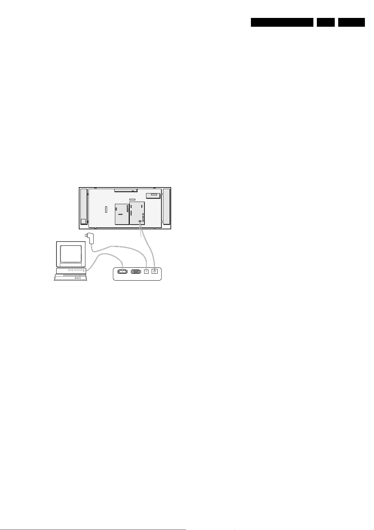
Service Modes, Error Messages, and Repair Tips
EN 25LC03E 5.
5.5.3 How To Connect
1. First, install the ComPair Browser software (see the Quick
Reference Card for installation instructions).
2. Connect the RS232 interface cable between a free serial
(COM) port of your PC and the PC connector (marked with
'PC') of the ComPair interface.
3. Connect the mains adapter to the supply connector
(marked with 'POWER 9V DC') of the ComPair interface.
4. Switch the ComPair interface 'OFF'.
5. Switch the television set 'OFF' with the mains switch.
6. Connect the ComPair interface cable between the
connector on the rear side of the ComPair interface
(marked with 'I2C') and the ComPair connector inside the
TV (the ComPair connector (pos.nr.1111) is situated close
to the tuner on the TV Board, see Chassis Overview in
chapter 1).
7. Plug the mains adapter in a mains outlet, and switch the
interface 'ON'. The green and red LEDs light up together.
The red LED extinguishes after approx. 1 second while the
green LED remains lit.
8. Start the ComPair program and read the 'Introduction'
chapter.
LCD PANEL
To LCD
Speaker assy R
To Inverter
ComPair
SERVICE
CONNECTOR
PC VCR I2CPower
9V DC
Figure 5-5 ComPair Interface connection
5.5.4 How To Order
ComPair order codes (EU/AP/LATAM):
• Starter kit ComPair32/SearchMan32 software and
ComPair interface (excl. transformer): 3122 785 90450.
• ComPair interface (excluding transformer): 4822 727
21631.
• Starter kit ComPair32 software (registration version): 3122
785 60040.
• Starter kit SearchMan32 software: 3122 785 60050.
• ComPair32 CD (update): 3122 785 60070 (year 2002,
3122 785 60110 (year 2003).
• SearchMan32 CD (update): 3122 785 60080 (year 2002),
3122 785 60120 (year 2003).
• ComPair interface cable: 3122 785 90004.
• ComPair firmware upgrade IC: 3122 785 90510 (only for
sets with software upgrade facilities).
• Transformer Europe: 4822 727 21632.
• Transformer UK: 4822 727 21633.
Note: If you encounter any problems, contact your local
support desk.
Speaker assy L
CL36532000_000.eps
011003
5.6 Trouble Shooting Tips
5.6.1 Scaler/TV Board Power Supply Problems
In this paragraph some troubleshooting steps for checking the
power supply of the Scaler-board and TV-board circuitry are
described.
• Measure across pin-1 and pin-4 of connector 1003
(diagram C1). +12V (15” and 17”) or +24V (23”) should be
present. If the voltage is not present, probably is caused
by:
– AC to DC adaptor is defect.
– Short circuit in TV-board (can be isolated by connector
1003).
– Fuse 1002 is open circuit.
• Measure across C2923 (diagram A10). +3V3 should be
present. If not present, probably this is caused by:
– IC7920 is defective.
– R3925 is defective.
– The power supply circuit (diagram C1) is defective (see
Scaler-board circuit trouble shooting tips).
• Measure R3017 or R3085 (diagram A1) with oscilloscope.
There should be I2C activity. If no activity is present, this
probably is caused by:
– IC 7064 micro-P is defective.
– The I2C clock line or data line is grounded. (LED
should blink indicating SW protection is active).
– The IC 7064 reset circuit consisting of T7063, T7067
and T7069 and its surrounding components are
defective.
• Measure pin-19 of connector 1010 (diagram A1). The
standby signal should be high (2V9). If not high, probably
this is caused by:
– IC 7064 micro-P is defective (output port pin-13).
– Transistor 7062 is defective.
• Measure across C2913/C2933 (diagram A10). +8V3/+5V4
should be present respectively. If not present, probably this
is caused by:
– IC 7910/7930 regulator is defective.
– Fuse 1903 is defective.
– Switching FET 7900 is defective.
– Transistor T7901 is defective.
• Measure across C2007 (diagram C1). +5V should be
present. If not present, probably this is caused by:
– +5V grounded by the load.
– Regulator IC 7001 is defective.
– Control transistor T7003/7002 is defective.
– Scaler power control signal line (POW-CON-SCALER
coming from TV-board) is defective.
• Measure pin-4 or pin-5 of connector 1402 (diagram C4).
Pin-4 should be high (+4V7) and pin-5 also should be high
(+3V4). If one/both of the voltage is not present, probably
this is caused by:
– IC 7402 (JagASM) is defective.
– Transistor 7403 is defective.
– Inverter board is defective.
• Measure pin-4 or pin-5 of connector 1402 (diagram C4).
Pin-4 should be high (+4V7) and pin-5 also should be high
(+3V4). If one/both of the voltage is not present, probably
this is caused by:
– IC 7402 (JagASM) is defective.
– Transistor T7403 is defective.
– Inverter board is loading either of the voltage.
Page 26

EN 26 LC03E5.
Service Modes, Error Messages, and Repair Tips
5.6.2 General Problems
TV switched “off” or changed channel without any user action
Set switches off after “TV SWITCHING OFF” was displayed.
“Auto Standby” switched the set “off” because:
• There was no ident signal for more than 15 minutes.
• There was no remote control signal received or local key
pressed for > 2 hours.
See chapter 8 for a description on the options to enable/disable
“Auto Standby”.
5.6.3 Picture Problems
Picture too dark or too bright
• Press “Smart Picture” button on the remote control. In case
the picture improves, increase / decrease the brightness
value or increase / decrease the contrast value. The new
“Personal Preference” value is automatically stored after 3
minutes.
• After switching on the Customer Service Mode the picture
is OK. Increase / decrease the brightness value or increase
/ decrease the contrast value. The new “Personal
Preference” value is automatically stored after 3 minutes.
Snowy picture
Check the “NOT TUNED” section of the Customer Service
Mode screen.
5. Select the STORE menu item
• When the set is in PC mode and there is no VGA signal
present at PC-in connector, the set will shutdown to
standby in couple of seconds after showing “NO VIDEO
INPUT”. This is a normal behaviour of the set to safe
power.
• The Scaler is the driving engine of the LCD panel. When
there is no display and OSD on screen, check whether
sound is producible on TV channel. If sound is audible,
most likely the defective lies in Scaler board or inverter
board.
• To know fast whether inverter is functioning, visually check
if the backlights are “on” by looking at the back of the LCD
panel. Some bright spots can be seen on the side. Other
way to tell whether the backlight is working is to switch the
set to AV mode. The front of the screen had some kind of
“fogged” effect.
Note: when one of the backlight connectors has loosened,
the inverter circuit will be shut down.
• If the supply to the LCD panel is OK (likewise for backlight
supply), but no data signals (example: signals on
connector 1506) supplied from Scaler to LCD panel, you
will notice that the LCD screen will shown full screen in
sequential of BLUE, GREEN, RED, BLANK, dark-GREY,
light-GREY and WHITE repeatedly. It means LCD panel is
in good condition. The fault lies in the Scaler board
Snowy picture and/or unstable picture
A scrambled or decoded signal is received.
Black and white picture
• Press “Smart Picture” button on the remote control. In case
picture improves, increase the colour value. The new
“Personal Preference” value is automatically stored after 3
minutes.
• After switching on the Customer Service Mode the picture
is OK. Increase the colour value. The new “Personal
Preference” value is automatically stored after 3 minutes.
Menu text not sharp enough
• Press “Smart Picture” button on the remote control. In case
the picture improves, decrease the contrast value. The new
“Personal Preference” value is automatically stored after 3
minutes.
• After switching on the Customer Service Mode the picture
is OK. Decrease the contrast value. The new “Personal
Preference” value is automatically stored after 3 minutes.
5.6.4 Sound Problems
No sound or sound too loud (after channel change / switching on)
After switching on the Customer Service Mode the volume is
OK. Increase / decrease the volume level. The new “Personal
Preference” value is automatically stored after 3 minutes.
5.6.5 Extra Information/Tips:
• Complaints that may be caused by an incorrect system
setting:
– No colours
– Colours not correct
– Unstable picture
– Noise in picture
To change the system setting of a preset:
1. Press the “MENU” button on the remote control
2. Select the INSTALL sub menu
3. Select the MANUAL STORE sub menu
4. Select and change the SYSTEM setting until
picture and sound are correct
Page 27
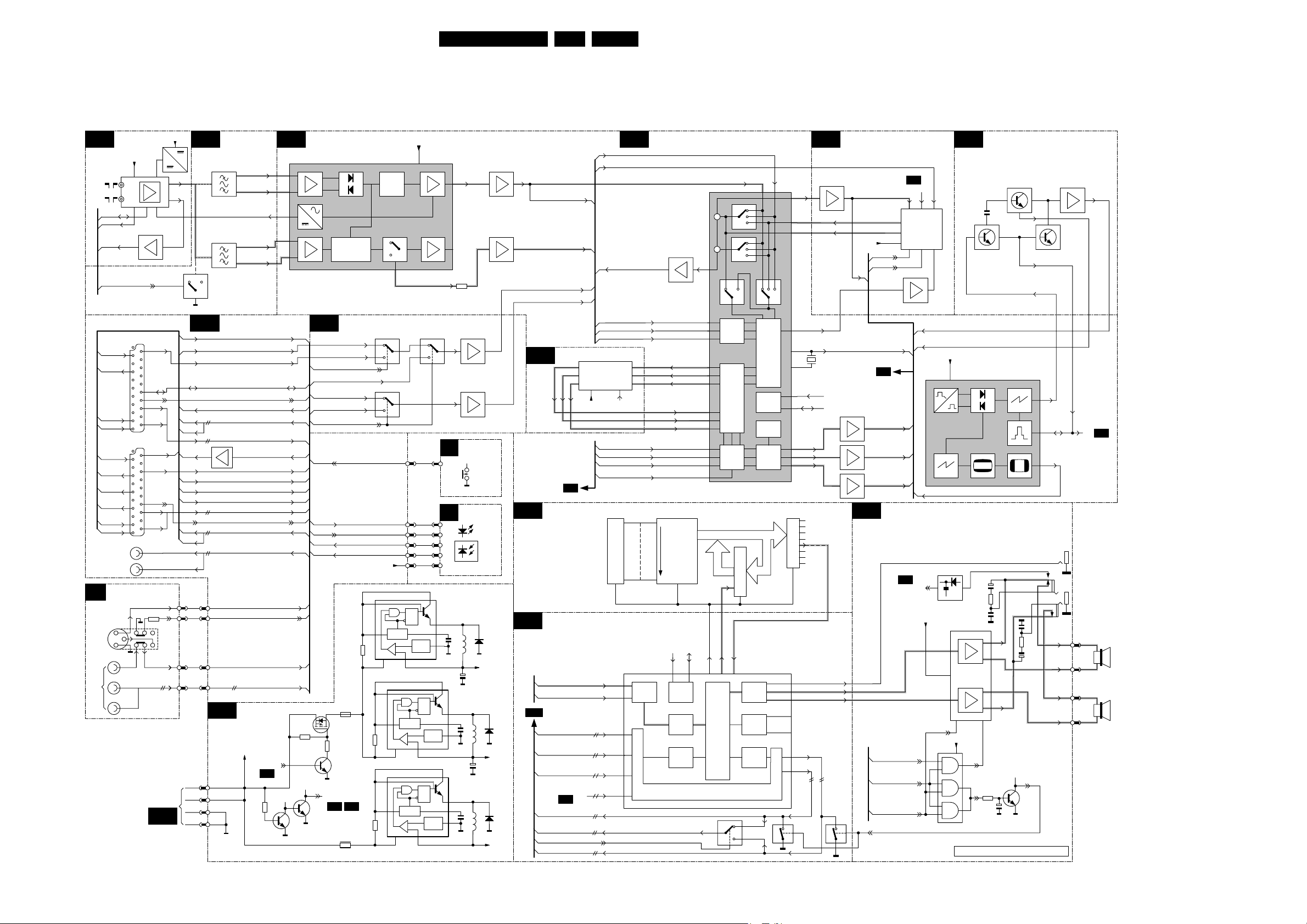
Block Diagrams, Testpoint Overviews, and Wiring Diagram
6. Block Diagrams, Testpoint Overviews, and Wiring Diagram
Block Diagram (Tuner-IF-Video)
27LC03E 6.
A 3
TV
FM
SDA-0
A1
SCL-0
A1
SIF-FM
A8
SEL-IF-LL_M-TRAP
A1
16
MON-Out
15
C-In
12
L-Out
11
R-Out
TER-Out
9
7
R-In
G-In
6
B-In
5
L-Out
2
R-Out
1
AUDIO-L OUT
AUDIO-R OUT
D
SVHS 2
VIDEO
AV3
TUNER
1100
SIDE AV
C
Y
L
R
+5V4
6,7,3
4
7130//7131
SCART 2
21
20
2
1
SCART 1
21
20
2
1
9
51
Y/CVBS-In
P50
Status
L-In
R-In
CVBS-In
FBL-In
Status
L-In
R-In
3242
TO/FROM
1003 OF
SCALER
BOARD
C 1
+5V4
11
10
10
6,8
VIDEO & QSS IF
A 5
1452
1454
7452
SCART IO
A 11
15
10
L
R
7224
L
R
1233
4
7
2
6,8
STATUS2_SVHS-RR-DET
EF
16
12
11
9
7
6
5
2
1
0204
4
7
2
A 10
12-24DC-SUP_1
1902
4
3
2
1
VIF1
8
VIF2
7
AGC
VSIF1
7
VSIF2
8
C-SC2_SVHS-IN
CVBS-SC1_AV1-IN
Y-CVBS-SC2_AV2-IN
COMM-LINE
CVBS-SC2_MON-OUT
LR-SC2-OUT
LR-SC2_AV2-IN
CVBS_TER_OUT
FBL-SC1-IN
R-SC1-IN_V-IN
G-SC1-IN_Y-IN
B-SC1-IN_U-IN
LR-SC1_AV1-IN
STATUS1
LR-SC1_AV-OUT
LR-CL_VL-OUT
C-FRONT-IN
SVHS-SIDE-DET
Y-CVBS-FRONT-IN
LR-FRONT-IN
LOCAL SUPPLY
STANDBY
A1
3904
7903
1
2
7
8
9
VDP - COLOUR PROCESSING
A 4
7301-A
A 5
A5
A1
A11
A1
A11
A1
A11
A4
A8
A1
A8
A4
A1
A4
A4
A4
A4
A8
A1
A1
A8
A1
A1
A8
A1
A5
A1
A5
A8
7900
3900
7901
7904
QSS Mixer
AM Demod.
EXT. VIDEO SELECT
SEL-MAIN-R1R2
Y-CVBS-FRONT-IN
C-SC2_SVHS-IN
C-FRONT-IN
SEL-MAIN-FRNT-RR
KEYBOARD
PC-TV-LED
STBY-LED
RC5
LIGHT-SENSOR_SDM
391x
1903
3901
POWER-DOWN
A1 A9
3925
5
3
12
13
8
7
393x
3921
7401-C
7401-A
+8V3
7910
VCC
8
7
8
7
Sound
Traps
9
11
6
7930
VCC
7920
VCC
OSC
VDP - COLOUR PROCESSING
+8V3A
23
16
27
11
7401-B
2
4
1
14
3308
15
10
7412-B
7412-A
7302
EF
(SCART)
CVBS_TER_OUT
7303
EF
MAIN-CBVS-EXT-IN
MAIN-C-EXT-IN
EF
EF
A 5
SIF-TV
HISTOGRAM
7403
14
19
18
+8V3A
A11
A11
A11
A11
HISTOGRAM
16
E
1234
2
1
3
4
6
7
S
OSC
6
OSC
6
1150
2
1091~4
A1
FRONT
J
INTERFACE
1170
1231
1
1008
3
4
6
7
1
Q
2
R
3
4
REF
5
1
Q
S
R
REF
5
1
Q
S
R
REF
5
1002
6910
2911
5911
+8V3
2913
2
3
4
2
3
4
2931
2921
2933
5931
5921
6930
+5V4
6920
+3V5
AUDIO DELAY (80ms)
A 7
AUDIO PROCESSING
A 8
SIF-TV 50
A4
SIF-FM 52
A3
A11
LR-SC1_AV1-IN
LR-SC2_AV2-IN
LR-FRONT-IN
PC-HDAUDIO-LR
A1
LR-CL_VL-OUT
LR-SC2-OUT
SEL-MAIN-R1R2
LR-SC1_AV-OUT
A 4
MAIN-CBVS-EXT-IN
MAIN-C-EXT-IN
A11
A8
CVBS-SC2_MON-OUT
R-SC1-IN_V-IN
G-SC1-IN_Y-IN
B-SC1-IN_U-IN
7
2
3
5
SC
R-TXT-OSD
G-TXT-OSD
B-TXT-OSD
FBL-TXT-OSD
7601/2 7603
8-BIT COUNTERS
11,13
7651
DEMODULATOR
44,45
41,42
38,39
36,35
7330
EF
Y-MAIN
U-MAIN
V-MAIN
Y-HISTOGRAM
U-HISTOGRAM
V-HISTOGRAM
A0
32KX8
STATIC
RAM
A13
27
SCL
I2C
INTERF
IDENT
D/A
7301-B
+
+
26
41
42
43
40
45
MATRIX
46
39
47
48
35
36
37
38
SDA
I2S_CLOCK
I2S_DATA_OUT
3
21
DSP
INPUT SWITCH
7680
14,15
RGB/
YUV
INT
RGB/
YUV
YUV
INTER-
FACE
SAT.
CTRL
RGB
INPUT
A0----A7
7604
2
I2S_DATA_IN
6
5
10,11
D-LATCH
1,11
D/A
D/A
D/A
2,12
1,13
COLOUR
DECOD-
ING
RGB/
YUV
MATRIX
I2C
BUS
CTRL
CAT.
CALIB.
RGB
OUTPUT
2924
7605
23
21
20
17
18
28,29
25,26
7678/9
54
21
20
49
52
51
17
18
33
32
31
4614
D-LATCH
1,11
COMB-ON
A 6
7427
1330
SCL
SDA
7350
7353
7356
AUD_SW
AUDIO-L
AUDIO-R
Y-IN
C-IN
ANALOG COMB FILTER
EF
+5V
CVBS-TXT-CC
CLOCK12MHZ
EF
EF
EF
A 9
A1
SOUND_ENABLE
POWER-DOWN
A10
STAND-BY
A1
7674/5
OUT_MUTE
SANDCASTLE1
7405
14
16
5,6
SYS1
SYS2
7428
A1
R-DRIVE
G-DRIVE
B-DRIVE
AUDIO AMP 2x3W
(15" & 17")
A1
HP-SIDE-DET
A5
1
7
12
COMB
FILTER
11 10
9
EF
C-SYNC
H-SYNC
7301-C
50/60Hz
V-SYNC
12-24DC-SUP_1
1
2
9
10
12
13
+8V3
53
G
7731
6
1
VCC
8
59
+3V5
7732
14
C-SYNC GENERATOR
A 5
7380~1 7382
2380
7390~1 7383~5
LINEDRIVE1
G
15625
TV
2750
3750
2751
+
-
-
+
VOLSTB
3
8
3743
2746
11
TV
2
4
10
12
Ver 1.0 Final 03-03-06
7744
56
57
64
2753
3752
2752
EF
SC
A5
(HISTOGRAM)
1733
EXT. SW
1731
HP
LEFT
4
3
1732
RIGHT
1
2
CL 36532023_003.eps
190303
Page 28
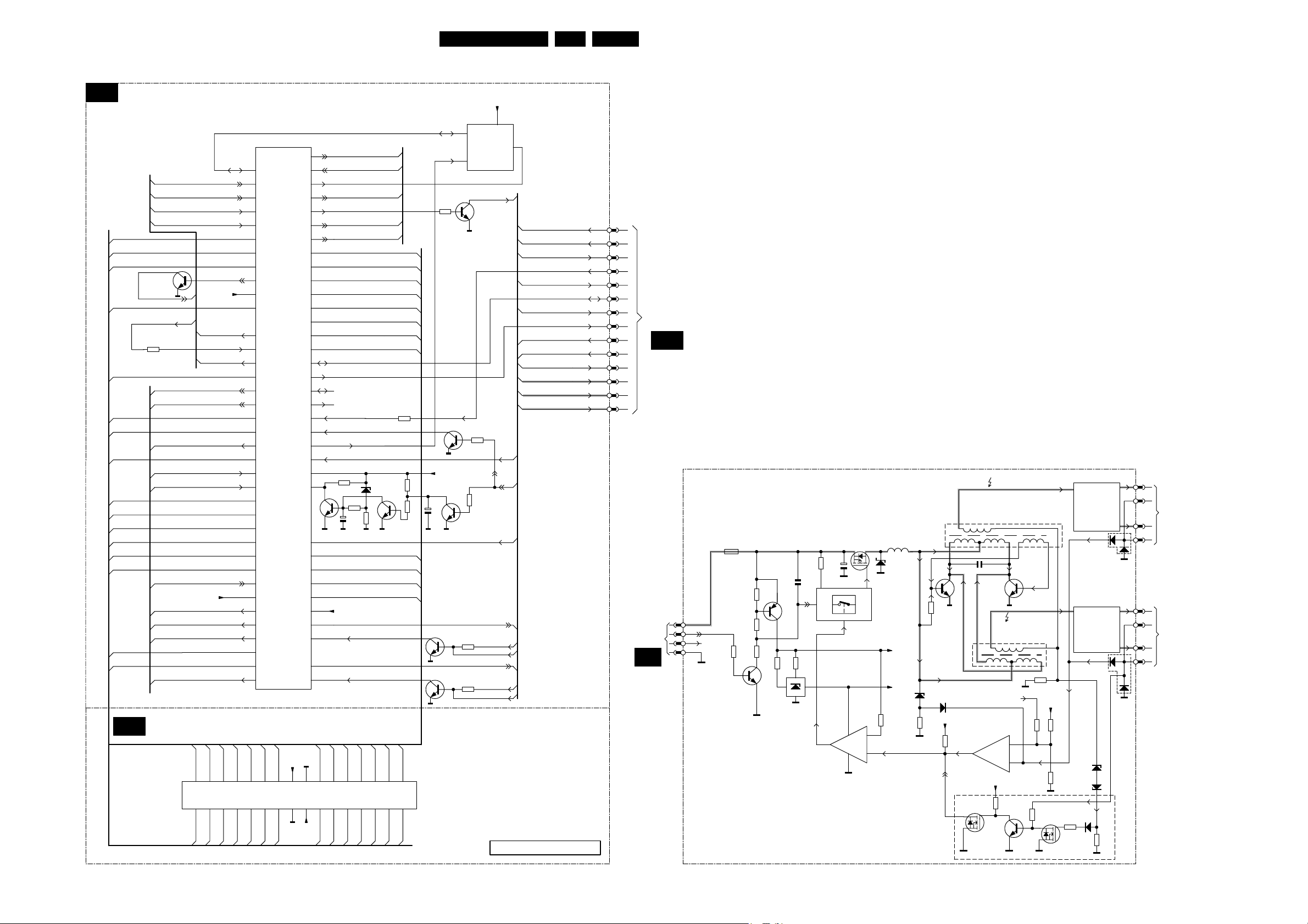
Block Diagrams, Testpoint Overviews, and Wiring Diagram
Block Diagram (TV Control and Inverter Panel)
CONTROLS
A 1
A11
A11
A(14)
OENOT
WENOT
STAND-BY
A(7)
PC-VSYNC
3037
A(6)
A(5)
A(4)
CENOT
A(15)
A(13)
A(12)
A(3)
A(2)
A(1)
A(0)
A(16)
MEMORY
A 2
(NOT FOR NTSC & LATAM)
FOR 100 PAGES
TELETEXT ONLY
(SCART)
STATUS2_SVHS-RR-DET
STATUS1 (SCART)
KEYBOARD
LIGHT-SENSOR_SDM
7062
A11
SYS1
A6
SYS2
A6
STBY-LED
A11
CVBS-TXT-CC
A6
G-SC1-IN_Y-IN
A11
SVHS-SIDE-DET
A11
+3V5
B-TXT-OSD
A4
G-TXT-OSD
A4
R-TXT-OSD
A4
FBL-TXT-OSD
A4
A(0)
1
A(16)
7064
IO1
100
+3V5
7070
+3V5
IO6
SDA-NVM
+3V5
TV-IRQ
COMM-LINE
A(2)
A(1)
2 3 4 5 6 7 8 9 10 11 12 13 14 15 16
A(15)
A(14)
A(3)
90
29
A(13)
NC
CENOT
OENOT
1
2
4
5
6
8
9
10
13
14
15
16
17
18
22
23
24
25
26
27
28
29
31
32
33
36
37
38
39
40
44
45
46
47
48
49
51
52
IO0
IO7
98
97
96
95
94
93
92
91
90
89
88
87
86
85
84
83
82
81
80
79
78
76
75
73
70
67
66
65
64
63
59
55
54
53
IO2
IO5
PC-TV-LED
HP-SIDE-DET
HIS-OFF
SEL-MAIN-FRNT-RR
SOUND-ENABLE
SDA-0
SCL-0
SCL-NVM
3081
7063
3082
2043
+3V5
IO3
A(4)
WENOT
2122232425262728303132
A(11)
A(12)
IO4
6031
3083
A(5)
A(10)
7069
A(6)
A(9)
3034
A(10)
A(11)
A(7)
17181920
A(8)
A11
A9
A5
A5
A9
IO7
IO6
IO5
IO4
IO3
IO0
A(8)
A(9)
IO2
IO1
30703071
3029
7068
+3V5
POWER-DOWN
7067
2057
SEL-IF-LL_M-TRAP
7053-B
7053-A
+3V5
7066
VCC
5
SDA
NVM
6
SCL
COMM-LINE
7022
3068
3072
CLOCK12MHZ
3055
VS-OSD
V-SYNC
SEL-MAIN-R1R2
3056
HS-OSD
H-SYNC
8
7
WC_
A11
A8
PC-HDAUDIO-L
PC-HDAUDIO-R
A8
STAND-BY
PC-HSYNC
PC-VSYNC
SDA-1
TV-IRQ
SCL-1
VS-OSD
HS-OSD
C-SYNC
A5
B-DRIVE
A4
G-DRIVE
A4
R-DRIVE
A4
RC5
A11
A10
A4
A5
A4
A5
A5
Version 1.2 Final 03-03-19
28LC03E 6.
1010
22
20
19
17
16
14
13
12
10
9
7
5
3
1
TO/FROM
1681 OF
SCALER BOARD
C 2
TO/FROM
1402 OF
SCALER
C 4
INVERTER (AMBIT)
ONLY FOR 15" & 17"
CN1
6,7,8
ON/OFF
5
4
Vbri
1,2,3
F1
R1 R5
CN2
R38
D30
1
3
TO LCD BACK-
LIGHT CONN.
CN3
1
3
CN4
1
3
TO LCD BACK-
LIGHT CONN.
CN5
1
3
CL 36532023_001.eps
160403
High AC voltage
BALANCE
CIRCUIT
T1
Q8
R8
C4,5
C3
R3
Q2
R4
R6
Q1
D1,Q3
Q4-Q6
R7
3
13
U1D
12
L1
D3,8
R19
+12V
+5V
D4
R10
11
+
10
-
R21
Q9
D5
+5V
R12
C10,11
14
Q51
High AC voltage
Vbri
+
U1C
-
+5V
Protection circuit
R60
Q10
9
8
Q53
R37
R62
BALANCE
R15
R17
R64
CIRCUIT
D31
D32,33
D6,7
D34
T2
+5V
Q14
Page 29
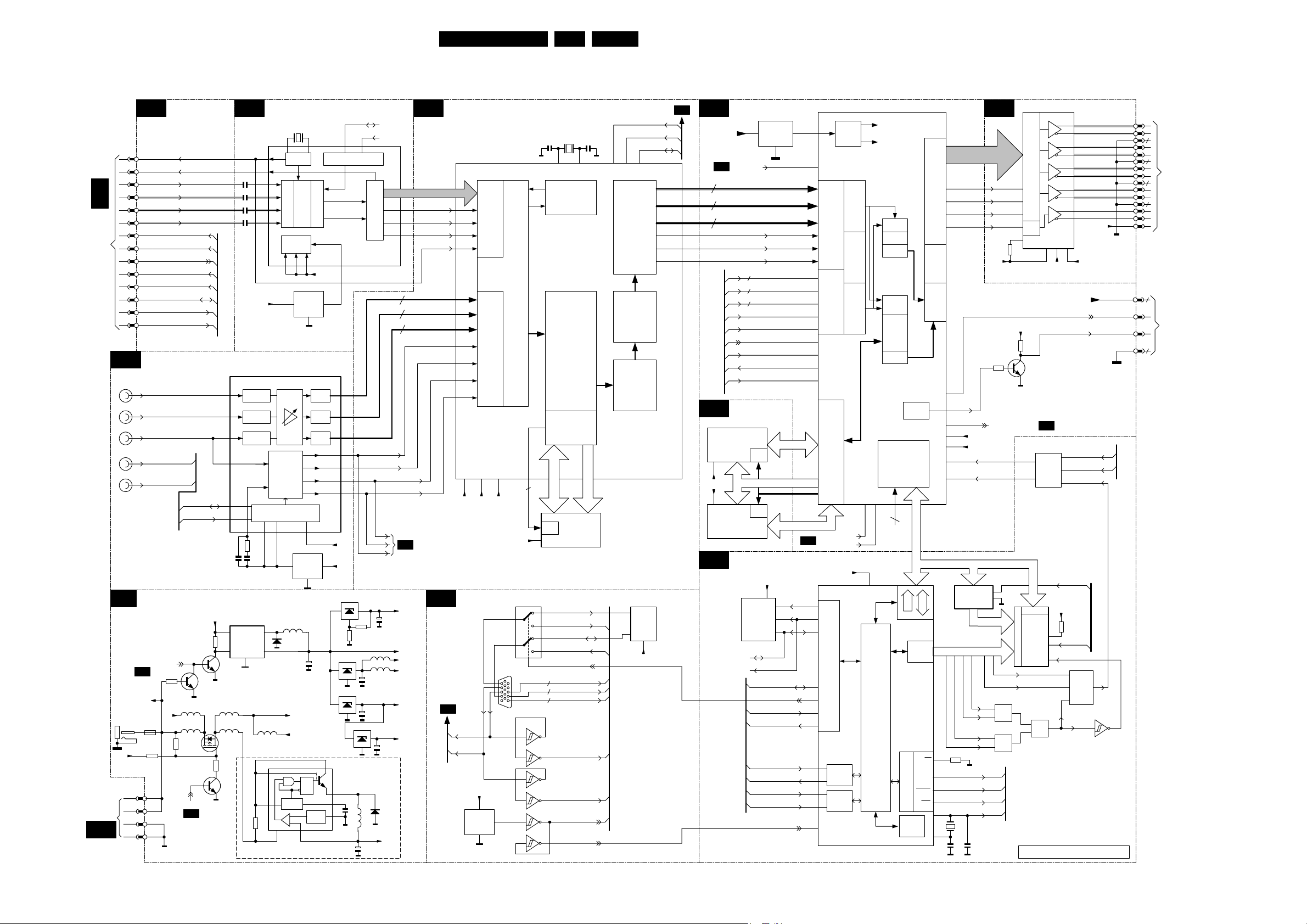
Block Diagrams, Testpoint Overviews, and Wiring Diagram
Block Diagram (Scaler Board)
29LC03E 6.
A 1
TO/FROM 1010 TV BOARD
12/24V
DC-IN
TO/FROM
1902 OF TV
BOARD
A 10
C 2
1681
10
9
7
5
3
1
22
20
19
17
16
14
13
12
HDTV - DECODER
C 10
HD I/P
Pr
Pb
Y
AUDIO
L
1001
PC-HDAUDIO-L
PC-HDAUDIO-R
R
POWER
C 1
POW-CON-SCALER
C2
12-24DC-SUP
1002
3014
+5V
1003
I/O & INTERFACE
VS-OSD
HS-OSD
AV-CVBS
(C-SYNC)
B-Pb
G-Y
R-Pr
PC-HDAUDIO-L
PC-HDAUDIO-R
POW-CON-SCALER
PC-HSYNC
PC-VSYNC
SDA-1
TV-IRQ
SCL-1
HDTV-V
HDTV-U
HDTV-Y
IICSDA
C8
IICSCL
C8
3001
5010
+5V
5011
(2)
3015
(1)
(1) = FOR 15"/17" ONLY
(2) = FOR 23" ONLY
4
PANEL-PWR-ON
3
2
C4
1
C10
C10
C1
C9
C9
C8
C8
C8
C2
C2
12-24DC-SUP
3005
7003
7002
(1)
5013
(2)
5015
7005
3016
7004
C 3
N10
C7
2304
K1
2305
F2
2308
G3
2315
D2
+5
7252
RAIN
54
Clamp A/D
BAIN
43
Clamp
GAIN
48
Clamp
SOGIN
49
SDA
57
56
SCL
VD
FILT
33
3264
2251 2253
7001
1
OUT
VIN
5
FB
ON|OFF
3
(1)
(2)
5014
8
7
3009/10
VIDEO DECODER
1301
7302
A3
Sync
AI12
AI32
AI22
Analog Input
AI42
Power
Ctrl
VXDD
VDDE
7301
3 2,4
IN
Sync
Proc
Clock
Gen
Serial Reg
PWR Mgmt
PVD
7251
OUT
5001
2
6002
4
(supply for LCD panel)
PAN-VCC
(2)
12V
7010
OSC
VCC
6
B4
Video Proc
VDDI
+3V3
OUT
ADJ
1
A/D
A/D
VDD
IN
ADJ
1
2007
Q
S
R
REF
5
P10 N9
IIC Reg Map
YCBCR
S
Decoder O/P
VDDA
SOGOUT
65
DATACLK
67
HSOUT
66
VSOUT
64
+3V3
32,4
+5
7008
32
3012
7007
3
7009
3
1
2
3
4
HDTV-SOG
HDTV-CLK
1
3011
2
2013
1
2
2015
1
7006
1
ONLY FOR 23"
2025
5025
2026
IICSDA
IICSCL
XPDO
:
XPD7
XRV
X-PORT
XRH
XCLK
HDTV-HSYNC
HDTV-VSYNC
2018
23
2006
6025
12V
C 9
DA-DATA 0....7
DA-FID
DA-HSYNC
DA-CLK
DA-VSYNC
8
V0..V7
8
U0..Y7
8
Y0..U7
C4
+2V5
+5
+2V5I
+2V5II
+3V3
+1V8
VIDEO CONVERTER
7351
206
208
195
207
5
4
1
2
VDD
+3V3
PC-IN
C 7
C2
PC-HSYNC
PC-VSYNC
7206
+5
3
VCC
RESET
GND
1
PORT
8 BIT
YCrCb
INPUT
PORT
24 BIT
YCrCb
INPUT
DAC_VDD
+3V3
2
INPUT PROC
AUTO SYNC
AUTO ADJ
1
VDDcore
+1V8
13
3
PC-IN
5
15
11
1
2
9
CLK & CONTROL
+3V3
7201
9
7203
1
34
5
98
11 10
13 12
191 192
CLK GEN
De-interlace
SDRAM
Interface
DATA 0...31
TIMING
SDRAM
REG
2M x 32
VDD/VDDQ
DDCSCL
12
RXD
15
1
DDCSDA
TXD
2
2
BLUEP&N
2
GREENP&N
REDP&N
2
2
PC-HSYNC-ASM
6
PC-VSYNC-ASM
1351
13M5
PLLs
NR
FRC
7352
23582356
RESET#
RESET
47
ADDR 0...10
C8
C8
C4
C4
C4
C4
C4
C4,C9
(NOT USED)
SOFT-RESET
IICSCL
IICSDA
46
45
O/P Proc
Sync Gen
DACs
Horizontal
and
Vertical
Enhancers
Horizontal
and
Vertical
Scalers
7202
6
DDC
NVM
5
DDC5V
OUTPUT (LVDS)
C 5
7501
27
28
30
31
PLL
32
PWRDWN
3511
+3V3
1,9,26
+5
3432
3434
7403
PANEL-PWR-ON C1
5
6
C1
EN
7754
DATA
FLASH
ROM
ADDR 0...17
MCA12
MCA13
7756-A
1
3
OR
2
9
10
7756-C
7756-B 7757-A
4
5
8
OR
C4, C8
C8
C8
C4
48
TXOUT0-
47
TXOUT0+
46
TXOUT1-
45
TXOUT1+
42
TXOUT2-
41
TXOUT2+
38
TXOUT3-
37
TXOUT3+
TTL PARALLEL-TO-LVDS
TXCLKOUT-
40
39
TXCLKOUT+
PAN-VCC
VCC
LVDSVCC
PLLVCC
34 44
+3LVDS
+3PLL
12-24DC-SUP
ON-OFF
Vbri
7755-A
1Y
1Y
MCWR#
2
1A
0
1
PSEN#
3
1A
1
JAGUAR#
1
2
1E
MCALE
+3V3
3758
31
WE
24
PSEN#
OE
22
PROMCS#
CE
7755-B
14
2A
0
13
2A12Y
1
15
2E
6
OR
12
Ver 1.1 Final 03-03-18
1506
2
4
10
12
18
20
6,7,8
26
28
34
36
40
1402
3
TO LCD PANEL
5
4
3
TO INVERTER PANEL
(15" & 17" ONLY)
1,2,3
C8
C8
11
3
SD31...63
WP-S
7402-JagASM
HDTV-HSYNC
C4
HDTV-VSYNC
7753
8
2
3
XIN
PARHS_PADE
FE
24-BIT
PORT
B
VGA
ADC
MCRESET#
MCALE
MCINT
MEMCLK
SDRAM
INTERFACE
P1.6
P1.0
P1.1
PLL1
PLL2
+5
VIDEO
CAPTURE
SMART SET
SURE SYNC
VIDEO
CAPTURE
PAHSYNC
VDD
MEM CLK
PANEL CLK
MUX
SCALER
MUX
SCALING
ENGINE
CONTROLLER
INTERFACE
PAVSYNC
44
SYNC
BE
MEM
BE
MICRO-
MCA8...9
PWM
ADR
ADR
<8:17>
MCAD0...7
DATA
TFT OUTPUT
OSD
OVERLAY
PIP
OVERLAY
PENBKL
PWM1
PENVDD
MCRD#
MCWR#
36...43
9, 19, 24...31
PRB, PRB, PBB
3 x 8-BIT TTL
FHSYNC
FVSYNC
FDE
FSHFCLK
+3V3
+2V5
JRD#
JWR#
MCAD0...7
7751
LATCH
MCA0...7
MCA8...17
C8
+3V3
1,4
1401
OSC GEN
SCALER
C 4
2
C4
HDTV-SOG
8
B-U-OUT 0...7
8
R-V-OUT 0...7
8
G-Y-OUT 0...7
C 6
HS-S23
VS-S23
CLK-S23
2
C7
C7
C7
C7
C7
C7
C8
C8
C8
REDP&N
2
GREENP&N
2
BLUEP&N
PC-HSYNC-ASM
PC-VSYNC-ASM
RESET#
MCALE
MCINT-ASM
MEMCLK
SDRAM
118
119
125
7471
+3V3
VDD/VDDQ
VDD/VDDQ
SDRAM
2M x 32
SDRAM
2M x 32
TIMING
REG
TSA0...10
CLK & CONTROL
TIMING
REG
SDO...31
7472
MICRO-P
C 8
+5
7752
8
7
6
NVM
5
8
IICSDA
IICSCL
C2
C2
C9
C7
C7
C2
C4
SDA-1
DCCCTL
SCL-1
SOFT-RESET
(NOT USED)
RXD
TXD
TV-IRQ
MCINT-ASM
4
P1.2
5
P1.3
7
P1.5
17
P3.5
11
UART
13
15
INT
14
10
RST
CPU
TIMING & CTRL
OSC
CLK
ALE
PSEN
WR
35
EA
33
32
18
20
21
MCA15
MCA14
3757
MCALE
PSEN#
MCWR#
MEMCLK
MCA16
1753
2753
MCA17
2754
CL 36532023_002.eps
190303
Page 30
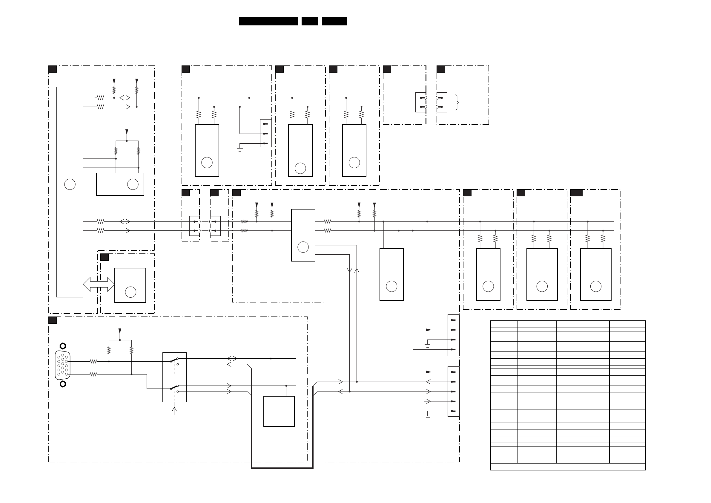
Block Diagrams, Testpoint Overviews, and Wiring Diagram
I2C-IC’s and Error Codes Overview
IIC
A1
+3V5
+3V5
A3
TUNER
A4
IF-VIDEO
30LC03E 6.
AUDIO
A8
PROCESSING
A6
COMB
FILTER
B
7064
SAA5667
U-CONT
ERR
12,29
82
81
1
78
84
83
3085
3017
SDA-NVM
SCL-NVM
7066
M24C32
(NVM)
EEPROM
3018
3019
A2
3048
3047
+3V5
3064 3065
56
ERR
10,11
SRAM
7070
CY7C1019CV33
SRAM
ERR
15
SDA-0
SCL-0
SDA-1
SCL-1
A1
1010
14
12
3100
3101
54
1100
TUNER
UR1316
ERR
13
C2
1681
14
12
COMPAIR
CONNECTOR
FOR SERVICE
(REACHABLE VIA
HOLE IN REAR
COVER)
uP
C8
+5
3753
3768
3754
1111
1426
5
6
3620
3332
3331
1
2
3
18
7301
TDA8845
17
BOCMA
VIDEO
PROC.
ERR
8
+5
3769
4
7
7753
PC251
uC
SCALER
ERR
29
3771
3
3770
2
11
13
3621
21
7620
MSP3410G
AUDIO
DECODER
ERR
14
+5
IIC SDA
IIC SCL
RXD
TXD
3751
+5
3752
56
M24C16
7752
NVM
ERR
25
1801
5
6
CONNECTION
FOR
3D COMB
FILTER
(OPTIONAL)
VIDEO
C3
DECODER
SAA7118E
DECODER
3327
P10 N9
7302
VIDEO
ERR
23
3328
VIDEO
C9
CONVERTER
FAROUJAS2300
CONVERTER
3356
46 45
7351
VIDEO
ERR
22
3354
HDTV
C10
DECODER
(only for AP, NAFTA
and LATAM)
AD9883AKST
3267
57 56
7252
HDTV
DECODER
ERR
24
3266
C7
PC-IN
6
1
5
10
1752
RXD
TXD
1751
1
2
3
4
1
2
3
4
5
FOR
DEBUGGING
PURPOSE
FOR
DEBUGGING
PURPOSE
IIC SDA
DDC5V
11
15
3216
12
3215
15
3212 3211
7201
74HC4052D
3
13
DDCCTL
1
DDCSDA
2
TXD
12
DDCSCL
15
RXD
7202
M24C02-WMN6
RXD
TXD
EEPROM
+3V3
IIC SCL
+5
RESET
Error codes
Error code Error description Possible defective
0 No error detected — ----
1 -3 Reserved
4 5V protection
5 Reserved
6 General I2C bus
7 Reser ved
8 BOCMA I2C error IC 7301 A4
9 BOCMA 8V supply
10 NVM I2C error IC 7066 A1
11 NVM identification
12 uProcessor internal
13 Tuner I2C error IC 1100 – UR13xx A3
14 Sound processor
15 SRAM I2C error IC 7070 A2
16 Reserved
17# 3D CF processor
18 - 20 Reserved
21 Scaler protection
22 Scaler protection
23 Scaler protection
24* HDTV decoder I2C
25 Scaler protection
26 Reserved
27 Scaler protection
28 Scaler protection
29 Scaler uP I2C error IC 7753 or IC 7064 C8, A1
* = Not app licable to Europe execution
# = Only for NAFTA 23” execution
active
error
failure
failure
RAM test failure
I2C error
I2C error
active
active
active
error
active
active
active
components
IC7930 or +5V I2C
devices
I2C bus s/c or o/c
IC 7910 or IC7301 A4, A10
IC 7066 A1
IC 7064 A1
IC 7620
(MSP34xx)
IC 7823 B
IC 7402 C4
IC 7351 C9
IC 7302 C3
IC 7252 C10
IC 7752 C8
IC 7471 C6
IC 7472 C6
Diagram
A3, A8, A10
A8
CL 36532023_039.eps
150403
Page 31

Block Diagrams, Testpoint Overviews, and Wiring Diagram
Powerlines Overview
31LC03E 6.
SUPPLY
UNIT
12V SS
24V LS
C1
1001-1 1
2
POW_CON_SCALER
12_24DC_SUP
C5
PAN_VCC
+3V3
POWER
5009
+5
5003
5004
+5
5012
+5
SS (12V) ONLY
5010
+5
LS (24V) ONLY
5011
SS (12V) ONLY
5013
LS (24V) ONLY
5015
OUTPUT (LVDS)
5521
5517
1002
7000mA
7001
5001
5002
21
CONTROL
7009
23
7006
23
7007
7008
7010
MC34063A
CONTROL
62
STABILIZER
23
23
+
5006
5005
7005
4
CONTROL
PANEL_PWR_CTR
5014
5025
5026
3517
3516
12_24DC_SUP
12_24DC_SUP
+5V
+3V3
+1V8
+2V5I
+2V5II
+2V5
PAN_VCC
+12V
+3V3
+3LVDS
+3PLL
1506
39
40
1003
+5V
+3V3
+1V8
+2V5I
+2V5II
+2V5
1
2
3
4
1x
5x
8x
1x
2x
1x
1x
LCD
MONITOR
MONITOR
CONNECTION
+3V3
VIDEO DECODER
C3
7301
+5
+3V3
C4
12_24DC_SUP
+3V3
+2V5
+25VI
+2V5II
+5V
C6
+3V3
C7
+2V5I
+3V3
+5V
1201
5
1
C8
+5
+3V3
C9
+3V3
+1V8
C10
+5
+3V3
5304
23
SCALER
5401
SDRAM (SCALER)
PC-IN
6212
10
PC INPUT
6211
15
3221
6
11
uP
VIDEO CONNECTOR
5354
5351
5352
5353
5357
HDTV-DECODER
(only for AP, NAFTA and LATAM)
7251
5258
23
5257
6261
(RESERVED)
K4-7302
+3V3
ON/OFF
+3V3
+3V3_ASM
+2V5
+25VI
+2V5II
+5V
+3V3
+2V5I
+3V3
+5V
3226
5206
+5
+3V3
+3V3
DAC_3V3
VDD_IO_3V3
+1V8
DAC_1V8
PLL_1V8
VDD_CORE_1V8
+5
(26-7252)
PVD
+5A
+3V3
+3V3
INVERTER (FOR 15" AND 17" ONLY)
IN
CN1
8
7
1402
6
7
8
5
DCC5V
1752
2
1751
1
+5
6
5
4
FOR
DEBUGGING
PURPOSE
ON/OFF
Vbri
F1
F4A
R1Q1R5
L2
L1
Q8
R8 C4,5
C3
R3
Q2
R4
R6
D1,Q3
Q4-Q6
CONTROL
Va
R7
5V
D3,8
BACK
LIGHT
OUTPUT
CN2
Vb
1
3
CN3
1
3
BACK
LIGHT
CN4
1
3
CN5
1
3
LOCAL SUPPLY
A10
1902
4
3
2
1
2
1
CONTROL
STANDBY
U_CONT
A1
+3V5
+5V4
MEMORY
A2
+3V5
TUNER
A3
+5V4
7120
CONVERTER
IF VIDEO
A4
+3V5
+5V4
+8V3
4303
VIDEO
A5
+5V4
+8V3
A6
+5V4
+8V3
12-24DC_SUP
AUDIO DELAY LINE
A7
+5V4
11V9
3
7900
DC/DC
5301
5601
12_24DC_SUP
1903
1600mA
5930
33u
+3V5
+5V4
+3V5
+5V4
9-1100
TUNING VOLTAGE
+3V5
+5V4
+8V3
+8V3A
+8V3A
+5V4
+8V3
+8V3A
+5V4
+8V3
+8V3
+5VD
3925
3904
3915
3930
5900
5901
1426
1
10
6925
TO 1801
3D COMP
(OPTIONAL)
N.C.
7920
CONTROL
AND
STABILIZER
7903,7904
POWER
DOWN
CIRCUIT
7910
CONTROL
AND
STABILIZER
7930
CONTROL
AND
STABILIZER
5921
26
POWER_DOWN
5911
27
5931
27
A8
+5V4
+8V3
AUDIO AMPLIFIER
A9
12_24DC_SUP_1
+3V5
SCART I/O
A11
12_24DC_SUP
+3V5
+8V3
FRONT LED
J
1170
2
7
250mA
300mA/400mA
320mA
+5V4
5620
+5V4A
+8V3
+12_24DC_SUP_1
+3V5
12_24DC_SUP
(FOR ITV ONLY)
+3V5
+8V3
+3V5
+8V3
CL 36532023_038.eps
12_24DC_SUP
12_24DC_SUP-1
+3V5+3V5
+8V3+8V3
+5V4+5V4
+3V5
+8V3
100403
1231
2x
1x
5x
5x
7x
2
7
Page 32

Block Diagrams, Testpoint Overviews, and Wiring Diagram
Testpoint Overview TV Board (15”/17”)
32LC03E 6.
3139 123 5592.4
CL 36532023_035.eps
061003
Page 33

Block Diagrams, Testpoint Overviews, and Wiring Diagram
33LC03E 6.
Mapping Testpoint Overview and Waveforms TV Board (15”/17”)
F002 B4
F003 C5
F004 C5
F006 C4
F007 C4
F008 B5
F010 C4
F011 B4
F012 C4
F013 C4
F014 C5
F015 C5
F022 C4
F025 C5
F032 C5
F044 C4
F045 B4
F046 B4
F054 C4
F066 B5
F068 C4
F070 A5
F071 A5
F072 A5
F073 A5
F074 A5
F075 A5
F076 A4
F077 A5
F080 B4
F085 A4
F101 B8
F102 B7
F103 B6
F104 B6
F105 A8
F106 C7
F107 C8
F108 C7
F109 B8
F201 B8
F202 C8
F203 C8
F204 C8
F205 C8
F206 C8
F207 C8
F208 D8
F209 D8
F210 D8
F211 D7
F212 D7
F213 D6
F214 D6
F215 D6
F216 D6
F217 D6
F218 D8
F219 D5
F221 D6
F222 D5
F223 D5
F224 D6
F225 D4
F226 D4
F227 D5
F228 D5
F229 D5
F230 D6
F231 D5
F232 D7
F233 D7
F234 D7
F235 D7
F236 D7
F237 D7
F238 D7
F301 B5
F302 A6
F321 A5
F337 B5
F338 A5
F339 B5
F340 B5
F341 B5
F342 B5
F345 A5
F346 B5
F349 B5
F350 B5
F351 A5
F352 A5
F355 A5
F358 A5
F385 A6
F413 B5
F426 C6
F427 C6
F428 C6
F429 C6
F430 C6
F431 C6
F432 B6
F470 B4
F471 B5
F472 B5
F473 B4
F474 B4
F476 A4
F477 A5
F478 A5
F479 B5
F480 B5
F601 B1
F602 B1
F603 B1
F610 B1
F612 C1
F613 D1
F620 B3
F621 B3
F622 B4
F626 B3
F640 B3
F645 A3
F646 A3
F650 B2
F655 C3
F656 B3
F676 B3
F731 B1
F732 C2
F735 C2
F736 D2
F737 D2
F738 D3
F739 C2
F740 C2
F743 C4
F745 C1
F755 C3
F759 D3
F900 A1
F901 A2
F902 A1
F903 C3
F906 A1
F907 A3
F908 A4
F044
1V / div DC
5ms / div
F054
1V / div DC
20µs / div
F080 = 2V3 DC
F107
1V / div AC
20µs / div
F108
1V / div DC
20µs / div
F340
1V / div DC
20µs / div
F341
1V / div DC
20µs / div
F342
1V / div DC
20µs / div
F346
1V / div DC
20µs / div
F350
1V / div DC
20µs / div
F352
200mV / div DC
20µs / div
F358
200mV / div DC
20µs / div
F385
200mV / div DC
20µs / div
F413
1V / div DC
20µs / div
F426
200mV / div DC
20µs / div
F428
2V / div DC
20µs / div
F470
500mV / div DC
20µs / div
F471
500mV / div DC
20µs / div
F472
500mV / div DC
20µs / div
F480
1V / div DC
20µs / div
F602
2V / div AC
2ms / div
F603
2V / div AC
2ms / div
F622
100mV / div AC
5µs / div
F735
20mV / div AC
1ms / div
F736
20mV / div AC
1ms / div
F740
20mV / div AC
1ms / div
F906 = 8V3 DC
F907 = 5V4 DC
F908 = 3V5 DC
CL 36532023_092.eps
110903
Mapping Testpoint Overview and Waveforms Scaler Board
F001 A7
F002 A7
F003 D1
F005 B1
F006 D1
F007 D1
F008 A7
F026 C1
F201 B7
F202 A7
F203 A7
F204 A7
F205 A7
F206 B7
F207 B7
F210 A7
F218 A7
F222 A7
F250 B7
F251 C7
F252 D7
F253 C7
F254 B7
F256 C7
F351 C5
F352 C5
F353 C5
F354 C6
F355 C6
F356 C6
F401 A3
F402 A3
F403 A3
F404 A3
F405 B6
F528 A3
F529 B3
F530 B3
F531 B3
F532 B3
F533 B3
F534 B3
F535 A3
F536 A3
F537 B6
F538 A4
F539 B4
F540 A3
F541 B3
F542 A3
F681 D1
F682 D1
F683 D1
F684 D2
F685 D1
F686 D2
F687 D2
F688 D2
F689 D2
F690 D2
F691 D2
F692 D2
F693 D2
F694 D2
F751 C2
F752 C2
F753 C2
F754 B2
F755 C2
F756 C2
I001 A2
I002 A1
I003 A1
I004 B1
I005 A2
I006 A2
I007 A2
I008 A2
I009 C1
I009 D1
I010 A6
I011 A6
I012 A6
I013 D5
I013 D6
I014 A3
I015 A6
I016 A6
I017 B1
I018 A1
I018 B1
I019 A6
I200 A7
I201 B6
I202 B7
I203 C6
I204 A6
I205 A7
I206 C6
I207 B7
I208 A6
I209 C7
I210 C7
I231 C6
I232 D7
I233 C6
I234 D7
I235 C7
I236 D5
I237 C6
I238 D7
I239 C6
I240 C6
I241 D6
I242 D6
I244 D6
I246 D6
I247 D6
I248 D7
I249 C7
I250 D6
I251 C6
I252 D7
I254 C6
I255 D6
I256 D6
I258 D6
I259 D6
I260 C6
I261 D6
I262 D6
I263 C7
I264 D6
I265 D6
I266 C7
I267 D6
I268 D6
I269 D6
I270 D6
I271 D6
I272 D4
I273 D6
I274 D6
I275 D6
I276 D6
I278 D6
I279 C7
I280 D6
I281 D6
I282 D4
I283 D6
I284 D4
I285 D6
I286 D6
I288 D6
I289 D6
I290 D4
I291 C6
I291 D6
I292 D4
I293 C6
I294 C6
I294 D6
I295 C6
I296 D5
I297 C6
I298 D5
I301 C2
I302 C2
I303 D2
I304 D3
I305 C2
I306 D1
I316 C2
I321 C2
I322 C2
I323 C2
I324 C2
I325 C2
I326 C2
I327 C2
I345 D2
I346 D2
I347 C2
I348 C2
I348 D2
I349 D2
I351 D3
I353 D3
I354 C3
I356 D3
I358 D3
I360 D3
I362 D3
I363 D3
I364 D3
I365 D4
I366 D4
I367 D3
I368 D3
I370 D3
I371 D2
I372 D4
I373 D3
I374 D3
I375 D3
I376 C5
I377 C3
I378 C4
I379 C4
I381 C4
I382 B4
I384 C4
I385 C4
I386 C5
I387 C4
I388 C5
I390 C5
I391 C5
I392 C5
I393 C5
I394 C5
I401 B6
I402 C6
I403 B4
I404 C6
I405 A5
I406 A5
I407 A4
I408 A4
I409 A5
I410 A5
I411 A4
I412 A5
I413 A5
I414 A5
I415 A4
I416 A5
I417 A5
I418 A4
I419 A5
I420 A6
I421 A6
I422 B6
I423 A4
I424 A3
I425 A4
I426 B5
I427 B6
I428 B6
I429 A6
I430 B6
I431 A4
I432 A5
I433 A6
I434 A6
I435 A6
I436 B5
I437 A4
I438 A4
I439 A4
I440 A5
I441 A4
I442 A4
I443 A4
I444 A5
I445 A5
I446 A5
I447 A5
I448 B5
I450 B6
I451 B6
I452 B5
I452 B6
I455 B6
I456 A5
I457 A6
I458 A6
I460 B4
I461 A5
I462 B5
I463 B4
I464 B4
I469 B4
I470 A5
I471 A4
I472 A6
I473 A4
I474 A4
I475 A6
I506 B4
I507 B4
I508 B4
I509 B4
I510 B4
I511 B4
I512 B4
I513 B4
I514 B4
I515 B4
I516 B4
I517 B4
I518 A4
I519 B4
I520 B4
I521 B4
I522 B4
I523 A4
I524 A4
I525 A4
I526 A4
I527 B4
I601 A4
I601 A5
I602 A5
I603 A5
I604 B6
I605 A4
I606 A4
I607 B5
I608 A5
I609 A5
I610 A5
I611 A6
I612 A6
I613 A4
I614 B5
I615 A5
I616 B4
I617 A5
I618 A5
I619 A4
I620 A4
I621 A5
I751 B1
I751 B2
I752 B2
I753 B2
I754 B1
I755 B2
I756 A2
I756 B2
I757 B2
I758 C2
I762 A1
I763 B3
I766 B2
I767 A2
I768 A2
I769 A2
I770 A2
I771 C2
I772 B2
I773 A2
I774 A2
I775 B2
I776 B2
I776 B3
I777 A2
I778 A2
I779 A2
I781 A3
I781 B3
I782 A2
I783 B1
I784 A2
I785 A1
I786 B2
I787 A2
I788 A1
I789 A1
I790 A2
I790 B2
I792 A2
I793 A2
I794 A1
I795 A1
I795 B1
I796 A1
I797 A1
I798 A1
I799 B3
F008 = 5V DC
F026 = 12V DC
F351
1V / div DC
10µs / div
F352C
1V / div DC
5ms / div
F353
500mV / div DC
5µs / div
F354
500mV / div DC
10µs / div
F355
200mV / div DC
20µs / div
F355C
500mV / div DC
5µs / div
F402 = 3V2 DC
F403 = 4V6 DC
F405
1V / div DC
20ns / div
F529
500mV / div DC
10µs / div
F530
500mV / div DC
10µs / div
F531
500mV / div DC
10µs / div
F532
500mV / div DC
10µs / div
F533
500mV / div DC
10µs / div
F534
500mV / div DC
10µs / div
F535
500mV / div DC
10µs / div
F536
500mV / div DC
10µs / div
F537 = 3V3 DC
F538 = 3V2 DC
F539 = 3V DC
F541
500mV / div DC
10µs / div
F542
500mV / div DC
10µs / div
F689
1V / div DC
5ms / div
F690
1V / div DC
20µs / div
F691
200mV / div DC
20µs / div
F692
200mV / div DC
10µs / div
F693
200mV / div DC
10µs / div
F694
200mV / div DC
10µs / div
F755
1V / div DC
50µs / div
F756
1V / div DC
50µs / div
I009 = 3V3 DC
I012 = 2V5 DC
I013 = 1V8 DC
I016 = 2V5 DC
I304 = 3V3 DC
I327
1V / div DC
2µs / div
I472 = 3V3 DC
I473 = 3V3 DC
I474 = 3V3 DC
I475 = 3V3 DC
CL 36532023_093.eps
150403
Page 34

Block Diagrams, Testpoint Overviews, and Wiring Diagram
Testpoint Overview Scaler Board
34LC03E 6.
3139 123 5680.3
CL 36532023_036.eps
061003
Page 35

Block Diagrams, Testpoint Overviews, and Wiring Diagram
Testpoint Overview TV Board (23”)
F002 B4
F003 C5
F004 C5
F006 C4
F007 C4
F008 B5
F010 C4
F011 B4
F012 C4
F013 C4
F014 C5
F015 C5
F022 C4
F025 C5
F032 C5
F044 C4
F045 B4
F046 B4
F054 C4
F066 B5
F068 C4
F070 A5
F071 A5
F072 A5
F073 A5
F074 A5
F075 A5
F076 A4
F077 A5
F080 B4
F085 A4
F101 B8
F102 B7
F103 B6
F104 B6
F105 A8
F106 C7
F107 C7
F108 C7
F109 B8
F201 B8
F202 C8
F203 C8
F204 C8
F205 C8
F206 C8
F207 C8
F208 C8
F209 D8
F210 D8
F211 D7
F212 D7
F213 D6
F214 D6
F215 D6
F216 D6
F217 D6
F218 D8
F219 D5
F221 D6
F222 D5
F223 D5
F224 D6
F225 D4
F226 D4
F227 D5
F228 D5
F229 D5
F230 D6
F231 D5
35LC03E 6.
F232 D7
F233 D7
F234 D7
F235 D7
F236 D7
F237 D7
F238 D7
F301 B5
F302 A6
F321 A5
F337 B5
F338 A5
F339 B5
F340 B5
F341 B5
F342 B5
F345 A5
F346 B5
F349 B5
F350 B5
F351 A5
F352 A5
F355 A5
F358 A5
F385 A6
F413 B5
F426 C6
F427 C6
F428 C6
F429 C6
F430 C6
F431 C6
F432 B6
F470 B4
F471 B5
F472 B5
F473 B4
F474 B4
F476 A4
F477 A5
F478 A5
F479 B5
F480 B5
F601 B1
F602 B1
F603 B1
F610 B1
F612 C1
F613 D1
F620 B3
F621 B3
F622 B4
F626 B3
F640 B3
F645 A3
F646 A3
F650 B2
F655 C3
F656 B3
F676 B3
F731 B1
F732 C2
F735 C2
F736 D2
F737 D2
F738 D3
F739 C2
F740 C2
F743 C4
F745 C1
F755 C3
F759 D3
F900 A1
F901 A2
F902 A1
F903 C3
F906 A1
F907 A3
F908 A4
3139 123 5682.2
CL 36532054_003.eps
061003
Page 36

Block Diagrams, Testpoint Overviews, and Wiring Diagram
Wiring Diagram (15”/17”)
Wiring Diagram 15" & 17"WS
36LC03E 6.
Top Control Panel
E
1500_4P
Right
Speaker
TO
D
BACK
LIGHTS
Side I/O Panel
LCD PANEL
IN
Inverter
Panel
CN3_2P CN2_2P
CN1_8P
C
1402_8P
TO LCD PANEL
Scaler Board
1003_4P
1681_22P
TV Board
A
Left
Speaker
1902_4P
1732_4P
J
Front LED
Panel
1170_7P
TO
BACK
LIGHTS
0240_11P
CN4_2P CN5_2P
1506_40P
1010_22P
1111_3P
ComPair
1234_4P
1231_7P
3225_11P
CL 36532023_060.eps
080403
Page 37

Block Diagrams, Testpoint Overviews, and Wiring Diagram
Wiring Diagram23 Inch Wide Screen
37LC03E 6.
Wiring Diagram 23"WS
Top Control Panel
E
LCD PANEL
Scaler Board
C
1500_4P
TO LCD PANEL
A
TV Board
D
Side I/O Panel
0240_11P
Right Speaker
Front LED
J
Panel
1170_7P
LIGHTS
TO BACK
1402_8P
1506_40P
1003_4P
1681_22P
1902_4P
1010_22P
1732_4P
1111_3P
ComPair
1734_3P
Left Speaker
1234_4P
1231_7P
3225_11P
CL 36532054_024.eps
010903
Page 38

Circuit Diagrams and PWB Layouts
7. Circuit Diagrams and PWB Layouts
TV Board: U_Cont
U_CONT
38LC03E 7.
A
B
C
D
E
F
(COMMON)
1 2 3 4 5 6 7 8 9
3022
2K2
PC-HSYNC
A1
KEYBOARD
A11
LIGHT-SENSOR_SDM
A11
OENOT
A2
WENOT
A2
TV-IRQ
A1
STATUS2_SVHS-RR-DET
A11
HIS-OFF
A5
SOUND-ENABLE
A9
A9,A10
HP-SIDE-DET
A9
POWER-DOWN-INT
A1
POWER-DOWN
A10
COMM-LINE
A11
(SCART)
1010
TO 1681 OF SCALER S23 CL BOARD
PC-HDAUDIO-L
22
0V
21
PC-HDAUDIO-R
20
0V
19
STAND-BY
2V9
18
PC-HSYNC
17
0V
PC-VSYNC
16
0V
15
14
4V8
13
5V
12
4V8
11
10
0V
9
0V5
8
7
0V6
6
5
0V6
4
3
0V6
2
1
0V6
SDA-1
TV-IRQ
SCL-1
VS-OSD
HS-OSD
C-SYNC
B-DRIVE
G-DRIVE
R-DRIVE
STAND-BY
A8
A8
F070
F071
A1
F077
F073
A1
F074
A1
F072
A1
A5
A4
A4
A4
3034
A4
A5
100R3021
F080
V-SYNC
H-SYNC
10K
3068
+3V5
3037
10K
3038
3072
100K
47K
10K
0V6
BC847BW
4008
RES
7008
BFS20
3006
10K
2V9
0V6
7068
BC847BW
4036
RES
0V
BC847BW
7067
3053
10K
3052
10K
7036
0V
3008
10K
+3V5
3036
10K
FOR DIVERSITY TABLE SEE DIAGRAM A2
+3V5
SDA-NVM
3063
2K2
2057
4u7
+3V5
7062
+5V4
0V
3V5
0V
F075
5
SDA
3V5
BC847BW
0V
3014
8K2
+3V5
3069
15K
3070
27K
3071
100K
7069
BC847BW
3V3
F076
VSS
4
+3V5
3V5
8
+5V4
VCC
7066
M24C32
NVM
+3V5
3015
10K
3046
4K7
BZX284-C2V4
F068
3083
470R
7022
BC847BW
3062
47K
6031
3082
10K
+3V5
0V
E0
E1
E2
SCL
WC_
3023
8K2
1SS355
1
3V5
3V5
STBY
+3V5
0V7
3029
10K
6020
2
3
SCL-NVM
6
7
WC-NVM
F066
SERVICE
F085
3081
4K7
7063
BC847BW
2043
4u7
P50-COMM
NOT FOR
+3V5
2049
220n
+3V5
3099
FOR
3094
10K
NTSC &
LATAM
0V
2053
10u
F045
3045
12K
+3V5
2012
RES
3032
10K
3028
47K
+3V5
+3V5
3065
4K7
3084
100R
2045
18p
2010
820p
IO(0)
F003
F002
3055
10K
+3V5
3056
47K
4K7
3064
3V5
3V5
NC
A(14)
3V5
3V5
5V1
NC
0V5
0V
2V7
3V5
5V3
0V2
F046
7064
5
7
8
10
11
12
13
0V
14
18
17
19
2
95
96
97
99
93
85
98
BC847BS
2018 2n2
3086 100R
3V5
(1)
P3.2/ADC2
P3.3/ADC3
A15_LN
A14
_RD
_WR
VSSC
7053-B
3060
10K
18p
2019
RES
2046
F004
NC
3
1
A17_LN
P2.7/PWM6
VSSP
P0.5
_EA
P0.2/INT2
P0.1/TX
_PSEN
P3.0/ADC0
P2.3/PWM2
P2.4/PWM3
P2.5/PWM4
VSSC
P2.1/PWM0
AD0
P2.6/PWM5
3057
RES
+5V4
3013
3024
8K2
1K
3042
150R
F008
IO(2)
NC
0V
3V5
A(12)
47 48
37 38
G
AD2
A12
MOVX_WR
P3
0 - 7
P0
0 - 7
P2
0 - 7
RESET
_RESET
0V
F007
+3V5
3044
10K
2055
RES
0V2
P1.1/T0
MOVX_RD
NC
+3V5
3V5
P2.2/PWM1
I2C-bus,
general I/O
ROMBK.0
ROMBK.1
7053-A
BC847BS
P0.0/RX
F006
3V5
2052
RES
0V
5V3
94
4
P3.1/ADC1
ROM
(128 K/
192 K
BYTES)
ROMBK.2
F044
F054
3054
10K
3003
10K
F022
+5V4
RES
3012
A(7)
8K2
3009
A(8)
1516
6768
A7
A8
DISPLAY
VSYNC
3V5
+5V4
IO(1)
IO(7)
8687 88899909192
AD1
AD7
DATA
CAPTURE
RAMBK.0
5152535455565758 59660616263646566
A(16)
2056
RES
+3V5
75 767778 79
VDDP
A9
A10
A(10)
A(9)
+3V5
5041
4u7
A11
A(11)
+3V5
0V
0V
A(3)
3V5
80 81828384
100
R
A3
P1.3/TI
P2.0/TPWM
TV CONTROL
AND
INTERFACE
MICRO-
PROCESSOR
MEMORY
INTERFACE
P3.5/INT5
HSYNC
VDS
4V8
3V5
0V1
3061
470R
3058
470R
3030
1K
+3V5
5042
4u7
100n2044
NC
3V5
3V5
P1.1/T0
A16_LN
P1.0/INT1
VDDC
VSSC
3V5
F010
3004
8K2
2051
100n
3066
8K2
100p
2050
IO(6)
2V6
AD6
IO
A0 - A16
DRAM
(14 KBYTES)
VSSP
P3.6
_INTD
NC
0V
+5V4
IO(5)
AD5
F025
IO(4)
AD4
3059
150R
IO(3)
AD3
P0.6
28
3V5
2020
RES
F011
3V
4V8
2V8
4V8
P1.4/SCL1
P1.6/SCL0
P1.7/SDA0
P1.5/SDA1
P3.4/PWM7/T2EX
P1
0 - 7
SYNC_FILTER
XTALIN
XTALOUT
OSCGND
70717273 74
69
+3V5
3010
2K2
3088
3050
3018 100R
*
3019
*
3017 100R
(1)
EU & AP-PAL
NTSC-AP
NTSC & LATAM
46
B
45
VDDC
44
43
_COR
42
VPE
41
FRAME
40
A1
39
A2
RAMBK.1
50
NC
49
A0
A(13)
36
A13
35
IREF
34
A(15)
33
A15_BK
32
CVBS1
31
CVBS0
30
VSSA
29
P0.7/T2
27
A4
26
A5
25
P3.7
24
P0.4/INT4
23
A6
22
P0.3/INT3
21
VPE
20
ALE
NC
1057
RES
2042
RES
0V
3V5
3V5
A(1)
A(2)
A(0)
1V3
0V7
A(4)
A(5)
A(6)
100R
100R
100R
100R3085
NC
F012
NC
0V
1V
5V
0V
2041
RES
POWER-DOWN-INT
SDA-1
SCL-1
SAA5667
SAA5645
SAA5647
F015
F014
F013
P50-INT
F032
A1
A1
A1
5040 4u7
2017
3016 1K0
3051 24K
+3V5
F044
1V / div DC
5ms / div
+3V5
+3V5
100n
100n2016
1u02015
1u02014
3035
470R
3049
10K
3007 8K2
4057
3048
+3V5
F054
1V / div DC
+3V5
20µs / div
SEL-MAIN-FRNT-RR
3047
2K22K2
RESRES
20472048
3043
150R
3033
10K
2054
3092 100R
3031
2013
3093
RES
+5V4
8K23002
CLOCK12MHZ
SEL-IF-LL_M-TRAP
FBL-TXT-OSD
SEL-MAIN-R1R2
G-TXT-OSD
(SCART)
STATUS1
PC-TV-LED
R-TXT-OSD
RC5
IO(0:7)
A3,A4,A6,A8
SDA-0
SCL-0
A3,A4,A6,A8
B-TXT-OSD
RES
2021
SVHS-SIDE-DET
A(0:16)
G-SC1-IN_Y-IN
RES
CVBS-TXT-CC
470R
RES
1%
CENOT
SYS2
SYS1
F080 = 2V3 DC
STBY-LED
CL 36532023_004.eps
150403
A5,A8
A4
A5
A11
A11
A4
A11
A2
A4
A11
A2
A11
A6
A2
A6
A6
A4
A11
A5
A4
A
B
C
D
E
F
1010 C1
1057 E7
2010 B4
2012 E3
2013 D9
2014 D8
2015 C8
2016 C8
2017 C8
2018 F4
2019 A4
2020 A7
2021 C9
2041 F8
2042 F7
2043 E3
2044 A6
2045 B4
2046 A4
2047 B9
2048 B9
2049 A3
2050 A6
2051 F6
2052 F5
2053 A3
2054 C9
2055 F5
2056 F6
2057 E2
3002 E8
3003 F5
3004 F6
3006 A2
3007 E9
3008 A2
3009 A5
3010 F7
3012 A5
3013 A5
3014 C2
3015 C2
3016 C8
3017 B7
3018 B7
3019 B7
3021 A1
3022 A1
3023 D3
3024 A5
3028 F4
3029 F3
3030 F5
3031 D9
3032 F4
3033 C9
3034 A1
3035 D9
3036 D2
3037 D2
3038 E2
3042 A5
3043 C9
3044 E5
3045 B3
3046 D3
3047 B9
3048 B9
3049 D8
3050 A7
3051 C8
3052 F2
3053 F2
3054 F5
3055 F4
3056 F4
3057 F4
3058 F6
3059 A7
3060 F4
3061 F6
3062 C3
3063 B2
3064 A4
3065 A4
3066 A6
3068 D1
3069 D2
3070 E2
3071 E2
3072 E1
3081 E3
3082 E3
3083 E3
3084 A4
3085 B7
3086 A4
3088 A7
3092 C9
3093 D9
3094 D3
3099 C3
4008 A2
4036 E2
4057 E9
5040 C8
5041 F6
5042 A6
6020 F3
6031 E3
7008 A2
7022 F3
7036 E2
7053-A F5
7053-B E4
7062 C2
7063 E3
7064 B4
7066 A3
7067 F2
7068 D2
7069 E2
F002 D4
F003 D4
F004 B5
F006 E5
F007 E5
F008 B5
F010 E6
F011 A7
F012 C8
F013 D8
F014 D8
F015 D8
F022 F5
F025 E7
F032 E8
F044 E5
F045 A3
F046 A4
F054 E5
F066 B3
F068 E3
F070 D1
F071 D1
F072 E1
F073 E1
F074 E1
F075 F2
F076 F2
F077 E1
F080 C1
F085 D3
1 2 3 4 5 6 7 8 9
Page 39

Circuit Diagrams and PWB Layouts
(
(
(
(
(
TV Board: Memory for 100-pg Teletext
1 2
39LC03E 7.
Personal Notes:
A
B
C
MEMORY FOR 100-PG TELETEXT
(COMMON FOR EUROPE & AP-PAL)
A(0)
A(1)
A(2)
A(3)
A(4)
A(5)
A(6)
A(7)
A(8)
A(9)
A(10)
A(11)
A(12)
A(13)
A(14)
A(15)
A(16)
A1
A1
A1
OENOT
WENOT
CENOT
DIVERSITY TABLE DIAGRAM A1 AND A2
3V3
3V3
3V3
3V3
3V3
0V
3V5
0V
0V
3V5
3V4
0V
0V
0V
0V
0V
0V
3V3
3V3
3V3
1
2
3
4
13
14
15
16
17
18
19
20
21
29
30
31
32
28
12
5
2060
100n
0
1
2
3
4
5
6
7
8
9
10
11
12
13
14
15
16
OE
WE
CE
+3V5
5050
4u7
3V5
8
24
VCC
RAM
128Kx8
0
A
128K-1
VSS
9
25
0
DQ
7
2061
100n
7070
CY7C1019CV33
6
7
10
11
22
23
26
27
3V3
0V
0V
0V
0V
0V
0V
0V
2060 A1
2061 A2
5050 A2
7070 A2
A
B
IO(0)
IO(1)
IO(2)
IO(3)
IO(4)
IO(5)
IO(6)
IO(7)
C
NAFTA
AP -/69
V
Latam
AP-NTSC -/61
V
V
Component type
COL) R
COL) R
PHSE) Y
PHSE) Y
PHSE) Y
Europe -/58
Europe -/12
Item#
VV V
2060 -- -- -- CER2 0603 X7R 16V 100N COL
VV V
2061 -- -- -- CER2 0603 X7R 16V 100N COL
VV V
3028 -- -- -- RST SM 0603 47K PM5 COL
VV V
3029 -- -- -- RST SM 0603 10K PM5 COL
VV V
3032 -- -- -- RST SM 0603 10K PM5 COL
VV V
3049 -- -- -- RST SM 0603 10K PM5 COL
VV V
3094 -- -- -- RST SM 0603 10K PM5 COL
VV V
5050 -- -- -- FXDIND SM 0805 4U7 PM10 COL R
VV V
6020 -- -- -- DIO SIG SM BAS316
VV V
7022 -- -- -- TRA SIG SM BC847BW
VV V
7064 -- -- -- IC SM SAA5667HL/M1/
7064 -- -- -- -- -- IC SM SAA5645HL/M1
7064 -- -- -- -- IC SM SAA5647HL/M1
7070 -- -- -- IC SM CY7C1019CV33-15ZC(CYPR)R
VV
V
1 2
CL 36532023_005.eps
150403
Page 40

Circuit Diagrams and PWB Layouts
TV Board: Tuner Function
TUNER FUNCTION
(15"/17"/23" SCART)
40LC03E 7.
A
B
C
D
E
1 2 3 4 5 6 7 8 9
AP -/61 & Latam
Item#
1100 -- -- TUNER UR1316/A I H-3
1100 -- -- TUNER UR1336/A F S H-3
2108 -- -- -- ELCAP 6V3 S 470U PM20 COL A
2108 -- ELCAP 25V S 100U PM20 COL A
2109 -- -- FIL CER 39MHZ75 MKTGA* BS A
3102 -- -- RST SM 0603 10K PM5 COL
3102 -- -- RST SM 0603 JUMP. 0R05 COL
3103 -- -- RST SM 0603 1K5 PM5 COL
3103 -- -- RST SM 0603 2K2 PM5 COL
3136 -- -- RST SM 0603 100R PM5 COL
6102 -- -- DIO SIG SM BAS316 (COL) R
Europe -/12 & -/58
VV
V
VV
VV
VV
COMPAIR
1111
A1
A1
A8
NAFTA
VV
VV
VV
VV
VV
VV
1
2
3
AP -/69
V
SCL-0
SDA-0
SIF-FM
Component type
3130
1K2
2V7
7130
BFS20
1V8
3131
270R
F105
F107
F108
2V5
PAL / SECAM
NTSC / LATAM
1100
*
12
13
MT
14
15
AS SCL SDA +5V ADC
3100
0R
3101
0R
3132
100K
2130
1n0
7131
BFS20
1n0
(PENDING FOR 12NC)
# LOCALLIB
TUNER
34
5V3
2V6
2101
3133
820R
1V3
0V9
31352131
560R
1100
*
UR1316
UR1336
NC
5678
2V6
5V3
2102
22p22p
+5V4
21323134
100K
1V7
100n
F109
2133
1n0
1
2
NC
9
10
11
1V7
5V3
7V1
F103
0V
0V
F101
F102
(NA used 2142)
2104
47n
F104
4101
RES
(NA used 6148)
6101
BZX384-C33
2103
50V
10u
2108
10V470u
470u
BAS316
2106
10V
6102
6103
RES
3102
10K
+5V4
5122
12u
2107
100n
3103
1K0
2120
2121
BC847BW
F104
DC/DC CONVERTER
4n7
5120
1m
4n7
7120
3120
47R
4V4
0V4
F107
2122
100p
5121
1m
3122
100K
2125
220p
2126
4n7
For Nafta, different item nos. are used for this circuit:
F106
2124
33n
EU/AP/LT used NA used
2120
2121
2122
2123
2124
2125
2126
3120
3121
3122
5120
5121
6120
7120
AGC
IF-TER
F108
2123
33n
7V4
2144
2143
2145
2146
2147
2148
2149
3144
3146
3145
5149
5148
6149
7149
A4
A5
12V6
3121
27K
6120
BAV99
A
B
C
D
E
1100 B2
1111 C1
2101 D3
2102 D3
2103 C5
2104 C4
2106 C5
2107 C6
2108 D5
2120 A7
2121 A7
2122 A8
2123 A8
2124 A8
2125 B8
2126 B8
2130 E2
2131 E2
2132 E3
2133 E4
3100 C2
3101 D2
3102 D5
3103 B6
3120 A7
3121 A9
3122 B8
3130 D2
3131 E2
3132 E2
3133 E3
3134 E3
3135 E3
4101 E4
5120 A7
5121 A8
5122 B6
6101 B5
6102 C5
6103 C5
6120 B9
7120 B7
7130 E2
7131 E3
F101 B4
F102 C4
F103 C4
F104 C4
F105 B2
F106 C8
F107 C2
F108 D2
F109 C4
500mV / div DC
20µs / div
1V / div AC
20µs / div
1V / div DC
20µs / div
CL 36532023_006.eps
1 2 3 4 5 6 7 8 9
150403
Page 41

Circuit Diagrams and PWB Layouts
(
(
(
TV Board: IF Video Sync Chroma
IF-VIDEO -SYNC-CHROMA
41LC03E 7.
F340
F341
F342
F346
F350
F352
F355
F358
(15"/17"/23" EUROPE, AP & LATAM )
1V / div DC
20µs / div
1V / div DC
20µs / div
1V / div DC
20µs / div
1V / div DC
20µs / div
1V / div DC
20µs / div
200mV / div DC
20µs / div
1 2 3 4 5 6 7 8 9 10
1V9
2V5
3V8
3V4
3V6
1V4
2V6
2345
33p
7301
*
TDA8885
TDA8887
TDA8889
SOUND TRAPS
4.5 / 5.5 / 6 / 6.5
SECPLL
28
9
1V9
7301-B
CVBS2OUT26
CVBS1OUT54
CVBSINT24
CVBS|Y229
21 CVBS|Y3
C320
7V8
23
VP1
SWITCHABLE
MHZ
QSSO|AMOUT
2V3
2309
3308
220n
100R
PAL/MULTI
ONLY
CVBS
SWITCH
VIDEO
IDENT
11
2V6
2311
220n
3307 100R
5326
2u7
7V8
2V
6327
2326
220p
+8V3A
2327
3309
10R
7V8
2314
1u0
2V2
3313
10R
2315
2316
BAS316
1u0
120p
1u0
+8V3A
3315
470R
680R
3316
4V9
SWO122SWO2
+8V3A
60
OUTPUT
VOLUME
CONTROL
DECBG
DECDIG50GND
55
5V
4V
RES
2312
VIDEO
AMPLIFIER
MUTE
+
6
2313
100n
IFVO
VIDEO|SIF 12
IFVO|AUDOUT
+8V3A
2304
2303
100n
3310
16
2V9
NC
3311
1K0
27
3V
100R
3314
1K0
3326
75R
NSTC &
LATAM
ONLY
3312
1K0
2V6
BC847BW
3327
3328
1K5
BC847BW
2V9
7303
+3V5
1K0
16V10u
7302
SW OUT
2V1
Y
U
V
40
RGB / YUV
MATRIX
3V4
2V6
R|2
41
470n
2341
RGB-2
INPUT
2V6
G|2
42
470n
2342
LUM-
DELAY
PEAKING
CORING
52
FSCOUT
49
U
V
BASE
BAND
DELAY
LINE
YIN39YOUT
CHROMA
BAND-
PASS CATHODE
+TRAP
PAL / NTSC /
SECAM
DEMODULATOR
OSCIN51OSCOUT
1V6
1V6
4V1
B|2
470n
2343
Y
U
V
2V6
0V
BL|2
+3V5
44
43
10p
100R
10K
3344
3345
2340
2318
4n7
7301-C
59 PH1LF
3V9
3 EHTO
2V2
3318
27K
2319
100n
CD
MATRIX
SATURATION
CONTROL
VO|YI|GI
UI|BI
UO|BL3
2V4
2V3
3343
NSTC & LATAM ONLY
3317
15K
SYNC
SEPARATOR
VERTICAL
SYNC
SEPARATOR
3319
10K
NC
VI|RI
4846
4745
2V4
2V4
2339
100n
8K2
2317
1u0
GND1
25
WHSTR
19
50V
F301
R|1
35
3V5
F342
2320
2n2
GND2
61
13
HALFT
RGB
MATRIX
WHITE /
BLACK
STRETCH
+
RGB1
INPUT
+
TINT
G|1
B|1
36
3V4
3V4
F340
F341
3340
3341 100R
3342
2V1
58
PH2LF
VCO
+
CONTROL
BL|1
38
37
0V3
3V4
F339
2321
100n
0V8
57
FBISO
3V9 3V8
3324
39K
2V8
SCL
IIC BUS
CONTROL
R
G
OUTPUT
B
BLKIN
30
100R
100R
IREF
17
RGB
3V2
F321
10u 16V
8V2
53
VP2
HORIZONTAL
VCS
4
5
2323
100n
2V5
18
SDA
CALIBRATION
2335
820p
2336 22n
22n2337
22n
2338
5302
6u8
2325
3V5
14
LPST-UP
OUTPUT
VERTICAL
OUTPUT
E / W
OUTPUT
3V3
3V3
3V3
+8V3
BCLIN
3339
100R
G32
4320
3320
4323
3323
3350
10R
2350
1u0
3333 2330
150R
R
33
B
31
34
3V3
+5V4
3336
RES
F338
F337
150R3334
3360
RES
3338
0R
4303
+8V3
A
3301
4302
3325
3302
RES
A5
VIF1
A5
VIF2
AGC
A3
RES
3305
3303
100n2301
390R
3304
*
SCART 100R
*3304
220RCINCH AP
RES
RES
F302
1V9
1V9
1V7
2302
22n
5301
2V4
2 IFIN2
6u8
+8V3A
7301-A
*
PLLIF15
IFIN11
AGCOUT7
PAL / SECAM
NAFTA
AP-NTSC / LATAM
IF AMPLIFIER
PLL VIDEO DEMOD
AFC
CALIBRATION
AGC
AGC + NARROW
BAND AUDIO FM
PLL DEMODULATOR
DE-EMPHASIS
B
NSTC&LATAM ONLY
330p
2305
2306
VSIF1
A5
C
VSIF2
A5
PIP-AUDIO
A8
SIF-TV
A8
D
CVBS-SC2_MON-OUT
A11
CVBSOUTA
A6
MAIN-CVBS-EXT-IN
A5
A6
Y-IN
3306
4n7
3K9
2307
4n7
2351
1u0
I346
3346
1K0
1u0
2349
2348 1u0
8V5
2V
+8V3
SIFAGC
2V4
2310
16V10u
3348
10R
7330
BC847BW
10
2308
4u7
35V
EU ONLY
2V6
4301
F351
F350
F349
SIF18SIF2
3347
100R
E
A6
C-IN
CLOCK12MHZ
A1
COMB-ON
A6
A5
Y-HISTOGRAM
Y-MAIN
A5
R-SC1_V-IN
A11
A11
A11
A11
A5
A5
G-SC1-IN_Y-IN
B-SC1-IN_U-IN
(SCART)
FBL-SC1-IN
U-MAIN
V-MAIN
F
F346
3349
100R
2347
10n
2346
10n
2344
33p
1330
HC-49/U
12MHZ
F345
RES
RES
56H-DRIVE
63DR+
64DR-
62EW-DRIVE
3V3
3V3
150R
3335
BC847BW
15p
2331
15p
+8V3
2322
100n
2V2
NC
+8V3
0V1
3330
3332 100R
8V
7350
2V7
7353
BC847BW
7356
BC847BW
3V3
2332
15p
BC847BW
2361
100u 16V
200mV / div DC
20µs / div
+3V5
5303
6u8
+8V3
3321
3K3
2324
1n
RES
3322
(SCART)
CVBS_TER_OUT
1K0
100R3331
3354
2V7
2V7
7360
100p
2K4 1%
2360
3362
B-TXT-OSD
G-TXT-OSD
R-TXT-OSD
V-HISTOGRAM
U-HISTOGRAM
CL 36532023_007.eps
SC
LINEDRIVE1
V-SYNC
OUTSEL
SCL-0
SDA-0
R-DRIVE
470R3351
3352
150R
G-DRIVE
3355
150R
470R
3358
150R
3357 470R
10K
6360 BAS316
3361
FBL-TXT-OSD
200mV / div DC
20µs / div
A5
A5
A1
A11
A6
A1
A1
A1
F352
A1
F355
B-DRIVE
A1
F358
BAS316
6362
6361 BAS316
RES
A1
A1
A1
A1
A5
A5
150403
A
B
C
D
E
F
1330 E2
2301 A1
2302 B2
2303 A5
2304 A5
2305 B1
2306 C1
2307 C2
2308 C2
2309 C3
2310 C2
2311 C3
2312 C4
2313 C4
2314 A6
2315 B6
2316 C6
2317 A7
2318 A6
2319 C6
2320 A7
2321 A8
2322 A9
2323 C8
2324 A10
2325 A8
2326 A6
2327 C6
2330 D9
2331 D9
2332 E9
2335 F8
2336 F8
2337 F8
2338 F8
2339 F7
2340 F6
2341 F6
2342 F6
2343 F6
2344 E2
2345 E3
2346 E2
2347 E1
2348 E1
2349 E1
2350 C9
2351 D2
2360 E10
2361 F9
3301 A1
3302 A1
3303 A1
3304 A1
3305 B1
3306 C2
3307 C3
3308 C3
3309 A6
3310 A5
3311 A5
3312 B5
3313 B6
3314 C5
3315 B6
3316 C6
3317 A7
3318 C6
3319 C7
3320 A9
3321 A10
3322 B10
3323 A9
3324 C8
3325 A1
3326 A5
3327 C5
3328 C5
3330 B9
3331 C9
3332 C9
3333 D9
3334 D9
3335 E9
3336 E9
3338 F9
3339 F9
3340 F7
3341 F7
3342 F7
3343 F7
3344 F6
3345 F6
3346 D2
3347 D2
3348 D2
3349 E1
3350 C9
3351 C10
3352 C10
3354 D10
3355 D10
3357 E10
3358 D10
3360 F9
3361 F10
3362 F10
4301 C2
4302 A1
4303 A1
4320 A9
4323 A9
5301 A2
5302 A9
5303 A10
5326 A6
6327 C6
6360 F10
6361 F10
6362 F10
7301-A A2
7301-B D3
7301-C A7
7302 A6
7303 B5
7330 D2
7350 C9
7353 D9
7356 D9
7360 E10
F301 C7
F302 A1
F321 A8
F337 F9
F338 F9
F339 F8
F340 F7
F341 F7
F342 F7
F345 F2
F346 F1
F349 D2
F350 D2
F351 D2
F352 C10
F355 D10
F358 D10
I346 D2
AP-NTSC & Latam
NAFTA
Europe & AP-PAL
Item#
VV
2305 --
VV
2306 -- CER2 0603 X7R 50V 4N7 COL
V
2307 -- CER2 0603 X7R 50V 4N7 COL
V
2308 -- -- ELCAP SM 35V 4U7 PM20 COL
V
2310 -- ELCAP SM 16V 10U PM20 COL
V
2327 -- -- CER1 0603 NP0 50V 120P COL
V
3304 -- -- RST SM 0603 100R PM5 COL
V
3304 -- RST SM 0603 220R PM5 COL
V
3306 -- RST SM 0603 3K9 PM5 COL
V
3307 -- -- RST SM 0603 100R PM5 COL
V
3308 -- -- RST SM 0603 100R PM5 COL
V
3312 -- RST SM 0603 1K PM5 COL
V
3327 -- -- RST SM 0603 1K PM5 COL
V
3328 -- -- RST SM 0603 1K5 PM5 COL
V
3343 -- RST SM 0603 8K2 PM5 COL
V
3344 -- RST SM 0603 10K PM5 COL
4301 -- -- RST SM 0603 JUMP. 0R05 COL
V
6327 -- -- DIO SIG SM BAS316
V
7301 -- -- IC SM TDA8885H/N1
V
7301 -- -- IC SM TDA8887H/N1
7301 -- -- IC SM TDA8889H/N1 (PHSE) Y
Component type
CER1 0603 NP0 50V 330P COL
V
V
V
V
V
V
V
V
V
COL) R
PHSE) Y
PHSE) Y
1 2 3 4 5 6 7 8 9 10
Page 42

Circuit Diagrams and PWB Layouts
(
TV Board: SAW Filter, Ext. Video Select, Histogram, & C-Sync Generator
SAW FILTER, EXT. VIDEO SELECT, HISTROGRAM & C-SYNC GEN
42LC03E 7.
F385
F413
F470
F471
F472
F480
EXT. VIDEO SELECT
A
B
C-SC2_SVHS-IN
A11
C-FRONT-IN
A11
Y-CVBS-FRONT-IN
A11
CVBS-SC1_AV1-IN
A11
Y-CVBS-SC2_AV2-IN
A11
A1
SEL-MAIN-FRNT-RR
A1
SEL-MAIN-R1R2
C
"401" ~ "425"
+8V3A
IF-TER
A3
D
5452
390n
SEL-IF-LL_M-TRAP
A1
3457
27K
E
3458
18K
F
VIDEO & QSS IF
"451" ~ "470"
(15"/17"/23" EUROPE & AP-PAL)
200mV / div DC
20µs / div
1V / div DC
20µs / div
500mV / div DC
20µs / div
500mV / div DC
20µs / div
1 2 3 4 5 6 7 8 9
+8V3 +8V3
3411
1K5
5V3
11
3412
+8V3
5V3
10
9
3415
5V3
2407
100n
1K5
3414
1K5
1K5
2417
10u 16V
220n
3V6
7412-A
BC847BS
2415
220n
3V6
7412-B
BC847BS
64122412
BAS316
3413
1K0
6415
BAS316
8V5
2V9
2V9
8V2
3417
10R
F413
3418
10R
2419
3416
1K0
2418
1u0
1u0
C-SYNC GENERATOR
+8V3+8V3
3392
3393
220K
4K7
3394
1V2
27K
7390
BC847CW
0V5
2391
330p
6390
BAS316
3V3
+8V3
7391
BC847CW
3391
10K
0V5
6380
BAS316
2390
2n2
3390
4K7
3380
22K
3389
560R
2380
470p
0V6
0V2
+5V4+5V4 +5V4
3381
5K6
3382
0V2 0V
10K
7380
BC847CW
+5V4 +5V4
10K 2K7
0V5
7383
BC847CW
2V3
0V
7381
BC847CW
7384
BC847CW
33883387
3383
4K7
3384
4K7
2382
220n
7382
BC847CW
7385
BC847CW
MAIN-CVBS-EXT-IN
+5V4
3404
3405
3403
3401
3402
+8V3
7401
74HC4053
16
SWITCH
8V2
6
VCC
G3
14
MUXDX
3V8
2408
100n
12
1y0
13
1y1
VEE
7
15
2y0
2y1
4
3y0
3y1
GND
8
2
1
5
3
2404 22n
0R
22n2405
0R
2403 1u0
0R
2401 1u0
0R
RES
3410
0R
RES
3409
1u02402
"380" ~ "399"
5451
2453
10n
3456
2K2
7452
BC847BW
0V
6u8
3455
6K8
6451
1SS356
4V9
0V
3461
2K2
2452
10n
3460
2K2
6452
1SS356
3459
22K
7451
BC847BW
3465
47K
RES
1 2 3 4 5 6 7 8 9
4451
4452
4453
4454
4455
4456
4457
4458
4459
4460
EUROPE & AP
PAL-MUTLI
ONLY
2
3
1
4
5
6
9
10
13
14
15
18
2
3
1
4
5
6
9
10
13
14
15
18
2
3
1
4
5
6
9
10
13
14
15
18
I
ISWI
GND
1452
OFWK9656L
40M4
I
ISWI
GND
1453
OFWK9656L
40M4
I
ISWI
GND
1454
OFWK9656L
40M4
7
O1
8
O2
11
12
16
NC
17
4462
4461
7
O1
8
O2
RES
5453
820n
11
12
16
NC
17
7
O1
8
O2
5454
RES
11
12
16
NC
17
HISTOGRAM PROCESSING
3470
2470
100n
2471
2472
10n
10n
F472F470 F471
AMPSEL
UIN2 UOUT 19
1V6
VIN3 VOUT 18
1V6
YIN7
0V6
+8V3A
INPUT
TIMING
SC5
7403
TDA9171
5470
6u8
AMP
AND
CTRL
1V8
F474
10K
220K3471
F473
5V 1V7
61
AMPSEL
MEASUREMENT
HM19HM210HM311HM412HM5
10n
2474
2473 220n
8
TAUHM
HISTOGRAM
10n2477
2476 10n
2475 10n
13
10n
2478
RES
3473
SATURATION
COMPENSATION
NON-LINEAR
AMPLIFIER
HISTOGRAM
PROCESSOR
7V7
0V5
3476
15K
F476
4
NLC
3472
0R
20
BLM
STRETCH
AMPSEL
VCC16VEE
0V5
BLUE
OUTPUT
AMP
SUPPLY
AND
BIASING
15
10u
2479
17
RES
3475
0V5
BLG
VREF
YOUT 14
5V
2480
10u
3474
0R
2481
100n
2V4
2V4
2V1
F477
3477
18K
6472
BAS316
6470
RES
F478
6471
RES
F479
+8V3A
7V8
0V6
3479
RES
7471
BC847BW
3478
10K
3480
47K
47K
RES
7472
BC847BW
3482
10K
0V8
7473
BC847BW
0V
3483
10K
4470
4471
4472
F480
0V6
C-SYNC
3485
10K
HIS-OFF
A4,A6
3395
270R
1V / div DC
20µs / div
A6
A1
A1
A4
A4
A4
A4
A4
A4
A4
A4
A6
A1
500mV / div DC
20µs / div
MAIN-C-EXT-IN
H-SYNC
5V3
3385
1V7
3386
560R
LINEDRIVE1
U-HISTOGRAM
V-HISTOGRAM
Y-HISTOGRAM
SANDCASTLE1
3481
4K7
3484
10K
2482
100p
2381
1u0
470R
F385
Y-MAIN
V-MAIN
U-MAIN
SC
+5V4
"471" ~ "499"
VIF2
VIF1
VSIF1
VSIF2
A4
A4
A4
A4
CL 36532023_008.eps
A
B
C
D
E
F
190503
1452 D3
1453 E3
1454 F3
2380 B7
2381 A9
2382 C8
2390 C6
2391 B5
2401 B1
2402 B1
2403 A1
2404 A1
2405 A1
2407 C3
2408 C2
2412 A3
2415 B3
2417 A3
2418 A4
2419 B4
2452 D2
2453 D1
2470 D4
2471 D4
2472 D5
2473 D6
2474 F5
2475 F5
2476 F5
2477 F6
2478 F6
2479 F6
2480 F7
2481 F7
2482 F9
3380 A6
3381 A7
3382 A7
3383 A8
3384 A8
3385 A9
3386 A9
3387 B7
3388 B8
3389 C7
3390 B6
3391 B6
3392 B5
3393 B5
3394 B5
3395 A9
3401 B1
3402 B1
3403 A1
3404 A1
3405 A1
3409 B1
3410 B1
3411 A3
3412 A3
3413 B3
3414 B3
3415 B3
3416 C4
3417 A4
3418 B4
3455 D1
3456 D1
3457 E1
3458 E1
3459 E2
3460 D2
3461 D1
3465 E2
3470 D5
3471 D5
3472 D6
3473 D6
3474 D7
3475 D7
3476 F6
3477 F7
3478 E8
3479 E8
3480 E8
3481 E9
3482 F8
3483 F9
3484 E9
3485 E9
4451 C2
4452 D2
4453 D2
4454 D2
4455 D2
4456 F2
4457 F2
4458 F2
4459 F2
4460 F2
4461 D4
4462 D4
4470 D9
4471 D9
4472 E9
5451 C1
5452 D1
5453 E4
5454 F4
5470 F5
6380 B6
6390 C5
6412 A3
6415 B3
6451 D1
6452 D2
6470 E7
6471 E7
6472 F7
7380 A7
7381 A8
7382 A8
7383 C7
7384 C8
7385 C8
7390 C5
7391 C6
7401 A2
7403 F5
7412-A B3
7412-B C3
7451 E2
7452 E1
7471 D8
7472 F8
7473 E8
F385 A9
F413 B4
F470 D4
F471 D4
F472 D5
F473 D5
F474 E4
F476 F6
F477 E7
F478 E7
F479 E8
F480 E9
NAFTA
Europe
AP-PAL
V
AP-NTSC/Latam
V
V
V
V
V
VV
V
V
V
V
V
VV
V
V
V
V
V
V
V
V
V
Component type
RHM0) R
Item#
V
1452 -- -- -- FIL SAW SM 38MHZ9 OFWK3953L R
1452 -- -- FIL SAW SM 45MHZ75 OFWM1967L R
1452 -- -- -- FIL SAW SM 38MHZ9 OFWK7265L R
1454 -- -- -- FIL SAW SM 38MHZ9 OFWK9656L R
V
1454 -- -- -- FIL SAW SM 38MHZ9 OFWK9361L R
VV
2452 -- CER2 0603 X7R 50V 10N COL
2453 -- CER2 0603 X7R 50V 10N COL
V
3455 -- -- RST SM 0603 6K8 PM5 COL
V
3456 -- -- RST SM 0603 2K2 PM5 COL
V
3457 -- -- RST SM 0603 27K PM5 COL
V
3458 -- -- RST SM 0603 18K PM5 COL
V
3461 -- -- RST SM 0603 2K2 PM5 COL
V
4451 -- RST SM 0603 JUMP. 0R05 COL
4453 -- -- -- RST SM 0603 JUMP. 0R05 COL
V
4455 -- -- RST SM 0603 JUMP. 0R05 COL
V
4457 -- -- RST SM 0603 JUMP. 0R05 COL
V
4458 -- -- -- RST SM 0603 JUMP. 0R05 COL
4460 -- -- -- RST SM 0603 JUMP. 0R05 COL
V
5451 -- -- FXDIND SM 1008 6U8 PM5 COL R
V
5452 -- -- FXDIND SM 0805 0U39 PM10 COL R
5452 -- -- FXDIND SM 0805 0U82 PM10 COL R
V
6451 -- -- DIO SIG SM 1SS356
V
7452 -- -- TRA SIG SM BC847BW (COL) R
Page 43

TV Board: Analog Comb Filter
¥
¥
¥
¥
¥
¥
¥
¥
¥
¥
¥
¥
¥
¥
¥
¥
¥
¥
¥
¥
¥
¥
¥
¥
¥
¥
¥
¥
¥
¥
¥
¥
¥
¥
¥
¥
¥
¥
¥
¥
¥
¥
¥
¥
¥
¥
¥
¥
¥
¥
¥
¥
¥
¥
¥
¥
¥
¥
¥
¥
¥
¥
¥
¥
¥
¥
¥
¥
¥
¥
¥
¥
¥
¥
¥
¥
¥
¥
¥
¥
¥
¥
¥
¥
ANALOG COMB FILTER
(15"/17"/23" EUROPE, AP & LATAM)
1 2 3 4
3428
1K0
2431
A
B
C
D
E
A5
A5
TO
1801
OF
3D
COMB
FILTER
MAIN-CVBS-EXT-IN
+5V4
5426
6u8
2426
16V10u
+5V4
5427
6u8
2424
10u 16V
MAIN-C-EXT-IN
12-24DC-SUP
1426
1
2
3
4
5
6
7
8
9
10
3426
1K0
F426
F427
F428
+8V3
1 2 3 4
RES
2428
1u0
2 INPSEL
12 Y|CVBS1
1V7
3 Y|CVBS2
1CIN
0V9
7SC
0V7
2429
47n 3427
Circuit Diagrams and PWB Layouts
+8V3A
3429
10R
7405
TDA9181
1K0
2432
1u0
CLAMP
CLAMP
SAND-
CASTLE
AGND
DGND
13
4
0V
2430
100n
7V8
2V
3431
1K0
FILTER
TUNING
3430
100R
2V7
7427
BC847BW
4426
RES
6
VCC VDD
2H/4H DELAY
ADAPTIVE
COMB FILTER
FSC8FSCSEL
9
0V8
F429
4427
RES
5V35V3
CLOCK
GEN
F430
5
SYS110SYS2
11
0V
2435
47n
F426
200mV / div DC
Y|CVBSO
OUTSEL
5V
F431
2433
100p
+8V3A
2434
100p
7V9
3V5
20µs / div
15
0V
F432
7428
BC847BW
3436
1K0
CVBSOUTA
CVBS-TXT-CC
14
16COUT
RES
3432
3433
100R
100R3434
4V1
SANDCASTLE1
F428
2V / div DC
20µs / div
1V4
1V4
4428
4429
RES RES
OUTSEL
SYS2
SYS1
3437
COMB-ON
100R
SDA-0
SCL-0
CL 36532023_009.eps
Y-IN
C-IN
A4
A1
A4
A4
A4
A1
A1
A4
A1
A1
A5
160503
A
B
C
D
E
43LC03E 7.
1426 D1
2424 C1
2426 B1
2428 B1
2429 C1
2430 D2
2431 A2
2432 A2
2433 D3
2434 E3
2435 E3
3426 B1
3427 C2
3428 A2
3429 A2
3430 A3
3431 A2
3432 C4
3433 D4
3434 D4
3436 E3
3437 E4
4426 B3
4427 B3
4428 C4
4429 C4
5426 B1
5427 C1
7405 B2
7427 A3
7428 E4
F426 E1
F427 E1
F428 E1
F429 D3
F430 D3
F431 D3
F432 D3
Item#
1426
2158 -2159 -2160 -2161 -2162 -2163 -2164 -2165 -2166 -2167 -2168 -2169 -2170 -2171 -2172 -2173 -2174 -2175 -2176 -2177 -2178 -2179 -2180 -2435 -2436 -2437 -2438 -2439 -2442 -2443 -2444 -2445 -2446 -3159 -3160 -3161 -3162 -3163 -3164 -3166 -3167 -3168 -3169 -3170 -3171 -3172 -3173 -3174 -3426
3427
3428
3428 -3432 -3433 -3434 -3435 -3436 -3437 -3438 -3439 -3440 --¥RST SM 0603 15K PM5 COL
3441 -3442 -3443 -3444 -3445 -3446 -3447 -3448
5156 -5166 -5171 -5172 -5173 -5174 -5431 -5433 -5434 -5435 -7160 -7170 -7432 -7433 -7434 --
3D Combfilter 23" NAFTA
3L Combfilter 15"/17" NAFTA
-- CON BM V 10P M 2.50 EH B
-- RST SM 0603 1K PM5 CO L
-- RST SM 0603 1K PM5 CO L
-- RST SM 0603 560R PM5 COL
-- RST SM 0603 1K PM5 CO L
Component type
ELCAP SM 16V 10U PM20 COL R
CER2 0603 X7R 16V 100N COL
CER2 0603 Y5V 50V 10N COL
CER2 0603 Y5V 50V 10N COL
CER2 0603 Y5V 50V 10N COL
CER2 0603 X7R 50V 4N7 COL
CER2 0603 Y5V 50V 10N COL
CER2 0603 Y5V 50V 10N COL
CER2 0603 X7R 16V 100N COL
ELCAP SM 16V 10U PM20 COL R
CER2 0603 Y5V 50V 10N COL
ELCAP SM 16V 10U PM20 COL R
CER1 0603 NP0 50V 12P COL
ELCAP SM 16V 10U PM20 COL R
CER2 0603 X7R 16V 100N COL
CER2 0603 Y5V 50V 10N COL
CER1 0603 NP0 50V 12P COL
CER2 0603 X7R 16V 100N COL
CER2 0603 X7R 16V 100N COL
ELCAP SM 16V 10U PM20 COL R
CER1 0603 NP0 50V 180P COL
CER2 0603 Y5V 50V 10N COL
CER2 0603 Y5V 50V 10N COL
ELCAP SM 16V 10U PM20 COL R
CER1 0603 NP0 50V 12P COL
CER1 0603 NP0 50V 12P COL
ELCAP SM 16V 10U PM20 COL R
CER2 0603 X7R 16V 100N COL
ELCAP SM 50V 1U PM20 COL R
ELCAP SM 16V 10U PM20 COL R
CER1 0603 NP0 50V 15P COL
CER1 0603 NP0 50V 56P COL
CER1 0603 NP0 50V 15P COL
RST SM 0603 8K2 PM5 COL
RST SM 0603 15K PM5 COL
RST SM 0603 470K PM5 COL
RST SM 0603 470R PM5 COL
RST SM 0603 10K PM5 COL
RST SM 0603 820R PM5 COL
RST SM 0603 10K PM5 COL
RST SM 0603 10K PM5 COL
RST SM 0603 12K PM5 COL
RST SM 0603 33K PM5 COL
RST SM 0603 33K PM5 COL
RST SM 0603 3K3 PM5 COL
RST SM 0603 820R PM5 COL
RST SM 0603 100R PM5 COL
RST FUSE NFR25 S 4R7 PM5 A
RST SM 0603 JUMP. 0R05 COL
RST SM 0603 33K PM5 COL
RST SM 0603 3K3 PM5 COL
RST SM 0603 33K PM5 COL
RST SM 0603 10K PM5 COL
RST SM 0603 12K PM5 COL
RST SM 0603 470R PM5 COL
RST SM 0603 820R PM5 COL
RST SM 0603 560R PM5 COL
RST SM 0603 1K PM5 CO L
RST SM 0603 560R PM5 COL
RST SM 0603 6K8 PM5 COL
RST SM 0603 820R PM5 COL
RST SM 0603 1K PM5 CO L
RST SM 0603 1K5 PM5 COL
RST SM 0603 1K PM5 CO L
FXDIND SM 0805 15U PM20 COL R
FXDIND SM 0805 15U PM20 COL R
FXDIND 0805 100MHZ 120R COL R
FXDIND SM 0805 15U PM20 COL R
FXDIND SM 0805 15U PM20 COL R
FXDIND SM 0805 27U PM20 COL R
FXDIND SM 0805 27U PM20 COL R
FXDIND SM 0805 15U PM20 COL R
FXDIND SM 0805 15U PM20 COL R
FXDIND SM 0805 33U PM20 COL R
IC SM TC90A53F (TOSJ) R
TRA SIG SM BC847BS (PHSE) R
TRA SIG SM BC847BS (PHSE) R
TRA SIG SM BC847BW (COL) R
TRA SIG SM BC847BPN (PHSE) R
Page 44

Circuit Diagrams and PWB Layouts
TV Board: Audio Delay Line
AUDIO DELAY LINE
(COMMON)
44LC03E 7.
B
C
D
E
F
+5V4
GNDDIGITAL
2V3
GNDDIGITAL
2V3
+5VD
5V3
GNDDIGITAL
5V3
2V3
+5VD
5V3
7601
TC74HC590AF
14
EN3
13
12
G1
11
10
CT=0
7602
14
EN3
13
12
G1
11
10
CT=0
TC74HC590AF
123
5601
F601
16
5V3
8
GNDDIGITAL
9
4
5V3
15
1
2
3
4
5
6
7
16
5V3
8
GNDDIGITAL
9
4
15
1
2
3
4
5
6
7
+5VD
+5VD
2601
100n
GNDDIGITAL
2V6
2V6
2V6
2V6
2V6
2V6
2V6
+5VD
GNDDIGITAL
4601
4602
4603
GNDDIGITAL
7603
CY62256
+5VD
5V3
2603
100n
GNDDIGITAL
2602
100n
2V6
2V6
2V6
2V6
2V6
2V6
(1)
2V6
2V5
11
I|O0
28
VCC
A021A1
(1)
4605
4604
GNDDIGITAL
2V5
2V5
2V5
2V5
2V5
2V5
I|O112I|O213I|O315I|O416I|O517I|O618I|O7
A224A325A426A51A62A73A84A9
23
(1) NOT USED
(1)
4606
GNDDIGITAL
GNDDIGITAL
2V5
19
1u0
COUNTER
C2
CTR8
(CT=255)Z4
1+
C2
CTR8
(CT=255)Z4
1+
COUNTER
VCC
GND
2D 3
VCC
GND
2D 3
GNDDIGITAL
20
CE_
A10
6
5
GNDHOT
4
2V3
22
27
OE_
WE_
A117A128A139A14
GND
10
14
GNDDIGITAL
56789
DFF
1
11
2
3
4
5
6
7
8
9
+5VD
20
5V3
EN
C1
1D
10
GNDDIGITAL
F603
2605
100n
GNDDIGITAL
19
18
17
16
15
14
13
12
(1) NOT USED
2V / div AC
2ms / div
4610
4611
4612
4613
4614
4615
4616
4617
(1)
(1)
(1)
(1)
(1)
(1)
F602
(1)
2V6
GNDDIGITAL
F603
GNDDIGITAL
I2S_DATA_IN
2612
330p
I2S_DATA_OUT
2613
470p
I2S_CLOCK
F610
A8
A8
A8
F612
2V3
+5VD
3610
470R
BC847BW
7610
0V2
F613
2611
82p
3611
47K
2V3
2610
82p
DFF
7604
74HCT573D
1
11
2V6
2
3
4
5
6
7
8
9
GNDDIGITAL
5V3
EN
C1
1D
+5VD
2604
100n
GNDDIGITAL
20
2V3
19
18
17
16
15
14
13
12
10
7605
74HCT573D
GNDDIGITAL
F602
2V / div AC
2ms / div
AA
B
C
D
E
F
2601 B2
2602 D2
2603 B2
2604 B7
2605 B8
2610 F6
2611 F6
2612 D9
2613 D9
3610 F5
3611 F6
4601 E2
4602 E2
4603 F2
4604 F2
4605 F2
4606 F2
4610 C9
4611 C9
4612 C9
4613 C9
4614 C9
4615 C9
4616 C9
4617 C9
5601 A1
7601 A1
7602 D1
7603 A2
7604 B7
7605 B8
7610 F6
F601 A1
F602 C9
F603 D9
F610 F9
F612 F5
F613 F6
GNDDIGITAL
1
2
3
456789
GNDDIGITAL
CL 36532023_010.eps
100403
Page 45

TV Board: Audio Processing
(
(
(
(
(
(
(
(
AUDIO PROCESSING
(COMMON)
3691
330R
2624
15p
56p2623
12p
2647
2635
2636 1u0
4647
4646
4648
4649
2637
2638
1K03645
F622
100mV / div AC
5µs / div
2633 B2
2634 B2
2635 C2
2636 C2
2637 C2
3623
RES
2640
1u0
2633
1u0
2634
1u0
RES
2689
2690 1u0
A
B
C
D
E
1620 E7
1691 A1
2620 A10
2621 A2
2622 A1
2691
22n
A3
A1
A1
A4
A4
A11
A11
A11
A11
A11
A11
A1
A1
2623 B1
2624 A1
2625 B1
2626 B2
2627 B2
1691
TPS
SIF-FM
SCL-0
SDA-0
2622
27p
F622
SIF-TV
2625
180p
PIP-AUDIO
R-SC1_AV1-IN
L-SC1_AV1-IN
R-SC2_AV2-IN
L-SC2_AV2-IN
R-FRONT-IN
L-FRONT-IN
PC-HDAUDIO-R
PC-HDAUDIO-L
AUD_SW
2628 C2
2629 C2
2630 C2
2631 D2
2632 D2
1 2 3 4 5 6 7 8 9 10
1O3
I
G
2
4691
5621
15u
3622 2K2
3640 1K0
3633
1K0
3634 1K0
1K03635
3636 1K0
1K03637
3638 1K0
F645
3646 1K0
F646
Circuit Diagrams and PWB Layouts
2684
1n0
F621
2678
1V5
2652 C8
2653 C8
2654 A7
2655 A8
2656 E5
RES
3626
7620
MSP3410G
*
1
I2C-CL
2V8
2
I2C-DA
2V5
ANA-IN2+52
0V
50
ANA-IN1+
51
ANA-IN-
1V5
MONO
MONO-IN47
SC1-IN-R45
SC1-IN-L44
SCART 1
SC2-IN-R42
SC2-IN-L41
SCART 2
SC3-IN-R39
SC3-IN-L38
SCART 3
SC4-IN-R36
SC4-IN-L35
SCART 4
5859642213
DIVERSITY FOR SOUND IC 7620
*
DEMODULATOR
2638 D2
2639 B2
2640 B2
2645 B7
2646 B7
100R3620
3621 100R
+5V4A
7622
RES RES
4620
3624
RES
2639
220p
1u0
1u0
1u0
1u0
F640
2627
4n7
2629 2630
4n7
2631 2632
4n7
2621
3625
RES
2628
4n7
4n7
4n7
7621
2647 B1
2648 A8
2649 B8
2650 C7
2651 E6
F626
RES
2626
47p
3V8
3V8
3V8
3V8
3V8
3V8
3V8
3V8
3V8
2677
4n7 4n7
MSP-3410G NICAM VERSION W/O VIRTUAL DOLBY
MSP-3420G NTSC VERSION W/O VIRTUAL DOLBY
MSP-3411G NICAM VERSION WITH VIRTUAL DOLBY
MSP-3421G NTSC VERSION WITH VIRTUAL DOLBY
2657 B7
2658 B7
2661 C8
2662 C7
2663 D8
7
ADR-DA
ADR
NC
NC
NC
NC
9
ADR-CL
interface
2664 D8
2665 D8
2666 E8
2667 E8
2668 E7
NC
8
ADR-WS
IDENT
A/D
A/D
141524
NC
57
AUD-CL-OUT
2669 E7
2670 C8
2671 C8
2672 D9
2673 D9
0V
60
D-CTR-IO1
FM1
FM2
NICAM A
NICAM B
2688
2u2
NC
61
D-CTR-IO0
IDENT
SCART-L
SCART-R
SCART
2674 E9
2675 E9
2676 B8
2677 D2
2678 D3
S1...4
Switching Facilities
DACM-SUB
ADR-SEL
23
62
0V4
F656
2656
1n0
I2SL/R
TESTEN
53
DSP
AVSS
48
NC
I2SL/R
5
I2S
I2S-DA-O1
2V6
2684 A3
2688 E4
2689 D2
2690 D2
2691 A1
6
I2S-DA-IN1
interface
2679 B7
2680 E6
2681 E6
2682 E6
2683 E7
12
I2S-DA-IN2
LOUDSPEAKER R
LOUDSPEAKER L
HEADPHONE R
HEADPHONE L
SCART-R
SCART-L
ASG043ASG140ASG2
37
33
+5V4A
2V6
AHVSS
3
I2S-CL
2680
2681
3620 A2
3621 A2
3622 B1
3623 A2
3624 B2
4
2V5
I2S-WS
D/A
D/A
D/A
D/A
D/A
D/A
TP56VREF127VREF2
19
NC
470p
100n
45LC03E 7.
31
NC
LOUDSPEAKER
HEADPHONE
DVSS11DVSUP
10
0V
5V3
2651
100n
3625 B2
3626 A3
3633 B1
3634 B1
3635 C1
8V5
AHVSUP
STANDBYQ
63
+5V4A
2682
3p3
RESETQ
DACM-R
DACM-L 21
VREFTOP
AGNDC
CAPL-M
CAPL-A
DACA-R 17
DACA-L 18
SC1-OUT-R 28
SC1-OUT-L 29
SCART 1
SCART 2
SC2-OUT-R 25
SC2-OUT-L 26
XTAL-IN54XTAL-OUT
AVSUP
49
2V5
1620
DSX840
18M432
3636 C1
3637 C1
3638 D1
3640 B1
3645 D1
55
2V5
3V8
5V2
16
20
0V4
0V4
46
2V6
34
3V8
32
7V
30
3V8
3V8
3V8
2683
3p3
F676
2668
1n0
2657
100n
3646 D1
3650 A7
3651 C9
3652 C9
3653 D10
+5V4A
6650
BAS316
F655
2654
220n
1n02645
2646
1n0
2658
10u
16V
NC
10u
2650
3650
22K
2655
10u 16V
2679
100n
16V
2662
1n0
4650
RES
4651
RES
2669
1n0
3654 D10
3655 E9
3656 E9
3691 A1
4620 A2
2648
1u0
2649
1u0
2676
10u
16V
2652
100n
F650
4646 C1
4647 C1
4648 C1
4649 C1
4650 D7
2653
16V
22u
2661
1n0
2663
100n
2664
1u0
2665
1u0
2666
1u0
2667
1u0
4651 D7
4691 A1
5620 A9
5621 A1
5650 A8
5650
2670 1u0
2671
1u0
FOR SCART ONLY
12
3V8
13
3V8
2
3V8
1
3V8
5
NC
3
8V5
MUXDX
1y0
1y1
2y0
2y1
3y0
3y1
VEE
7
16
VCC
5680 C9
6650 A7
7620 A3
7621 A2
7622 A2
1u0
7674 7675
PDTC124ET PDTC124ET
100R
3651
0V4
100R3652
+8V3
5680
4u7
SWITCH
7680
74HC4053
6
G3
14
3V8
11
15
3V8
5V3
10
4
NC
9
GND
8
2674
1u0
2675
1u0
+5V4
7674 B9
7675 B10
7676 C10
7677 D10
7678 E9
+8V3
5620
1u0
0V
2672
1u0
2673
1u0
7678
PDTC124ET
3655
100R
3656
100R
0V4
7676
PDTC124ET
0V3
3653
100R
3654
100R
0V3
7679 E10
7680 D9
F620 A10
F621 A3
F622 A1
I2S_DATA_OUT
I2S_DATA_IN
F620
2620
10u
16V
PDTC124ET
0V3
SEL-MAIN-R1R2
PDTC124ET
0V3
L-CL_VL-OUT
R-CL_VL-OUT
I2S_CLOCK
+5V4A
AUDIO-R
AUDIO-L
R-SC1_AV-OUT
L-SC1_AV-OUT
7677
7679
F626 A2
F640 B2
F645 D1
F646 D1
F650 A8
OUT_MUTE
L-SC2-OUT
R-SC2-OUT
F655 A7
F656 E5
F676 B7
A7
A7
A7
A9
A9
A9
A11
A11
A11
A11
A1
A11
A11
A
B
C
D
AP-PAL VD 17"/23"
AP-PAL Non-VD 15"
NAFTA/AP-NTSC/Latam 15"
NAFTA/AP-NTSC/Latam VD 17"/23"
Europe VD 17"/23"
Europe Non-VD 15"
Item#
2663 V-- -- -- -- -- CER2 0603 X7R 16V 100N COL
V
2664 -- -- -- -- -- CER2 0603 Y5V 10V 1U COL
V
2665 -- -- -- -- -- CER2 0603 Y5V 10V 1U COL
V
2666 -- -- -- -- -- CER2 0603 Y5V 10V 1U COL
V
2667 -- -- -- -- -- CER2 0603 Y5V 10V 1U COL
V
2672 -- -- -- -- -- CER2 0603 Y5V 10V 1U COL
V
2673 -- -- -- -- -- CER2 0603 Y5V 10V 1U COL
V
V
2674 -- -- -- -- CER2 0603 Y5V 10V 1U COL
V
V
2675 -- -- -- -- CER2 0603 Y5V 10V 1U COL
3653 -- -- -- -- -- RST SM 0603 100R PM5 COL
V
V
3654 -- -- -- -- -- RST SM 0603 100R PM5 COL
VV
3655 -- -- -- -- RST SM 0603 100R PM5 COL
E
V
V
3656 -- -- -- -- RST SM 0603 100R PM5 COL
V
5680 -- -- -- -- -- FXDIND SM 1008 4U7 PM5 COL R
7620 -- -- -- -- -- IC SM MSP3421G-FH-B8V3
7620 -- -- -- -- -- IC SM MSP3420G-QI-B8-V3
7620 -- -- -- -- IC SM MSP3411G-QI-C12
7620 -- -- -- -- IC SM MSP3410G-QI-C12
7676 -- -- -- -- -- TRA SIG SM PDTC124ET
7677 -- -- -- -- -- TRA SIG SM PDTC124ET
7678 -- -- -- -- TRA SIG SM PDTC124ET
7679 -- -- -- -- TRA SIG SM PDTC124ET
7680 -- -- -- -- -- IC SM 74HC4053PW (PHSE) R
V
V
V
VV
V
V
V
VV
VV
V
Component type
MIAS)Y
MIAS)Y
MIAS) Y
MIAS) Y
COL) R
COL) R
COL) R
COL) R
1 2 3 4 5 6 7 8 9 10
CL 36532023_011.eps
061003
Page 46

Circuit Diagrams and PWB Layouts
TV Board: Audio Amplifier 2x3 Watts (15”/17”)
123456789
AUDIO AMPLIFIER 2x3 Watts
A
B
C
D
E
F
A9a
LED_IN
A11
IR_IN
A11
STBY-LED
A11
STATUS
A11
IR_OUT
A11
A8
A8
A8
A1
A10
A1
*
MTV
ITV
AUD_SW
AUDIO-L
AUDIO-R
SOUND-ENABLE
POWER-DOWN
STAND-BY
1750
1752
X
X
YES
YES
YES
X
(15"/17")
FOR ITV
1232
1
2
3
4
5
6
HMLINK
1702
SPPH4
4740
YES
X
4
1
25
36
4739
47384737
X
X
YES
YES
F735
F740
5V3
2V3
3V3
2V9
3V3
2V9
2735
1n0
3735
27K
2740
1n0
3740
27K
+3V5
3V5
7732-A
74LCV08AD
74LCV08AD
F755
74LCV08AD
74LCV08AD
QUAD 2-INPUT AND GATE
3V5
1
2
7732-B
4
5
7732-C
9
10
7732-D
12
13
14
7
14
7
14
7
14
7
46LC03E 7.
1232 A1
1702 A1
1730 A4
1731 A9
1732 B9
1733 A4
1750 A7
F
1752 B7
2731 D5
2732 B4
2733 B6
2734 B6
2735 B3
2736 B3
2737 C4
2740 C3
2741 C3
2742 C4
2745 D4
2746 F4
2750 A7
2751 B8
2752 A7
2753 B8
2754 C6
2755 E6
2756 C7
2757 C7
2758 C7
3732 B3
3733 B4
3735 B3
3736 C3
3740 C3
3741 C3
3743 F4
3744 F5
3745 D4
3746 D3
3750 A7
3752 A7
3755 E6
3756 E6
3757 E6
3758 E7
3759 E7
3760 E8
3761 F8
4737 C7
4738 B7
4739 C7
4740 C7
5733 A5
6731 A4
6732 A4
6755 E7
7731 B5
7732-A D3
7732-B E3
7732-C E3
7732-D F3
7744 F4
7756 F7
F731 B5
F732 B4
F735 C2
F736 C9
F737 C9
F738 C9
F739 C9
F740 C2
F743 F4
F745 C4
F755 E3
F759 E8
1733
YKC21-3416
3
2
10u2750
1
1730
3732
220K
2736
3736
6K8
2741
3741
6K8
3746
3
3V5
6
8
3V5
11
3V5
1u0
1u0
1K0
3743
1K0
3733
RES
2737
4n7
2742
4n7
3745
3K3
F743
6731
BZX284-C6V8
6732
BZX284-C6V8
2732
50V10u
2745
50V100u
0V7
2746
50V1u0
F732
7731
AN7522N
6 CH1-IN
1V4
8
1V4
F745
9 VOL
2V7
2731
GNDEARTH
+3V5
3744
4K7
0V
7744
BC847BW
CH2-IN
33n
12-24DC-SUP_1
5
2V9
STB
GNDCH111GNDCH2
GNDINP
7
3
GNDHOT
1
5733
22u
F731
11V8
VCC
2733
220n
3755
100R
2734
10CH2-
12CH2+
2CH1+
4CH1-
3756
RES
2752 10u
16V1m0
6V2
6V1
6V1
4740
3758
4K7
3V5
BC847B
27562758
7756
0V
*
2757
1n51n5
*
6755
BAS316
6V1
2755
1u0
2754
1n5
1n5
+3V5
3757
10K
120R3750
50
1750
*
470R3752
50
1752
*
4738
*
4737
*
4739
3760
4K7
3759
1K0
F759
3761
2K2
HP-SIDE-DET
OUT_MUTE
2751
470p
2753
470p
F735
20mV / div AC
1ms / div
F738
50mV / div AC
1ms / div
A1
A8
F738
F737
F736
F739
F736
F740
17316
5
4
2
3
7
8
9
1
HEADPHONE
1732
4
3
2
1
20mV / div AC
1ms / div
20mV / div AC
1ms / div
CL 36532023_012.eps
A
B
C
16 OHMS / 3 W
D
E
110903
123
4567
8
9
Page 47

Circuit Diagrams and PWB Layouts
TV Board: Audio Amplifier 2x5 Watts (23”)
1 2 3 4 5 6 7 8 9
AUDIO AMPLIFIER 2x5 Watts
A
B
C
D
E
F
A9b
LED_IN
A11
IR_IN
A11
STBY-LED
A11
STATUS
A11
IR_OUT
A11
A8
A8
A8
A1
A10
A1
AUD_SW
AUDIO-L
AUDIO-R
SOUND-ENABLE
POWER-DOWN
STAND-BY
(23")
FOR ITV
1232
1
2
3
4
5
6
HMLINK
1702
14
25
36
SPPH4
74LCV08AD
1
5V3
2
2V3
74LCV08AD
4
F755
5
3V5
74LCV08AD
9
2V3
10
2V9
74LCV08AD
12
2V3
13
2V9
QUAD 2-INPUT AND GATE
7732-A
7732-B
7732-C
7732-D
F735
F740
+3V5
47LC03E 7.
1232 A1
1702 A2
1730 B3
1731 A9
1732 C9
1733 A4
1734 B9
A
1750 A7
1752 B7
2732 E5
2734 E7
2735 B3
2736 B4
2737 C4
2738 D6
2739 D6
2740 C3
2741 C4
2742 C4
2743 D6
2744 D6
1730
6731
BZX284-C6V8
1733
YKC21-3416
3
2
17316
5
4
2
3
7
8
9
1
*
1750
470R3750
470R3752
2759
1n0
2760
1n0
HEADPHONE
1
*
1752
2751
470p
2753
470p
2745 D5
2746 F3
B
C
D
E
F
2747 D5
2751 B8
2753 B8
2755 E6
2759 A8
2760 A9
2796 D6
2797 E6
2798 E7
2799 D5
3733 E5
3735 B3
3736 C3
3739 D3
3740 C3
3741 C3
3743 F3
3744 F4
3745 E5
3746 F4
3747 D4
3748 D4
3750 A7
3752 A7
3755 E6
3756 E6
3757 E6
3758 E7
3759 E7
3760 E8
3761 F8
3799 E4
4738 B7
4739 C7
4740 C7
5733 D7
6731 B3
6732 B3
6755 E7
7731 B4
7732-A D2
7732-B E2
7732-C E2
7732-D F2
7739 D4
7744 F3
7745 F5
7756 F7
F731 D7
F732 E5
F735 C2
6732
BZX284-C6V8
3752
X
A1
A8
1734
3
2
1
1732
4
3
2
1
4738 4740
4737
X
X
YES
YES
4739
X
YES
YES
X
GNDHOT
CL 36532054_004.eps
8 OHMS / 5 W
110903
2735
RES
3735
18K
2740
RES
3740
18K
3V5
14
3
3V5
7
14
6
7
14
8
3V5
7
14
11
7
3V5
3743
1K0
3739
1K0
7744
BC847BW
F743
0V7
3736
3K3
3741
3K3
2736
2741
2746
1u0
1u0
50V1u0
+3V5
0V
+3V5
3744
4K7
2737
3n3
2742
3n3
7739
BC847B
3747
4K7
3748
8K2
3799
220K
3746
1K0
7731
AN5277
1 NC1
RIPPLE
FILTER
2 CH1I
NC
6V2
2799
50V100u
3733
RES
12-24DC-SUP_1
AT T.
3RF
7745
BC847BW
3745
4K7
4 GNDI
2745
2732
50V10u
F745
25V100u
F732
5 CH2I
2V9
6 NC2
2747
NC
33n
7 CH2O
5V2
AT T.
CON
8 MUTE
0V3
2796
1n0
2797
1n0
3755
100R
9 GNDO
10 VCC
6V
11 STBY
3V7
3756
RES
12 CH1O
6V1
2743
1n5
2755
1u0
2738
2739
2744
1n5
3757
10K
50V330u
50V330u
+3V5
3758
4K7
3V5
BC847B
*
4740
7756
12-24DC-SUP_1
F731
2798
220n
6755
0V
BAS316
*
*
4738
4739
5733
22u
2734
35V1m0
3759
1K0
3760
4K7
F759
3761
1K0
GNDEARTH
*
MTV
ITV
HP-SIDE-DET
OUT_MUTE
F738
F737
F736
F739
1750
3750
X
YESXYES
YES
GNDEARTH
F736 C8
F737 C8
F738 C8
F739 C8
F740 C2
F743 F3
F745 D5
F755 E2
F759 E8
1 2 3 4 5 6 7 8 9
Page 48

TV Board: Local Supply
B
B
B
B
(
R
Circuit Diagrams and PWB Layouts
48LC03E 7.
A
B
C
D
E
F
1 2 3 4 5 6 7 8
24V DC-in 23"
Item#
V
2900 -- CER2 0603 Y5V 50V 100N P8020
2900 -- CER2 0603 Y5V 25V 100N COL
2910 -- ELCAP 25V S 470U PM20 COL
2910 -- ELCAP 35V S 470U PM20 COL
2920 -- ELCAP 25V S 470U PM20 COL
2920 -- ELCAP 35V S 470U PM20 COL
3930 -- RST SM 0603 1R PM5 COL
3930 -- RST SM 0603 2R2 PM5 COL
7900 -- FET SIG SM SI2301DS
7900 -- FET POW SM SI2307DS (VISH)
FROM/TO
1003 OF
SCALER PNL
V
V
V
V
V
V
V
V
V
F906 = 8V3 DC
F907 = 5V4 DC
F908 = 3V5 DC
Component type
12V DC-in 15"/17"
12-24DC-SUP
1902
4
3
2
1
A9
11V9
VISH) R
12-24DC-SUP_1
F900
5900
12u
F902
STAND-BY
LOCAL SUPPLY
(COMMON)
F901
5901
100MHz 220R
2900
100n
F903
2V9
3904
220K
3903
15K
3900
1K
2
1
6V
3901
1K
0V
7901
PDTC114ET
2903
10n
0V5
11V9
3
0V
1903
3925
10R
F1600mA
3905
220K
7903
BC847B
5930
33u
6925
SS14
+3V5
3906
22K
2V3
7904
BC847B
3915
1R0
3920
RES
3910
RES
2920
3930
1R0
3921
1R0
25V470u
3911
3912
1R0 1R0
2910
470u
25V
1K
3931
1R0
1K
3922
RES
1K
3913
2912
RES
3932
2932
RES
3923
2922
RES
11V7
11V8
1%
11V7
11V8
1%
11V
11V1
1%
1V2
1V2
1V3
7910
MC34063A
8 DCOL
7IS
6
VCC
5 CIN-
7930
MC34063A
8 DCOL
7IS
6
VCC
5 CIN-
2934
7920
MC34063A
8 DCOL
7IS
6
VCC
5 CIN-
1K8
5K6
3K3
3914
3933
3924
IPK
OSC
1%
4n72914
IPK
OSC
1%
IPK
OSC
1%
4n72924
4n7
QRS
REFERENCE
REGULATOR
QRS
REFERENCE
REGULATOR
QRS
REFERENCE
REGULATOR
GND 4
1SWC
2SWE
3TIMC
1SWC
2SWE
3TIMC
4GND
1SWC
2SWE
3TIMC
4GND
11V7
11V7
11V
8V4
0V7
5V5
0V7
3V6
0V7
2911
470p
2931
470p
2921
470p
5911
220u
2913
470u
16V
5931
220u
2933
470u
10V
5921
220u
2923
1m0
6.3V
POWER-DOWN
6910
SS14
F906
6930
SS14
F907
6920
SS14
F908
A1,A9
+8V3
,300mA / 430mA
+5V4
,320mA
+3V5
,250mA
CL 36532023_013.eps
150403
A
B
C
D
E
F
1902 C1
1903 C3
2900 C2
2903 F3
2910 B4
2911 A7
2912 B5
2913 B7
2914 B5
2920 E4
2921 E7
2922 E5
2923 E7
2924 E5
2931 C7
2932 D5
2933 D7
2934 D5
3900 C2
3901 D3
3903 F2
3904 E2
3905 E3
3906 E4
3910 A4
3911 A4
3912 A5
3913 B5
3914 B5
3915 A4
3920 E4
3921 E4
3922 E5
3923 E5
3924 E5
3925 E3
3930 C4
3931 C5
3932 C5
3933 D5
5900 C2
5901 C2
5911 A7
5921 E7
5930 C4
5931 C7
6910 A7
6920 E7
6925 E4
6930 C7
7900 C2
7901 D3
7903 F3
7904 F4
7910 A5
7920 D5
7930 B5
F900 C1
F901 C2
F902 C1
F903 D2
F906 B7
F907 D7
F908 E7
1 2 3 4 5 6 7 8
Page 49

Circuit Diagrams and PWB Layouts
TV Board: SCART I/O (15”/17”/23”)
SCART IO
(15"/17"/23" SCART)
49LC03E 7.
A
B
C
D
E
F
A8
A8
A8
A8
A4
A1
A1,A4
A4
A4
+8V3
A4
A5
TO 1170 OF
FRONT CONTROL
TO 1150 OF
TOP CONTROL
R-SC1_AV-OUT
R-SC1_AV1-IN
L-SC1_AV-OUT
L-SC1_AV1-IN
B-SC1-IN_U-IN
STATUS1
G-SC1-IN_Y-IN
R-SC1_V-IN
FBL-SC1-IN
CVBS_TER_OUT
CVBS-SC1_AV1-IN
1231
F221
1
2
F222
3
4
5
LIGHT-SENSOR_SDM
6
F224
7
1234
1
2
F223
3
NC
4
3228
100R
0V
3V5
8V2
3V5
123
(AP/TM/NA used 3291)
3201 150R
3204
47K
3207
220K
3209
47K
RES
2211
3214
6K8
3224
3255
270R
6250
BZX384-C5V1
7260
BC847BW
4201
(AP/TM/NA used 2292)
2201
330p
3203
150R
2203
330p
3206
150R
2206
330p
3208
150R
2208
330p
(AP/TM/NA used 3297)
3212
100R
(AP/TM/NA used 3296)
3213
22K
2214
330p
(AP/LM/NA used 3299)
3217
100R
(AP/TM/NA used 3298)
RES
2217
3223
68R
1211
FOR ITV
3260
270R
2250
4u7
3261
4K7
3262
4
5K6
7261
74HCT1G86
4202
2254
100n
3211
75R
3216
75R
RES
6284
RES
6285
1202
1203
1204
RES
RES
6290
1209
RES
6291
3227
100R
RES
6283
3226
75R
RES
3257
F229
6292
RES
6288
RES
6289
1205
1206
1207
1208
RES
2227
3263
5K6
5
2
1
3
10R3225
7224
BC847B
1V9
PC-TV-LED
4203
*
KEYBOARD
VOLVOL+
CHCH+
6218
BZX384-C12
8V5
1V3
A1
+3V5
A1
+8V3
A1
2V4
2V
1V4
1V
(AP/TM/NA used 3289)
(AP/TM/NA used 6297)
2224
47u
25V
A1
STBY-LED
A1
3202
220K
6211
BZX384-C12
(AP/TM/NA used 3295)
3219
(AP/TM/NA used 3294)
RES
2218
3222
100R
3221
RES
75R
2222
RES
2225
RC5
100R
3218
75R
1K0
12-24DC-SUP
23451
RES
6286
RES
6287
1212
3256 100R
6257
BZX384-C3V9
45678
SCART_2
1261
1
2
3
4
5
6
7
8
9
10
11
12
13
14
15
16
17
18
19
20
21
1233
1
2
3
4
5
6
7
8
TO 0240 OF SIDE-I/O
TO 1232 (RJ 12) OF SHT A9
9
10
11
NC
F211
F212
F213
F214
1270
F215
F216
1227
1226
F217
1228
F219
YKC21-3645
1269
3231
150R
1213
2231
3232
330p
220K
(AP/LM/NA used 3292)
3233 150R
(AP/LM/NA used 2291)
1214
1215
1216
1217
1201
3243
1218
75R
1219
F231
F234
F235
F237
F236
F238
F233
F232
3248
75R
1220
1
1222
3
2
1221
3236
150R
3238
150R
3241
22K
3215
100R
3244
100R
3249
100R
3254
150R
3252
150R
3245
68R
2233
330p
2253
330p
2251
330p
2236
330p
2238
330p
2242
330p
2215
330p
2244
RES
2247
RES
2249
RES
3253
220K
3251
220K
(AP/LM/NA used 3290)
3234
47K
3237
220K
3239
47K
STATUS2_SVHS-RR-DET
3242
6K8
CVBS-SC2_MON-OUT
Y-CVBS-SC2_AV2-IN
Y-CVBS-FRONT-IN
SVHS-SIDE-DET
67
R-SC2-OUT
R-SC2_AV2-IN
L-SC2-OUT
L-SC2_AV2-IN
COMM-LINE
C-SC2_SVHS-IN
C-FRONT-IN
L-FRONT-IN
R-FRONT-IN
L-CL_VL-OUT
R-CL_VL-OUT
CL 36532023_014.eps
8
A8
A8
A8
A8
A1
A1
A5
A4
A5
A5
A5
A8
A1
A8
A8
A8
1210
3258
3259
5K6
F201
F202
F203
F204
F205
F206
F208
F209
F210
+8V3
3K9
1223
F207
1224
F218
F225
F226
F227
F230
STBY-LED
6227
6228
F228
SCART_1
1260
1
2
3
4
5
6
7
8
9
10
11
12
13
14
15
16
17
18
19
20
21
LED_IN
IR_IN
BZX284-C6V8
STATUS
BZX284-C6V8
IR_OUT
A9
A9
A9
A9
A9
061003
A
B
C
D
E
F
1201 C7
1202 A3
1203 A3
1204 B3
1205 B3
1206 B3
1207 C3
1208 C3
1209 D3
1210 D4
1211 D3
1212 E4
1213 A7
1214 A7
1215 B7
1216 B7
1217 C7
1218 C6
1219 D6
1220 E6
1221 F6
1222 F6
1223 B4
1224 B4
1226 B6
1227 B6
1228 C6
1231 E1
1233 D5
1234 F1
1260 A4
1261 A5
1269 F6
1270 A6
2201 A3
2203 A3
2206 B3
2208 B3
2211 B2
2214 C3
2215 C8
2217 C2
2218 C2
2222 D2
2224 D2
2225 D2
2227 E3
2231 A8
2233 A8
2236 B8
2238 B8
2242 B8
2244 C8
2247 D8
2249 E8
2250 E2
2251 F7
2253 F7
2254 E3
3201 A2
3202 A2
3203 A3
3204 A2
3206 A3
3207 B2
3208 B3
3209 B2
3211 B3
3212 B3
3213 C3
3214 C2
3215 C7
3216 C3
3217 C3
3218 C2
3219 C2
3221 D2
3222 D2
3223 D2
3224 D2
3225 D1
3226 E4
3227 E3
3228 D1
3231 A7
3232 A8
3233 A7
3234 A8
3236 A7
3237 B8
3238 B7
3239 B8
3241 B7
3242 B8
3243 C7
3244 C7
3245 D7
3248 E7
3249 D7
3251 F8
3252 F7
3253 F8
3254 F7
3255 E2
3256 E4
3257 F3
3258 F4
3259 F4
3260 E2
3261 E3
3262 F3
3263 E3
4201 F2
4202 F2
4203 E1
6211 B2
6218 C1
6227 F4
6228 F4
6250 E2
6257 F4
6283 B4
6284 D3
6285 D3
6286 D4
6287 D4
6288 C4
6289 C4
6290 B3
6291 B3
6292 B4
7224 D1
7260 F2
7261 F3
F201 A4
F202 A4
F203 A4
F204 A4
F205 A4
F206 B4
F207 B4
F208 C4
F209 C4
F210 C4
F211 A6
F212 A6
F213 A6
F214 A6
F215 B6
F216 B6
F217 C6
F218 C4
F219 C6
F221 E1
F222 E1
F223 F1
F224 F1
F225 E4
F226 E4
F227 F4
F228 F4
F229 F3
F230 F4
F231 D7
F232 F7
F233 F7
F234 E7
F235 E7
F236 E7
F237 E7
F238 F7
Page 50

Circuit Diagrams and PWB Layouts
Layout TV Board (15”/17”) (Overview Top Side)
1010 A4
1057 C5
1100 B2
1111 C2
1211 D1
1221 D2
1222 D2
1231 D3
1232 D6
1233 D2
1234 D4
1260 C1
1261 D3
1269 D2
1330 A4
1426 C3
1620 B6
1691 B5
1702 D6
1730 D5
1731 D5
1732 C7
1733 D5
1750 D7
1752 D7
1902 A8
1903 A7
2010 C4
2016 C4
2017 C4
2018 C5
2019 C5
2020 C5
2021 C5
2041 C5
2042 C5
2043 C5
2044 C5
2045 B5
2046 B5
2049 B5
2052 C5
2053 B5
2055 C5
2057 C5
2103 C2
2104 B3
2106 C2
2108 C1
2120 B3
2121 B3
2122 B3
2123 C3
2124 B3
2125 B3
2126 B3
2211 C1
2217 C1
2218 C2
2224 C2
2225 D1
2250 D5
2251 D2
2253 D2
2303 B3
2304 B3
2308 A3
2310 B3
2312 A4
2315 B4
2317 A3
2319 A3
2321 A4
2325 A4
2326 B3
2330 B4
2331 B4
Part 1
CL 36532023_33a.eps
Part 3
3139 123 5592.4
CL 36532023_33c.eps
2332 B4
2351 B3
2360 B4
2361 B4
2412 C2
2415 C3
2417 C2
2418 C3
2419 C2
2424 C3
2426 C3
2429 C3
2430 C3
2433 C3
2434 C3
2435 C3
2473 B5
2474 B5
2475 B5
2476 A5
2477 A5
2478 A5
2479 A5
2480 A4
2481 A4
2620 C6
2621 B6
2622 B5
2623 B6
2624 B6
2625 A6
2627 B6
2628 B6
2629 B6
2630 B6
2631 B6
2632 B6
2633 B6
2634 B6
2635 B6
2636 B6
2637 B6
2638 B6
2639 B6
50LC03E 7.
2640 B6
2645 C7
2646 B7
2647 B6
2648 C6
2649 B7
2650 B7
2652 B6
2653 B7
2654 C6
2655 C6
2656 B7
2657 B7
2658 B7
2661 B7
2662 B7
2664 D5
2665 D5
2666 C6
2667 C6
2668 B7
2669 B7
2670 B7
2671 B7
2672 D5
2673 D5
2674 C7
2675 C7
2676 B6
2677 B6
2678 B6
2679 B6
2680 C6
2681 C6
2682 B5
2683 B5
2684 B6
2689 B6
2690 B6
2691 B5
2732 B7
2733 B7
2734 B7
2735 C7
2740 C7
2741 C7
2742 C7
2745 C7
2746 C5
2750 D7
2752 D7
2753 D7
2756 C7
2757 C7
2900 A7
2903 A6
2910 A7
2912 A8
2913 A8
2914 A8
2920 A5
2923 A6
2932 B7
2933 A6
2934 B7
2998 A6
2999 A8
3002 C4
3006 B5
3007 C4
3008 B5
3010 C4
3014 C4
3015 C4
3016 C4
3018 B5
3019 B5
3021 C4
3022 C4
3023 B5
3029 B4
3033 C4
3034 B5
3042 C5
3043 C5
3044 C5
3045 C4
3046 C4
3049 C4
3051 C4
3052 A4
3053 A4
3055 A4
3056 A4
3057 C5
3059 C5
3060 C5
3062 C4
3063 C4
Part 2
CL 36532023_33b.eps
Part 4
CL 36532023_33d.eps
3064 C4
3065 B5
3070 B5
3071 B5
3084 B5
3086 C4
3099 C4
3102 B1
3120 B3
3121 C3
3122 B3
3211 C1
3212 C1
3216 C1
3217 C1
3218 C2
3219 C1
3223 D1
3224 D1
3225 D2
3228 D2
3251 D2
3252 D2
3253 D2
3254 D2
3255 D3
3260 D3
3301 A5
3307 B4
3312 B4
3313 B4
3314 B4
3318 A3
CL 36532023_033.eps
100903
3319 A3
3325 A5
3326 B3
3329 A3
3333 B4
3334 B4
3335 B4
3336 B4
3337 A3
3338 B4
3346 B3
3347 B3
3348 B3
3353 B3
3360 B4
3361 B4
3362 B4
3411 C2
3412 C2
3413 C3
3414 C3
3415 C3
3416 C2
3417 C3
3418 C2
3432 C3
3433 C3
3434 C3
3436 C3
3437 C3
3620 C6
3621 C6
3622 B6
3623 B6
3624 B6
3625 B6
3626 B5
3633 B6
3634 A6
3635 B6
3636 A5
3637 A6
3638 B6
3640 B6
3645 A6
3646 A5
3650 C6
3651 B7
3652 B7
3653 D5
3654 D5
3655 C7
3656 C7
3691 B5
3732 C7
3733 C7
3735 C7
3736 C7
3740 C7
3741 C7
3752 D7
3900 A7
3901 A7
3903 A6
3904 A6
3905 A6
3906 A6
3910 A8
3911 A8
3912 A7
3913 A8
3914 A8
3915 A8
3920 A6
3921 A6
3922 A6
3925 A6
3930 A7
3931 A7
3932 B7
3933 B7
4008 B5
4057 C5
4302 A5
4303 A5
4324 B3
4325 B3
4428 C3
4620 B6
4646 A6
4647 B6
4648 A6
4649 A5
4691 B5
4738 D7
5042 B5
5120 B2
5121 B2
5122 B2
5301 A5
5302 A4
5303 A3
5326 B3
5426 C3
5427 B3
5451 B2
5470 A5
5620 C5
5621 B6
5650 B7
5733 A7
5900 A7
5901 A7
5911 A8
5921 A5
5930 A7
5931 A6
6101 B3
6102 B1
6103 B1
6120 B3
6211 C1
6218 C2
6284 C1
6285 C1
6288 C2
6289 C1
6290 C1
6291 C1
6360 B4
6361 B4
6362 B4
6412 C2
6415 C3
6650 C6
6731 D5
6732 D5
6910 A8
6920 A6
6925 A6
6930 A7
7008 B5
7022 B4
7053 C5
7062 C4
7064 C4
7066 B5
7120 B3
7261 D5
7301 B4
7303 B4
7330 B3
7360 B4
7401 C2
7403 B5
7405 C3
7412 C3
7428 C3
7620 B6
7621 B6
7622 B6
7674 B7
7675 B7
7676 D5
7678 B7
7679 B7
7680 D5
7731 C7
7900 A7
7901 A7
7903 A6
7904 A6
7910 A8
7920 A6
7930 A7
Page 51

Circuit Diagrams and PWB Layouts
Layout TV Board (15”/17”) (Part 1 Top Side)
51LC03E 7.
Part 1
CL 36532023_33a.eps
110903
Page 52

Circuit Diagrams and PWB Layouts
Layout TV Board (15”/17”) (Part 2 Top Side)
52LC03E 7.
Part 2
CL 36532023_33b.eps
110903
Page 53

Circuit Diagrams and PWB Layouts
Layout TV Board (15”/17”) (Part 3 Top Side)
53LC03E 7.
Part 3
CL 36532023_33c.eps
110903
Page 54

Circuit Diagrams and PWB Layouts
Layout TV Board (15”/17”) (Part 4 Top Side)
54LC03E 7.
Part 4
CL 36532023_33d.eps
110903
Page 55

Circuit Diagrams and PWB Layouts
Layout TV Board (15”/17”) (Overview Bottom Side)
1201 D6
1202 C8
1203 C8
1204 C8
1205 C8
1206 C8
1207 C8
1208 C8
1209 D8
1210 D8
1212 D8
1213 D7
1214 D7
1215 D7
1216 D6
1217 D6
1218 D6
1219 D5
1220 D5
1223 C8
1224 C8
1226 D6
1227 D6
1228 D6
1270 D6
1452 A6
1453 A7
1454 B7
2012 B4
2013 C6
2014 C6
2015 C6
2047 B4
2048 B4
2050 B4
2051 C4
2054 C6
2056 C4
2060 B5
2061 C5
2101 B7
2102 B7
2107 B7
2130 B6
2131 B7
2132 B6
2133 B7
2201 C8
2203 C7
2206 C8
2208 C8
2214 C8
2215 D6
2222 D8
2227 D8
2231 D7
2233 D7
2236 D7
2238 D6
2242 D6
2244 D6
2247 D5
2249 D5
2254 D5
2301 B6
2302 A6
2305 A6
2306 B6
2307 A6
2309 B5
2311 A5
2313 A6
2314 B6
2316 B6
2318 A6
2320 A6
2322 B6
2324 A6
2327 B6
2335 B5
2336 B5
2337 B5
2338 B5
2339 B6
Part 1
CL 36532023_34a.eps
Part 3
3139 123 5592.4
CL 36532023_34c.eps
2340 A5
2341 A5
2342 A5
2343 A5
2344 A5
2345 A5
2346 A5
2347 B6
2348 B6
2349 B5
2350 B4
2380 A8
2381 A7
2382 A8
2390 A8
2391 A8
2401 C7
2402 C7
2403 C7
2404 C7
2405 C7
2407 C7
2408 C7
2428 C6
2431 C6
2432 C6
2452 B7
2453 B7
2470 B5
2471 A5
2472 B5
2482 A4
2601 D1
2602 D1
2603 C1
2604 B1
2605 B1
2610 D1
2611 D1
2612 B1
2613 B1
2626 B3
2651 B3
2663 D4
2688 C3
2731 C2
2736 C2
2737 C2
55LC03E 7.
2751 D2
2754 C2
2755 C3
2758 C2
2911 A1
2921 A3
2922 A3
2924 A3
2931 A2
3003 C5
3004 C5
3009 B5
3012 B5
3013 B5
3017 B4
3024 B5
3028 C6
3030 C4
3031 C6
3032 C6
3035 C6
3036 A5
3037 A5
3038 A5
3047 B4
3048 B5
3050 B4
3054 C4
3058 C4
3061 C4
3066 B4
3068 C4
3069 C4
3072 C4
3081 B4
3082 C4
3083 C4
3085 B4
3088 B4
3092 C6
3093 C6
3094 B5
3100 B7
3101 B7
3103 B7
3130 B6
3131 B7
3132 B6
3133 B6
3134 B6
3135 B7
3201 C8
3202 C8
3203 C8
3204 C8
3206 C8
3207 C8
3208 C8
3209 C8
3213 C8
3214 C8
3215 D6
3221 D8
3222 D8
3226 D8
3227 D8
3231 D7
3232 D7
3233 D7
3234 D7
3236 D7
3237 D7
3238 D7
3239 D6
3241 D6
3242 D6
3243 D6
3244 D6
3245 D5
3248 D5
3249 D5
3256 D4
3257 C5
3258 D5
3259 D4
3261 D5
3262 D4
3263 D4
3302 B6
3303 B6
3304 A6
3305 A6
3306 A6
3308 B6
3309 B6
3310 B6
3311 B6
3315 B6
3316 B6
3317 A6
3320 A5
3321 A6
3322 A6
3323 A5
3324 A6
3327 B6
3328 B6
3330 B6
Part 2
CL 36532023_34b.eps
Part 4
CL 36532023_34d.eps
3331 B6
3332 B6
3339 B5
3340 B5
3341 B5
3342 B5
3343 A5
3344 A5
3345 A5
3349 A5
3350 B4
3351 B5
3352 B5
3354 B5
3355 B5
3357 B5
3358 A5
3380 A7
3381 A7
3382 A7
3383 A7
3384 A8
3385 A7
3386 A7
3387 A8
3388 A7
3389 A8
3390 A7
3391 A8
3392 A8
3393 A8
3394 A8
3395 A7
3401 C7
3402 C7
3403 C7
CL 36532023_034.eps
3404 C7
3405 C7
3409 C7
3410 C7
3426 C6
3427 B6
3428 C7
3429 C6
3430 C6
3431 C6
3455 A7
3456 B7
100903
3457 B8
3458 A8
3459 A7
3460 B7
3461 A7
3465 A7
3470 B5
3471 B4
3472 A5
3473 A5
3474 B5
3475 B5
3476 B4
3477 B4
3478 B4
3479 B5
3480 B4
3481 B4
3482 B4
3483 A4
3484 A5
3485 A4
3610 D1
3611 D1
3743 C4
3744 D4
3745 C2
3746 C2
3750 D2
3755 C3
3756 C3
3757 C3
3758 C3
3759 D3
3760 D3
3761 D3
3923 A3
3924 A3
4036 A5
4101 B7
4201 D5
4202 D4
4203 D5
4301 B6
4320 A5
4323 A5
4426 C6
4427 C6
4429 C6
4451 A7
4452 A7
4453 A7
4454 A7
4455 A7
4456 A7
4457 A7
4458 B7
4459 B7
4460 B8
4461 A6
4462 A6
4470 B5
4471 A5
4472 B5
4601 D1
4602 D1
4603 D1
4604 C1
4605 C1
4606 C1
4610 B1
4611 B1
4612 B1
4613 B1
4614 B1
4615 B1
4616 B1
4617 B1
4650 B3
4651 B3
4737 C2
4739 C2
4740 C2
5040 C4
5041 C4
5050 B5
5452 B7
5453 A6
5454 A6
5601 B1
5680 D3
6020 C6
6031 C4
6227 D4
6228 D4
6250 D5
6257 D5
6283 C8
6286 D7
6287 D7
6292 C7
6327 B6
6380 A7
6390 B8
6451 A7
6452 B7
6470 A5
6471 A5
6472 A5
6755 C3
7036 A5
7063 C4
7067 C4
7068 C4
7069 B4
7070 C5
7130 B6
7131 B6
7224 D7
7260 D5
7302 B6
7350 B5
7353 B5
7356 B5
7380 A8
7381 A7
7382 A7
7383 A8
7384 A8
7385 A7
7390 A8
7391 A8
7427 C6
7451 A7
7452 A7
7471 B4
7472 B4
7473 A5
7601 D1
7602 D2
7603 C1
7604 B1
7605 B1
7610 D1
7677 D4
7732 C3
7744 D4
7756 C3
Page 56

Circuit Diagrams and PWB Layouts
Layout TV Board (15”/17”) (Part 1 Bottom Side)
56LC03E 7.
Part 1
CL 36532023_34a.eps
110903
Page 57

Circuit Diagrams and PWB Layouts
Layout TV Board (15”/17”) (Part 2 Bottom Side)
57LC03E 7.
Part 2
CL 36532023_34b.eps
110903
Page 58

Circuit Diagrams and PWB Layouts
Layout TV Board (15”/17”) (Part 3 Bottom Side)
58LC03E 7.
Part 3
CL 36532023_34c.eps
110903
Page 59

Circuit Diagrams and PWB Layouts
Layout TV Board (15”/17”) (Part 4 Bottom Side)
59LC03E 7.
Part 4
CL 36532023_34d.eps
110903
Page 60

Circuit Diagrams and PWB Layouts
Layout TV Board (23”) (Overview Top Side)
1010 A4
1057 C5
1100 B2
1111 C2
1211 D1
1221 D2
1222 D2
1231 D3
1232 D6
1233 D2
1234 D4
1260 C1
1261 D3
1269 D2
1330 A4
1426 C3
1620 B6
1691 B6
1702 D6
1730 D5
1731 D5
1732 C6
1733 D5
1734 D6
1750 D7
1752 D7
1902 A8
1903 A7
2010 C4
2016 C4
2017 C4
2018 C5
2019 C5
2020 C5
2021 C5
2041 C5
2042 C5
2043 C5
2044 C5
2045 B5
2046 B5
2049 B5
2052 C5
2053 B5
2055 C5
2057 C5
2103 C2
2104 B3
2106 C2
2108 C1
2120 B3
2121 B3
2122 B3
2123 C3
2124 B3
2125 B3
2126 B3
2211 C1
2217 C1
2218 C2
2224 C2
2225 D1
2250 D5
2251 D2
2253 D2
2303 B3
2304 B3
2308 A3
2310 B3
2312 A4
2315 B4
2317 A3
2319 A3
2321 A4
2325 A4
2326 B3
2330 B4
2331 B4
2332 B4
2351 B3
2360 B4
2361 B4
2412 C2
2415 C3
2417 C2
2418 C3
2419 C2
2424 C3
2426 C3
2429 C3
2430 C3
2433 C3
2434 C3
2435 C3
2473 B5
2474 B5
2475 B5
2476 A5
2477 A5
2478 A5
2479 A5
2480 A4
2481 A4
2620 C6
2621 B6
2622 B5
2623 B6
2624 B6
2625 A6
2627 B6
2628 B6
2629 B6
2630 B6
2631 B6
2632 B6
2633 B6
2634 B6
2635 B6
2636 B6
2637 B6
2638 B6
2639 B6
2640 B6
2645 C7
2646 B7
2647 B6
2648 C6
2649 B7
2650 B7
2652 B6
2653 B7
2654 C6
2655 C6
2656 B7
2657 B7
2658 B7
2661 B7
2662 B7
2664 D5
2665 D5
2666 C6
2667 C6
2668 B7
2669 B7
2670 B7
2671 B7
2672 D5
2673 D5
2674 C7
2675 C7
2676 B6
2677 B6
2678 B6
2679 B6
2680 C6
2681 C6
2682 B5
2683 B5
2684 B6
2689 B6
2690 B6
2691 B5
2732 B7
2734 B7
2735 C7
2738 D7
2739 D7
2740 C7
2741 C7
2742 C7
2743 D7
2744 C7
2745 C7
2746 C5
2799 C7
2900 A7
2903 A6
2910 A7
2912 A8
2913 A8
2914 A8
2920 A6
2923 A6
2932 B7
2933 B6
2934 B7
2998 A6
2999 A8
3002 C4
3006 B5
3007 C4
3008 B5
3010 C4
3014 C4
3015 C4
3016 C4
3018 B5
3019 B5
3021 C4
3022 C4
3023 B5
3029 B4
3033 C4
3034 B5
3042 C5
3043 C5
3044 C5
3045 C4
3046 C4
3049 C4
60LC03E 7.
3051 C4
3052 A4
3053 A4
3055 A4
3056 A4
3057 C5
3059 C5
3060 C5
3062 C4
3063 C4
3064 C4
3065 B5
3070 B5
3071 B5
3084 B5
3086 C4
3099 C4
3102 B1
3120 B3
3121 C3
3122 B3
3211 C1
3212 C1
3216 C1
3217 C1
3218 C2
3219 C1
3223 D1
3224 D1
3225 D2
3228 D2
3251 D2
3252 D2
3253 D2
3254 D2
3255 D3
3260 D3
3301 A5
3307 B4
3312 B4
3313 B4
3314 B4
3318 A3
3319 A3
3325 A5
3326 B3
3329 A3
3333 B4
3334 B4
3335 B4
3336 B4
3337 A3
3338 B4
3346 B3
3347 B3
3348 B3
3353 B3
3360 B4
3361 B4
3362 B4
3411 C2
3412 C2
3413 C3
3414 C3
3415 C3
3416 C2
3417 C3
3418 C2
3432 C3
3433 C3
3434 C3
3436 C3
3437 C3
3620 C6
3621 C6
3622 B6
3623 B6
3624 B6
3625 B6
3626 B5
3633 B6
3634 A6
3635 B6
3636 A5
3637 A6
3638 B6
3640 B6
3645 A6
3646 A5
3650 C6
3651 B7
3652 B7
3653 D5
3654 D5
3655 C7
3656 C7
3691 B5
3733 B7
3735 C7
3736 C7
3739 C7
3740 C7
3741 C7
3747 C7
3748 C7
3900 A7
3901 A7
3903 A6
3904 A6
3905 A6
3906 A6
3910 A8
3911 A8
3912 A7
3913 A8
3914 A8
3915 A8
3920 A6
3921 A6
3922 A6
3925 A6
3930 A7
3931 A7
3932 B7
3933 B7
4008 B5
4057 C5
4302 A5
4303 A5
4324 B3
4325 B3
4428 C3
4620 B6
4646 A6
4647 B6
4648 A6
4649 A5
4691 B5
4738 D6
5042 B5
5120 B2
5121 B2
5122 B2
5301 A5
5302 A4
5303 A3
5326 B3
5426 C3
5427 B3
5451 B2
5470 A5
5620 C5
5621 B6
5650 B7
5733 A7
5900 A7
5901 A7
5911 A8
5921 A6
5930 A7
5931 A6
6101 B3
6102 B1
6103 B1
6120 B3
6211 C1
6218 C2
6284 C1
6285 C1
6288 C2
6289 C1
6290 C1
6291 C1
6360 B4
6361 B4
6362 B4
6412 C2
6415 C3
6650 C6
6731 D5
6732 D5
6910 A8
6920 A6
6925 A6
6930 A7
7008 B5
7022 B4
7053 C5
7062 C4
7064 C4
7066 B5
7120 B3
7261 D5
7301 B4
7303 B4
7330 B3
7360 B4
7401 C2
7403 B5
7405 C3
7412 C3
7428 C3
7620 B6
7621 B6
7622 B6
7674 B7
7675 B7
7676 D5
7678 B7
7679 B7
7680 D5
7731 C7
7739 C7
7900 A7
7901 A7
7903 A6
7904 A6
7910 A8
7920 A6
7930 A7
Part 1
CL 36532054_01a.eps
Part 2
CL 36532054_01b.eps
3139 123 5682.2
Part 3
CL 36532054_01c.eps
Part 4
CL 36532054_01d.eps
CL 36532054_001.eps
061003
Page 61

Circuit Diagrams and PWB Layouts
Layout TV Board (23”) (Part 1 Top Side)
61LC03E 7.
Part 1
CL 36532054_01a.eps
240703
Page 62

Circuit Diagrams and PWB Layouts
Layout TV Board (23”) (Part 2 Top Side)
62LC03E 7.
Part 2
CL 36532054_01b.eps
240703
Page 63

Circuit Diagrams and PWB Layouts
Layout TV Board (23”) (Part 3 Top Side)
63LC03E 7.
Part 3
CL 36532054_01c.eps
240703
Page 64

Circuit Diagrams and PWB Layouts
Layout TV Board (23”) (Part 4 Top Side)
64LC03E 7.
Part 4
CL 36532054_01d.eps
240703
Page 65

Circuit Diagrams and PWB Layouts
Layout TV Board (23”) (Overview Bottom Side)
1201 D6
1202 C8
1203 C8
1204 C8
1205 C8
1206 C8
1207 C8
1208 C8
1209 D8
1210 D8
1212 D8
1213 D7
1214 D7
1215 D7
1216 D6
1217 D6
1218 D6
1219 D5
1220 D5
1223 C8
1224 C8
1226 D6
1227 D6
1228 D6
1270 D6
1452 A6
1453 A7
1454 B7
2012 B4
2013 C6
2014 C6
2015 C6
2047 B4
2048 B4
2050 B4
2051 C4
2054 C6
2056 C4
2060 B5
2061 C5
2101 B7
2102 B7
2107 B7
2130 B6
2131 B7
2132 B6
2133 B7
2201 C8
2203 C7
2206 C8
2208 C8
2214 C8
2215 D6
2222 D8
2227 D8
2231 D7
2233 D7
2236 D7
2238 D6
2242 D6
2244 D6
2247 D5
2249 D5
2254 D5
2301 B6
2302 A6
2305 A6
2306 B6
2307 A6
2309 B5
2311 A5
2313 A6
2314 B6
2316 B6
2318 A6
2320 A6
2322 B6
2324 A6
2327 B6
2335 B5
2336 B5
2337 B5
2338 B5
2339 B6
2340 A5
2341 A5
2342 A5
2343 A5
2344 A5
2345 A5
2346 A5
2347 B6
2348 B6
2349 B5
2350 B4
2380 A8
2381 A7
2382 A8
2390 A8
2391 A8
2401 C7
2402 C7
2403 C7
2404 C7
2405 C7
2407 C7
2408 C7
2428 C6
2431 C6
2432 C6
2452 B7
2453 B7
2470 B5
2471 A5
2472 B5
2482 A4
2601 D1
2602 D1
2603 C1
2604 B1
2605 B1
2610 D1
2611 D1
2612 B1
2613 B1
2626 B3
2651 B3
2663 D4
2688 C3
2736 C2
2737 C1
2747 C1
2751 D3
2753 D2
2755 C3
2759 D4
2760 D4
2796 C1
2797 C1
2798 C2
2911 A1
2921 A3
2922 A3
2924 A3
2931 A2
3003 C5
3004 C5
3009 B5
3012 B5
3013 B5
3017 B4
3024 B5
3028 C6
3030 C4
3031 C6
3032 C6
3035 C6
3036 A5
3037 A5
3038 A5
3047 B4
3048 B5
3050 B4
3054 C4
3058 C4
3061 C4
3066 B4
3068 C4
3069 C4
3072 C4
3081 B4
3082 C4
3083 C4
3085 B4
3088 B4
3092 C6
3093 C6
3094 B5
3100 B7
3101 B7
3103 B7
3130 B6
3131 B7
3132 B6
3133 B6
3134 B6
3135 B7
3201 C8
3202 C8
3203 C8
3204 C8
3206 C8
3207 C8
3208 C8
3209 C8
65LC03E 7.
3213 C8
3214 C8
3215 D6
3221 D8
3222 D8
3226 D8
3227 D8
3231 D7
3232 D7
3233 D7
3234 D7
3236 D7
3237 D7
3238 D7
3239 D6
3241 D6
3242 D6
3243 D6
3244 D6
3245 D5
3248 D5
3249 D5
3256 D4
3257 C5
3258 D5
3259 D4
3261 D5
3262 D4
3263 D4
3302 B6
3303 B6
3304 A6
3305 A6
3306 A6
3308 B6
3309 B6
3310 B6
3311 B6
3315 B6
3316 B6
3317 A6
3320 A5
3321 A6
3322 A6
3323 A5
3324 A6
3327 B6
3328 B6
3330 B6
3331 B6
3332 B6
3339 B5
3340 B5
3341 B5
3342 B5
3343 A5
3344 A5
3345 A5
3349 A5
3350 B4
3351 B5
3352 B5
3354 B5
3355 B5
3357 B5
3358 A5
3380 A7
3381 A7
3382 A7
3383 A7
3384 A8
3385 A7
3386 A7
3387 A8
3388 A7
3389 A8
3390 A7
3391 A8
3392 A8
3393 A8
3394 A8
3395 A7
3401 C7
3402 C7
3403 C7
3404 C7
3405 C7
3409 C7
3410 C7
3426 C6
3427 B6
3428 C7
3429 C6
3430 C6
3431 C6
3455 A7
3456 B7
3457 B8
3458 A8
3459 A7
3460 B7
3461 A7
3465 A7
3470 B5
3471 B4
3472 A5
3473 A5
3474 B5
3475 B5
3476 B4
3477 B4
3478 B4
3479 B5
3480 B4
3481 B4
3482 B4
3483 A4
3484 A5
3485 A4
3610 D1
3611 D1
3743 C4
3744 D4
3745 B2
3746 B2
3750 D2
3752 D2
3755 C3
3756 C3
3757 C3
3758 C3
3759 D3
3760 D3
3761 D3
3799 C2
3923 A3
3924 A3
4036 A5
4101 B7
4201 D5
4202 D4
4203 D5
4301 B6
4320 A5
4323 A5
4426 C6
4427 C6
4429 C6
4451 A7
4452 A7
4453 A7
4454 A7
4455 A7
4456 A7
4457 A7
4458 B7
4459 B7
4460 B8
4461 A6
4462 A6
4470 B5
4471 A5
4472 B5
4601 D1
4602 D1
4603 D1
4604 C1
4605 C1
4606 C1
4610 B1
4611 B1
4612 B1
4613 B1
4614 B1
4615 B1
4616 B1
4617 B1
4650 B3
4651 B3
4739 D3
4740 D3
5040 C4
5041 C4
5050 B5
5452 B7
5453 A6
5454 A6
5601 B1
5680 D3
6020 C6
6031 C4
6227 D4
6228 D4
6250 D5
6257 D5
6283 C8
6286 D7
6287 D7
6292 C7
6327 B6
6380 A7
6390 B8
6451 A7
6452 B7
6470 A5
6471 A5
6472 A5
6755 D3
7036 A5
7063 C4
7067 C4
7068 C4
7069 B4
7070 C5
7130 B6
7131 B6
7224 D7
7260 D5
7302 B6
7350 B5
7353 B5
7356 B5
7380 A8
7381 A7
7382 A7
7383 A8
7384 A8
7385 A7
7390 A8
7391 A8
7427 C6
7451 A7
7452 A7
7471 B4
7472 B4
7473 A5
7601 D1
7602 D2
7603 C1
7604 B1
7605 B1
7610 D1
7677 D4
7732 C3
7744 D4
7745 B2
7756 C3
Part 1
CL 36532054_02a.eps
Part 2
CL 36532054_02b.eps
3139 123 5682.2
Part 3
CL 36532054_02c.eps
Part 4
CL 36532054_02d.eps
CL 36532054_002.eps
061003
Page 66

Circuit Diagrams and PWB Layouts
C
2
Layout TV Board (23”) (Part 1 Bottom Side)
66LC03E 7.
Part 1
Page 67

Circuit Diagrams and PWB Layouts
Layout TV Board (23”) (Part 2 Bottom Side)
67LC03E 7.
Part 2
CL 36532054_02b.eps
240703
Page 68

Circuit Diagrams and PWB Layouts
Layout TV Board (23”) (Part 3 Bottom Side)
68LC03E 7.
Part 3
CL 36532054_02c.eps
240703
Page 69

Circuit Diagrams and PWB Layouts
Layout TV Board (23”) (Part 4 Bottom Side)
69LC03E 7.
Part 4
CL 36532054_02d.eps
240703
Page 70

Scaler Panel: Power
(
(
POWER
Circuit Diagrams and PWB Layouts
70LC03E 7.
1001-1
A
EARTH_1
3
EARTH_2
4
B
C
PANEL-PWR-CTL
C4
D
E
C2
12-24DC-SUP
F
3139 123 5680.3
1 2345
F001
1
F003
2
F002
( ... V ) STANDBY
DIVERSITY
@
REF
3001
3014
3015
3016
6001 BZX384-C15
7005
5010
5011
5014
POW-CON-SCALER
6001
@
BZX384-C15
1002
7000mA
SSQ
MAIN_GND
SS
10K
10K
--
1R
SI9433DY
YES
--
YES5013
--
3003
I001
3001
F
BZX384-C27
47K
@
10K
12-24DC-SUP
LS
47K
-10K
10K
DI4431DY
-YES
-YES
I002
12-24DC-SUP
(0V)
3002
4K7
0V
2001
100n
+5
7002
BC847B
SS = 12V
LS = 24V
F006
F007
MAIN_GND
@
@
I003
(0V)
0V6
3014
10K
3015
RES
3017
47K
3004
22K
1003
4
3
2
1
7003
BC847B
TO 1902 OF LCD-TV BOARD
12-24DC-SUP
+5
@@
5010
F005
I017
@
(0V)
I018
0V6
3018
22K
12-24DC-SUP
5009
10u
3005
10K
I005
5
0V
(8V5)
3006
22K
7004
BC847B
5011
RES
123
3016
1R0
2024
470u
2002
100n
2009
7001
LM2596T-5.0
ON_|OFF
GND
3
0121
2
1
SS = 4V9
7005
SI9433DY
4
2021
I006
25V
25V
470u25V
OUTVIN
FB
HEATSINK
FOR LS ONLY (23")
W =3.5 mm
12V
PAN-VCC
@
5014
I007
6002
SS34
@
5013
5015
33u
5001
68u
W > 4mm
5V
470u
I008
2010
35V
470u
2007
25V
5002
10u
3009
1R0
3010
1R0
3019
1K4
2019
RES
+5
470u 25V
1%
F008
2008
I004
8
567
50V10n
21
4
7010
MC34063A
8 DCOL
7IS
6
VCC
5 CIN-
3020
12K
2020
4n7
F001 A1
F002 A1
F003 A1
F005 B3
F006 A2
F007 A2
F008 E5
F026 C8
I001 F1
I002 F2
I003 F2
I004 B4
I005 E3
I006 D3
I007 E4
I008 E4
I009 E7
I010 E8
I011 E9
I012 E9
I013 C9
I014 C8
I015 A8
I016 A9
I017 B3
I018 C3
I019 A9
23" W screen
Item#
15"/17"W screen
2001 -- CER2 0603 Y5V 50V 100N P8020 R
V
2001 -- CER2 0603 X7R 16V 100N COL
2002 -- CER2 0603 Y5V 50V 100N P8020 R
V
2002 -- CER2 0603 X7R 16V 100N COL
V
2009 -- ELCAP 25V S 470U PM20 COL B
2009 -- ELCAP 35V S 470U PM20 COL B
2010 -- ELCAP 35V S 470U PM20 COL B
2020 -- CER2 0603 X7R 50V 4N7 COL
V
2024 -- ELCAP 25V S 470U PM20 COL B
2024 -- ELCAP 35V S 470U PM20 COL B
2025 -- CER1 0603 NP0 50V 470P COL
2026 -- ELCAP 25V S 470U PM20 COL B
2027 -- ELCAP 25V S 470U PM20 COL B
3009 -- RST SM 0603 1R PM5 COL
3010 -- RST SM 0603 1R PM5 COL
V
3014 -- RST SM 0603 10K PM5 COL
3015 -- RST SM 0603 10K PM5 COL
3016 -- RST SM 0603 10K PM5 COL
3016 -- RST SM 0603 1R PM5 COL
V
3019 -- RST SM 0603 RC22H 1K4 PM1 R
3020 -- RST SM 0603 RC22H 12K PM1 R
V
5010 -- IND FXD 1206 EMI 100MHZ 120R R
5011 -- IND FXD 1206 EMI 100MHZ 120R R
V
5013 -- IND FXD 1206 EMI 100MHZ 120R R
5014 -- IND FXD 1206 EMI 100MHZ 120R R
5015 -- FXDIND S 8MM 33U PM10 COL A
5025 -- IND FXD LHL08 S 220U PM10 A
5026 -- FXDIND S 8MM 10U PM10 COL A
V
6001 -- DIO REG SM BZX384-C15 COL R
6001 -- DIO REG SM BZX384-C27 COL R
6025 -- DIO REC SS14 COL R
V
7005 -- FET POW SM SI9433DY
7005 -- FET POW SM SI4431DY
7010 -- IC MC34063AP1 (MOTA) L
V
V
V
V
V
V
V
V
V
V
V
V
V
V
V
V
V
V
V
V
V
V
V
V
Component type
TEG0) R
VISH) R
A
B
C
D
E
F
0121 F3
0122 F6
1001 A1
1002 A1
1003 A2
2001 A2
2002 E3
2003 E8
2004 E8
2005 C8
2006 C9
2007 E5
2008 E5
2009 E3
2010 B4
2011 E9
2012 E9
2013 E9
2014 E9
2015 E7
2016 E6
2017 A8
2018 A9
2019 C5
2020 C5
2021 C3
2022 E7
2024 D3
2025 B7
2026 C7
2027 C8
3001 F1
3002 F2
3003 F1
3004 F2
3005 E3
3006 F3
3009 B5
3010 B5
3011 A9
3012 B9
3014 B2
3015 C2
3016 C3
3017 C2
3018 C3
3019 B5
3020 C5
5001 E4
5002 E5
5003 C8
5004 E7
5005 E9
5006 D9
5009 E3
5010 B3
5011 B3
5012 A8
5013 B4
5014 B5
5015 B4
5025 B7
5026 C7
6001 F1
6002 E4
6025 B8
7001 E3
7002 F2
7003 E2
7004 C3
7005 B3
7006 C9
7007 E8
7008 A9
7009 E6
7010 A5
6
1SWC
7
QRS
7009
COM
2SWE
3TIMC
5025
2025
470p
4GND
+3V3
3V3
2022
1n0
I009
2015
OUTIN
1
220u
25V470u
470u
2026
25V
5004
6025
SS14
F026
10u5026
+5
2003
16V
47u
IPK
OSC
REFERENCE
REGULATOR
1%
+5
LD1086V33
32
2016
100n
16V
89
+5
5012
I015
100n
LD1117D25
16V
+3V3
I014
5003
100n
7007
OUTIN
COM
1
12V
(0.4A)
2027
25V
470u
I010
32
2004
100n
7008
LM317D2
3
I2O
2V5
A
1
3011
2017
2005
I019
16V
1V3
560R
3012
560R
7006
LD1086D2T18
1
16V
1V8
2013
47u16V
32
OUTIN
COM
16V
I011
2V5
2012
100n
+2V5
+1V8
+2V5I
5006
(1)
+2V5II
5005
(2)
I016
2018
I013
2006
47u
2011
I012
2014
10u 10V
16V47u
16V
10V10u
0122
HEATSINK
12
F008 = 5V DC
F026 = 12V DC
I009 = 3V3 DC
I012 = 2V5 DC
I013 = 1V8 DC
I016 = 2V5 DC
CL 36532023_015.eps
061003
1 234567
89
Page 71

Circuit Diagrams and PWB Layouts
Scaler Panel: I/O & Interface
I/O & INTERFACE
71LC03E 7.
Personal Notes:
A
B
C
1 2 3
C10
PC_HDAUDIO-R
C10
POW-CON-SCALER
C1
PC-HSYNC
C7
PC-VSYNC
C7
SDA-1
C8
TV-IRQ
C8
SCL-1
C8
VS-OSD
C3
HS-OSD
C3
C3
C3
G-Y
C3
R-Pr
C3
PC_HDAUDIO-L
AV-CVBS
B-Pb
F681
F682
F683
F684
F685
F686
F687
F688
F689
F690
F691
F692
F693
F694
0V
0V
2V9
0V
0V
4V8
5V
4V8
0V
0V5
0V6
0V6
0V6
0V6
22
21
20
19
18
17
16
15
14
13
12
11
10
1681
9
8
7
6
5
TO 1010 OF LCD-TV BOARD
4
3
2
1
F689
1V / div DC
5ms / div
F690
1V / div DC
20µs / div
F691
200mV / div DC
20µs / div
F692
200mV / div DC
10µs / div
F693
200mV / div DC
10µs / div
F694
A
B
C
1681 A3
F681 A2
F682 A2
F683 A2
F684 B2
F685 B2
F686 B2
F687 B2
F688 B2
F689 C2
F690 C2
F691 C2
F692 C2
F693 D2
F694 D2
D
3139 123 5680.3
MAIN_GND
1 2 3
200mV / div DC
10µs / div
CL 36532023_016.eps
061003
D
Page 72

Circuit Diagrams and PWB Layouts
Scaler Panel: Video Decoder
VIDEO DECODER
72LC03E 7.
A
C9
B
C2
C
C2
C2
C2
D
C2
E
I304 = 3V3 DC
F
3139 123 5680.3
123
SOFT-RESET
AV-CVBS
G-Y
B-Pb
R-Pr
VS-OSD
3304
150R
MAIN_GND
I327
1V / div DC
3305
150R
MAIN_GND
2µs / div
3320
2304
2308 47n
2305 47n
2315 47n
3306
150R
MAIN_GND
RES
47n
MAIN_GND
100R3307
3308
2318
47n
MAIN_GND
(R)
2319
47n
MAIN_GND
2317
47n
MAIN_GND
SAA7118E
0V7
1V
0V9
1V
0V8
1V
0V9
1V
2316
47n
7302
NC
NC
NC
NC
NC
NC
NC
NC
NC
NC
NC
NC
I306
MAIN_GND
FSWM13
A|11J2
A|12K1
A|13K2
A|14L3
A|1DK3
A|21G4
A|22G3
A|23H2
A|24J3
A|2DH1
A|31E3
A|32F2
A|33F3
A|34G1
A|3DF1
A|41B1
A|42D2
A|43D1
A|44E1
A|4DD3
AOUTM1
AGNDC2AGNDA
4567
5303
2331
I303
D13
C14
TEST1
TEST2
Y
CB
CR
RAW
CB
CR
XTAL
XTAL
XTALIB4XTOUT
A3
1V5
1V6
+5
7301
LM1117MPX-3.3
3
IN OUT
4V9
ADJ
1
MAIN_GND MAIN_GND
P3
B2
B13
A13
TEST3
Y
S
A2
2335
B12
A12
TEST4
TEST5
XPD0A8XPD1B8XPD2A9XPD3B9XPD4
XRDY
A6
B14
RES1
RES2
RES3
EXMCLR
YCBCR
YCBCR
DECODER OUTPUT CONTROL
XPD5
A10
B10
2
4
3V3
C12
C13
RES4C3RES5C4RES6
RES7
RES8N1RES9
IIC REGISTER MAP
S
RAW
YCBCRS
XDQ
XPD6
XPD7
XRHC7XRV
XCLK
A7
B7
A11
C11
0V5
1V7
5304
I304
2325
10u
10V
N13
N14
P2
N2
RES10N3RES11
RES12
RES13
PRESCALER
BCS-SCALER
FIR-PREFILTER
CBCR
XTRI
HPD0
HPD1
D8
B11
E11
D14
1V6
H-PORTX-PORT
HPD2
E13
100n
2332
100n
I305
2326
MAIN_GND
3V3
B3
G2
E2
VXDD
VDDA3A
VDDA4A
CBCR
HPD3
HPD4
HPD5
F13
E12
E14
2329
100n
2327
10V
10u
100n
MAIN_GND
L1
J1
M3
K4
H4
F4
VDDA VDDE VDDI
VDDA1A
VDDA2A
LINE FIFO BUFFER
BOUNDARY
SCAN
HPD7
HPD6
TDIB5TDO
A5
G13
I345
I346
C6
I347
F14
+3V3
3314
3K3
3V3
R
G
B
C
Y
S
VIDEO
CLK
LLCP4LLC2
1V7
P6
SWITCH
CHROM
N5
N4
P13
P5
CE
TEST0
RESON
CONTROL
FAST
DELAY
COMP
PROC
PROC
COMB
FIL
LUM
PROC
S
SYNC
GPO
RST0
RST1
RTCO
L10
N10
M10
0V
1301
AT-51CD2
24M576
2334
15p 15p
N6
ADP0N8ADP1P8ADP2M7ADP3L7ADP4P7ADP5N7ADP6L6ADP7M6ADP8
CLKEXT
AD-PORT
+ ADC1
ANALOG1
+ ADC1
ANALOG1
+ ADC1
ANALOG1
ANALOG INPUT CONTROL
+ ADC1
ANALOG1
VSSA VSSE VSSI
VXSS
J4
L2
A4
E4
C1
H3
M2
MAIN_GND
MAIN_GND
5302
I302
2324
100n
2333
100n
3V3
C9
D12
H12M4M8
D4
C5
M11C8C10
1ST TASK IIC REG MAP SCALER
2ST TASK IIC REG MAP SCALER
SCALER EVENT CONTROLLER
HORIZONTAL FINE-
(PHASE-) SCALING
VERTICAL SCALING
VBI DATA
SLICER
TCK
TRSTN
B6
I348
TMS
D6
I349
D5
D9
0V
VIDEO/TEXT
ARBITER
L4
L8
D11
G11
8910
+3V3
5301
I301
3V3
F12
J12M5M9
VIDEO FIFO
TEXT
FIFO
D7
J11
L11
F11
D10
2323
100n
2328
100n
2V1
P10
SDA
L5
2321
10u
2V5
N9
P9
SCL
INT_A
K13IGP1
IGP0 L14
IGPV K14
IGPH K12
IDP0 G14
IDP1 G12
IDP2 H11
IDP3 H14
IDP4 H13
IDP5 J14
IDP6 J13
IDP7 K11
ICLK M14
IDQ L13
ITRDY N12
OUTPUT FORMATTER I-PORT
ITRI L12
N11ASCLK
0V
3313
3311
3312
3316 47R
3322
3321
3323
3324-3 3 6
3325-4 47R45
3325-3 47R3
3325-2
3325-1 1 8
AUDIO
L9
CLK
ALRCLK P12
AMCLK P11
AMXCLK M12
3327
100R
3328
100R
3329
RES
4K7
RES
0R05
47R3326
47R3315
100R
47R
RES
45
47R3324-4
47R
47R3324-2 2 7
18
47R3324-1
6
47R27
47R
IICSDA
IICSCL
DA-VSYNC
I316
DA-FID
DA-HSYNC
HS-OSD
DA-CLK
DA-DATA7
DA-DATA6
I321
DA-DATA5
I322
DA-DATA4
I323
DA-DATA3
I324
DA-DATA2
I325
DA-DATA1
I326
DA-DATA0
I327
CL 36532023_017.eps
C8
C8
C9
C9
C9
C2
C9
C9
DA-DAT
061003
A
B
C
D
E
F
1301 E5
2304 C2
2305 C2
2308 C2
2315 D2
2316 D4
2317 D3
2318 D3
2319 D3
2321 A9
2323 A8
2324 A8
2325 B6
2326 B7
2327 B7
2328 A8
2329 A7
2331 A7
2332 A7
2333 A8
2334 E5
2335 E5
3304 D2
3305 D2
3306 D2
3307 E2
3308 E3
3311 D9
3312 E9
3313 D9
3314 A5
3315 E9
3316 E9
3320 B2
3321 E9
3322 E9
3323 F9
3324-1 F9
3324-2 F9
3324-3 F9
3324-4 F9
3325-1 F9
3325-2 F9
3325-3 F9
3325-4 F9
3326 E9
3327 A9
3328 B9
3329 C9
5301 A8
5302 A7
5303 A7
5304 A6
7301 A6
7302 B4
I301 A8
I302 A7
I303 A6
I304 A6
I305 A7
I306 D4
I316 E10
I321 F10
I322 F10
I323 F10
I324 F10
I325 F10
I326 F10
I327 F10
I345 E7
I346 E7
I347 E7
I348 E7
I349 E7
1
2345678910
Page 73

Scaler Panel: Scaler
Circuit Diagrams and PWB Layouts
73LC03E 7.
A
B
+3V3
C
D
E
F
G
H
I
J
K
L
3139 123 5680.3
1 2 3 4 5 6 7 8 9 10 11 12 13 14 15 16
SCALER
+3V3_ASM
I461
(1)
5401
2405
2408
100n
+2V5
5402
+2V5
+2V5II +2V5II
+2V5I
C5
1n0
1n0
2401
2402
3V3
100n
2409
2407
100n
5405
10R
3401
10R
3402
100n
10u
2423
100n
2422
2V5
I426
2432
2V5
2436
2V5
I427
I428
2443
I430
5408
+2V5I
100n
2404
2403
100n
2417
100n
2413
2412
100n
100n
2414
2416
100n
100n
2415
+3V3_ASM
10u
2426
100n
2424
2427
100n
2421
I448
+2V5
2428
100n
2431
10u
2437
10u
2442
2V5
2445
I429
5404
100n
+2V5
(2)
10u
2435
+2V5I
2434
I420
+2V5
+2V5I
+3V3
5407
100n100n
2V5
2V5
I604
10R
3403
2447
(1) (2)
I450
+2V5I
I451
150R
3404
2448
100n
100n
2441
10u
2444
100n
2411
100n
PRB, PGB, PBB
C5
PGB4
PGB5
PBB2
PGB7
PBB5
PBB3
PBB1
PBB0
PRB3
PRB4
PRB2
PGB0
PRB6
PRB7
PRB5
PGB2
PGB1
PGB3
100R3442-4
100R
100R
45
18
45
36
27
18
3441-3
3441-4 100R
3441-1
3441-2 100R
3444-1 100R
I463
I469
FG4
FR7
FG0
FG1
FG2
FG3
AF15
AE15
AE16
AC16
AD16
AD17
PD07
PD08
PD09
PD10
PD11
R2N
G2P
G2N
B2P
B2N
A10
A14
A15
A18
A19
PGB6
100R3442-2
6
3
27
18
3442-3 100R
3442-1 100R
I464
FG6
FG5
FG7
AF17
AE17
AC18
PD12
PD13
PD14
PD15
I1I2RREFH
A8
A9
PRB0
PRB1
100R3443-4
100R3444-3
5
27
18
36
27
45
36
4
3443-3 100R
3443-2 100R
3443-1 100R
3444-2 100R
3444-4 100R
I462
FR2
FR3
FR4
FR5
FR6
FR0
7402
JagASM
3V3
AF26
100n
2425
100n
AF21
AF16
AF10
2V5
5403
1n0
2429
100n
I457
AB23
AC20
AC14
I607
2V5
100n
2V5
5406
2V5
100n
2439
I422
3V3
1n0
10u
2446
(1)
2V3
10u
2449
FR1REDN
AF14
AE13
AE14
AC15
AD13
AD14
AD15
PD00
PD01
PD02
PD03
PD04
PD05
PD06
A5
VDD22
K1
VDD21
AA1
VDD20
A26
VDD19
J26
VDD18
N26
VDD17
U26
VDD16
Y26
VDD15
VDD14
VDD13
VDD12
VDD11
H4
VDD10
R4
VDD9
AB4
VDD8
D23
VDD7
K23
VDD6
T23
VDD5
VDD4
D21
VDD3
VDD2
VDD1
AC8
VDD0
C22
VDDP2
B22
VDDP1
D20
PVDD1
C21
GPVDD
D17
BVDD2
D15
GVDD2
D13
RVDD2
D11
IVDD2
D18
BVDD1
D16
GVDD1
D14
RVDD1
D12
IVDD1
D7
XVDD
C9
AVDD4
C8
AVDD3
D8
CVDD2
D9
CVDD1
D10
DVDD
C11
AVDD2
C10
AVDD1
D19
SVDD
R1P
R1N
G1P
G1N
B1P
B1N
R2P
A11
A12
A13
A16
A17
A20
A21
I452
1n0
REDP
GREENN
GREENP
BLUEN
BLUEP
C7C7C7
(1)
C7C7C7C7
(VGA I/P)
PBB4
100R3446-4
100R
6
3
45
36
27
18
45
3446-3 100R
3445-4 100R
3445-3 100R
3445-2
3445-1 100R
FB0
FB1
FB2
FB3
FB4
AF18
AE19
AE18
AC19
AD18
AD19
PD16
PD17
PD18
PD19
PD20
RREFL
GREFH
GREFL
BREFH
C14
C15
C16
C17
C19
(1)
PBB7
PBB6
100R3446-2
100R
27
18
3446-1
FB6
FB7
FB5
AC6
AE20
AD20
AF5
PD21
PD22
PD23
PD24
PD25
IREFH
IREFL
BREFL
A6
C12
C13
C18
+3V3
5411
I455
2452
I456
AD7
PA02
1401
PD30
PA03
N3
AE7
AF7
PD31
PD32
PA04
PA05
M1
M2
F405
4
VDD
FXO-31FT
1
AE9
AE8
AC9
AD8
AD9
AE10
AE11
AE12
AC12
AD10
AD11
AD12
AC10
AF9
PD33
PD34
PD35
PD36
PA06
PA07
PA08
PA09
L1
L2
M3
M4
1V6
3
OUT
GND
OSC
TS
AF11
PD37
PD38
PD39
PD40
PD41
PD42
PD43
PD44
PD45
PD46
PD47
PA10
PA11
PA12
PA13
PA14
PA15
PA16
PA17
PA18
PA19
PA20
J1
J2
J3
L3
2
J4
L4
K3
K4
K2
H1
H2
3418
10K
3417
10K
AE6
AC7
AD6
AF6
PD26
PD27
PD28
PD29
XIN
PA00
PA01
P1
P2
N2
100R
3405
100n
2451
100n
3V3
10u
10V
C5C5C5
FDE
FVSYNC
FHSYNC
FSHFCLK
2463
RES
2464
RES
I401
PA21
H3
A7
G1
XOUT
3427
22R
I402
C2
PA22
G2
I404
A1
HSOUT
PA23
5412
CMPOUT
45
I460
3428
47R
I619
I616
1V5
I403
2V5
AF12
AF20
AC13
PNLCLK
PSHFCLK
PAHSYNC
PAVSYNC
PACLK
F1
F2
G3
G4
0V
0V
HDTV-VSYNC
HDTV-HSYNC
HDTV-SOG
C10
C10
C9
3424-4
6
3
100R
100R 3424-3
3V30V3V3
AE21
AD21
AC21
PDE
PVSYNC
PHSYNC
PENVDD
PARHS_PADE
MCAD0
B5
B6
MCAD1
MCAD0
(ADDR/DATA BUS)
3424-2100R
27
+3V3
10K
3429
3V3
AF22
PENBKL
MCAD1
MCAD2
MCAD3
C5
D5
MCAD3
MCAD2
TO INVERTER PCB J1
1402
8
F401
C1
12-24DC-SUP
I423
RES
PANEL-PWR-CTL
3423
+5
3424-1100R 1 8
C6 (SDRAM)
I613
I605
I620
SD1
SD2
SD3
SD4
SD5
SD6
SD7
SD0
1V7
0V6
B1
E2
AE22
AE23
AE24
AC23
AC24
AD22
AD23
AD24
SDD0
SDD1
SDD2
SDD3
SDD4
SDD5
SDD6
SDD7
PWM1_GPIO1
PWM0_GPO0_SCDT
SCALER
MCAD5
MCAD6
MCAD7
MCAD8
MCAD9
MCWR#
MCRD#
MCCS#
C3
MCA8
A2
MCA9
MCAC8MCAD
JWR#
C8
MCALE
E3
E4
D3
C4
D2
MCALE
JRD#
MCINT-ASM
C8C8C8C8C7
MCAD4
A4
MCAD4
B4
MCAD5
A3
MCAD6
B3
MCAD7
3421
I424
I606
SD8
AF24
SDD8
MCINT
MCRESET#
E1
RESET#
SD9
AC25
D1
0V
SDD9
TEST
Vbri
ON-OFF
7401
SD10
AD25
SDD10
10K
3409
F403
F402
3426
I439
I437
I438
SD11
SD12
AF25
AE25
AD26
SDD11
SDD12
PB00
PB01
AA2
AA3
B-U-OUT0
B-U-OUT1
2461
3425
SD13
SD14
AE26
SDD13
ADD14
PB02
PB03
Y1
Y2
B-U-OUT2
B-U-OUT3
1234567
F404
2n22466
2n22467
2n2
SD15
SD16
AB24
AB25
SDD15
SDD16
PB04
PB05
Y3
W1
B-U-OUT5
B-U-OUT4
SD17
SD18
AB26
AA23
SDD17
PB06
W3
W2
B-U-OUT6
B-U-OUT7
AA24
SDD18
PB07
3422
220R
+5
SD19
SD20
SD21
SD22
SD23
AA25
AA26
Y23
Y24
SDD19
SDD20
SDD21
SDD22
SDD23
PB08
PB09
PB10
PB11
PB12
V1
V2
V3
V4
W4
G-Y-OUT0
G-Y-OUT1
G-Y-OUT2
G-Y-OUT3
G-Y-OUT4
(O/P TO JAG ASM)
3432
4K7
I617
I621
SD25
SD24
W24
W25
Y25
SDD25
SDD24
PB13
PB14
U1
U2
G-Y-OUT5
G-Y-OUT6
I614
I601
SD26
SD27
W26
L23
SDD26
SDD27
PB15
PB16
U3
U4
G-Y-OUT7
R-V-OUT0
SD28
SD29
L24
SDD28
PB17
T2
T1
R-V-OUT1
R-V-OUT2
2462
10u
3431
4K7
3V3
7403
BC847B
0V1
3433
I425
47K
3434
47K
SD01 - SD63 (DATA BUS)
I618
I611
I610
I615
SD30
SD31
SD32
SD33
SD34
SD35
K24
K25
K26
J23
J24
J25
L25
SDD29
SDD30
SDD31
SDD32
SDD33
SDD34
SDD35
PB18
PB19
PB20
PB21
PB22
PB23
T3
T4
R1
R2
R3
R-V-OUT3
R-V-OUT4
R-V-OUT5
R-V-OUT6
R-V-OUT7
C9
I421
SD36
SD37
SD38
H23
H24
SDD36
SDD37
SDD38
PBCLK
P3
P4
1V6
PC-VSYNC-ASM
C7
I409
I608
SD39
SD40
SD41
SD42
H25
H26
G24
G25
SDD39
SDD40
SDD41
SDD42
PBVSYNC
PBRHS_PBDE
PBHSYNC
C6
D6
AF1
0V
I436
PC-HSYNC-ASM
C7
PC00
SD43
G26
AF2
SDD43
PC01
I602
SD44
F23
AF3
0R05
I609
SDD44
PC02
3437
SD45
F24
AF4
F25
SDD45
PC03
SD46
SDD46
AE1
PC04
I603
SD47
E23
SDD47
AE2
I415
TSCAS#
3412-4
45
47R
I612
SD49
SD50
SD48
E24
E25
E26
SDD49
SDD48
PC05
PC06
PC07
AE3
AE4
AD1
3436
0R05
I410
I440
TSWE#
TSRAS#
3412-2
3412-347R
36
47R
I433
I434
I435
SD51
SD52
SD53
D26
D24
D25
SDD50
SDD51
SDD52
SDD53
PC08
PC09
PC10
PC11
AD4
AD2
AD3
I416
I441
TSCKE#
TSCLK
18
27
47R 3412-1
I458
SD54
SD55
SD56
SD57
SD58
B23
C23
C24
C25
C26
SDD54
SDD55
SDD56
SDD57
SDD58
PC12
PC13
PC14
PC15
AC2
AC3
AC4
AC1
I405
3411-4
45
47R
47R 3411-3
5p6
2465
SD59
SD60
SD61
B24
B25
B26
A24
SDD59
SDD60
SDD61
PCCLK
PCHSYNC
AB3
AA4
0V
1V6
CLK-S23
HS-S23
C9C9C9
BA1
SD62
A25
SDD62
PCHREF
AB2
I447
TSBA#
3411-247R
6
3
SD63
SDD63
PCVSYNC
AB1
AD5
VS-S23
I417
TSDQM
3411-147R
18
27
T26
P24
R23
R25
SDWE#
SDCAS#
SDRAS#
PCVREF_GPIO2
PCFIELD_CPIO3
PLLCLKOUT_GPIO4
SDATA
F4
B2
AE5
3V3
3V3
INT-SCALER
SDCKO
SCLK
F3
3V3
I442
TSA0
3414-4
47R
22R3416
P23
SDCKON
B19
F405
45
T24
SVSS
TSA (TSA0 - 10 ADDR BUS)
I411
I412
I443
TSA1
TSA2
TSA3
3414-2
3414-347R
18
36
27
47R
47R 3414-1
R24
M24
M26
T25
SDCKE
SDCS0#
SDCKFB
MEMCLK
XSVSS
AVSS1
AVSS2
IVSS1
RVSS1
GVSS1
B7
C7
B12
B14
B16
B18
C20
10K
3406
10K
3407
10K
3408
1V / div DC
20ns / div
I431
I432
BACK
BVSS1
I406
I470
I471
M23
M25
DQS
DQM
DVSS
B10
B11
+3V3
+3V3
+3V3
I444
I418
TSA4
TSA5
3413-247R
3413-4
6
27
45
3
47R
47R 3413-3
I407
V23
V24
V25
V26
U23
U24
SDA0
SDA1
SDA2
SDA3
SDA4
IVSS2
RVSS2
GVSS2
BVSS2
CVSS1
CVSS2
B8
B9
B13
B15
B17
F402 = 3V2 DC
F403 = 4V6 DC
I419
TSA6
3413-147R
18
I408
P25
P26
U25
SDA5
SDA6
SDA7
SDA8
PVSS1
VSSP1
A22
B20
B21
I445
TSA7
3415-4
45
47R
N24
N25
SDA9
SDA10
GPVSS
VSSP2
D22
I413
TSA8
3415-347R
36
VSS56
VSS55
VSS54
VSS53
VSS52
VSS51
VSS50
VSS49
VSS48
VSS47
VSS46
VSS45
VSS44
VSS43
VSS42
VSS41
VSS40
VSS39
VSS38
VSS37
VSS36
VSS35
VSS34
VSS33
VSS32
VSS31
VSS30
VSS29
VSS28
VSS27
VSS26
VSS25
VSS24
VSS23
VSS22
VSS21
VSS20
VSS19
VSS18
VSS17
VSS16
VSS15
VSS14
VSS13
VSS12
VSS11
VSS10
VSS9
VSS8
VSS7
VSS6
VSS5
VSS4
VSS3
VSS2
VSS1
VSS0
1 2 3 4 5 6 7 8 9 10 11 12 13 14 15 16
C4 (SDRAM)
I446
I414
TSA9
TSA10
3415-2
18
27
47R
47R 3415-1
MEMCLK
C8
T16
T15
T14
T13
T12
T11
R16
R15
R14
R13
R12
R11
P16
P15
P14
P13
P12
P11
N16
N15
N14
N13
N12
N11
M16
M15
M14
M13
M12
M11
L16
L15
L14
L13
L12
L11
AC11
AC17
AC22
W23
N23
G23
Y4
N4
D4
AF8
AF13
AF19
AF23
AC26
R26
L26
F26
A23
AC5
N1
C1
CL 36532023_018.eps
061003
1401 K6
1402 A9
2401 B2
2402 B2
2403 B2
2404 B3
2405 C1
2407 C2
2408 C1
A
2409 C2
2411 C4
2412 C3
2413 C3
2414 C3
2415 C2
2416 C3
2417 C4
2421 F3
2422 F2
2423 F2
B
2424 F3
2425 F3
2426 F3
2427 F2
2428 G3
2429 G3
2431 G2
2432 G2
2434 G3
2435 G3
2436 G2
2437 G2
C
2439 H3
2441 I3
2442 I2
2443 I2
2444 I3
2445 I2
2446 I3
2447 I3
2448 J3
2449 J4
2451 J6
2452 K6
D
2461 B10
2462 B11
2463 C8
2464 C8
2465 C13
2466 A10
2467 B10
3401 H2
3402 I2
3403 I3
3404 J3
E
3405 J6
3406 J14
3407 J14
3408 K14
3409 K10
3411-1 B13
3411-2 B13
3411-3 B13
3411-4 B13
3412-1 B13
3412-2 B13
3412-3 B12
F
3412-4 B12
3413-1 B15
3413-2 B15
3413-3 B15
3413-4 B15
3414-1 B14
3414-2 B14
3414-3 B14
3414-4 B14
I
3415-1 B16
3415-2 B16
3415-3 B16
G
3415-4 B15
3416 E14
3417 K8
3418 J8
3421 B10
3422 B10
3423 C9
3424-1 C9
3424-2 C8
3424-3 C8
3424-4 C8
H
3425 C10
3426 C10
3427 D8
3428 D8
3429 D8
3431 B11
3432 C11
3433 C11
3434 C11
3436 J12
3437 J12
3441-1 D5
I
3441-2 D5
3441-3 D5
3441-4 D5
3442-1 D5
3442-2 D5
3442-3 D5
3442-4 D5
3443-1 D4
3443-2 D4
3443-3 D4
3443-4 D4
3444-1 D5
J
3444-2 D5
3444-3 D4
3444-4 D4
3445-1 D6
3445-2 D5
3445-3 D5
3445-4 D5
3446-1 D6
3446-2 D6
3446-3 D6
3446-4 D6
K
5401 B1
5402 F1
5403 F3
5404 G3
5405 G2
5406 H3
5407 I3
5408 I2
5411 K6
5412 C8
7401 C10
7402 E4
L
7403 C11
F401 A9
F402 A10
F403 A10
F404 A10
F405 J7
I401 D8
I402 E8
I403 E8
I404 E8
I405 A13
I406 C15
I407 C15
I408 C15
I409 D12
I410 A13
I411 A14
I412 A14
I413 A16
I414 A16
I415 A12
I416 A13
I417 A14
I418 A15
I419 A15
I420 G3
I421 D11
I422 H3
I423 B9
I424 C9
I425 C11
I426 F2
I427 H2
I428 I2
I429 J2
I430 I2
I431 C14
I432 C14
I433 D13
I434 D12
I435 D13
I436 J12
I437 D10
I438 D10
I439 D10
I440 A12
I441 A13
I442 A14
I443 A14
I444 A15
I445 A15
I446 A16
I447 A13
I448 F3
I450 J3
I451 J3
I452 J4
I455 K6
I456 K6
I457 G3
I458 D13
I460 C8
I461 B1
I462 D5
I463 D5
I464 D5
I469 D5
I470 D15
I471 D15
I601 D11
I602 D12
I603 D12
I604 I3
I605 D9
I606 D9
I607 G4
I608 D12
I609 D12
I610 D11
I611 D11
I612 D12
I613 D9
I614 D11
I615 D11
I616 D8
I617 D11
I618 D11
I619 D8
I620 D9
I621 D11
Page 74

Circuit Diagrams and PWB Layouts
Scaler Panel: Output (LVDS)
OUTPUT (LVDS)
74LC03E 7.
A
+3LVDS
B
F529
500mV / div DC
10µs / div
C
D
E
F
F531
500mV / div DC
10µs / div
F533
500mV / div DC
10µs / div
F535
500mV / div DC
10µs / div
F537 = 3V3 DC
F538 = 3V2 DC
F539 = 3V DC
F542
500mV / div DC
10µs / div
3139 123 5680.3
3V
2516
3517
10R
+3V3
5517
3516
10R
2517
10n10n
F530
500mV / div DC
10µs / div
F532
500mV / div DC
10µs / div
F534
500mV / div DC
10µs / div
F536
500mV / div DC
10µs / div
F541
500mV / div DC
10µs / div
3V2
+3PLL
2518
10n
C4
C4
C4
C4
C4
345678912
PRB, PGB, PBB
PRB0
PRB1
PRB2
PRB3
PRB4
PRB7
PRB5
PGB0
PGB1
PGB2
PGB6
PGB7
PGB3
PGB4
PGB5
PBB0
PBB6
PBB7
PBB1
PBB2
PBB3
PBB4
PBB5
PRB6
+3V3
FHSYNC
FVSYNC
FDE
FSHFCLK
I506
I507
I508
I509
I510
I511
I512
I513
I514
I515
I516
I517
I518
I519
I520
I521
I522
I523
3507
10K
I524
I525
I526
I527
3511
10K
51 TXIN0
52 TXIN1
54 TXIN2
55
56 TXIN4
2 TXIN5
3 TXIN6
4 TXIN7
6 TXIN8
7 TXIN9
8 TXIN10
10 TXIN11
11 TXIN12
12 TXIN13
14 TXIN14
15 TXIN15
16 TXIN16
18 TXIN17
19 TXIN18
20 TXIN19
22 TXIN20
23 TXIN21
24 TXIN22
0V
25 TXIN23
27 TXIN24
28 TXIN25
30 TXIN26
50 TXIN27
31 TXCLKIN
3V3
32 PWRDWN_
LVDS
7501
DS90C385MTDX
TXIN3
5
3V3
1
9
26
VCC
TTL PARALLEL-TO-LVDS TTL PARALLEL-TO-LVDS
PLL
GND
13
21
29
PLL
GND
35
53
PLLVCC
33 34
3V2
3V
44
LVDSVCC
TXOUT0-
LSVD
GND
43
36
R-FB
1506 B9
2501 A7
2512 A7
2513 A8
2516 B1
2517 B1
2518 B2
2521 E9
3507 E4
3511 F4
3516 A2
3517 A1
4506
RES
2501
220n
2512
220n
2513
220n
5501
5512
5513
F537
F538
F539
+3V3
+3PLL
+3LVDS
A
4506 A7
4509 B7
4512 F7
4509
17
4513 F7
5501 A8
5512 A8
48
47TXOUT0+
B
5513 A8
5517 A1
5521 E8
7501 A5
F528 B9
F529 B8
1506
1
2
3
4
5
6
7
8
9
10
11
12
13
14
15
16
17
18
19
20
21
22
23
24
25
26
27
28
29
30
31
32
33
34
35
36
37
38
39
40
42
1453230
C
D
TO LCD MONITOR CONNECTOR
E
41
CLK-
CLK+
F540
F528
0-
0+
1-
1+
2-
2+
3-
3+
2521
220n
F529
1V3
F530
1V1
46TXOUT1-
45TXOUT1+
42TXOUT2-
41TXOUT2+
38TXOUT3-
37TXOUT3+
40TXCLKOUT-
39TXCLKOUT+
4513
4512
PAN-VCC
F531
F532
F533
F534
F541
F542
F535
F536
5521
1V3
1V1
1V2
1V2
1V3
1V1
1V2
1V2
4V8
F530 C8
F531 C8
F532 C8
F533 D8
F534 D8
F535 E8
F536 E8
F537 A8
F538 A8
F539 A8
F540 E8
F541 D8
F542 D8
I506 B4
I507 B4
I508 B4
I509 C4
I510 C4
I511 C4
I512 C4
I513 C4
I514 C4
I515 C4
I516 D4
I517 D4
I518 D4
I519 D4
I520 D4
I521 D4
I522 E4
I523 E4
I524 E4
I525 E4
I526 E4
I527 E4
F
49
CL 36532023_019.eps
061003
1234 9
5678
Page 75

Circuit Diagrams and PWB Layouts
Scaler Panel: SDRAM (Scaler)
SDRAM (SCALER)
75LC03E 7.
A
B
C
D
100n
2485
TSA0
TSA1
TSA2
TSA3
TSA4
TSA5
TSA6
TSA7
(ADDR BUS)
TSA8
TSA9
TSA10
TSBA#
BA1
TSDQM
TSCLK
TSCKE#
TSWE#
TSCAS#
TSRAS#
2487
2486
100n
7471
K4S643232E-TC50
100n
25
26
27
60
61
62
63
64
65
66
24
22
23
16
71
28
59
68
67
20
17
18
19
14
21
30
57
69
70
73
2488
0
1
2
3
4
5
6
7
8
9
10
0
1
0
1
2
3
CKE
CS
WE
CAS
RAS
NC
+3V3
DQM
CLK
10u
BA
2
31
4567
89
2471 A3
2472 A4
2474 A4
2475 A3
+3V3
+3V3
+3V3
2476 A4
2477 A3
2478 A4
2480 A9
2481 A9
5474
I474
I473
5473
5472
I472
I475
5471
A
2482 A9
2483 A9
2484 A8
2485 A1
2486 A1
2487 A1
2475
100n
2471
100n
2477
100n
2474
100n
2478
100n
2472
100n
2476
10u
2491
100n
2489
100n
2495
100n
2493
10u
2494
100n
2490
100n
2492
100n
2484
100n
2481
100n
2480
100n
2483
100n
2482
10u
2488 A1
2489 A5
2490 A8
3V3
3V3 3V3 3V3
2491 A5
2492 A8
2493 A6
35
41
49
55
75
1
15
29
43
3
9
VDD
VDDQ
SDRAM
2M x 32
0
A
2k-1
81
TSA
C4
2
0
4
1
5
2
7
3
8
4
10
5
11
6
13
7
74
8
76
9
77
10
79
11
80
12
82
13
83
14
85
15
D
31
16
33
17
34
18
36
19
37
20
39
21
40
22
42
23
45
24
47
25
48
26
50
27
51
28
53
29
54
30
56
31
SD0
SD1
SD2
SD3
SD4
SD5
SD6
SD7
SD8
SD9
SD10
SD11
SD12
SD13
SD14
SD15
SD16
SD17
SD18
SD19
SD20
SD21
SD22
SD23
SD24
SD25
SD26
SD27
SD28
SD29
SD30
SD31
(DATA BUS)
SCALER
(ADDR BUS)
TSA0
TSA1
TSA2
TSA3
TSA4
TSA5
TSA6
TSA7
TSA8
TSA9
TSA10
TSBA#
BA1
TSDQM
TSCLK
TSCKE#
TSWE#
TSCAS#
TSRAS#
7472
K4S643232E-TC50
1
15
29
43
VDD
25
0
26
1
27
2
60
3
61
4
5
6
7
8
9
10
0
1
0
1
2
3
CLK
CKE
CS
WE
CAS
RAS
NC
A
BA
DQM
0
2k-1
62
63
64
65
66
24
22
23
16
71
28
59
68
67
20
17
18
19
14
21
30
57
69
70
73
3
9
SDRAM
2M x 32
35
41
49
55
75
VDDQ
81
SD0 - SD63
2
0
4
1
5
2
7
3
8
4
10
5
11
6
13
7
74
8
76
9
77
10
79
11
80
12
82
13
83
14
85
15
D
31
16
33
17
34
18
36
19
37
20
39
21
40
22
42
23
45
24
47
25
48
26
50
27
51
28
53
29
54
30
56
31
SD32
SD33
SD34
SD35
SD36
SD37
SD38
SD39
SD40
SD41
SD42
SD43
SD44
SD45
SD46
SD47
SD48
SD49
SD50
SD51
SD52
SD53
SD54
SD55
SD56
SD57
SD58
SD59
SD60
SD61
SD62
SD63
SCALER
(DATA BUS)
C4
B
C
D
2494 A7
2495 A5
5471 A7
5472 A6
5473 A3
5474 A2
7471 B1
7472 B5
I472 A6
I473 A2
I474 A2
I475 A7
E
3139 123 5680.3
VSS VSSQ
44
58
1
6
72
86
12
32
38
46
52
78
84
2
43
5
VSS VSSQ
44
58
6
72
86
12
32
38
46
52
78
84
678
I472 = 3V3 DC
I473 = 3V3 DC
I474 = 3V3 DC
I475 = 3V3 DC
CL 36532023_020.eps
061003
9
E
Page 76

Scaler Panel: PC-In
Circuit Diagrams and PWB Layouts
76LC03E 7.
A
B
C
D
E
F
G
H
3139 123 5680.3
1 2 3 4 5 6 7 8 9 10 11 12
PC-IN
BAS316
+5
6201
2
SWITCH
7201
10
9
6
12
14
15
11
1
5
2
4
(256x8)
EEPROM
ADR
1
G4
0
1
2
3
0
1
2
3
DDC5V
VSS
4
3207
DDC5V
030
4X
MDX
VEE VSS
7
4V6
8
2221
4V6
100n
16
VDD
13
3
8
2206
100n
WC_
7
WC
0V
SCL
SCL
0V3
SDA
0V3
+3V3
4K7
3201
C8
DDCCTL
47K
3202
DDCSCL
C7
RXD
C8
C7
DDCSDA
C8
TXD
C2
PC-HSYNC
PC-VSYNC
C2
C7
DDCSDA
C7
DDCSCL
74HC4052D
3V5
0V3
4V7
0V2
4V7
7202
M24C02-WMN6
1
E0
0
2
E1
1
3
E2
2SDA
6
3210
5
I201
4V7
I202
4V7
I207
I210
10K
3203
DDC5V
DDC5V
7206
LM810M3
VCC
GND
+5
4V9
3
VCC
RESET
GND
(R)
2207
1
3213
2203
0V
3
10K
3211
10K
3212
220R
100p
2204
2205
100n
0V
3V3
0V
3V3
I203
3V3
2
RESET
(R)
3204
6203
BAV99
6202
1
220R
3214
2K2
100p
3205
3206
+3V3
7203-A
74LVC14
14
12
7
7203-B
14
34
7
7203-C
14
56
7
7203-D
14
98
7
7203-E
14
11 10
7
7203-F
14
13 12
7
HEX INVERTING
SCHMITT TRIGGER
2201
BZX384-C4V7
100R
3215
3216
100R
5203
5204
2K2
3V3
3208
100R
3V3
0V
I209
3V3
100n
F204
F202
PC-VSYNC-ASM
3209
3219
100R
3
F205
H
V
F203
PC-HSYNC-ASM
RESET#
I206
RESET
2
1
BAV99
6204
1201
1
2
3
4
5
6
7
8
9
10
11
12
13
14
15
16
SUB-D
15P
D - SHELL
PC - IN
SOCKET
C4
C4
C4, C9
C8 (2X)
F201
17
R
G
B
+2V5I
5207
2217
I208
2
BAV99
6205
3
1
F206
F207
3217
F218
3218
F222
3222
F210
3221
150R
2215
3
5201
75R75R
5202
5205
75R
6211
BAS316
100n
SYNC CLAMPING
100n
7204
BC847B
22R
3231
7205
3232
150K
BC847B
0V5
10u
2216
I204
3233
I200
2
BAV99
6206
1
2208
1u0
2211
1u0
2213
1u0
5206
3235
3238
150K
I205
3234
2V5
8K2
3K9
3236
100n
2219
0V1
100K
2218
3237
560R
150K
2u2
3223
100R
3241
68R
3225
100R
3240
68R
3224
100R
3239
68R
3226
150R
3228
68R
3227
68R
3229
68R
2212 2202
2214
6212
BAS316
REDP
2p2
REDN
GREENP
2p2
GREENN
BLUEP
2p2
BLUEN
C4
C4
C4
C4
C4
C4
DDC5V
+5
CL 36532023_021.eps
061003
A
B
C
D
E
G
H
1201 B8
2201 A7
2202 C11
2203 D5
2204 D6
2205 D6
2206 D4
2207 F5
2208 B9
2211 C9
2212 C11
2213 D9
2214 D11
2215 E8
2216 F8
2217 F8
2218 F10
2219 F9
2221 B4
3201 B2
3202 B2
3203 E4
3204 G5
3205 D6
3206 D6
3207 A3
3208 E7
3209 F7
3210 C4
3211 C5
3212 C5
3213 C5
3214 C6
3215 C7
3216 C7
3217 C8
3218 C8
3219 G7
3221 D8
3222 D8
3223 B10
3224 D10
3225 C10
3226 E10
3227 C11
3228 C11
3229 D11
3231 F9
3232 F9
3233 G9
3234 F9
3235 F9
3236 F9
3237 G10
3238 F10
3239 D10
3240 C10
3241 C10
5201 B9
5202 C9
5203 C7
5204 C7
5205 D9
5206 D9
5207 E8
6201 A6
6202 A6
6203 A6
6204 A7
F
6205 A8
6206 A9
6211 D9
6212 E11
7201 B3
7202 D3
7203-A D6
7203-B E6
7203-C E6
7203-D F6
7203-E F6
7203-F G6
7204 G8
7205 F9
7206 G5
F201 C8
F202 D7
F203 C7
F204 B7
F205 B7
F206 B8
F207 B8
F210 D8
F218 C8
F222 D8
I200 A9
I201 A4
I202 C4
I203 F6
I204 F9
I205 F10
I206 G7
I207 E4
I208 F8
I209 F7
I210 E4
1 2 3 4 5 6 7 8 9 10 11 12
Page 77

Scaler Panel: uP
uP
Circuit Diagrams and PWB Layouts
77LC03E 7.
A
B
C
D
E
F
12
C8
IICSDA
7752
M24C16
1
E0
2
EEPROM
E1
3
E2
6
2V5
IICSCL
C8
C8
WP-S
C4, C8
C8 (2X)
C7
C7
1751
FOR DEBUGGING PURPOSE
RES
RESET
C7
RESET#
C7
C4
C2
C9
C8 (2X)
C8
C8
C8
C8
MCA12
MCA13
DEVSEL#
3139 123 5680.3
0V1
+5
1
2
3
4
F754
5
3772
0R05
3773
0R05
74LVC139
3V1
0V8
3V3
7
7755-B
14
13
15
SCL
WC_
F751
F752
F753
0
1
VCC
(NVM)
+5
+3V3
3V3
16
VCC
0
G
3
GND
8
3
+5
8
4V9
+5
+3V3
5
2V1
SDA
5752
5751
I799
7753
PC251
NC
PROG
ALE
PSEN
RXD
TXD
0
1
0
1
WR
RD
0/8
1/9
2/10
3/11
4/12
5/13
6/14
7/15
3V3
3V3
P3<0:7>
INT
TIMER
I783
I786
4V9
44
CPT
MircoP
P2<0:7>
ADR<8:15>
22
JRD#
JWR#
C4
C4
0
1
2
3
VSS
3764
10K
C4, C8
4
12
11
10
9
MCALE
PSEN#
RXD
TXD
MCINT-ASM
TV-IRQ
SOFT-RESET
MCWR#
MCA16
MCA8
MCA9
MCA10
MCA11
MCA12
MCA13
MCA14
MCA15
C8
DUAL 2 TO 4 LINES
DECODER
MCWR#
PSEN#
JAGUAR#
3762
7755-A
74LVC139
4V8
1V7
3V3
I757
-1V7
3761
2
3
1
0V4
4V7
4V7
3V3
4V8
1V8
*
1
12
23
34
I755
33 35
I756
32 10
11
13
4V8
14
5V
15
16
I758
17
I753
18
I752
19
2V6
24
3V1
25
2V9
26
0V6
27
3V1
28
0V8
29
3V3
30
0V3
31
+3V3
2757
3V3
100n
16
4
VCC
0
0
0
G
1
GND
5
3
1
6
2
7
3
8
(R)
ADR
DATA
2752
10u
10V
XTAL
EA|VPP
P1
ADR
T2EX
CEX
P0
C8
C8
4
CLK
1
2
RST
T2
ECI
0
1
2
3
4
0
1
2
3
4
5
6
7
MCA17
MCA16
MCA15
MCA14
2V3
21
2V2
20
0V
0V
2V5
2
2V1
3
4V9
4
5
3V4
6
NC
7
4V8
0V1
8
9
4V6
2V
43
2V5
42
1V3
41
1V8
40
2V3
39
1V9
38
1V6
37
1V7
36
74LVC32APW
74LVC32APW
74LVC32APW
74LVC32APW
I775
I763
7756-A
4V6
1V6
7756-B
3V2
2V2
7756-C
0V3
3V1
7756-D
I766
I771
I772
I751
I754
1
2
4
5
9
10
12
13
QUAD 2-INPUT
OR GATE
5
2753
15p
1753
14M31818
3767 100R
15p2754
3756
RES
3757
3769 4K7
3768
3770
3771
3753
3754
+3V3
4K7
100R
100R
100R
100R
4K73755
3V3
14
3
3V2
7
14
6
7
14
8
2V2
7
14
11
7
MEMCLK
RESET
+5
+5
IICSCL
IICSDA
SDA-1
DDCCTL
SCL-1
WP-S
MCA17
3V3
+3V3
C3, C8
C9, C10
+5
2756
100n
DEVSEL#
6789
+3V3
1
EN
11
C1
3
1D
4
7
8
13
14
17
18
7754
M29F002BT
EPROM
256Kx8
0
1
2
3
D
4
5
6
7
7757-E
74LVC14
14
11 10
7
3V3
20
10
+3V3
5754
RES
I762
4V9
3216
2M-1
0
2751
100n
LATCH
2
5
6
9
12
15
16
19
A
WE
7757-F
74LVC14
13
RP
OE
CE
MCA0
MCA1
MCA2
MCA3
MCA4
MCA5
MCA6
MCA7
MCA0
MCA1
MCA2
MCA3
MCA4
MCA5
MCA6
MCA7
MCA8
MCA9
MCA10
MCA11
MCA12
MCA13
MCA14
MCA15
MCA16
MCA17
+3V3
PSEN#
C8
C8
C8
C8
C8
+5
5753
3765
RES
2755
10u
10V
I768
12
0
1
2
3
4
5
6
7
8
9
10
11
12
13
14
15
16
17
I770
11
I774
10
I777
9
I779
8
I782
7
I785
6
I788
5
I789
27
I790
26
I792
23
I793
25
I794
4
I795
28
I796
29
I797
3
I798
2
30
3758
10K
3V3
1
3759
RES
31
24
-1V7
22
14
12
7
MCWR#
C8
C8
C4
+5
+5
C7
4K7
3752
+3V3
C4, C8
4K7
F755
F756
3751
C2
C7
C2
C8
F755
1V / div DC
50µs / div
+3V3
2758
3V3
7757-A
74LVC14
12
7757-B
74LVC14
34
14
7
HEX INVERTING
SCHMITT TRIGGER
+3V3
14
7
100n
PROMCS#
0V
74LVC14
MCALE
MCAD0
MCAD1
MCAD2
MCAD3
MCAD4
MCAD5
MCAD6
MCAD7
1752
4
3
2
1
FOR DEBUGGING PURPOSE
RES
I767
MCAD0
I769
MCAD1
MCAD2
I773
I776
MCAD3
I778
MCAD4
I781
MCAD5
I784
MCAD6
I787
MCAD7
F756
1V / div DC
50µs / div
7757-C
14
56
7
7757-D
74LVC14
98
7751
74LVC373APW
0V4
13
14
15
17
18
19
20
21
14
7
(ADDR BUS)(ADDR BUS)
A
B
C
D
E
F
1751 B1
1752 B6
1753 A5
2751 A8
2752 A4
2753 A5
2754 B5
2755 C8
2756 D5
2757 E3
2758 E6
3751 B6
3752 B6
3753 C5
3754 C5
3755 C5
3756 B5
3757 B5
3758 D9
3759 E9
3761 C3
3762 C2
3764 C2
3765 B9
3767 B5
3768 B5
3769 B5
3770 C5
3771 C5
3772 C1
3773 C1
5751 A3
5752 A4
5753 B9
5754 B8
7751 A7
7752 A2
7753 A3
7754 C7
7755-A E2
7755-B E1
7756-A D5
7756-B E5
7756-C E5
7756-D F5
7757-A E6
7757-B F6
7757-C F6
7757-D F7
7757-E F8
7757-F F8
F751 B1
F752 B1
F753 B1
F754 C1
F755 B6
F756 C6
I751 A5
I752 C3
I753 C3
I754 B5
I755 B3
I756 B3
I757 C3
I758 C3
I762 C8
I763 C5
I766 C5
I767 C7
I768 C9
I769 C7
I770 C9
I775 B4
I776 C7
I777 C9
I778 C7
I779 C9
I781 C7
I782 C9
I783 E3
I784 D7
I785 D9
I786 E3
I787 D7
I788 D9
I789 D9
I790 D9
I792 D9
I793 D9
I794 D9
I795 D9
I796 D9
I797 D9
I798 D9
I799 A3
I771 C5
CL 36532023_022.eps
061003
I772 C5
I773 C7
I774 C9
12345
6789
Page 78

Circuit Diagrams and PWB Layouts
Scaler Panel: Video Converter
78LC03E 7.
A
B
C
D
E
F
G
H
I
J
K
L
3139 123 5680.3
1 2 3 4 5 6 7 8 9 10 11 12 13 14 15 16
VIDEO CONVERTER
HDTV-HSYNC
C10
C10
HDTV-VSYNC
HDTV-CLK
C10
C10
HDTV-SOG
IICSCL
C8
C8
IICSDA
SOFT-RESET
C8
RESET#
C7
C3
DA-HSYNC
C3
DA-VSYNC
C3
DA-FID
3361
DA-CLK
C3
+3V3 VDD-IO-3V3
5351
2351
+1V8
5357
47u 10u
2344
0V
0V
DAC-3V3PLL-1V8VDD-IO-3V3 DAC-1V8VDD-CORE-1V8
7351
Farouja_s2300
3V
0V3
0V
0V
C10
U0
2355
2364
3350
C3
DA-DAT
3364
U1
U2
U3
U4
U5
U6
U7
V0
V1
V2
V3
V4
V5
V6
V7
Y0
Y1
Y2
Y3
Y4
Y5
Y6
Y7
DA-DATA0
DA-DATA1
DA-DATA2
DA-DATA3
DA-DATA4
DA-DATA5
DA-DATA6
DA-DATA7
1V7
33p
470K
2356
1V7
10u
10u
2357
2365
100n
100n
10K
10K
3351
3355
3359
VDD-IO-3V3
VDD-IO-3V3
3358
3353
3352
3354
470R
3356
470R
3357
470R
3360
RES
10K
3362
2352
2361
3363
10u
2353
VDD-CORE-1V8
10u
2362
10K
1351
13M5
10u
2354
100n
2363
100n
100n
10K
1
HSYNC1_PORT1
2
VSYNC1_PORT1
3
FIELD_ID1_PORT1
4
IN_CLK1_PORT1
5
HSYNC2_PORT1
6
VSYNC2_PORT1
7
FIELD_ID2_PORT1
10
IN_CLK2_PORT1
11
B_Cb_D1_0
B_Cb_D1_1
13
B_Cb_D1_2
14
B_Cb_D1_3
15
B_Cb_D1_4
18
B_Cb_D1_5
19
B_Cb_D1_6
20
B_Cb_D1_7
21
G_Y_Y_0
22
G_Y_Y_1
23
G_Y_Y_2
24
G_Y_Y_3
25
G_Y_Y_4
26
G_Y_Y_5
27
G_Y_Y_6
28
G_Y_Y_7
29
R_Cr_CrCb_0
32
R_Cr_CrCb_1
33
R_Cr_CrCb_2
34
R_Cr_CrCb_3
35
R_Cr_CrCb_4
38
R_Cr_CrCb_5
39
R_Cr_CrCb_6
40
R_Cr_CrCb_7
41
IN_SEL
42
FILM_CYNC_IN
43
0V
DEV_ADDR1
44
0V
DEV_ADDR0
45
2V5
SCLK
46
2V1
SDATA
47
3V3
RESET_N
188
TEST0
189
TEST1
190
TEST2
115
TEST3
90
TEST_IN
196
D1_IN0
199
D1_IN1
200
D1_IN2
201
D1_IN3
202
D1_IN4
203
D1_IN5
204
D1_IN6
205
D1_IN7
208
0V5
HSYNC_PORT2
207
0V
VSYNC_PORT2
206
1V6
FIELD_ID_PORT2
191
XTAL_IN
192
XTAL_OUT
195
CLK_PORT2
33p
2358
1V7
10K
3369
2367
2366
100n
100n
2359
2373
2372
2371
100n
100n
3V3
8
88
62
48
30
112
VDD1
VDD2
VDD3
VDD4
VDD5
VDD6
VSS0
VSS1
VSS2
VSS3
VSS4
VSS5
9
63
37
49
31
17
2369
100n
2368
100n
2374
100n
100n
1V8
80
96
68
36
16
123
VDDcore1
VDDcore2
VDDcore3
VDDcore4
VDDcore5
VDDcore6
197
138
VDDcore7
VDDcore8
193
146
128
VDD7
VDD8
VDD9
VIDEO
CONVERTER
VSS6
VSS7
VSS8
VSS9
VSS10
VSS11
VSS12
VSS13
VSS14
VSS15
124
129
113
C9
F351
F352
F353
F354
F355
F356
VSS16
198
194
139
147
VS-DAC
HS-DAC
1352
1
2
3
4
5
6
PH-B
FOR DEBUGGING
PURPOSE
HS-DAC
VS-DAC
DAC_BOUT
DAC_GOUT
DAC_ROUT
81
97
89
69
100n
1V8
157
160
PLL_VDD
AVDD_PLL_BE1
PLL_PVSS
AVSS_PLL_BE1
AVSS_PLL_BE2
158
159
162
161
164
165
AVDDPLL_FE
AVDDPLL_SDI
AVDD_PLL_BE2
AVSSPLL_SDI
AVSSPLL_FE
DAC_PVSS
166
167
163
DAC-3V3
DAC-3V3
1V8
168
171
DAC_VDD
DAC_VSS
169
172
3V3
183
174
177
DAC_AVDD
DAC_AVDDB
DAC_AVDDR
DAC_AVDDG
DAC_AVSSB
DAC_AVSSG
DAC_AVSSR
184
175
178
2376
10u
2375
100n
1V
1V
1V
186
187
DAC_PVDD
DAC_GR_AVDD
DAC_AVSS
DAC_GR_AVSS
185
2V2
2V2
3388
116
DAC_BOUT
170
173
75R
3389
117
118
11912120
CTLOUT0
TEST_OUT0
TEST_OUT1
DAC_GOUT
DAC_ROUT
DAC_COMP
176
179
75R
3391
0V
0V
122
121
CTLOUT1
CTLOUT2
CTLOUT3
DAC_RSET
DAC_VREFOUT
DAC_VREFIN
180
181
182
2377
75R
CTLOUT4
SDRAM_DATA_10
SDRAM_DATA_11
SDRAM_DATA_12
SDRAM_DATA_13
SDRAM_DATA_14
SDRAM_DATA_15
SDRAM_DATA_16
SDRAM_DATA_17
SDRAM_DATA_18
SDRAM_DATA_19
SDRAM_DATA_20
SDRAM_DATA_21
SDRAM_DATA_22
SDRAM_DATA_23
SDRAM_DATA_24
SDRAM_DATA_25
SDRAM_DATA_26
SDRAM_DATA_27
SDRAM_DATA_28
SDRAM_DATA_29
SDRAM_DATA_30
SDRAM_DATA_31
B_U_Pb_C_OUT_0
B_U_Pb_C_OUT_1
B_U_Pb_C_OUT_2
B_U_Pb_C_OUT_3
B_U_Pb_C_OUT_4
B_U_Pb_C_OUT_5
B_U_Pb_C_OUT_6
B_U_Pb_C_OUT_7
10u
1V3
3365
3366
SDRAM_DATA_0
SDRAM_DATA_1
SDRAM_DATA_2
SDRAM_DATA_3
SDRAM_DATA_4
SDRAM_DATA_5
SDRAM_DATA_6
SDRAM_DATA_7
SDRAM_DATA_8
SDRAM_DATA_9
SDRAM_ADDR10
SDRAM_ADDR9
SDRAM_ADDR8
SDRAM_ADDR7
SDRAM_ADDR6
SDRAM_ADDR5
SDRAM_ADDR4
SDRAM_ADDR3
SDRAM_ADDR2
SDRAM_ADDR1
SDRAM_ADDR0
SDRAM_WEN
SDRAM_RASN
SDRAM_CASN
SDRAM_BA1
SDRAM_BA0
SDRAM_CSN
SDRAM_DQM
SDRAM_CLKOUT
SDRAM_CLKIN
CLKOUT
R_V_Pr_OUT_0
R_V_Pr_OUT_1
R_V_Pr_OUT_2
R_V_Pr_OUT_3
R_V_Pr_OUT_4
R_V_Pr_OUT_5
R_V_Pr_OUT_6
R_V_Pr_OUT_7
G_Y_Y_Y_OUT_0
G_Y_Y_Y_OUT_1
G_Y_Y_Y_OUT_2
G_Y_Y_Y_OUT_3
G_Y_Y_Y_OUT_4
G_Y_Y_Y_OUT_5
G_Y_Y_Y_OUT_6
G_Y_Y_Y_OUT_7
2379
100n
180R
2378
3394
3395
3392
3393
50
51
52
53
54
55
56
57
58
59
60
61
64
65
66
67
70
71
72
73
74
75
76
77
78
79
82
83
84
85
86
87
91
ADDR10
92
93
94
95
98
99
100
101
102
103
104
105
106
107
108
109
110
111
114
125
126
127
130
131
132
133
134
135
136
137
140
141
142
143
144
145
148
149
150
151
152
153
154
155
156
OE
3V31V3
3367
100n
1 2 3 4 5 6 7 8 9 10 11 12 13 14 15 16
DATA0
DATA1
DATA2
DATA3
DATA4
DATA5
DATA6
DATA7
DATA8
DATA9
DATA10
DATA11
DATA12
DATA13
DATA14
DATA15
DATA16
DATA17
DATA18
DATA19
DATA20
DATA21
DATA22
DATA23
DATA24
DATA25
DATA26
DATA27
DATA28
DATA29
DATA30
DATA31
ADDR9
ADDR8
ADDR7
ADDR6
ADDR5
ADDR4
ADDR3
ADDR2
ADDR1
ADDR0
3371
22R
3368
HS-S23
C4
SDRAM
2M x 32
2347
100n
+3V3
5355
I351
100n
2389
100n
2388
100n
75
81
55
VDDQ
0
1
2
3
4
10
5
11
6
13
7
74
8
76
9
77
10
79
11
80
12
82
13
83
14
85
15
31
D
16
33
17
34
18
36
19
37
20
39
21
40
22
42
23
45
24
47
25
48
26
50
27
51
28
53
29
54
30
56
31
465278
84
100n
2339
100n
100n
2338
100n
2343
2387
100n
225
DATA0
4
DATA1
5
DATA2
7
DATA3
8
DATA4
DATA5
DATA6
DATA7
DATA8
DATA9
DATA10
DATA11
DATA12
DATA13
DATA14
DATA15
DATA16
DATA17
DATA18
DATA19
DATA20
DATA21
DATA22
DATA23
DATA24
DATA25
DATA26
DATA27
DATA28
DATA29
DATA30
DATA31
F351
1V / div DC
10µs / div
F353
500mV / div DC
5µs / div
F355C
500mV / div DC
5µs / div
100n
2385
2384
100n
100n
2386
I360
I362
I363
I364
I365
I366
I367
I368
I372
2383
(DATA BUS)
F352C
1V / div DC
5ms / div
F354
500mV / div DC
10µs / div
VS-S23
C4
HS-DAC
C9
VS-DAC
C9
C9
100n
2394
2393
100n
7352
K4S643232E-TC50
C9 C9
I354
ADDR0
I356
ADDR1
I358
ADDR2
ADDR3
ADDR4
ADDR5
(DATA BUS)
I371
I377
C9
(ADDR BUS)
CLK-S23
C4
DAC-3V3
4K7
47R
47R
47R
47R
47R
I373
3V3
3V1
3V1
2V7
2V7
3V
0V
1V6
1V6
3372-1
18
3372-2
36273372-3
3372-445
3373-118
3373-227
6
3373-33
3373-4
18453374-1
3374-227
3374-3
45363374-4
3375-118
3375-227
6
3375-33
45
3375-4
3376-1
27183376-2
3376-336
3376-4
3377-1
184547R
3377-2
27
3377-3
6
3
3377-4
45
(ADDR BUS)
B-U-OUT0
B-U-OUT1
B-U-OUT2
B-U-OUT3
B-U-OUT4
B-U-OUT5
B-U-OUT6
B-U-OUT7
R-V-OUT0
R-V-OUT1
R-V-OUT2
R-V-OUT3
R-V-OUT4
R-V-OUT5
R-V-OUT6
R-V-OUT7
G-Y-OUT0
G-Y-OUT1
G-Y-OUT2
G-Y-OUT3
G-Y-OUT4
G-Y-OUT5
G-Y-OUT6
G-Y-OUT7
I370
+3V3
I375
ADDR6
ADDR7
ADDR8
ADDR9
ADDR10
3381 22R
I374
I378
I379
I381
I382
I384
I385
I386
I387
I388
I390
I391
I392
I393
I394
I376
C4
+1V8 DAC-1V8
+3V3
+3V3
5356
I353
10u
2391
100n
2392
3V3 3V3
115294339354149
VDD
0
26
1
27
2
60
3
61
4
0
62
A
5
2k-1
63
6
64
7
65
8
66
9
24
10
22
0
BA
23
1
16
0
71
1
DQM
28
2
59
3
68
CLK
67
4K73382
CKE
20
CS
17
WE
18
CAS
19
RAS
14
21
30
57
NC
69
70
73
VSS VSSQ
445872
866123238
3378
5352
100n
2396
PLL-1V8+1V8
5353
10u
2395
DAC-3V3
5354
10u
2341
100n
2345
2397
100n
2342
2346
100n
CL 36532023_023.eps
1351 H2
1352 I5
2338 J14
2339 J14
2341 J13
2342 J13
2343 J14
2344 K1
2345 I13
A
2346 J13
2347 I13
2351 I1
2352 I2
2353 I2
2354 I2
2355 I3
2356 H3
2357 I3
2358 H3
2359 I3
B
2361 K2
2362 K2
10u
2381
2382
100n
061003
2363 K2
2364 K3
2365 K3
2366 I4
2367 I4
2368 I4
2369 I4
2371 K3
2372 K4
2373 K4
C
2374 K4
2375 I6
2376 I6
2377 I7
2378 J7
2379 I7
2381 B16
2382 B16
2383 B16
2384 B16
2385 B15
2386 B15
D
2387 B15
2388 B14
2389 B14
2391 B13
2392 B12
2393 B12
2394 B12
2395 I13
2396 H13
2397 I13
3007 A8
E
3350 E3
3351 C2
3352 E2
3353 D2
3354 E2
3355 C2
3356 F3
3357 F3
3358 D3
3359 C2
3360 F3
3361 G2
F
3362 G2
3363 G2
3364 H3
3365 I7
3366 J7
3367 I8
3368 H8
3369 H4
3371 F8
3372-1 F11
3372-2 F11
3372-3 F11
G
3372-4 G11
3373-1 G11
3373-2 G11
3373-3 G11
3373-4 G11
3374-1 H11
3374-2 H11
3374-3 H11
3374-4 H11
3375-1 H11
3375-2 I11
H
3375-3 I11
3375-4 I11
3376-1 I11
3376-2 I11
3376-3 J11
3376-4 J11
3377-1 J11
3377-2 J11
3377-3 J11
3377-4 J11
3378 F12
3381 D12
I
3382 D12
3388 J6
3389 J6
3391 J7
3392 B8
3393 B8
3395 A8
5351 I2
5352 H12
5353 I12
5354 J12
5355 B14
J
5356 B13
5357 J2
7351 D6
7352 C12
F351 I5
F352 I5
F353 I5
F354 J5
F355 J5
F356 J5
I351 B14
K
I353 B13
I354 C12
I356 C12
I358 C11
I360 C15
I362 C16
I363 D15
I364 D16
I365 D16
I366 D16
I367 D15
I368 D16
L
I370 D12
I371 D11
I372 D16
I373 D11
I374 E12
I375 E12
I376 J12
I377 D11
I378 F12
I379 F12
I381 G12
I382 G12
I384 G12
I385 G12
I386 H12
I387 H12
I388 H12
I390 H12
I391 H12
I392 I12
I393 I12
I394 I12
Page 79

Circuit Diagrams and PWB Layouts
Scaler Panel: HDTV Decoder
HDTV - DECODER
79LC03E 7.
1 2 3 4 5 6 7 8 9 10 11 12
A
B
C
D
E
F
G
H
3139 123 5680.3
+5
HDTV
CONNECTORS
1251
Pr
Pb
Y
LPR6520-L010G
HD _AUDIO-IN
1283
YKC21-3645
L
R
2261
4V9 3V3
3
6261
RES
100n
+5A
6
Pr
F253
5
4
Pb
3
2
Y
1
1252
1253
1254
1
1255
3
2
1256
IN OUT
ADJ
1
7251
LM1117MPX-3.3
6255
6251
6253
6252
6254
6260
RES
RES
RES
RES
RES
RES
1251 B1
1252 B2
1253 C2
1254 D2
1255 E2
1256 F2
1283 E1
2251 F5
2252 E5
2253 F5
2254 D5
2255 E5
2256 B5
2257 C5
2258 G10
2260 B3
2261 A1
2262 A3
2263 A10
2264 A11
2265 A11
2266 C3
2267 C4
2268 C4
2271 A4
2272 E3
2273 E4
2274 F3
2275 A4
2276 A5
2277 F3
2278 A5
2279 A5
2281 B4
2283 B4
2284 B5
2285 B5
2287 B5
2291 C3
2292 C4
2293 C4
2294 D3
2295 D4
2296 D4
3251 E3
3252 E4
3253 F3
3254 F4
3257 C3
3258 C3
3259 D3
3261 F5
3264 F5
3265 E5
3266 F5
3267 F5
3271-1 A11
3271-2 A11
E
3271-3 B11
3271-4 B11
3272-1 D11
3272-2 C11
3272-3 C11
3272-4 C11
3273-1 D11
3273-2 D11
3273-3 D11
3273-4 D11
3274-1 F11
3274-2 E11
F
3274-3 E11
3274-4 E11
3275-1 C11
3275-2 C11
3275-3 C11
3275-4 C11
3276-1 D11
3276-2 E11
3276-3 E11
3276-4 E11
3277-1 B11
3277-2 B11
3277-3 B11
3277-4 B11
3278 E10
3284 C5
3285 C5
3286 D5
5253 B4
5254 C4
5255 D4
5256 A4
5257 A4
5258 A4
5261 B4
5262 C4
5263 D4
6251 C2
6252 E2
6253 C2
6254 E2
+3V3
3257
3259 3258
2272
330p
I233
330p
(R)
3251
1K
3253
1K
50V
5257
5258
5256
2266
2291
2294
2277
2273
330p
5253
120p
5254
120p
5255
120p
330p
50V
I234
I231
2267
I249
2292
I279
2295
PC_HDAUDIO-L
3252
27K
PC_HDAUDIO-R
27K
3254
C8
C8
PVD
22712281
5261
220p
5262
220p
5263
220p
10u
10u
2296
2268
2293
120p
2275
2283
HDTV-V
HDTV-Y
HDTV-U
120p
120p
C2
C2
2251
100n
3V3
100n
3284
3285
3286
2276
2284
75R
75R75R
I238
3264
2253
100n
100n
I232
2278
2285
2256 100n
I235
HDTV-Y
2K7
82n
100n
100n
2257
100n
2254
100n
IICSDA
IICSCL
100n
2279
2287
100n
2252
100n
1n02255
2K2
3265
3261
2K2
3267 100R
100R
3266
7252
AD9883AKST
54 RAIN
48 GAIN
43 BAIN
I263
37 MIDSCV
0V2
30 HSYNC
31 VSYNC
49 SOGIN
I266
38 CLAMP
0V
I251
29 COAST 67DATACK
0V
I260
33 FILT
3V3
2V1
57 SDA
2V5
56 SCL
55 A0
1122236978
VDD
CLAMP
CLAMP
79
2662273942
SYNC
PROCESSING
AND CLOCK
GENERATION
SERIAL REGISTER
AND
4546515259
VD
8
A/D
8
A/DCLAMP
8
A/D
REF
PWR MANAGMENT
GND
32
1
2021242528
36
40414447505360
6163681080
34
35
PVD
ROUTA0
ROUTA1
ROUTA2
ROUTA3
ROUTA4
ROUTA5
ROUTA6
ROUTA7
GOUTA0
GOUTA1
GOUTA2
GOUTA3
GOUTA4
GOUTA5
GOUTA6
GOUTA7
BOUTA0
BOUTA1
BOUTA2
BOUTA3
BOUTA4
BOUTA5
BOUTA6
BOUTA7
REF-BYPASS
PVD
10u
2263
2264
100n
2265
100n
A
I265
3271-1
I262
3271-2
7
I259
3271-3
6
I256
3271-4
I250
3277-4
I247
3277-1
I244
3277-2
I242
3277-3
I282
3275-1
I280
7
3275-2
I278
6
3275-3
I276
3275-4
I274
3272-4
I272
3272-3
I271
3272-2
I270
3272-1
I298
3273-1
I296
7
3273-2
I294
6
3273-3
I292
3273-4
I290
3276-1
I288
3276-2
I286
3276-3
I284
3276-4
I239
3274-3
3274-4
3274-2
3274-1
I240
I236
HDTV-HSYNC
HDTV-VSYNC
HDTV-CLK
C9
V0
V1
V2
V3
V4
V5
V6
V7
Y0
Y1
Y2
Y3
Y4
Y5
Y6
Y7
U0
U1
U2
U3
U4
U5
U6
U7
C4, C9
C4, C9
C9
C4, C9
B
C
D
3V
0V3
0V
0V
I264
I261
I258
I255
I246
I241
I237
I281
I275
I273
I268
I267
I269
I297
I295
I293
I291
I289
I285
I283
I248
I252
I254
HDTV-SOG
77
76
75
74
73
72
71
70
9
8
7
6
5
4
3
2
19
18
17
16
15
14
13
12
66HSOUT
64VSOUT
3278
65SOGOUT
100R
1V2
58
2258
100n
47R
47R
47R
47R
47R
47R
47R
18
2
3
45
45
18
27
36
18
2
3
45
45
36
27
18
18
2
3
45
18
27
36
45
36
45
27
18
G
2
4
10u
2262
2260
RES
+5A
F252
+5A
F251
+5A
F256
+5A
F254
+5A
F250
2274
I236, I239, I240, I264, I281, I297:
ONLY FOR AP/NAFTA/LATAM SETS
H
CL 36532023_024.eps
061003
6255 B2
6260 B2
6261 A2
7251 A2
7252 A6
F250 F3
F251 C3
F252 B3
F253 B2
F254 E3
F256 D3
I231 A4
I232 B5
I233 A3
I234 A4
I235 C5
I236 F11
I237 B10
I238 D5
I239 E11
I240 E11
I241 B10
I242 B11
I244 B11
I246 B10
I247 B11
I248 E10
I249 C4
I250 B11
I251 F6
I252 E10
I254 E10
I255 B10
I256 B11
I258 B10
I259 B11
I260 F6
I261 A10
I262 A11
I263 E6
I264 A10
I265 A11
I266 E6
I267 C10
I268 C10
I269 D10
I270 D11
I271 C11
I272 C11
I273 C10
I274 C11
I275 C10
I276 C11
I278 C11
I279 D4
I280 C11
I281 C10
I282 C11
I283 E10
I284 E11
I285 E10
I286 E11
I288 E11
I289 D10
I290 D11
I291 D10
I292 D11
I293 D10
I294 D11
I295 D10
I296 D11
I297 D10
I298 D11
1 2 3 4 5 6 7 8 9 10 11 12
Page 80

Circuit Diagrams and PWB Layouts
Layout Scaler Panel (Overview Top Side)
0121 A5
0122 C5
1001 A1
1002 A1
1003 D7
1201 A1
1251 C1
1283 B1
1301 D6
1351 D3
1352 C2
3139 123 5680.3
1401 B2
1402 A5
1506 B5
1681 D6
1751 C6
1752 C5
1753 B6
2003 A2
2005 C2
2006 D3
2007 A7
2008 A7
2009 A5
2010 B7
2013 A1
2015 B4
2016 C5
2018 A2
2021 B7
2024 A4
2026 C7
2027 D7
2202 B1
2206 A1
2207 C2
2208 B1
2211 A1
2212 A1
2213 A1
2214 A2
2215 A1
2216 B2
2217 B2
Part 1
CL 36532023_29a.eps
Part 3
CL 36532023_29c.eps
2218 A1
2219 B2
2221 B1
2251 C2
2252 C1
2253 C2
2254 C1
2255 D1
2256 D1
2257 D1
2258 D1
2263 C1
2264 C1
2265 C1
2278 C2
2283 C2
2304 D7
2305 D6
2308 D6
2315 D6
2317 D6
2319 D6
2321 D7
2325 D6
2326 D7
2327 D7
2329 D7
2341 C3
2344 C3
2345 C3
2377 D3
2380 C5
2381 C5
2387 C5
2388 C5
2389 C5
2395 C3
2396 C3
2397 C3
2439 B2
2444 B2
2445 B2
2447 B2
2451 B2
80LC03E 7.
2452 B2
2461 A5
2462 A4
2463 A4
2486 A4
2491 A3
2501 B5
2512 B4
2753 B7
2754 B6
2756 A7
3003 A7
3004 A7
3006 A7
3009 B7
3010 B7
3014 B7
3015 B7
3016 B7
3017 B7
3018 B7
3201 B2
3202 B2
3204 B2
3207 B2
3210 B1
3211 B2
3212 B1
3218 A1
3219 C2
3221 A1
3222 A1
3223 B1
3224 A1
3225 A1
3226 A1
3227 B1
3228 B1
3229 A1
3231 B2
3232 B2
3233 B1
3234 B2
3235 A1
3236 B1
3237 B1
3238 B1
3239 A1
3240 B1
3241 B1
3261 C2
3264 C2
3265 C1
3266 D1
3267 D1
Part 2
CL 36532023_29b.eps
Part 4
CL 36532023_29d.eps
3271 D2
3272 D2
3273 C2
3274 D1
3275 D2
3276 D2
3277 D2
3284 D1
3285 D1
3286 C1
3304 D6
CL 26532023_029.eps
3305 D6
3306 D6
3307 C7
3308 C7
3314 D7
3315 C6
3320 C7
3321 C6
3322 C6
3324 C6
3325 C6
061003
3326 C7
3327 C7
3328 C7
3351 D3
3359 D3
3361 D3
3362 D3
3363 D3
3371 C4
3372 C4
3373 C4
3374 C4
3375 C3
3376 C3
3377 C3
3378 C4
3380 C5
3381 C4
3388 C3
3391 D3
3394 C4
3395 C4
3405 B2
3406 C3
3407 C3
3408 C2
3409 C2
3411 A3
3412 A3
3413 A4
3414 A4
3415 A3
3417 C3
3418 C3
3421 A5
3422 A5
3423 A5
3424 A4
3425 A4
3426 A5
3429 C2
3431 A5
3432 A4
3433 A4
3434 A4
3441 B4
3442 B4
3443 B4
3444 B4
3445 B4
3446 A4
3511 A4
3751 B5
3752 B5
3767 B7
3769 C5
3770 B5
3771 B5
4506 B5
4509 B5
5001 A6
5002 A7
5003 D2
5009 A5
5010 B7
5011 B7
5015 B7
5025 C7
5026 C7
5201 B1
5202 A1
5205 A1
5206 A1
5207 B2
5256 C2
5301 D7
5304 D6
5352 C3
5353 C3
5401 C3
5407 B2
5408 B2
5411 B2
5412 A4
5472 A3
5501 A4
5512 A4
6002 A5
6211 A1
6212 A1
7001 A5
7002 A7
7003 A7
7004 B7
7005 B7
7006 D3
7007 A2
7008 A2
7009 C5
7010 B7
7201 B1
7202 C1
7203 C2
7204 B2
7205 B2
7206 C2
7251 C2
7252 D2
7301 D5
7302 C6
7351 D4
7352 D5
7401 A5
7402 B3
7403 A4
7471 A4
7472 A3
7501 B4
7751 A5
7752 C6
7753 B6
7754 A6
7755 B6
7756 A7
7757 A7
Page 81

Circuit Diagrams and PWB Layouts
Layout Scaler Panel (Part 1 Top Side)
81LC03E 7.
Part 1
CL 26532023_29a.eps
061003
Page 82

Circuit Diagrams and PWB Layouts
Layout Scaler Panel (Part 2 Top Side)
82LC03E 7.
Part 2
CL 26532023_29b.eps
061003
Page 83

Circuit Diagrams and PWB Layouts
Layout Scaler Panel (Part 3 Top Side)
83LC03E 7.
Part 3
CL 26532023_29c.eps
061003
Page 84

Circuit Diagrams and PWB Layouts
Layout Scaler Panel (Part 4 Top Side)
84LC03E 7.
Part 4
CL 26532023_29a.eps
061003
Page 85

Circuit Diagrams and PWB Layouts
Layout Scaler Panel (Overview Top Side)
1252 D7
1253 C7
1254 C7
1255 B7
1256 B7
2001 A7
2002 A3
2004 A7
2011 A6
2012 A7
2014 A6
2017 A6
2019 B1
2020 B1
2022 C3
2025 C1
2201 A7
2203 A7
2204 B7
2205 C6
2260 C6
2261 C6
2262 C6
2266 D7
2267 D7
2268 D7
2271 D6
2272 C7
2273 C7
2274 B7
2275 D7
2276 D7
2277 B7
2279 C7
2281 D6
2284 D6
2285 D6
2287 C6
2291 C7
2292 C7
2293 C7
2294 C7
2295 D7
2296 D7
2316 D2
2318 D2
2323 C2
2324 C2
2328 C1
2331 D2
Part 1
CL 36532023_30a.eps
Part 3
3139 123 5680.3
CL 36532023_30c.eps
2332 D2
2333 C2
2334 D2
2335 D2
2338 D5
2339 D5
2342 C5
2343 D5
2346 C5
2347 C5
2351 C3
2352 C4
2353 D4
2354 D4
2355 D4
2356 D5
2357 D4
2358 D5
2359 D5
2361 C5
2362 D5
2363 D4
2364 D4
2365 C4
2366 D4
2367 C4
2368 C5
2369 C4
2371 C4
2372 D4
2373 C4
2374 C4
2375 D5
2376 D5
2378 D5
2379 D5
2382 D3
2383 C3
2384 D3
2385 D3
85LC03E 7.
2386 D3
2391 D3
2392 D3
2393 D3
2394 D3
2401 B5
2402 B5
2403 B5
2404 B5
2405 C5
2407 B4
2408 B4
2409 B6
2411 A5
2412 A5
2413 A5
2414 A6
2415 B4
2416 A4
2417 C5
2421 B5
2422 B5
2423 B5
2424 B5
2425 C5
2426 B5
2427 B5
2428 B6
2429 B6
2431 B5
2432 B5
2434 B6
2435 A6
2436 B6
2437 B6
2441 B6
2442 B6
2443 B5
2446 B6
2448 B5
2449 B5
2464 B4
2465 A5
2466 A3
2467 A3
2471 A4
2472 A4
2474 A4
2475 A4
2476 A4
Part 2
CL 36532023_30b.eps
Part 4
CL 36532023_30d.eps
2477 A5
2478 A4
2480 A6
2481 A5
2482 A6
2483 A6
2484 A5
2485 A4
2487 A5
2488 A4
2489 A5
2490 A5
2492 A5
2493 A6
2494 A5
2495 A5
2513 B4
2516 A4
2517 A4
2518 A4
CL 36532023_030.eps
2521 A3
2751 A3
2752 B3
2755 A1
2757 B2
2758 A1
3001 A2
3002 A2
3005 A2
3011 A6
061003
3012 A6
3019 B1
3020 B1
3203 C7
3205 A7
3206 A7
3208 C6
3209 C6
3213 A7
3214 B7
3215 A7
3216 B7
3217 B7
3251 C7
3252 C7
3253 B7
3254 B7
3257 D7
3258 C7
3259 C7
3278 D6
3311 C1
3312 C2
3313 C1
3316 C2
3323 D1
3329 C1
3350 D4
3352 D4
3353 D4
3354 D4
3355 D5
3356 D4
3357 D4
3358 D4
3360 D4
3364 D5
3365 D5
3366 D5
3367 C5
3368 C5
3369 D5
3382 C3
3389 C5
3392 C4
3393 C4
3401 B6
3402 B6
3403 B6
3404 B5
3416 A5
3427 B6
3428 B4
3436 B5
3437 B5
3467 A3
3507 B4
3516 A4
3517 A4
3753 B2
3754 B2
3755 B2
3756 B2
3757 B2
3758 B1
3759 B1
3761 B2
3762 C2
3764 B2
3765 A1
3768 B3
3772 C2
3773 C2
4512 A3
4513 A3
5004 A7
5005 A6
5006 A6
5012 A6
5013 B1
5014 B1
5203 A7
5204 A7
5253 D7
5254 C7
5255 C7
5257 C6
5258 C7
5261 D7
5262 C7
5263 D7
5302 C2
5303 D2
5351 D4
5354 C5
5355 D2
5356 D3
5357 C5
5402 B5
5403 B5
5404 A6
5405 B5
5406 A6
5471 A5
5473 A5
5474 A4
5513 B4
5517 A4
5521 A3
5751 B3
5752 B3
5753 A1
5754 B1
6001 A2
6025 B1
6201 A7
6202 A7
6203 A7
6204 B7
6205 A7
6206 B7
6251 C7
6252 B7
6253 C7
6254 B7
6255 D7
6260 C6
6261 C6
Page 86

Circuit Diagrams and PWB Layouts
Layout Scaler Panel (Part 1 Bottom Side)
86LC03E 7.
Part 1
CL 36532023_30a.eps
061003
Page 87

Circuit Diagrams and PWB Layouts
Layout Scaler Panel (Part 2 Bottom Side)
87LC03E 7.
Part 2
CL 36532023_30b.eps
061003
Page 88

Circuit Diagrams and PWB Layouts
Layout Scaler Panel (Part 3 Bottom Side)
88LC03E 7.
Part 3
CL 36532023_30c.eps
061003
Page 89

Circuit Diagrams and PWB Layouts
Layout Scaler Panel (Part 4 Bottom Side)
89LC03E 7.
Part 4
CL 36532023_30d.eps
061003
Page 90

Circuit Diagrams and PWB Layouts
90LC03E 7.
Side I/O Panel
0240 A4
0241 C4
0242 C4
1254 D1
1255-A D1
1255-B C1
1255-C B1
S_VHS
A
YKF51-5347
B
C
1256-A
VIDEO IN
YKC21-5599
LEFT
YKC21-5599 4
RIGHT
YKC21-5599 7
1256-A A1
1256-B A1
2286 A3
2288 B3
2292 C3
2294 C3
2296 E3
2297 E3
3285 A3
3286 A3
3287 B3
3288 A3
3289 B2
3291 B2
3292 C3
3293 C2
3294 C3
3295 D3
3296 E2
3297 E3
4201 A2
4202 A2
6291 E2
6292 E2
6293 E2
6294 E2
6295 A3
6296 A2
6297 A2
I201 A2
I202 A4
I203 A2
I204 A4
I205 B2
I206 B4
I208 C2
I209 B4
I210 B4
I211 D2
I213 D2
I215 D2
I217 A1
1 2 3 4
SIDE IO PANEL
3289
1K8
3291
1K
3293
1K
3286
100R
3285
75R
6295
3287
75R
3292
47K
3294
47K
3288
100R
2286
100p
2288
100p
2292
470p
2294
470p
8
3
7
2
1
1255-C
1255-B
1255-A
C
6
5
Y
1049
11
1256-B
YKF51-5347
2
3
1
5
6
8
9
SG08
SG03
SG04
4201
4202
6296
SG02
6297
SG01
I218 B2
I219 D3
I220 E2
I221 E2
I222 E2
SG01 B2
SG02 A2
Y_CVBS_FRONT
C_FRONT_IN
L_FRONT_IN
FRONT_DETECT
R_FRONT_IN
HP_OUT_L
HP_OUT_R
SG03 C2
SG04 D2
SG05 D2
SG06 E2
SG07 E1
SG08 B2
0240
EH-B
1
2
3
4
5
6
7
8
9
10
11
TO 1233 OF
A11
TV-BOARD
A
B
C
Top Control
A
B
C
3139 123 5609.1
1500
LCD-TV BD
TO 1234 OF
1 2 3
TOP CONTROL
1
35023501
15021501
2500
RES
3500
560R
390R
SKQNAB
POWER CH+
2
3
NC
4
NC
KEYBOARD
1 2 3
3503
270R560R
15041503
SKQNABSKQNAB
CH- VOL+
SKQNAB
BAT254
3505
1K5
3504
3K3
6504
1505
SKQNAB
VOL-
CL 36532023_062.eps
061003
A
B
C
1500 B1
1501 B2
1502 B2
1503 B3
1504 B3
1505 C3
2500 B1
3500 B2
3501 B2
3502 B2
3503 B3
3504 B3
3505 C3
6504 B3
F500 B1
F501 B1
I501 B2
I502 B2
I503 B3
I504 B3
I505 C3
I506 C3
D
E
HEADPHONE
1254
YKB21-5101A
3139 123 5291.5
1 2 3 4
5
4
2
3
7
SG07 SG06
8
1
SG05
6292
6291
6293
6294
3296
10K
2296
10n
3295
3K9
3297
10K
2297
10n
RES
CL 36532054_027.eps
061003
D
E
Page 91

Circuit Diagrams and PWB Layouts
91LC03E 7.
Layout Side I/O Panel (Top Side)
0240 C1
0241 A1
0242 A1
1254 D1
1255 C1
1256 A1
2286 B1
2288 A1
2292 B1
2294 C1
2296 D1
2297 D1
3285 B1
3286 B1
3287 A1
3288 A1
3289 A1
3291 C1
3293 C1
3295 B1
9231 C1
9232 D1
Layout Side I/O Panel (Bottom Side)
3292 B1
3294 C1
3296 D1
3297 D1
4201 B1
4202 A1
4241 B1
4242/2243 D1
4243 C1
6291 C1
6292 D1
6293 D1
6294 D1
6295 B1
6296 B1
6297 B1
3139 123 5291.5
CL 36532023_031.eps
160503
3139 123 5291.5
CL 36532023_032.eps
160503
Page 92

Circuit Diagrams and PWB Layouts
Layout Top Control (Top Side)
1500 A2 1501 A3 1502 A6 1503 A5 1504 A2 1505 A1
92LC03E 7.
3139 123 5609.1
Layout Top Control (Bottom Side)
2500 A4 3500 A4 3501 A2 3502 A2 3503 A4 3504 A5 3505 A5 6504 A5
CL 36532023_025.eps
160503
3139 123 5609.1
CL 36532023_026.eps
160503
Page 93

Inverter Panel (TN)
Circuit Diagrams and PWB Layouts
93LC03E 7.
CN4
1
TO BACK LIGHTS
3
SM 02B-B HSS-1-TB
N26
CN5
1
TO BACK LIGHTS
3
SM 02B-B HSS-1-TB
3
21
D31
BA V 99
8
C1 C2
C2 A5
C3 A2
C4 A3
C5 A3
C6 C3
C7 C3
C8 B5
A
C9 A4
C10 A6
C11 A6
C12 C5
C19 D6
C30 A6
C31 A6
C32 B7
C33 B7
C52 C2
C55 D4
CN1 A1
CN2 A7
CN3 A7
CN4 B8
B
CN5 B8
CP1 B5
CP2 C4
CP3 B5
D1 C2
D2 B3
D3 A4
D4 A5
D5 B5
D6 C7
D7 C7
D8 A4
D30 A7
D31 C8
C
D32 B7
D33 B7
D34 C6
F1 A1
L01 A4
L02 A4
L30 A7
L31 B7
Q1 B2
Q2 A2
Q3 B2
Q4 A2
Q5 A3
R0 A1
R1 B2
R2 C2
R3 A2
R4 B2
R5 B2
R6 B2
R7 B2
R8 A2
R9 A3
R10 B3
R11 B3
R12 B3
R13 B4
R14 B4
R15 B4
R16 B4
R17 B4
R18 A5
R19 A5
R20 A6
R21 C5
R22 B5
R23 C5
R24 C5
R25 B5
R26 A3
R27 A5
R30 A7
R31 A7
R32 A7
R33 A7
R34 B7
R35 B7
R36 B7
R37 C7
R38 C6
R39 B7
R40 A5
R60 C4
R61 D5
R62 C5
R63 D5
R64 C6
T1 A5
T2 B6
U1A C3
U1B C3
U1C B4
U1D B3
7654321
INVERTER PANEL (TN)
IN
CN1
8
FROM/TO
1402
C4
SCALER
A
BOARD
C/B8 B-PH -SM3 -TB
7
6
5
4
3
2
1
R0
12
0
B
C
F1
12
VCC
F/4A /1206
ON/OFF
Vbri
12
R1
33K
12
R2
33K
1212
R3
33K
2
N1
R4
33K
N3
R5
3K
12
N4 N5
3
Q1
2
N7
3904
12
1
C1
105Z
12V
12
12
C3
104K
2
12
R7
510/1206
N6
3
Q3
3904
1
12
C52
105Z
N45
N8
13
N9
1
Q2
3906
3
12
R6
10K
2
D1
5.6V
12
R8
1K
Q4
0610
3
Q5
2
3904
N10
1
1
Q6
2
3906
3
N11
R9
10 ohm
12
Va
13
5
4
12
U1D
LM 339A
2
N38
5V
U1B
LM 339A
R26
R0
220uF
R10
3.74K
11
10
Q7
DT C124EK A
2
T1
Q8
SI4425
3
2
1
12
12
12
+C5
+C4
220uF
21
N35
1
N36
1
R11
3.74K
2
N37
3
22k
22k
2
1
312
7
6
4
D2
1N4148
C6
682K
2
U1A
LM 339A
8
7
6
5
N12
12
C9
NC
12
R12
34K
1
C7
104K
1
Q50
2N7002
12
33uF
D3
D8
F1AJ3/
F1AJ3/
D- 64
D- 64
12
12
5V
U1C
14
LM 339A
N14
12
R13
2K
3
2
1
L1
L2
12
33uF
Vbri
12
12
12
R15
33.2K
9
8
R17
100K
12
3
Q51
2
2N7002
1
N13
12
R1 4
23.7K
N39
1212
R16
120K
N41
CP2
*
121
R60
2M
N48
C55
105Z
2
R18
620/D IP
R27
620/D IP
R40
620/D IP
D4
18V
12
CP1
*
N42
N40
R25
R
12
D5
1N4148
12
C8
104K
12
R2
1
1K
3
Q53
3904
N47
2
1
1
R61
14K
2
Vb
12
12
12
R19
390/D IP
12
12
C2
104Z
Va
12
R22
10K
CP3
*
12
12
1
R24
182
R23
K
2
2
R62
12
10K
3
Q14
2N7002
2
1
T/ EFD2 0
12
12
5
3
1
6
N15 N16
VcVd
2
Q10
2SD1804T
D34
1N4148
1
10
Vc om
12
R20
390/D IP
12
N33
243
N18
FB
12
C12
103K
12
R63
1M
C10
0.15uF
C11
3
0.15uF
Q9
2
2SD1804T
1
N34
2
R64
10K
1
12
C19
C105K
12
7
N17
12
T2
EFD20
243
Vb
Vc Vd
BZ M55B 75
BZ M55B 75
C30
330J/DIP
12
1
L3 0
210mH
12
2
C31
330J/DIP
1
5
6
10
D32
N30
121212
D33
N31
1212
12
D6BZM 55B75
N32
D7BZM 55B75
R38
510
N1
9
R31
100K
12
R33
100K
Vc om
R37
1M
N21
R32
100K
R30
100K
N22
N23
FB
C32
7
12
N24
210mH
C33
12
330J/DIP
CN2
1
TO BACK LIGHTS
3
SM 02B-B HSS-1-TB
N20
12
CN3
1
TO BACK LIGHTS
3
SM 02B-B HSS-1-TB
3
21
D30
BA V 99
R34
330J/DIP
12
100K
12
L3 1
12
100K
R36
12
100K
FB
R35
R39
100K
N25
N27
12
N28
N29
Q6 A3
Q7 B3
D
D
Q8 A3
Q9 A5
Q10 A6
Q14 C5
CL 36532054_021.eps
290703
Q50 D4
Q51 D4
Q53 C5
12345678
Page 94

Circuit Diagrams and PWB Layouts
Layout Inverter Panel (TN)
94LC03E 7.
C1 B6
C3 B6
C4 C4
C5 C4
C6 A5
C7 A5
C8 A5
C10 C5
C11 A4
C12 A5
A
B
C19 A6
C30 A8
C31 B8
C32 C2
C33 C2
C52 A5
CN1 C5
CN2 B9
CN3 A9
CN4 B1
123456789
CN5 B1
CP1 B5
CP2 A6
CP3 A5
D1 B6
D5 A6
D6 A6
D7 A6
D31 A5
D32 A6
D33 A6
D34 A6
L2 B5
L30 B8
L31 B2
Q1 B6
Q2 B5
Q3 B6
Q8 A4
Q51 A6
R0 A4
R1 B6
R2 B6
R3 B5
R4 B5
R5 B6
R6 B6
R7 B6
R10 B6
R12 A5
R13 A5
R15 A5
R17 A5
R18 C6
R19 C7
R20 C7
R21 A5
R22 A6
R23 A5
R24 A5
R27 C6
R30 C8
R31 C8
R32 C8
R33 C8
R34 A2
R35 A2
R36 A1
R37 A6
R38 A6
R39 A2
R40 C6
R63 A6
R64 A6
T1 B7
T2 B3
T3 B7
U1 A5
A
B
C
C2 C4
C9 A5
C55 A4
D2 A5
A
B
C
123456789
D3 A5
D4 A4
D8 A5
D30 A4
123456789
F1 C6
L1 B5
Q4 B5
Q5 B5
Q6 B4
Q9 A7
Q10 B4
Q14 A4
Q50 A4
Q53 A4
R8 B4
R9 B5
R14 A5
R16 A4
R25 A5
R26 B5
R60 A4
R61 A4
R62 A4
A
B
C
123456789
C
CL 36532023_040.eps
070403
Page 95

Inverter Panel (IPS)
Circuit Diagrams and PWB Layouts
95LC03E 7.
A
B
C
D
IN1
CN1
B8B-PH-SM3-TB
LABEL
LABEL
I040V2-2
I040V2-2.sch
INVERTER PANEL (IPS)
8
7
6
5
4
3
2
1
LABEL
VIN
ON/OFF
VBRI
GND
F1
1 2
F/429003
12
R0
R/0
12
N37
12
ON/OFF
1 2
1 2
VIN-1
12
+
C32
C/220uF
R49
R/10K/0805
C3
C/104Z
1 2
R43
R/22K
R44
R/22K
23Q8
D15
D/RLZ5.6C
23Q3
N1
12
C25
C/105Z
I040-ict
I040-ict.sch
12
R50
R/220/1206
N23
Q/3904
1
12
C4
C/105Z
N78
Q/3904
1
FBK
12
CP11
C/CP
N33
12
R63
R/5.49K
5V
12
R2
R/10K
12
PDR-A
1 2
D4
D/RLZ5.1B
1 2
1 2
N6 N7
C5
C/473K
1 2
R25
N17
R/10K
12
CP1
C/CP
N14
12
R16
R17
R/105
R/1.3K
1 2
R5
R/0
R26
R/10K
2
12
R23
R/105
1
Q11
Q/3906
3
R28
1 2
N28
R/10K
C/104K
FB
R12
R/51.1K
12
12
PDR-C
C1
12
12
R4
R/10K
RT
C15
C/NC
C35
C/473K
5V
R36
R/100k
ENA
12
D5
D/RLZ5.1B
1 2
R11
1 2
R/0
1 2
R29
R/33
C23
1 2
C/105K/0805
12
1 2
C22
C/474K
R13
1 2
R/NC
12
C12
C/103K
12
C21
C/152K
RA
1 2
R
RB
1 2
R
12
C24
C/105Z
CTIM
OVP
SST
VDDA
VREF
RT1
CMP
C13
C/NC
12
C45
C/333K/0805
12
C44
C/333K/0805
12
U1
1
CTIMR
2
OVP
3
ENA
4
SST
5
VDDA
6
AGND
7
REF
8
RT1
9
FB
10
CMP
U/OZ960\SSOP20
N8
NDR-B
N9
NDR-D
VIN-1
NDR-D
R64
R/0
1 2
R76
R/NC
1 2
NDR_B
PDR_A
PGND
LPWM
PDR_C
NDR_D
R24
R/NC
1 2
N9
LCT
DIM
87654321
C1 C3
A
B
C
C10 C5
C11 C6
C12 C3
C13 D4
C14 C5
C15 D3
C16 A5
C21 D3
C22 C3
C23 C3
C24 B4
C25 C2
C27 B6
C28 C7
C3 B2
C30 C7
C32 A2
C33 A6
C34 A6
C35 A3
C4 B2
C42 A6
C43 A6
C44 A4
C45 A4
C49 B6
C5 A2
C53 B7
C6 A5
C7 A5
CN1 B1
CN2 A8
CN3 B8
CP1 C2
CP10 B5
CP11 C2
CP12 C5
CT C7
D1 C6
D15 B2
D26 C7
D29 C8
D4 A2
D5 A3
F1 B1
L1 A6
L2 B6
L3 B7
Q1 C5
Q11 C3
Q3 C2
N18
N48
N59
CP12
C/CP
N56
R27
R/887K
VREF
T1
T/EEL19 20:1500
5
4
2
1
R35
R/35.7K
1 2
3
Q1
2
Q/BSS138
1
R22
R/28K
1 2
C7
U2
4
3
2
1
4
3
2
1
4
3
2
1
CT
RT
G2
S2
G1
S1
U/4600
U3
G2
S2
G1
S1
U/4600
U6
G2
S2
G1
S1
U/4600
20
19
18
17
16
15
14
13
12
11
D2
D2
D1
D1
D2
D2
D1
D1
D2
D2
D1
D1
R1
R/NC
NDR-B
PDR-A
CT
RT
LCT
LPWM
PDR-C
NDR-D
5
6
7
8
5
6
7
8
5
6
7
8
Vbri
12
N15
C/225K/1206
A
1 2
1 2
C/225K/1206
1 2
C/225K/1206
B
C14
1 2
C/221G
12
C10
C/682J
C6
C16
CP10
C/CP
R38
R/348K
12
1 2
12
12
8
7
N21
SST
N11
C33
C/39p
C34
C/39p
C27
C/39p
12
C/0 ohm/0805
12
C/0 ohm/0805
12
N38N40 N41
C/0 ohm/0805
OVP
12
C11
C/105K
C42
C43
C49
CN2
1
2
3
BHR-03VS-1
1
2
3
CN3
PHR-3
D/BAV99
D1
2 1
N70
12
N73
12
N74
12
N71
12
N75
12
N76
12
N72
1 2
N22
3
C30
C/472K/0805
1 2
R8
R/100K/1206
R9
R/100K/1206
R10
R/100K/1206
R39
R/100K/1206
R40
R/100K/1206
R41
R/100K/1206
C53
C/5pF
C28
C/472K/0805
1 2
12
R45
12
L3
L/350m
FBK FBK
D26
D/BAV99
R/100K/1206
N81
12
R46
R/100K/1206
N82
12
R54
R/100K/1206
CT1
2 3
FBT1 FBT2
3
1 4
N49
EE0803
2 1
N50
3
D29
D/BAV99
2 1
FBT1
12
12
L1
L/350m
12
12
L2
L/350m
12
12
R6
R/1M
Q8 B2
R0 B1
R1 B5
R10 A7
R11 A3
R12 C3
R13 C3
R16 D2
R17 D2
D
R2 A2
R22 C5
R23 D3
R24 D4
R25 C2
CL 36532054_014.eps
080903
R26 B3
R27 C5
R28 C3
R29 B3
R35 B5
R36 C3
R38 B5
R39 B7
R4 A3
R40 B7
R41 B7
R43 C2
R44 C2
R45 B7
R46 B7
R49 B2
R5 A3
R50 B2
R54 B7
R6 C6
R63 D2
R64 B4
R76 B4
R8 A7
R9 A7
RA D3
RB D3
T1 A5
U1 C4
U2 A4
U3 A4
U6 B4
12345678
Page 96

Inverter Panel (IPS)
INVERTER PANEL (IPS)
IN2
A
F2
1 2
VIN
F/429003
B
C
VREF
VBRI
D
R32
R/9.09K
CP3
CP
R14
1 2
1 2
N51
R/30.1K
1 2
R20
R/402K
Circuit Diagrams and PWB Layouts
VIN-2
12
12
+
C48
C/220uF
12
CP2
N52
12
12
12
CP
R31
R15
R/340K
N57
R/100K
5
1 2
6
N54 N55
1 2
C37
C/333K/0805
C39
C/333K/0805
U7B
LM392
R21
R/100K
VIN-2
NDR-D
NDR-D
NDR-B
4
N9
3
2
1
4
N9
3
2
1
4
N8
3
2
1
1 2
7
U8
G2
S2
G1
S1
U/4600
U4
G2
S2
G1
S1
U/4600
U5
G2
S2
G1
S1
U/4600
R3
R/100K
96LC03E 7.
87654321
C17 C6
C19 C6
C20 A4
A
B
C
D
C29 A5
C37 A2
C39 B2
C40 B5
C47 B5
C48 A1
C50 A5
C51 B5
C52 B5
C55 C6
C56 B3
C8 A4
C9 A4
CN4 A8
CN5 C8
CP2 C1
CP3 D1
D16 C6
D2 D3
D30 A4
D31 B4
D6 A4
D7 B4
D9 B4
F2 A1
L4 A6
L5 B6
L6 B6
Q2 C4
Q22 B3
Q4 D4
R14 D1
R15 C1
R18 C4
R19 C3
R20 D1
R21 D2
R3 C2
R30 B4
R31 C2
R32 C1
R33 C3
R34 D3
R37 B4
R56 A6
R57 A6
R58 A6
R66 B6
R67 B6
R68 B6
R70 B6
R71 B6
R72 B6
R73 B5
R75 B4
T2 A4
U4 A2
U5 A2
U7A C4
U7B C2
T2
T/EEL19 20:1500
5
4
2
1
N68
NDR-D
3
Q2
Q/2N7002
1
NDR-B
3
Q4
Q/2N7002
1
8
7
D30
D/BZM55B75
N45
1 2
D6
R/0
N25
1 2
12
D7
R/0
N26
12
D31
D/BZM55B75
12
R75
R/470/1206
N91 N92
N21
12
R73
R/1.37M/1206
5
D2
6
D2
7
D1
8
D1
R19
R/10K
FB
3
1
C
D
Q22
Q/2N7002
2
5V
R33
R/76.8K
1 2
N58
R34
R/1M/1%
1 2
12
3
2
C56
C/103K
R30
1 2
R/10K
R7
R/1M
1 2
5V
84
U7A
LM392
5
D2
6
D2
7
D1
8
D1
5
D2
6
D2
7
D1
8
D1
VIN-1
1 2
FB
D/RLZ3.9B
N53
D2
1 2
1 2
1 2
1
1
C9
C/225K/1206
C8
C/225K/1206
2
C20
C/225K/1206
3
N77N79
OVP
VIN-1
12
R18
R/10K
N60
21
N67
12
R37
R/100K
2
2
N47
D9
D/BAV99
C29
C/39pF
C40
C/39pF
C47
C/47pF
12
N39 N42 N43
C/0 ohm/0805
12
C/0 ohm/0805
12
C/0 ohm/0805
C50
C51
C52
12
12
12
12
12
L4
L/350m
L5
L/350m
OVP
D/BAV99
D16
2 1
12
R56
N95
12
R57
R/100K/1206
N96
12
R58
N93
12
R66
N97
12
R67
R/100K/1206
N98
12
R68
N94
1 2
3
N5
C17
1 2
C/472K/0805
R/100K/1206
R/100K/1206
R/100K/1206
R/100K/1206
C55
C/5pF
C19
C/472K/0805
1 2
12
L6
L/350m
R70
12
R/100K/1206
N44
12
R71
R/100K/1206
N46
12
R72
R/100K/1206
FBT2
CN4
1
2
3
BHR-03VS-1
CN5
1
2
3
PHR-3
CL 36532054_017.eps
080903
12345678
Page 97

Circuit Diagrams and PWB Layouts
Layout Inverter Panel (IPS) (Top Side)
C17 B3
C19 B3
C20 A3
C23 A3
C27 A5
C29 B2
C3 B3
C32 B4
C33 A5
C34 A6
C37 B3
C39 B3
C4 B3
C40 B1
C42 B5
C43 B6
C44 A4
C45 A4
C47 B2
C48 B3
C49 B5
C50 B2
C51 B1
C52 B2
C53 A5
1 34562
C55 B2
C56 A4
C8 A3
C9 A3
CN1 B3
CN2 B6
CN3 B6
CN4 A1
CN5 B1
CP1 A4
CP10 A3
CP11 B4
CP12 A3
CP2 A4
CP3 A4
CT1 B4
D1 B4
D15 B3
D16 B3
D6 A2
D7 A2
D9 A3
F1 B4
F2 B4
L1 A6
97LC03E 7.
L2 A6
L3 B5
L4 A1
L5 B1
L6 A1
Q2 A3
Q22 A4
Q4 A3
Q8 B4
R0 B3
R13 A4
R14 A4
R15 A4
R17 A4
R24 A4
R30 A4
R31 A4
R32 A4
R33 A4
R37 A3
R49 B4
R50 B4
R63 B4
R7 A4
T1 A4
T2 A2
U1 A3
U2 A4
U3 A4
U4 B3
U5 B3
U7 A3
A
B
1 34562
Layout Inverter Panel (IPS) (Bottom Side)
C1 A3
C10 A3
C11 A3
C12 A3
C13 A3
C14 A4
C15 A3
C16 A3
C21 A3
C22 A3
C24 A3
C25 B3
C28 B3
C30 B3
C35 A3
C5 A3
C6 A3
C7 A3
D2 A4
D26 B3
134562
D29 B3
D30 A5
D31 A5
D4 A4
D5 A3
Q1 A4
Q11 B4
Q3 B3
R1 A3
R10 B1
R11 A3
R12 A3
R16 A3
R18 A4
R19 A4
R2 A4
R20 A3
R21 A3
R22 A4
R23 A3
R25 B3
R26 B3
R27 A4
R28 B4
R29 A3
R3 A3
R34 A3
R35 A4
R36 A3
R38 A4
R39 A1
R4 A3
R40 A1
R41 A1
R43 B3
R44 B3
R45 A1
R46 A1
R54 A1
R54 A4
R56 A6
R57 A6
R58 A6
R6 A3
R64 A3
R66 A6
R67 A6
R68 A6
R70 B6
R71 B6
R72 B6
R73 A5
R75 A5
R76 A3
R8 B1
R9 B1
RA B3
RB B3
U6 A3
U8 B4
A
B
CL 36532054_015.eps
080903
A
B
134562
CL 36532054_016.eps
080903
A
B
Page 98

Circuit Diagrams and PWB Layouts
98LC03E 7.
Front LED Panel
A
B
C
TO 1231 LCD-TV BD
12
FRONT LED
3173
10K
7173
3V5
BC857B
3174
390R
4176
RES
GREEN
1170
2V7
2K23171
3178
3179
3172
RES
RES
2K2
1
2
3
4
5
6
7
PC-TV-LED
+3V5
STBY-LED
RC5
LIGHT-SENSOR-SDM
+8V3
3
+3V5
3V5
BC857B
6176
LTL-816GE
RES
32
6175-2
SPR-325MVW
7175
0V1
3176
390R
12
RED
2177
3V5
100u16V
3175
10K
+3V5
3177
220R
3V5
3V5
4
3
1
2
6177
VS
OUT
GND
TSOP1836LL3V
A
B
C
1170 B1
2177 C4
2180 D3
2181 D2
3171 B2
3172 C2
3173 A2
3174 B3
3175 A4
3176 B3
3177 B4
3178 B2
3179 B2
3180 D3
3181 D2
3182 E3
3183 E2
3184 E3
3185 E3
3186 D4
3187 E4
4176 B3
6175 B3
6176 B3
6177 C4
7173 A3
7175 A3
7178 E1
7180-A D2
7180-B D3
Layout Front LED Panel (Top Side)
1170 A2 2177 A2 2180 A1 6175 A2 6176 A2 6177 A1 7178 A1
3139 123 5622.1
CL 36532023_027.eps
160503
D
E
3139 123 5622.1
2181
220n
3181
330K
+8V3
3
2
7178
BPW34
USE ONLY WITH LIGHT SENSOR MODELS
3183
330K
1
7180-A
8
LM358D
1
4
2
3182
3K3
3180
18K
3184
1K0
+8V3
2180
100u
16V
5
6
7180-B
8
LM358D
7
4
3185
2K4
3
3186
4K7
3187
3K3
CL 36532023_063.eps
061003
4
D
E
Layout Front LED Panel (Bottom Side)
2181 A2
3171 A1
3172 A2
3173 A1
3174 A1
3175 A2
3176 A1
3177 A1
3178 A1
3179 A1
3180 A2
3181 A2
3182 A2
3183 A2
3184 A2
3185 A2
3186 A2
3187 A2
4176 A1
7173 A1
7175 A2
7180 A2
3139 123 5622.1
CL 36532023_028.eps
160503
Page 99

8. Electrical Alignments
Electrical Alignments
EN 99LC03E 8.
General: The Service Default Mode (SDM) and Service
Alignment Mode (SAM) are described in chapter 5. Menu
navigation is done with the CURSOR UP, DOWN, LEFT or
RIGHT keys of the remote control transmitter.
8.1 General Alignment Conditions
Perform all electrical adjustments under the following
conditions:
Mains voltage and frequency: 100-240 V / 50/60 Hz.
Allow the set to warm up for approximately 10 minutes.
Test probe: Ri > 10 MOhm; Ci < 2.5 pF.
8.3.1 SAM Menu
SAM Menu
PICTURE BRIGHTNESS
SOUND COLOURNESS
FEATURES CONTRAST
INSTALL SHARPNESS
1
TYPE: 17PF9945/012 HRS:0029
SWID: LC03E21-1.11 S317 1.03
ERR : 0 0 0 0 0 0 0
OPT : 79 254 14 56 128 000
CLEAR ERRORS
OPTIONS
TUNER
WHITE TONE
GEOMETRY
SOUND
SMART SETTING
STORE
MENU
SAM
2 3 4
8.2 Hardware Alignments
There are no hardware alignments foreseen for the LCD-TV.
8.3 Software Alignments
With the software alignments of the Service Alignment Mode
(SAM) the geometry, white tone and tuner (IF) can be aligned.
To store the data: Use the RC button MENU to switch to the
main menu and next, switch to ‘Stand-by’ mode.
ASBY
MENU
SAM
MENU
SBNP
C169
E149
AV2
TUNER
IF-PLL OFFSET
AGC
MENU
NORMAL RED
SAM
SAM
SAM
5
SDM
TYPE: 17PF9945/012 HRS:0029
SWID: LC03E21-1.11 S317 1.03
ERR : 0 0 0 0 0 0 0
OPT : 79 254 14 56 128 000
Figure 8-1 SAM Menu
MENU
MENU
MENU
HOR.SHIFT
SOUND
NIC-FMAM
2CS-FM
PS-FM
PS-NIC-BGDK
PS-NIC-I
PERSONAL
RICH BGT
RICH COL
RICH CON
RICH SHP
RICH HUE
SAM
SAM
SAM
CL 36532023_059.eps
160403
Page 100

EN 100 LC03E8.
Electrical Alignments
8.3.2 Geometry
The geometry alignments menu contains 2 items to align a
correct picture geometry. In wide screen sets, the GEOMETRY
SW is available for separate alignments of the super wide
(panorama) mode. The geometry alignments are:
• HOR SHIFT; align the horizontal centre of the picture to the
horizontal centre of the display.
• H60 SHIFT; display alignment when using the system on a
60Hz network.
8.3.3 White Tone
In the WHITE TONE sub menu the colour values for the colour
temperature values can be changed.
The colour temperature mode (NORMAL, DELTA COOL,
DELTA WARM) or the colour (R, G, B) can be selected with the
RIGHT/LEFT cursor keys. The mode or value can be changed
with the UP/DOWN cursor keys.
First the values for the NORMAL colour temperature should be
selected. Range: 0-255, 128 represent the middle of the value
(no offset difference). Then the offset values for the DELTA
COOL and DELTA WARM mode can be selected.
Note: The alignment values are non-linear. The range is: -50 to
+50, 0 represent the middle value, (no offset difference).
Input signal strength:>=10 mVrms (80 dBV) teminal voltage.
Input injection point:Aerial input.
8.3.4 Tuner Adjustment
AGC (RF AGC Take Over Point)
Set pattern generator (e.g. PM5418) with colour bar pattern
and connect to aerial input with RF signal amplitude - 10mV
and set frequency for PAL/SECAM to 475.25 MHz. For France
select the L’-signal.
• Activate the SAM-menu. Go to the sub-menu TUNER,
select the sub-menu option AFC WINDOW and adjust the
value to 100kHz.
• Select the AGC sub-menu
• Connect a DC multi-meter to pin 1 of the tuner IC 1225.
• Adjust the AGC until the voltage at pin 1 of the tuner is 1.0V
+/- 0.1V.
• The value can be incremented or decremented by pressing
the right/left MENU-button on the RC.
• Switch the set to standby to store the data.
Tuner options - IF PLL OFFSET and AFC WINDOW
NO ADJUSTMENTS NEEDED FOR THESE ALIGNMENTS
The default values for these options are:
• IF PLL OFFSET: 31 (default)
• AGC WINDOW: 24 (default)
8.3.5 Sound
NO ADJUSTMENTS NEEDED FOR SOUND
Align Method
Initial Set-up
• 20 minutes soaking time before carrying out Colour Temp
alignment.
• Incredible Picture/Contrast+ and Active Control (Blue
stretch off) must be switched OFF for proper tracking.
• Set all colour temperature settings to their initial values, i.e.
RED=128; Green=128; BLUE=128.
• The offset values for COOL & WARM should be preloaded
into NVM.
• The alignment is done for NORMAL only.
Method of Alignments
Place the colour sensor of the meter at the center of the screen.
Set the meter in (T, ,Y) mode.
Set brightness and colour to nominal (factory mode).
Set colour temp to normal.
Set contrast to make the light output Y on the meter 250 nit +/10%.
Set RED=131.
Adjust GREEN to bring to the value as in the table.
Repeat the procedure if necessary to obtain the values as in
the table.
Expected Results
Measured parameters:Refer to table.
Specifications:Refer to table.
Units of measurement:Kelvin.
Table 8-1 Colour temperatures
Colour
temp. NORMAL COOL WARM
T (K) ∆UV T (K) ∆UV T (K) ∆UV
EUROPE 8,500 -005 11,500 -005 7,000 -005
AP 8,500 -005 11,500 -005 7,000 -005
USA 8,500 -005 11,500 -005 7,000 -005
LATAM 8,500 -005 11,500 -005 7,000 -005
Tolerance +/- 10% +/-003 +/-10% +/-003 +/-10% +/-003
The default values for the audio alignments are:
• NIC-FMAM :250NICAM error rate threshold, the
higher the more tolerance
• 2CS-FM :40
• PS-FM :38Prescale for FM
• PS-NIC BG/DK :82Prescale for NICAM in BG/DK
system
• PS-NIC I :127Prescale for NICAM in I system
• PS-NIC L :82Prescale for NICAM in L system
8.4 Options
8.4.1 Options
Options are used to control the presence / absence of certain
features and hardware. There are two ways to change the
option settings, see figure 1: “Service Alignments Mode
screens and structure”.
Changing a Single Option
An option can be selected with the MENU UP/DOWN keys and
its setting can be changed with the MENU LEFT/RIGHT keys
Changing multiple options by changing option byte values
Option bytes make it possible to set very fast all options. An
option byte represents a number of different options. All options
of the chassis are controlled via 5 option bytes. Select the
option byte (OB1, OB2, OB3, OB4, OB5) and key in the new
value.
8.4.2 List of Options
Unless otherwise stated Y(es) means present (or ON), N(o)
means not present (or OFF).
 Loading...