

Philips LAE4002S Datasheet
DISCRETE SEMICONDUCTORS
DATA SH EET
LAE4002S
NPN microwave power transistor
Product specification
Supersedes data of June 1992
File under Discrete Semiconductors, SC15
1997 Feb 18
Philips Semiconductors Product specification
NPN microwave power transistor LAE4002S
FEATURES
• Diffused emitter ballasting resistors
• Self-aligned process entirely ion implanted and gold
sandwich metallization
• Optimum temperature profile
• Excellent performance and reliability.
APPLICATIONS
Common emitter class A linear power amplifiers up to
4 GHz.
DESCRIPTION
NPN silicon planar epitaxial microwave power transistor in
a SOT100 metal ceramic package with emitter connected
to the metallized lid. A miniature ceramic encapsulation is
used for compatibility with stripline microwave circuits.
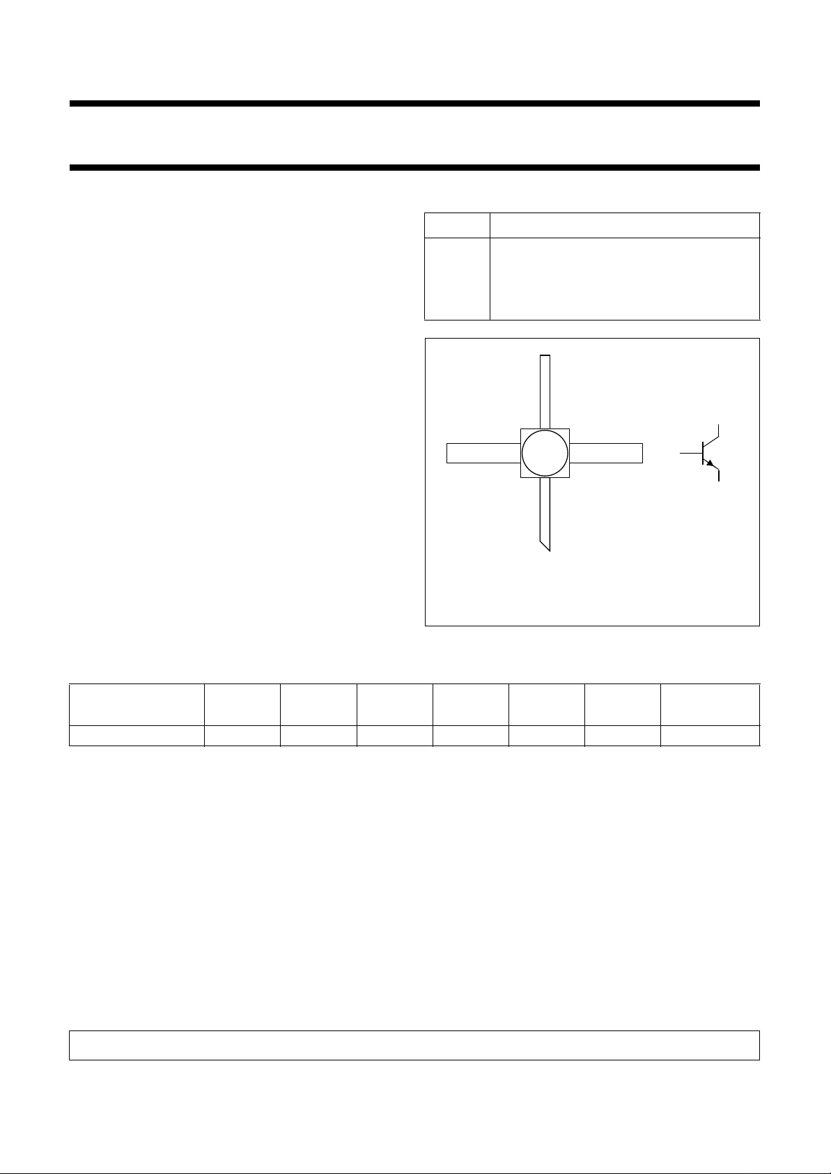
PINNING - SOT100
PIN DESCRIPTION
1 collector
2 emitter
3 base
4 emitter
handbook, halfpage
2
Marking code: R9.
3
1
Fig.1 Simplified outline and symbol.
c
4
b
e
MAM312
QUICK REFERENCE DATA
RF performance up to T
MODE OF
OPERATION
=25°C in a common emitter class A circuit.
case
f
(GHz)
V
(V)
CE
I
C
(mA)
P
L1
(mW)
G
po
(dB)
Z
(Ω)
i
Z
L
(Ω)
CW linear amplifier 4 18 30 >126 >7.5 typ. 4 + j23 typ. 6.5 + j32
MAINTENANCE TYPE - NOT RECOMMENDED FOR NEW DESIGNS; SEE INDEX SECTION OF SC15
1997 Feb 18 2

Philips Semiconductors Product specification
NPN microwave power transistor LAE4002S
LIMITING VALUES
In accordance with the Absolute Maximum Rating System (IEC 134).
SYMBOL PARAMETER CONDITIONS MIN. MAX. UNIT
V
CBO
V
CER
V
CEO
V
EBO
I
C
P
tot
T
stg
T
j
T
sld
Note
1. Up to 0.1 mm from ceramic.
collector-base voltage open emitter − 40 V
collector-emitter voltage RBE= 220 Ω−35 V
collector-emitter voltage open base − 16 V
emitter-base voltage open collector − 3V
collector current (DC) − 90 mA
total power dissipation T
≤ 75 °C − 625 mW
case
storage temperature −65 +200 °C
junction temperature − 200 °C
soldering temperature t ≤ 10 s; note 1 − 235 °C
2
10
handbook, halfpage
I
C
(mA)
(1)
10
1
11010
T
≤ 75 °C; RBE< 220Ω.
case
(I) Second breakdown limit (independent of temperature).
VCE (V)
Fig.2 DC SOAR.
MGD998
2
800
handbook, halfpage
P
tot
(mW)
600
400
200
0
0 50 100 200
150
T
case
Fig.3 Power derating curve.
MGD997
o
(
C)
MAINTENANCE TYPE - NOT RECOMMENDED FOR NEW DESIGNS; SEE INDEX SECTION OF SC15
1997 Feb 18 3
 Loading...