

Page 1

1
Colour Television Chassis
L9.1A
AA
CL 86532104_006.eps
300399
ServiceManual
Table of contents Page
1. Technical specifications 2
2. Connection facilities and chassis overview 3
3. Safety and maintenance instructions 5
4. Mechanical instructions 7
5. Faultfinding and repair tips 8
6. Fault finding trees 15
Supply voltages diagram 19
Blockdiagram 20
Testpoint overviews 21
7. Electrical Diagrams and print lay-outs
Diagram PWB
Power supply diagram A1 22 30,32 Diversity tables 23 30,32 Horizontal deflection diagram A2 24 30,32 Vertical deflection diagram A3 25 30,32 Synchronisation diagram A4 26 30,32 Tuner and VIF diagram A5 27 30,32
Published by JR9964 TV Service DepartmentPrinted in The NetherlandsCopyright reserved 1999 Philips Consumer Electronics B.V. Eindhoven, The Netherlands. All rights reserved. No part of this publication may be reproduced, stored in a retrieval system or transmitted, in any form or by any means, electronic, mechanical, photocopying, or otherwisewithout the prior permision of Philips.Subject to modification5 4822 727 21704
Video processing diagram A6 28 30,32 Control diagram A7 29 30,32 Front Control diagram A8 31 30,32 BTSC Decoder diagram A9 34 30,32 NICAM/2CS diagram A10 35 30,32 Smart Sound diagram A11 37 30,32 Audio amplifier diagram A12 36 30,32 Headphone diagram A13 37 30,32 Rear IO Cinch diagram A14 38 30,32 CRT panel diagram B 39 40 Side AV diagram E 33 33
8. Alignments 41
9. Circuit description new circuits 46
10. Directions for use 52
11. List of abbreviations 61
12. Spare parts list 63
©
Copyright reserved 1999 Philips Consumer Electronics B.V. Eindhoven, The
Netherlands. All rights reserved. No part of this publication may be reproduced,
stored ina retrievalsystem ortransmitted, in any form or by any means, electronic, mechanical, photocopying, or otherwise without the prior permision of Philips.
Published by JR9964 TV Service Department Printed in The Netherlands Subject to modification 5 4822 727 21704
Page 2

2 L9.1A
1 Technical Specifications
Mains voltage : 90V - 276Vac; Mains frequency : 50 - 60Hz Maximum power consumption : 25" : 75W +/- 10%
Standby power consumption : 7W +/- 10% Colour Synchronisation : Sub-carrier pull in range : +/- 300Hz for NTSC : +/- 250Hz Horizontal Synchronisation : Catching range : +/- 600 Hz Holding range : +/- 1200 Hz Vertical Locking Range : 49 Hz - 61Hz Tuners : UV 1316/AI-2 (PAL)
1 Technical Specifications
: 29" : 90W +/- 10%
: UV 1316/AIU-2 (PAL)
: UV1356C/AI ( PAL)
: TEDH9X001 (NTSC)
Page 3
2 Connection facilities and chassis overview
2 Connection facilities and chassis overview
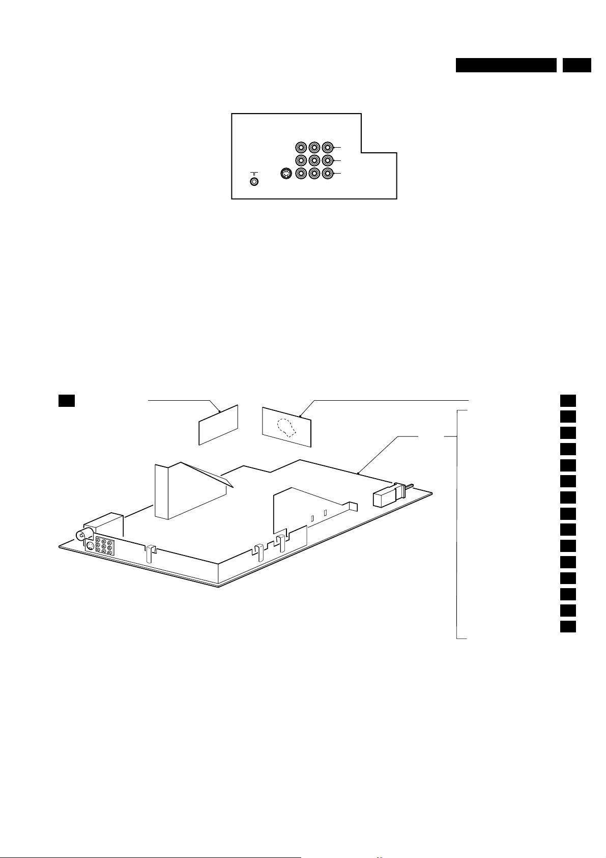
2.1 Specification of the terminal sockets
Video
S-Video
IN OUTIN
L
Audio
R
3L9.1A
Figure 2-1
2.1.1 Inputs (AV1, AV2 and Side AV)
- Cinch CVBS (yellow)(1Vpp +/- 3dB 75Ω) q
- Cinch Audio R (red) (0.2-2VRMS 10kΩ) q
- Cinch Audio L (white) (0.2-2VRMS 10kΩ) q
2.1.2 Outputs (MONITOR out)
- Cinch CVBS (yellow) (1Vpp +/- 3dB 75Ω) q
- Cinch Audio R (red) (0.5VRMS < 1kΩ) q
- Cinch Audio L (white) (0.5VRMS < 1kΩ) q
SIDE AV PANEL
E
Figure 2-2
CL 86532104_069.AI
290399
2.1.3 Headphone
- Jack 8-600Ω (4mW) t
2.1.4 SVHS
1- Ground v 2- Ground v 3- Y (1Vpp +/- 3dB 75Ω) p 4- C (0.3Vpp +/- 3dB 75Ω) p
2.2 PCB location drawing
CRT PANEL
POWER SUPPLY
MAIN
CHASSIS
PANEL
HOR.DEFLECTION
VERT. DEFLECTION
SYNCHRONISATION
TUNER + VIDEO IF
VIDEO PROCESSING
CONTROL (µC)
FRONT CONTROLS
BTSC DECODER (RES)
NICAM + 2CS DECODER
SMART SOUND
AUDIO AMPLIFIER
HEADPHONE
I/O CINCH
CL 86532104_004ap.eps
B
A1
A2
A3
A4
A5
A6
A7
A8
A9
A10
A11
A12
A13
A14
010499
Page 4

4 L9.1A
3 Safety and maintenance instructions
3 Safety and maintenance instructions
3.1 Safety instructions for repairs
Figure 3-1
1. Safety regulations require that during a repair: – the set should be connected to the mains via an
isolating transformer;
– safety components, indicated by the symbol (see fig.
3.1), should be replaced by components identical to
the original ones;
– when replacing the CRT, safety goggles must be worn.
2. Safety regulations require that after a repair the set must
be returned in its original condition. In particular attention
should be paid to the following points.
– As a strict precaution, we advise you to resolder the
solder joints through which the horizontal deflection
current is flowing, in particular:
• all pins of the line output transformer (LOT);
• fly-back capacitor(s);
• S-correction capacitor(s);
• line output transistor;
• pins of the connector with wires to the deflection coil;
• other components through which the deflection current flows.
Note: This resoldering is advised to prevent bad
connections due to metal fatigue in solder joints and is
therefore only necessary for television sets older than
2 years. The wire trees and EHT cable should be
routed correctly and fixed with the mounted cable
clamps.
– The insulation of the mains lead should be checked for
external damage.
– The mains lead strain relief should be checked for its
function in order to avoid touching the CRT, hot
components or heat sinks.
– The electrical DC resistance between the mains plug
and the secondary side should be checked (only for
sets which have a mains isolated power supply). This
check can be done as follows:
• unplugthe mains cord and connect a wire between the two pins of the mains plug;
• set the mains switch to the on position (keep the mains cord unplugged!);
• measure the resistance value between the pins of
the mains plug and the metal shielding of the tuner
or the aerial connection on the set. The reading
should be between 4.5 MΩ and 12 MΩ;
• switch off the TVand remove the wire between the two pins of the mains plug.
– The cabinet should be checked for defects to avoid
touching of any inner parts by the customer.
3.2 Maintenance instruction
It is recommended to have a maintenance inspection carried
out by a qualified service employee. The interval depends on
the usage conditions:
– When the set is used under normal circumstances, for
example in a living room, the recommended interval is 3 to
5 years.
– When the set is used in circumstances with higher dust,
grease or moisture levels, for example in a kitchen, the
recommended interval is 1 year.
– The maintenance inspection contains thefollowing actions:
• Execute the above mentioned 'general repair instruction'.
• Clean the power supply and deflection circuitry on the chassis.
• Cleanthepicturetubepanelandthe neck of the picture tube.
3.3 Warnings
1. ESD All ICs and many other semiconductors are susceptible to electrostatic discharges (ESD). Careless handling during repair can reduce life drastically. When repairing, make sure that you are connected with the same potential as the mass of the set by a wristband with resistance. Keep components and tools also at this same potential. – complete kit ESD3 small table mat, wristband,
connectionbox, extensioncable and earthcable 4822
310 10671
– wristband tester 4822 344 13999
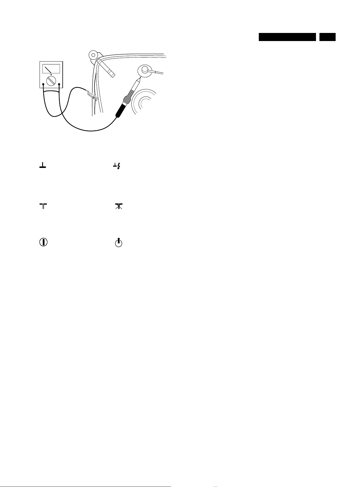
2. In order to prevent damage to ICs and transistors, all highvoltage flashovers must be avoided. In order to prevent
damage to the picture tube, the method shown in Fig. 3.2
should be used to discharge the picture tube. Use a highvoltageprobe and a multimeter (positionDC-V). Discharge
until the meter reading is 0V (after approx. 30s).
3. Togetherwith the deflection unit and anymultipole unit, the
flat square picture tubes used from an integrated unit. The
deflection and the multipole units are set optimally at the
factory.Adjustmentofthisunit during repair is therefore not
recommended.
4. Be careful during measurements in the high-voltage section and on the picture tube.
5. Never replace modules or other components while the unit is switched on.
6. When making settings, use plastic rather than metal tools.
This will prevent any short circuits and the danger of a
circuit becoming unstable.
7. Wearsafety goggles during replacement ofthe picture tube
3.4 Notes
1. The direct voltages and oscillograms should be measured
with regard to the tuner earth , or hot earth as this is called
(see fig. 3.3)
2. The direct voltages and oscillograms shown in the
diagrams are indicative and should be measured in the
Service Default Mode (see chapter 8) with a colour bar
signal and stereo sound (L:3 kHz, R:1 kHz unless stated
otherwise) and picture carrier at 475.25 MHz.
3. Wherenecessary, the oscillograms and directvoltages are
measured with and without aerial signal. Voltages in the
power supply section are measured both for normal
operation and in standby . These values are indicated by
means of the appropriate symbols (see fig. 3.3).
4. The picture tube PWB has printed spark gaps. Each spark
gap is connected between an electrode of the picture tube
and the Aquadag coating.
5. The semiconductors indicated in the circuit diagram and in
the parts lists are completely interchangeable per position
with the semiconductors in the unit, irrespective of the type
indication on these semiconductors.
Page 5
3 Safety and maintenance instructions
a
V
CL 26532098/042
140792
Figure 3-2
5L9.1A
tuner earth
tuner aarde
la masse du tuner
Tuner-Erde
massa del tuner
tierra del sintonizador
with aerial signal
met antenne signaal
avec signal d'antenne
mit Antennensignal
con segnale d'antenna
con la señal de antena
normal condition
normaal bedrijf
fonctionnement normal
normaler Betrieb
funzionamento normale
funcionamiento normal
hot earth
hete aarde
la terre directe
heißen Erde
massa calda
tierra caliente
without aerial signal
zonder antenne signaal
sans signal d'antenne
.ohne Antennensignal
senza segnale d'antenn
sin la señal de antena
stand by
stand by
position de veille
in Bereitschaft
modo di attesa
posición de espera
Figure 3-3
Page 6
6 L9.1A
4 Mechanical instructions
4 Mechanical instructions
4.1 Service positions
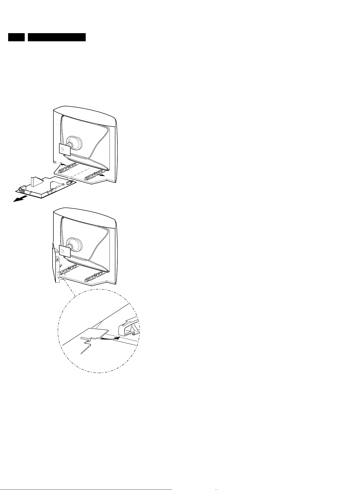
See figure 4.1 for the service position.
1. Disconnect the connecting cable feeding the right-hand
speaker, also disconnect the degaussing cable.
A
1
1
1
2
2. The mono-carrier is removed by pushing the two centre
clips (1) at both chassis brackets outwards and pulling the
panel forward. (2)
3. Flip the mono-carrier over so that the component side of the board faces towards the CRT.
4. Slide the metal heat sink underneath the left chassis
bracket (3) until the carrier is locked in position.
B
Figure 4-1
3
CL 86532104_007.ai
170299
Page 7

5 Fault finding and repair tips
5 Fault finding and repair tips
This chapter includes information covering:
5.1 Test points
5.2 Service Modes and Dealer Service Tool (DST)
5.3 The menus and submenus
5.4 Error code buffer and error codes
5.5 The "blinking LED" procedure
5.6 Trouble shooting tips
5.7 Customer Service Mode ( CSM )
5.8 Computer Aided Repair ( ComPair )
5.9 Ordering ComPair
5.1 Test points
The L9 chassis is equipped with easily identifiable test points.
These are clearly marked on the PCB. The test points refer to
specific functional blocks, these are:
• A1-A2-A3, etc.: Test points for the BTSC decoder (A9),
Nicam + 2CS decoder (A10) and Audio Amplifier (A12)
• C1-C2-C3, etc.: Test points for the control circuit (A7)/ front control ( A8 )
• F1-F2-F3, etc.: Test points for the vertical deflection circuit (A3)
• I1-I2-I3, etc.: Test points for the tuner + Video IF circuit (A5)
• L1-L2-L3, etc.: Test points for the horizontal deflection circuit (A2)
• P1-P2-P3, etc.: Test points for the power supply (A1)
• S1-S2-S3, etc.: Test points for the synchronisation circuit (A4)
• V1-V2-V3, etc.: Test points for the video processing circuitry (A6) / CRT panel (B)
Measurements are performed under the following conditions:
Video: colour bar signal; audio: 3kHz left, 1kHz right
5.2 Service modes and Dealer Service Tool (DST)
7L9.1A
• Used to provide a pre-defined situation (pre-defined
parameters), so that the same measurements can be
obtained as per the service manual.
• Overrides the 5V protection when the internal method of
SDM is used (connecting together pin M24 and pin M25).
• starts the LED flashing procedure
• Setting up of options codes
• Inspect the error buffer
Entering the SDM:
– Bytransmitting the "DEFAULT" command with the RC7150
Dealer Service Tool (this works both while the set is in
normal operation mode or in the SAM)
– Standard RC sequence 062596 followed by the key
"MENU"
– By connecting test-pins M25 and M24 together (on the
mono-carrier)while switching on the set. Afterswitchingon
the set the link should be removed ( Caution!! By entering
the SDM mode you override the 5V protections ).
Exit the SDM:
Switch the set to Standby or press EXIT on the DST (the error buffer is also cleared).
Note: When the mains power is switched off while the set is in
SDM, the set will switch to SDM immediately when the mains
is switched on again. ( The error buffer will not be cleared ).
The SDM sets the following pre-defined conditions:
• Pal/Secam sets: tuning at 475.25 PAL
• NTSC sets : tuning channel 3 at 61.25MHz
Volume level is set to 25% (of the maximum volume level).
Other picture and sound settings are set to 50%. The following
functions are "ignored" in SDM since they interfere with
diagnosing/repairingaset. "Ignoring" means that the event that
is triggered is not executed, the setting remains unchanged.
For easy installation and diagnosis, the dealer service tool
(DST) RC7150 can be used. When there is no picture (to
accesstheerrorcodebuffer via the OSD). The DST can enable
to set to display the entire contents of the error code buffers by
using the flashing LED procedure.
Important Note: The L9 does not incorporate two way Infra red communication.
The part number for the DST (RC7150) is 4822 218 21232.
5.2.1 Installation features for the dealer
The dealer can use the RC7150 for programming the TV-set
with presets. 10 Different program tables can be programmed
into the DST via a GFL TV, MD or MG set (downloading from
the TV to the DST; for example see the GFL service manuals).
For an explanation of the installation features of the DST,
please see the directions of use for use of the DST (for the L9
chassis, download code 4 should be used).
5.2.2 Diagnosis features for the servicer
L9 models can be put into either of the two available service
modes by using the RC7150. These are the Service Default
Mode (SDM) and the Service Alignment Mode (SAM).
5.2.3 Service Default Mode (SDM)
The purpose of the SDM is:
• (Sleep)Timer
• Blue mute
• Auto switch off
• Hotel or Hospitality Mode
• Child lock or Parental lock
• Skipping, blanking of "Not favourite" present/channels
• Automatic storing of Personal Preset settings
• Automatic user menu time-out
All other controls operate normally.
5.2.4 Special functions in SDM
Access to normal user menu
Pressing the "MENU" button on the remote control will enter
thenormal user menu (TV lock, Installation, Brightness, colour
andcontrast)while"SMD"remainsdisplayed intopofscreen).
Pressing the "MENU" key again will return to the last SDM
status.
Error buffer
Pressingthe"OSD" button of the remote control shows all OSD (incl. error buffer).
Access to SAM
By pressing the "CHANNEL DOWN" and "VOLUME DOWN"
buttons on the local keyboard simultaneously the set switches
from SDM to SAM or pressing "ALIGN" on the DST
Page 8
8 L9.1A
5 Fault finding and repair tips
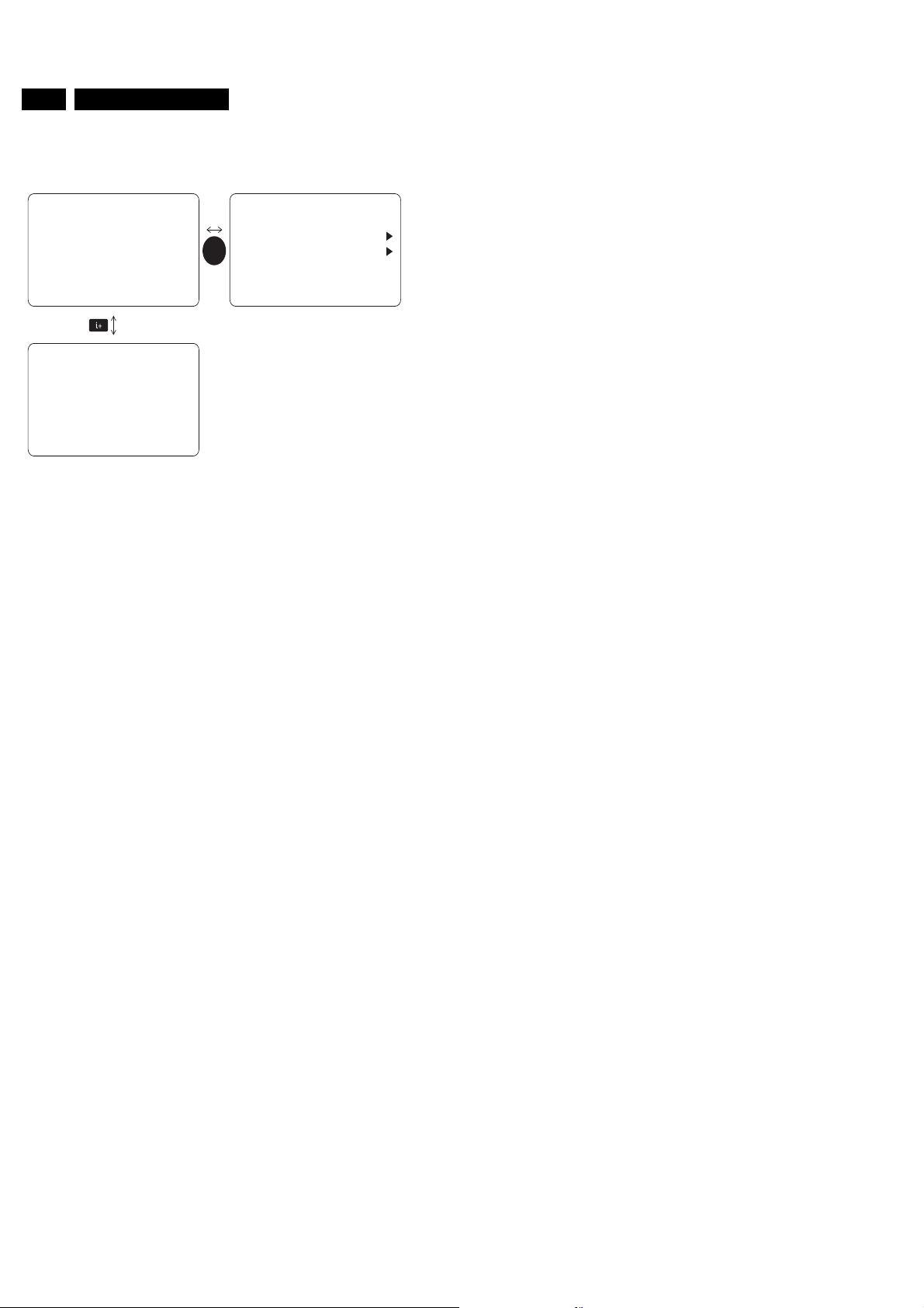
In the SDM the following information is displayed on the screen:
LLLL L90BBC X.Y SDM
OP VALUE
OB1 OB2 OB3 OB4 OB5 OB6 OB7
ERR xx xx xx xx xx
SDM
TV LOCK
MENU
INSTALLATION
BRIGHTNESS
COLOUR
CONTRAST
llllll
llllll
llllll
CL 86532104_015.eps
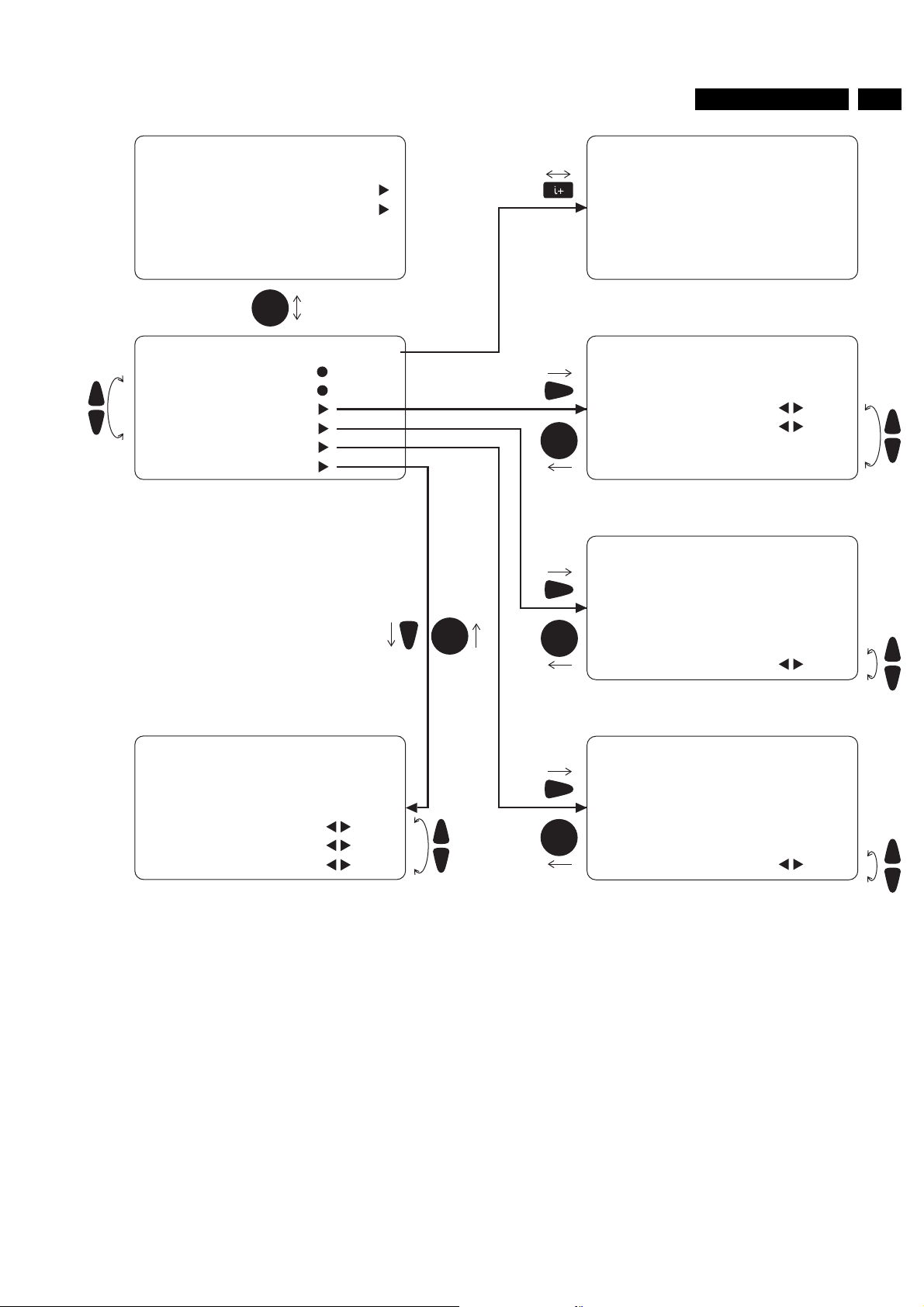
Figure 5-1 : Service Default Mode screens and
structure
Explanation notes/references:
(1) "LLLL" Operation hours timer (hexadecimal)
(2)Softwareidentificationofthemainmicrocontroller(L90BBC X.Y)
• L90 is the chassis name for L9.0E
• BBC is a 2 letter and 1 digit combination that indicates the
software type and the supported languages:
• X = (main version number)
• Y = (subversion number) BB = (range specification )
......
......
......
SDM
31
31
31
160299
5.2.5 Service Alignment Mode (SAM)
The SAM allows adjustment of the Demodulator I.F, align the
white tone, adjust the picture geometry and sound
adjustments.
For easy identification of the SAM mode, "SAM" is displayed
in the top of the right side of the screen
Entering SAM:
– By transmitting the "ALIGN" command with the RC7150
Dealer Service Tool
– By pressing the "CHANNEL DOWN" and "VOLUME
DOWN" key on the local keyboard simultaneously when
the set is in SDM
– Standard RC sequence 062596 followed by the key "OSD"
– By shorting test-pins M28 and M29 on the mono-carrier
while switching on the set. After switching on the set the
short-circuit can be removed. ( Caution!! Override of 5V
protections ).
Exiting the SAM:
Switch the set to standby or press EXIT on the DST (the error buffer is cleared).
Note: When the mains power is switched off while the set is in
SAM, the set willswitch to SAM immediatelywhen the mains is
switched on again. ( The error buffer will not be cleared ).
Inthe SAM the followinginformation is displayed on thescreen:
(3) "SDM" To indicate that the TV set is in de service mode
(4) "OP" Options Code consist of 2 characters. It is possible to change each option code
"VALUE" The value of the selected option ( ON/OFF or a combination of 2 letters )
"XXX" Value of the options bytes ( OB1 .. OB7)
"ERR" The last five detected errors; The left most number indicates the most recent error detected.
The MENU UP or MENU DOWN command can be used to
select the next/previous option; The MENU LEFT and MENU
RIGHT command can be used to change the option value.
Remark: When the option-code RC = OFF, theP+ and the Pkey have the same functions as the MENU UP/DOWN keys
while the VOL+ and the VOL- key have the same function as
the MENU LEFT/RIGHT keys. It is not possible to change the
channel pre-set or to adjust the volume when in SAM/SDM
menu when the option RC = OFF.
Using a L9 remote control, option-code RC = ON, the P+, P-,
VOL- and VOL+ can be used to change the pre-set and/or to
adapt the volume, while the menu-cursor keys are used to
select the option and to change its value.
For an extended overview of the option codes see Chapter 8 Options
Page 9
5 Fault finding and repair tips
9L9.1A
TV LOCK
INSTALLATION
BRIGHTNESS
COLOUR
CONTRAST
AKB
VSD
TUNER
WHITE TONE
GEOMETRY
AUDIO
MENU
llllll
llllll
llllll
......
......
......
SAM
31
31
31
SAMAAABBC X.Y
MENU
L90 BBC X.Y
TUNER
IF-PLL
IF-PLL POS
AFA
AFB
L90 BBC X.Y
SAM
SAM
64
192
1
1
SAM
A-FM
AT
STEREO
L90 BBC X.Y
SOUND
SAM
232
15
MENU
MENU
NORMAL RED
40
SAM
L90 BBC X.Y
4
MENU
VAM
55
Figure 5-2 : Service Alignment Mode screens and
structure
CL 86532104_016.eps
030399
Page 10

10 L9.1A
5 Fault finding and repair tips
Access to normal user menu
Pressing the "MENU" button on the remote control will enter
the normal user menu ( TVlock, installation, brightness, colour
and contrast ) while "SAM" remains displayed in top of screen.
Pressing the "MENU" key again will return to the last SAM
status.
Pressing the "OSD" button of the remote control shows only "SAM" in the top of screen
Access to SDM
Pressing the "DEFAULT" button on the DST
SAM menu control
Menu items (AKB, VSB, Tuner, White tone, Geometry and
Sound) can be selected with the MENU Up or MENU DOWN
key. Entry into the selected items (sub menus) is done by the
MENU LEFT or MENU RIGHT key. The selected item will be
highlighted.
With the cursor LEFT/RIGHT keys, it is possible to increase/ decease the value of the selected item.
5.3 The menus and submenus
5.3.1 Tuner sub menu
The tuner sub menu contains the following items:
–
– IF_PLL: PLL Alignment for all PAL/SECAM systems
– AFW: AFC Window
– AGC: AGC take-over point
– YD: Default value = 12 ; Do not align
– CL: Default value = 4 ; Do not align
– AFA
– AFB
The items AFA and AFB can not be selected, they are for monitoring purposes only.
The commands MENU UP and MENU DOWN are used to select the next/previous item.
The commands MENU LEFT and MENU RIGHT are used to
increase/decreasethe value of the selected item. Thechanged
values will be send directly to the related hardware.
The item values are stored in NVM if this sub menu is left.
The commands MENU LEFT and MENU RIGHT are used to
increase/decreasethe value of the selected item. Thechanged
values will be send directly to the related hardware.
The item values are stored in NVM if this sub menu is left.
The Contrast Plus feature (black stretch) is set to OFF when the white tone submenu is entered.
5.3.3 Audio sub menu
The tuner sub menu contains the following items:
– AF-M: Default value = 232 ; Do not align
– AT: Default value = 4 ; Do not align
– STEREO: Default value = 15 ; Do not align
– DUAL: Default value = 12 ; Do not align
The sound adjustments sub menu is not available in Mono sets.
The presence of an item in the menu is dependent on the selected soundboard (option SB).
The commands MENU UP and MENU DOWN are used to select the next/previous item.
The commands MENU LEFT and MENU RIGHT are used to
increase/decreasethe value of the selected item. Thechanged
values will be sent directly to the related hardware.
The item values are stored in NVM if this sub menu is left.
5.3.4 Geometry sub menu
The geometry sub menu contains the following items:
– SBL : Service blanking
– VSL : Vertical slope
– VAM : Vertical amplitude
– VSH : Vertical shift
– HSH : Horizontal shift
– VSC : Vertical S correction
– H60 : Default value = 10 ; Do not align
– V60 : Default value = 12 ; Do not align
– EWC : E-W corner
– EWT : E-W trapezium
– EWP : E-W parabola
– EWW : E-W width
5.3.2 White tone sub menu
The white tone sub menu contains the following items:
– NORMAL RED
– NORMAL GREEN
– NORMAL BLUE
– DELTA COOL RED
– DELTA COOL BLUE
– DELTA COOL GREEN
– DELTA WARM RED
– DELTA WARM BLUE
– DELTA WARM GREEN
OSD is kept to a minimum in this menu, in order to make white tone alignment possible.
The commands MENU UP and MENU DOWN are used to select the next/previous item.
5.4 Error code buffer and error codes
5.4.1 Error code buffer
The error code buffer contains all errorsdetected since thelast
time the buffer was erased. The buffer is written from left to
right.
– whenanerroroccursthat is not yet in the error code buffer,
the error is written at the left side and all other errors shift
one position to the right
– the error code buffer will be cleared in the following cases:
1. exiting SDM or SAM with the "Standby" command on the remote control
2. transmitting the commands "EXIT" with the DST (RC7150)
3. transmitting the commands "DIAGNOSE-9-9-OK" with the DST.
– By leaving SDM or SAM with the mains switch, the error
buffer is not reset.
Page 11

5 Fault finding and repair tips
11L9.1A
Examples:
ERROR: 0 0 0 0 0 : No errors detected
ERROR: 6 0 0 0 0 : Error code 6 is the last and only detected error
ERROR: 5 6 0 0 0 : Error code 6 was first detected and error
code 5 is the last detected (newest) error
5.4.2 Error codes
In the case of non-intermittent faults, clear the error buffer
before starting the repair to prevent "old" error codes being
present. If possible check the entire contents of the error
buffers.In some situations an errorcode is only the RESULT of
another error code (and not the actual cause).
Note: a fault in the protection detection circuitry can also lead to a protection.
Error 0 = No error
Error 1 = X-ray ( Only for USA sets )
Error 2 = High beam current protection and E/W Horizontal protection
Highbeam protection active; set is switchedto protection; error
code 2 is placed in the error buffer; the LED will blink 2 times (
repeatedly ).
As the name implies, the cause of this protection is a too high
beam current (bright screen with flyback lines). Check whether
the +200V supply to the CRT panel is present. If the voltage is
present, the most likely cause is a fault on the CRT panel.
DisconnecttheCRTpaneltodetermine the cause. If the +200V
voltage is not present, check R3340 ( CRT panel - B ), R3485
and D6485 ( Horizontal Deflection - A2 )
EW protection:
If this protection is active, the causes could be one of the following;
Sound processor does not respond to the micro controller
Error 5 = Bimos start-up error ( POR bit )
Bimos start-up register is corrupted or the I2Cline to the Bimos
is always low or no supply at pin 12 of the Bimos). This error is
usually detected during start-up and hence will prevent the set
from starting up.
Error 6 = Bimos (TDA884x) I2C error
Note that this error may also be reported as a result of error
codes 4 (in that case the Bimos might not be the actual
problem)
Error 7 = General I2C error. This will occur in the following cases:
• SCL or SDA is shorted to ground
• SCL is shorted to SDA
• SDA or SCL connection at the micro controller is open circuit.
Error 8 = Microprocessor internal RAM error
The micro controller internal RAM test indicated an error of the
micro controller internal memory (tested during start-up);
Error 9 = EEPROM Configuration error ( Checksum error ); EEPROM is corrupted.
Error 10 = I2C error EEPROM error. NV memory (EEPROM) does not respond to the micro controller
Error 11 = I2C error PLL tuner. Tuner is corrupted or the I2C
line to the Tuner is low or no supply voltage present at pin 9,
pin 6 or pin 7 of the tuner.
Error 12 = Black current loop instability protection. The black
current could not be stabilised. The possible cause could be a
defect in one or moreof the RGB amplifiers,RGB guns or RGB
driving signals.
5.5 The "blinking LED" procedure
– horizontal deflection coil 5445
– linearity coil 5457
– S-correction capacitor 2466/2468
– flyback capacitor 2465
– line output stage
– short circuit of:
– flyback diode 6460
– EW transformer (bridge coil) 5465/5470 or 5463/5471
(version dependent)
– S-correction capacitor 2457
– EW power-transistor 7460 or driver-transistor 7461
Error 3 = Vertical / Frame protection
There are no pulses detected at pin 47 of the main microprocessor 7600 ( panel A7 ).
If this protection is active, the causes could be one of the following items;
– IC 7401 is faulty
– Open circuit of vertical deflection coil
– Vlotaux +11V not present and/or Vlotaux -11V not present
– Resistor 3409
Error4 = Sound processor I2C error (MSP3415Dor MSP3435 or BSP3501 )
The contents of the error buffer can also be made visible via
the "blinking LED" procedure. This is especially useful when
there is no picture. There are two methods of access:
1. When the SDM is entered, the LED will blink thenumber of
times, equal to the value of the error codes in the errorbuffer, starting with the first error-code, pause, second
error-code, pause etc. (repeatedly).
2. With the DST all error codes in the error buffer can be
made visible. Transmit the command: "DIAGNOSE x OK"
where x is theposition in the error buffer to be made visible
x ranges from 1, (thelast (actual) error) to6 (the first error).
TheLEDwill operate in the same way as in point1, butnow
for the error code on position x.
Example:
Error code position: 1 2 3 4 5
Error buffer: 8 9 5 0 0
• after entering SDM: blink (8x) - pause - blink (8x) - etc.
• after transmitting "DIAGNOSE- 2- OK" with the DST blink (9x) - pause - blink (9x) - etc.
• after transmitting "DIAGNOSE- 3- OK" with the DST blink(5x) - pause - blink(5x) - etc.
Page 12

12 L9.1A
5 Fault finding and repair tips
• after transmitting "DIAGNOSE- 4- OK" with the DST nothing happens
5.6 TROUBLE SHOOTING TIPS
In this paragraph some trouble shooting tips for the deflection
and power supply circuitry are described. For detailed
diagnostics, use the fault finding tree or use ComPair.
5.6.1 THE DEFLECTION CIRCUIT:
1. Check that the +VBATT ( 140V) is present across 2551 (
A1 POWER SUPPLY ). If the voltage is not present,
disconnect coil 5551 ( A1 Power Supply) (Horizontal
deflection stage is disconnected). If the voltage is present
then the fault might be caused by the deflection circuit.
Possible Candidates Are:
– Transistor 7460 is faulty
– The driver circuit around transistor 7461 is faulty
– No horizontal drive signal coming from the BIMOS
7250-D pin 40 ( A4 - Synchronisation )
2. Note: If the Collector of 7460 is shorted to the Emitter, a
tripping noise will be heard from the power supply circuit.
3. To determine whether the fault is present in the horizontal
deflection circuit or in the E/W circuit ( A2 - Horizontal
Deflection ), de-solder jumper 9465 and insert a jumper
into position number 9461. This disables the E/W
protection.Ifthe basic deflection stage now works correctly
( parabolic picture) then the fault is present in the E/W
circuit. If there is still no horizontal deflection, then the fault
is present in the basic deflection circuitry.
4. Also don't forget the protection circuits in the line output
stage. If any of these circuits are activated, the setwill shut
down. Depending on the protection, the led will blink
according to the fault defined. In order to determine which
protection circuit is active, isolationof each separate circuit
is necessary. These protection circuits are:
– High beam current protection ( LED blinks repetitively
2 times ) - CRT panel ( B )
– E/W Horizontal protection ( LED blinks repetitively 2
times ) - Horizontal deflection ( A2 )
– Vertical protection ( LED blinks repetitively 3 times ) -
Vertical deflection ( A3 )
5.6.2 THE POWER SUPPLY
5.7 Customer Service Mode (CSM)
All L9.1 sets are equipped with the "Customer Service Mode"
(CSM). CSM is a special service mode that can be activated
and deactivated by the customer, following a request from the
service technician/dealer perhaps during a telephone
conversation to identify the status of the set. This CSM is a
'read only' mode, therefore modifications or changes while the
set is in this mode are not possible.
Entering the Customer Service Mode. The Customer Service
Mode can be switched on by pressing simultaneously the
button (MUTE) on the remote control and any key on the
control buttons (P+, P-, VOL +, VOL -) on the TV for at least 4
seconds.
When the CSM is activated:
• picture and sound settings are set to nominal levels
• "Service unfriendly modes" are ignored
Exit the Customer Service Mode.
The Customer Service Mode will switch off after:
– pressing any key on the remote control handset (except
"P+" or "P-")
– switching off the TV set with the mains switch.
All settings that were changed when CSM was activated are set back to the initial values
5.7.1 The Customer Service Mode information screen
The following information is displayed on screen:
• Line number for every line (to make CSM language independent)
• Operating hours
• Software version L90BBC X.Y)
• Text "CSM" on the first line
• Error buffer contents
• Option code information
• Configuration information
• Service unfriendly modes
To trouble shoot the L9 SMPS, first check the Vaux voltage on
C2561. If this voltage is not present, check fuse F1572 and
D6560.IfF1572orD6560is not open circuit, the problem might
be caused on the primary side of the switching supply. Check
theoutputofthe bridge rectifier on the C2508 for approximately
300V DC. If this voltage is missing, check the bridge rectifier
6505 and the fuse 1500. If fuse F1500 is found to be open
circuit, check MOSFET 7518 to make sure that there is no
short circuit present and check R3518. If the 300V DC is
present on C2508, check for a start-up voltage of approx. 13V
on pin 1 of IC7520. If no start-up voltage is present, check if
R3510 is open; zener 6510 is a short-circuit. It is necessary to
have a feedback signal from the hot primary side of switch
modetransformerT5545at pin 8 and pin 9 for the power supply
to oscillate. If this start-up voltage ispresent on pin 1 of IC7520
and the supply is not oscillating, check R3529 and D6540.
Check for a drive signal at the gate of MOSFET 7518, square
wave signal - P2. Check pin 3 of IC7520, R3525 and D6514
To determined whether OVP is active, check whether Vaux is present at C2561.
1 HHHH L90BBC-X.Y CSM
2 CODES xx xx xx xx xx
3 OP xxx xxx xxx xxx xxx xxx xxx
4 SYS: xxxxxxxxxxx
5 NOT TUNED
6 TIMER
7 LOCKED
8 (HOSPITAL) (HOTEL)
9 VOL LIM <value>
CL 86532104_014.eps
080299
Figure 5-3 : Screen lay-out Customer Service Mode
SYS:xxxxxx = xxxxxx is the SYSTEMTHAT IS SET FOR THIS PRESET
NOT TUNED = no ident signal present
TIMER = (SLEEP) TIMER is activated
LOCKED = Channel/preset locked via parental lock, child lock
Page 13

5 Fault finding and repair tips
13L9.1A
HOTEL = HOTEL mode activated; HOSPITAL = HOSPITAL mode activated
VOL LIM > = Volume limiter activated and set to >
5.7.2 Exit
Any key (RC or local keyboard) except "channel up" / "channel
down" (standby switched to standby, mains OFF switches set
off, other keys switch to normal operation)
5.8 ComPair
5.8.1 Introduction
ComPair (Computer Aided Repair) is a service tool for Philips
Consumer Electronics products. ComPair is a further
developmenton the DST service remote control allowingfaster
and more accurate diagnostics. ComPair has three big
advantages:
• ComPair helps you to quickly get an understanding how to
repair the L9.1A in short time by guiding you step by step
through the repair procedures.
• ComPair allows very detailed diagnostics (on I2C level)
and is therefore capable of accurately indicating problem
areas. You do not have to know anything about I2C
commands yourself; ComPair takes care of this.
• ComPair speeds up the repair time since it can
automaticallycommunicatewiththe L9.1A (when the micro
processor is working) and all repair information is directly
available. When ComPair is installed together with the
SearchMan L9.1A electronic manual, schematics and
PCBs are only a mouse-click away.
ComPair consists of a Windows based fault finding program
and an interface box between PC and the (defective) product.
The ComPair interface box is connected to the PC via a serial
or RS232 cable. In case of the L9.1A chassis, the ComPair
interface box and the L9 communicate via an I2C cable (bidirectional) and via infra red communication (uni-directional;
from ComPair interface box to L9.1A)
The ComPair fault finding program is able to determine the
problem of the defective television. ComPair can gather
diagnostic information in 2 ways:
1. Communication to the television (automatic)
2. Asking questions to you (manually)
ComPair combines this information with the repair information
in its database to find out how to repair the L9.1A.
Automatic information gathering
Reading out the error buffer, ComPair can automatically read
out the contents of the entire error buffer.
Diagnosis on I2C level. ComPair can accessthe I2C busof the
television. ComPair can send and receive I2C commands to
themicrocontroller of the television. In this wayit ispossible for
ComPair to communicate (read and write) to devices on the
I2C busses of the L9.1A.
Manual information gathering
Automatic diagnosis is only possible if the micro controller of
the television is working correctly and only to a certain extend.
When this is not the case, ComPair will guide you through the
fault finding tree by asking you questions and showing you
examples. You can answer by clicking on a link (e.g. text or an
waveform pictures) that will bring you to the next step in the
faultfinding process.
A question could be: Do you see snow? (Click on the correct answer)
YES / NO
An example can be: Measure testpoint I7 and click on the
correct oscillogram you see on the oscilloscope
I7 B7502
1V / div DC
10µs / div
Figure 5-4
By a combination of automatic diagnostics and an interactive
question/answer procedure, ComPair will enable you to find
most problems in a fast and effective way.
Additional features
Beside fault finding, ComPair provides some additional features like:
• Uploading/downloading of presets
• Managing of preset lists
• Emulation of the Dealer Service Tool
SearchMan ( Electronic Service Manual )
If both ComPair and SearchMan are installed, all the
Schematics and PCBs of the faulty set are available when
clicking on the hyper-link of a schematic or a PCB in ComPair
Example: Measure the DC-voltage on capacitor C2568 ( Schematic/Panel ) at the Monocarrier.
Clicking on the PCB hyper-link, automatically shows the PCB
with a high-lighted capacitor C2568. Clicking on the schematic
hyper-link, automatically shows the position of a high-lighted
capacitor at the schematic.
5.8.2 Connecting the ComPair interface
The ComPair Browser software should be installed and setup
before connecting ComPair to the L9.1A. (See the ComPair
Browser Quick Reference Card for installation instructions.)
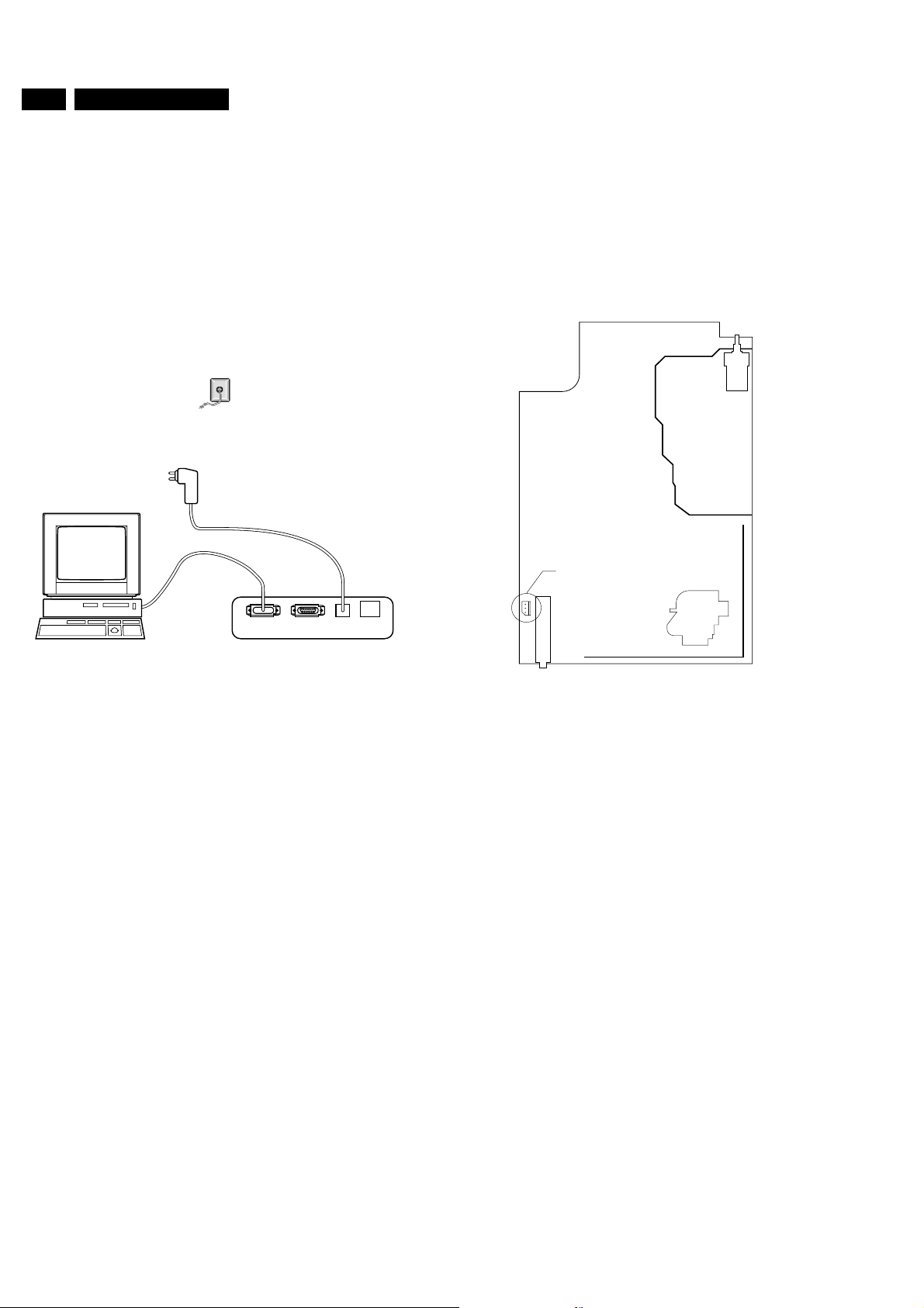
1. ConnecttheRS232interfacecable to a free serial (COMM)
port on the PC and the ComPair interface PC connector
(connector marked with "PC").
2. Place the ComPair interface box straight in front of the
television with the infrared window (marked "IR") directed
to the television LED. The distance between ComPair
interface and television should be between 0.3 and 0.6
meter. (Note: make sure that (also) in the service position,
the ComPair interface infra red window is pointed to the
standby LED of the television set (no objects should block
the infra red beam)
3. Connect the mains adapter to the connector marked "POWER 9V DC" on the ComPair interface
4. Switch the ComPair interface OFF
5. Switch the television set OFF with the mains switch
6. Remove the rear cover of the television set
7. Connect the interface cable (4822 727 21641) to the
connector on the rear side of the ComPair interface that is
marked "I2C" (See Figure 5.6)
Page 14
14 L9.1A
5 Fault finding and repair tips
8. Connect the other end of the interface cable to the
ComPair connector on the monocarrier (see figure 5.7)
9. Plug the mains adapter in the mains outlet and switch ON
the interface. The green and red LEDs light up together.
The red LED extinguishes after approx. 1 second (the
green LED remains lit).
10. Start-up ComPair and select "File" menu, "Open...:; select "L9.1A Fault finding" and click "OK"
11. Click on the > icon to switch ON the communication mode
(the red LED on the ComPair interface wil light up)
12. Switch on the television set with the mains switch
13. When the set is in standby. Click on "Start-up in ComPair
mode from standby" in the ComPair L9.1A fault finding
tree, otherwise continue.
Figure 5-5
• ComPair interface (excluding transformer): 4822 727 21631
• ComPair transformer (continental) Europe: 4822 727 21632
• ComPair transformer United Kingdom: 4822 727 21633
• Starterkit ComPair software: 4822 727 21634
• Starterkit SearchMan software: 4822 727 21635
• Starterkit ComPair+SearchMan software: 4822 727 21636
• ComPair CD (update): 4822 727 21637
• SearchMan CD (update): 4822 727 21638
• ComPair interface cable (for L9): 4822 727 21641
COMPAIR
PC VCR I2CPower
Figure 5-6
The set has now started up in ComPair mode. Follow the
instruction in the L9.1A fault finding tree to diagnose the set.
Note that the OSD works but that the actual user control is
disabled
5.8.3 Preset installation
Presets can be installed in 2 ways with the L9.1A.
• Via infra red
– only sending TO the television
– the rearcover does NOT have to be removed
Click on "File" "Open" and select "TV - use ComPair as DST" to use infra red
• Via cable
– sending TO the television and reading FROM the
television
– the rearcover has to be removed
Clickon "File" "Open" and select "L9.1A faultfinding" tousethe cable
9V DC
86532027_003.EPS
050898
0267
1
3
TUNER
CL 96532017_001.EPS
Figure 5-7
190299
Presets can be installed via menu "Tools", "Installation", "Presets".
5.9 Ordering ComPair
ComPair order codes:
• Starterkit ComPair+SearchMan software + ComPair interface (excluding transformer): 4822 727 21629
Page 15

8 Alignments
8 Alignments
General: the Service Default Mode (SDM) and Service Alignment Mode (SAM) are described in chapter 5.
8.1 Alignment conditions
All electrical adjustments should be performed under the following conditions:
• Supply voltage : 220V - 240V ( 10% ) for 230V sets and 100V - 110V ( 10% ) for 110V sets.
• Warm-up time: 10 minutes
• The voltages and oscillograms are measured in relation to the tuner earth.
• Test probe: Ri > 10MΩ Ci < 2,5 pF.
41L9.1A
• The VG2 adjustment has now been completed; Switch the
set to Standby. The values used for the BRIGHTNESSand the CONTRAST-during the alignment, will revert back
to their original values.
8.2.2 Focusing
Set the pattern generator (e.g. PM5418) so that the Circle and
Small Squares pattern is visible. Connect via the RF input with
an RF signal amplitude of 10mv. Adjust focus potentiometer
(positioned on the LOT 5445 ) for maximum sharpness of the
picture.
8.3 SOFTWARE ADJUSTMENT
8.1.1 Selection of the SDM-menu
– Bytransmitting the "DEFAULT" command with the RC7150
Dealer Service Tool (this works both while the set is in
normal operation mode or in the SAM)
– Standard RC sequence 062596 ( within OSD time-out )
MENU
– By connecting test-point M25 and M24 together on the
mono-carrier while switching on the set. After switching on
the set connection can be removed. ( Caution!! This also
overrides all the 5V protections .
8.1.2 Selection of the SAM-menu
– By transmitting the "ALIGN" command with the RC7150
Dealer Service Tool
– By pressing the "CHANNEL DOWN" and "VOLUME
DOWN" key on the local keyboard simultaneously when
the set is in SDM
– Standard RC sequence 062596 ( within OSD time-out )
OSD
– By connecting together test-points M28 and M29 on the
mono-carrier while switching on the set. After switching on
the set the short-circuit can be removed. ( Caution!!
Overrides 5V protections ).
8.2 Electrical Alignments
8.2.1 VG2
• Use a pattern generator to display a blank raster.
• Program the pattern generator with a frequency of 475.25 MHz for PAL/SECAM or 61.25 MHz for NTSC.
• Switch on the TV set.
• Select the SDM-MENU. The tuner is set to a frequency of
475.25 MHz for PAL/SECAM or 61.25 MHz for NTSC.
• Select the" SAM-MENU".
• Press the "MENU" key on the RC to leave the SAM-MENU
and go to the normal user menu ( "SAM" remains
displayed at the top of the screen). Select with the MENU
UP/DOWN command the sub-menu BRIGHTNESS.
Change the default value from 31 to 50 with the MENU
LEFT/RIGHT keys. Select the CONTRAST sub-menu and
change the value from 31 to 0.
• Leave the normal user menu to return to the SAM-MENU, by pressing the MENU key on the RC.
• Select sub-menu VSB and change thevalue from 0 to 1 by
pressing the MENU LEFT key. CAUTION!! Depending on
the position of the VG2 potentiometer, the raster will turn
completely black because the Vertical deflection stage has
been disabled.
• Adjust with VG2 potentiometer (located on the LOT 5445)
so that the blue line in the middle of the screen is only just
visible.
8.3.1 Geometry adjustments
• Set the pattern generator (e.g. PM5418) so that the Circle
and Small Squares pattern is visible. Use an R.F
frequency of 475.25 MHz for PAL/SECAMand connect the
generator to the RF input. Use a signal amplitude of 10mV, France select L'-signal.
• First enter the SDM mode to set the tuner at 475.25 MHz.
• Enter the SAM mode andthen select GEOMETRY with the
up/down keys buttons on the RC, the respective items can
now be selected. Use the left/right buttons to adjust the
selected items so that the correct the picture geometry is
achieved.
Vertical Amplitude and Position
• Select Vertical Slope "VSL"and shift the testpattern to the
top. The text VSL and its value should be above the upper
half of the screen
• Select Service Blanking "SBL" and set it to 1. The lower half of the picture will be blanked.
• Press the up button once to select Vertical Slope "VSL".
Now align "VSL" to start the blanking exactly at the
horizontal white line at the centre of the test circle. "VSL"
has the correct value now and should not be adjusted any
further.
• Press the down button once to select "SBL" and set it back to 0. The full picture now reappears.
• Now select Vertical Amplitude "VAM" and align the picture
height to the top of the screen, so that the top horizontal
linejust disappears. This corresponds with an overscan of
approx. 6%.
• Select Vertical Shift "VSH" and align for vertical centring of the picture on the screen.
• Repeat the last two steps if necessary.
Select Vertical S-correction "VSC" to align the top/bottom
squares till they have the same size as the squares in the
middle of the screen.
Page 16
42 L9.1A
8 Alignments
TV LOCK
INSTALLATION
BRIGHTNESS
COLOUR
CONTRAST
AKB
VSD
TUNER
WHITE TONE
GEOMETRY
AUDIO
MENU
llllll
llllll
llllll
......
......
......
SAM
31
31
31
SAMAAABBC X.Y
MENU
L90 BBC X.Y
TUNER
IF-PLL
IF-PLL POS
AFA
AFB
L90 BBC X.Y
SAM
SAM
64
192
1
1
SAM
A-FM
AT
STEREO
L90 BBC X.Y
SOUND
SAM
232
15
MENU
MENU
NORMAL RED
40
SAM
L90 BBC X.Y
4
MENU
VAM
55
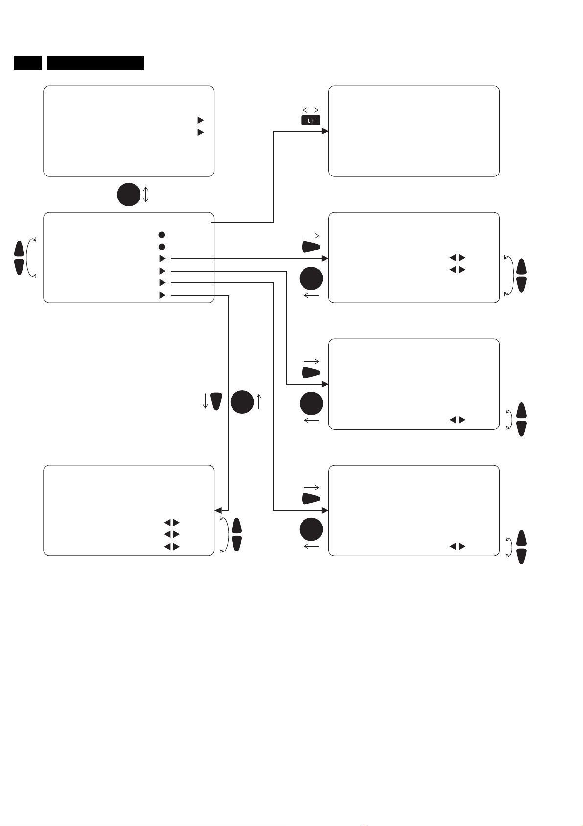
Figure 8-1 : Service Alignment Mode screens and
structure
CL 86532104_016.eps
030399
Page 17
8 Alignments
43L9.1A
Horizontal Amplitude and Phase
• Select Horizontal Shift "HSH" to horizontally centre the picture on the screen
For sets with E/W correction follow the instructions below:
• Select East-West Width "EWW" and align the picture with substantial over scan.
• Select East-West Trapezium "EWT" and align for a rectangle if necessary
• Select East-West Parabola "EWP" and align for straight vertical lines.
• Select East-West Corner "EWC" and align the corners.
• Repeat if necessary.
• Option code "H60" and "V60" do not need any alignment. Default value H60 and V60 = 10.
To return to the main SAM-menu , press the MENU key on the RC.
To exit the SAM-menu and store the alignments in the NVM, press the STANDBY-key on the RC.
8.3.2 AGC
Set pattern generator (e.g. PM5418) with colour bar pattern
and connect to aerial input with RF signal amplitude - 10mV
and set frequency for PAL/SECAM to 475.25 MHz. For France
select the L'-signal.
• Select the" SAM-MENU".
• Select the TUNER sub-menu and select the AFW option. Set this to a value of 80kHz.
• Select the AGC subsub-menu
• Connect a DC multi-meter to pin 1 of the tuner IC 1000.
• Adjusting the AGC until the voltage at pin 1 of the tuner is
1.0V +/- 0.1V.
• The value can be incremented or decremented by pressing the right/left MENU-button on the RC.
• Switch the set to standby.
8.3.5 White tone
• Connect a pattern generator (e.g. PM5418) and set it to colour bar and circle pattern.
• Set the frequency and output for PAL 475.25MHz with RF
signal amplitude of 10mv and connectto tuner (aerial) input
• Enter the SAM -MENU.
• Enter the WHITE TONE menu and then select either
NORMAL, DELTAWARM, or DELTACOOL depending on
the item which needs to be aligned. Only one of the three
items (R, G or B) will be displayed on the screen.
The default values for the colour temperature as displayed in the table below:
NORMAL 10500K R = 40 G = 40 B = 40 (DELTA)COOL 14000K R = -2 G = 0 B = 6 (DELTA)WARM 8200K R = 2 G = 0 B = -7
Switch the set to standby.
8.3.6 Audio
NO ADJUSTMENTS NEEDED FOR SOUND.
The default values for the audio alignments, with option code
ND for the soundboard option "SB" - the most extended
version, are displayed in the table below:
AUDIO Alignment Options
A-FM 232
AT 4
STEREO 15
8.3.3 IF-PLL
Connect a pattern generator (e.g. PM5418) and select colour
bar pattern and connect to the aerial input with RF signal
amplitude of 10mV and set frequency to 475.25 MHz for PAL/
SECAM or 61.25 MHz for NTSC.
• Select the " SAM-MENU".
• Select at the TUNER sub-menu and set the AFW at its lowest value.
For the IF-PLL option the following should be done:
• Select at the TUNER menu the IF-PLL subsubmenu
• Adjust the IF-PLL value until AFA becomes "1" and AFB alternates between "0" and "1"
• Switch the set to Standby.
8.3.4 Tuner options CL and YD
NO ADJUSTMENTS NEEDED FOR THESE ALIGNMENTS. The default values for these option codes are:
– CL : 4
– YD : 12
DUAL 15
The presence of an item in the menu is dependent on the selected soundboard (option SB).
8.4 Options
Options are used to control the presence / absence of certain
features and hardware. There are two ways to change the
option settings. The various option configurations and the
descriptions of the two character-codes are explained below.
Changing a single option:
A single option can be selected with the MENU UP/DOWN
keys and its setting can be changed with the MENU LEFT/
RIGHT keys.
Changing multiple options by changing option byte values:
Option bytes make it possible to align very all the options. An
optionbyte represents a number of different options. All options
applicableto the L9 are controlled via 7optionbytes. Select the
option byte (OB1, OB2, OB3, OB4, OB5,OB6 or OB7) and key
in the new value.
Changes in the options and option bytes settings are saved
when the set is switched to standby. Some changes will only
Page 18
44 L9.1A
8 Alignments
take affect after the set has been switched OFF and ON with
the mains switch (cold start).
The following options in SDM can be identified:
OP OPTION (ON=enabled / present). Explanation /
Remark
AC Alternate Channel. Alternate channel function
(SWAP between last presets) enabled
AM Animated Menu
2X External 2AS. Autostart up/Micro controller start up
Default value is On (ON = start up via micro
controller, OFF = auto start up BIMOS
BM Blue mute (ON = enabled). Enabled: blue mute
background in case of no video ident/poor signal
conditionsBSBIMOS standby mode Default value =
ON
BL Balance . Enabled: menu item BALANCE available
BT Bass/Treble Control. Menu controls for BASS and
TREBLE available when enabled
CH Child lock. Menu item Child lock when enabled
CK Clock (Volatile). Clock function available when
enabled
CL Child Lock. Menu item Child Lock/Parental control
when enabled
CP Contrast Plus. Menu item Contrast Plus available
when enabled
CX 16:9 Compress. Menu item 16:9 compress when
enabled
DM Demo Mode Demonstration of TV functions on
screen when enabled
DU Dual I/II. Possibility of language selection when
enabled
EW East-West Control. East-West Alignment in SAM
GEOMETRY menu available when enabled
EX 4:3 Expand. 4:3 expand mode available when
enabled
FQ Frequency display. Frequency displayed when
enabled
HS Hospital Mode. Possibilityto block the local keyboard
when enabled
IS Incredible Surround. Incredible surround function
available when enabled
MS Message . Menu item Message when enabled
NI NoIdent Auto Standby .Setswitches to standby after
10min. when NI enabled
NR Noise Reduction . Menu item Noise Reduction when
enabled
SA Spatial (Incredible stereo). Menu item Incredible
Stereo when enabled
SB Sound Board (Set the sound hardware configuration)
MA = Mono All
60= Mono All with stereo playback
MM= Multi Mono
IT = 2CS stereo processor MSP3400 (German or
Korean stereo)
NB = Nicam/2CS processor MSP3410B
ND = Nicam/2CS processor MSP3410D
SP SmartPicture. Smart picture command is processed
when enabled
SS Smart Sound. Smart sound command is processed
when enabled
ST Sound systems supported
SS = BG, I, DK, M
AD = BG/I, BG/DK, I/DK
SY Systems supported
SS = Single system
AD = AP Dual
AM = AP-Multi
AF = AP-Full Multi
TN Tuner (OFF: Philips tuner, ON: ALPS tuner) Default
value = OFF
TW Channel Select Time Window (OFF: 2 seconds, ON:
5 seconds) Time interval for entering a second digit
for channel selection
UB Ultra Bass. Ultra bass function available when
enabled
VI Virgin ModeOSD at very first installation when
enabled
(*)Remark: When the option RC= OFF, the P+ and the P- key
on the remote control have the same functions as the MENU
UP/DOWN keys while the VOL+ and the VOL- key have the
same function as the MENU LEFT/RIGHT keys. When
RC=OFF, it is not possible to change the channel pre set or to
adjust the volume in SAM/SDM with the remote control.
RC = OFF for use with L7-based remote control (only cursor
keys). RC = ON for use with A8-based remote control (cursor
keys, P+/P- and Volume+/Volume-).
8.5 Option bits/bytes
OB1 bits 8, 7, ..., 1: DP, FQ, AM, HS, HT, DM, GM, VI
OB2 bits 8, 7, ..., 1: CK, CL, AT, CI, FV, HC, SS, SP
RC (*) Separate preset/volume control on remote control
(ON = separate control (A8 RC); OFF = combined
control (L7 RC))See note below table. Default value
is OFF
OB3 bits 8, 7, ..., 1: RC, CH, (res), (res), TW, AC, SF, VM
OB4 bits 8, 7, ..., 1: TN, FT, XT, 2X, XS, CD, BM, NI
OB5 bits 8, 7, ..., 1: EX, CX, NR, CP, CT, EW, BS, AS
Page 19

8 Alignments
OB6 bits 8, 7, ..., 1: BT, IS, VL, DV, UB, LV, DU, AO
OB7 bits 8, 7, ..., 1: ST, ST, SB, SB, SB, SY, SY, SY
An option byte value is calculated in the following way:
value "option bit 1" x 1 =
value "option bit 2" x 2 =
value "option bit 3" x 4 =
value "option bit 4" x 8 =
value "option bit 5" x 16 =
value "option bit 6" x 32 =
value "option bit 7" x 64 =
value "option bit 8" x 128 =
Total : value "option byte" =
45L9.1A
Page 20

46 L9.1A
9 Circuit description new circuits
Power supply (diagram A1)
9 Circuit description new circuits
9.1 Introduction
9.1.1 General
The switch mode power supply (SMPS) is mains isolated. The
control IC7520 (MC44603A) produces pulses for driving FET
7518. Power supply regulation is achieved by using duty cycle
control at a fixed frequency of nominal 40 kHz in normal
operation. In stand-by, slow-start and overload situations the
SMPS runs at frequencies other than 40 kHz.
Basic characteristics of this SMPS :
– Mains Isolated flyback Converter type
– Input range : 90 - 276 Volts AC
– Secondary Sensing by Opto-coupler
– IC7520 is Featured with Slow-Start circuitry
– Protection Circuits
– Degaussing circuit
9.1.2 Output voltages
• Audio Supply ( +16.5V ) for the AUDIO AMPLIFIER ( Diagram A12 )
• Mains Supply ( +140V ) for the HORIZONTAL DEFLECTION stage (A2) and the CRT discharge circuit (A3)
• Vaux ( +11.3V ) for the Video IF (A5), Video processing (A6) and Control circuit (A7)
9.1.3 The switching periods of TS7518
The power supply duty cycle is dependent on the T-on of FET
7518.The FET is driven by pin 3of IC7520.ThisIC controls the
secondary voltage (VBATT via opto-coupler 7581 and
regulator 7570. The switching period of TS7518 can be divided
into three main phases: Duty cycle T-on, T-off and T-dead.
• During T-on, FET 7518 conducts.
• Energyis stored in the primarywinding (2-5)of transformer
T5545 by using a linear increasing primary current. The
slope depends on the rectified mains-voltage present
across C2508. The T-on period is varied to provide
regulation of the drive waveform at pin 3 of IC7520. By
controlling the duty cycle of the SMPS in this way the
(VBATT is controlled.
• During T-off, FET 7518 is switched off and therefore does
not conduct. The energy is now transferred to the
secondary side of the transformer and then supplied to the
load via the secondary diodes (D6550, D6560 and
D6570,D6590). The current through the secondary side of
the transformer decreases until it reaches zero.
• During T-dead FET 7518 does not conduct .The voltage at
the drain of the FET decays and eventually reaches the
input voltage of approximately 300V.
9.2 Primary side
9.2.1 Mains input and degaussing
initial power on. The PTC will then heat up due to the high
current involved and becomes high-ohmic which reduces
the degaussing-current. During normal operation, the
degaussing current is zero, because relay 1580 is open
due to the absence of the (P - Reset signal.
9.2.2 Start up and take over
– Start-up : The start-up circuitry consisting of 3510, 3530
and 3529 use the voltage coming from the 230V AC mains
to start-up IC7520 via the supply pin 1. The output drive
waveform (pin 3) is blocked by using the ICs internal logic
until the voltage on pin 1 reaches 14.5 Volts however with
less than 14.5 volts on Pin 1 the IC only consumes 0.3mA.
Once pin 1 reaches the 14.5 Volts threshold, IC7520 will
start up (FET 7518 will conduct) and pin 1 sinks a typical
supply current of about 17 mA. This supply current cannot
be delivered by the start-up circuitry, so a take-over circuit
must be present. If take-over does not occur then the
voltage on pin 1 will decrease below 9V and IC7520 will
switch off. The supply begins a new Start-up cycle, seetop
of this paragraph. This cycle will repeat itself and can be
noticed by an audible hick-up sounding noise.
– Take for IC7520: During start-up a voltage across winding
8- 9 is gradually builtup. At the moment thevoltage across
winding 8 - 9 reaches approx. (14.5 Volts, D6540 start
conducting and takes over the supply voltage Vpin 1 of
IC7520 (take over current is approx. 17mA).
Note: This power supply is a SMPS (= Switched Mode Power
Supply) and not a SOPS (= Self Oscillating Power Supply).
9.3 Control circuitry
9.3.1 IC7520 control mechanisms
IC7520 controls the T-on time of FET 7518 in four different ways:
• "Secondary-output-sensing"controls the secondary output voltages via the feedback voltage pin 14
• "Primary current sensing" control due to the mains voltage via the current sense voltage pin 7
• "Demagnetization control" prevents the transformer T5545
from going into saturation via the so-called "DEMAG"
function at pin 8
• Mains voltage control via R3514 and R3516
9.3.2 Secondary voltage sensing (pin 14 of IC7520)
When the output voltage +VBATT increases (due to a
reduction in the load ) the current through the led in the optocoupler 7581 will increase due to the fact that the seriesresistor in regulator 7570 decreases. An increase in optocoupler led-current (7581) results in a decrease in the Vce of
transistor 7581, therefore the voltage across capacitor 2576
increases. This will reduce the on-time of FET 7518 due to an
increase of the voltage present on pin 14.
In the event of an increase of the load (decrease of output
voltage +VBATT ), the control circuit will work in the opposite
way to the explanation above.
– Mains voltage: this voltage is filtered by L5500 and L5502,
rectified by a diode bridge rectifier 6505 and then
smoothed by C2508 which provides a DC input voltage of
300V DC for an ac input voltage of 230V.
– Degaussing : R3503 is a PTC. When switching "on" the
set,thePTCiscold and has a low-ohmic value. Relay 1580
is activated while the Reset signal, coming from the (P is
present. This allows a very high degaussing current at
9.3.3 Primary sensing (pin 7 of IC7520)
The current sense voltage at pin 7 is used to measure the
primary current through FET7518. The primary current is
converted into a voltage by R3518. R3514. 3516. couples a
partof the main voltage to the samepin7 of IC 7520 by dividing
this sample of the voltage.
Page 21
9 Circuit description new circuits
47L9.1A
Hencethehighertheinputvoltagethemoretheprimarycurrent
is limited. In this way the maximum output power of the powersupply is limited.
9.3.4 Demagnetization control (pin 8 of IC7520)
Winding 8 - 9 has the same polarity as the secondary winding
that supplies the load. WhenFET 7518 is turned offthe voltage
at winding 9 becomes positive. The power supply transfers the
stored energy at the secondary side. Until the transformer is
demagnetized the voltage on the winding remains positive. At
the moment that the energy is fully transferred to the load, the
voltage at pin 9 of the transformer becomes negative.
Additionally with a certain dead time the voltage at control pin
8 of IC 7520 also drops below zero which releases the output
buffer (pin 3) and a new cycle starts.
9.3.5 Peak current limiting
An internal clamp at pin 7 allows peak current limiting to be
achieved . This pin can never exceed 1V DC and so the
maximum primary current through FET 7518, and also the
maximum output power is determined. In case of an output
being short-circuited or loaded excessively, the I-prim
becomes too high which is detected by pin 7. As a result the
primary current is limited to its maximum value and the
secondary voltages will drop. The voltage at pin 1, which is
coupled with the output voltage, will also drop. When the
voltage at pin 1 drops below the 9V, IC7520 will stop
functioning and the output voltage will rapidly drop to zero.
Via start-up circuitry 3510, 3530 and 3529 the voltage
originating from the 230V AC mains is used to start-up IC7520
viathe supply pin 1. Assoon as this voltage reachesthe 14.5V,
IC7520 starts functioning. If the load is still too much or the
output is short-circuited the same cycle willhappen again. This
fault condition can be clearly identified as the power supply will
be loudly tripping.
9.3.6 Slow-start
As soon as Vpin 1 > 14.5V the SMPS will start-up. During the
slow-start procedure both the frequency and the duty cycle will
be built up slowly. The duty cycle will initially slowly increase
commencing with the absolute lowest possible duty cycle. The
maximum duty cycle is determined by C2530 at pin 11 of
IC7520, as C2530 is uncharged at start-up.
9.3.7 Standby mode
In standby mode the SMPS switches to the so-called "reduced
frequencymode" and runs at about20 kHz. During standby the
SMPS only has to deliver a minimal level of output power. The
minimal load threshold level is determined by R3532 at pin 12.
In the L9 chassis the SMPS does not have a burst mode in
standbybut only a reduced frequency mode ofabout20 kHz as
stated above. In normal operation mode the internal oscillator
is around 40 kHz. This frequency is controlled by C2531 at pin
10 of IC7520 and by R3537 at pin 16 of IC7520. In standby
modethe frequency of operation isdetermined byR3536 at pin
15 of IC7520.
9.3.8 Protections
Over voltage protection of the secondary voltages.
After start-up the supply voltage pin 1 will be "taken over" by
winding8 - 9. Pin1 of IC 7520 isused to detect an over voltage
situation on the secondary side of the transformer. If this
voltage exceeds 17V (typically the output buffer is disabled,
and IC 7520 goes into over voltage protection and a complete
restart sequence is required. Check in this case IC7520,
IC7581 and the secondary voltage +VBATT ( +140V ).
REMARK: In the event of the over voltage situation remaining
present, the SMPS will go in protection, start up cycle,
protection, etc. The standby led on the front of the set starts
flashing.
Under voltage protection of the secondary voltages
If the supply voltage at pin 1 of IC 7520 drops below 9V
because of a short-circuit or excessive load, the drive pulse
present at pin 3 will be disabled and IC7520 will switch off the
complete SMPS. Capacitor C2450 is charged up via start-up
resistors 3510, 3530 and 3529, however once the voltage
exceeds 14.5V start up threshold, the SMPS will once again
commence a re start cycle.
Intheeventof the under voltage situation remaining, the SMPS
will again go in protection mode, startup cycle, protection, etc.
and so the cycle repeats. This effect is highly audible.
9.4 Audio processing
The following systems are available:
• BASIC : MONO/AV STEREO ( M,BG, I and DK : single or dual system )
• NICAM: FM STEREO / NICAM L/L',NICAM I, NICAM B/G, NICAM DK
• 2CS: FM STEREO / FM MONO ( allstandards4.5, 5.5, 6.5 MHz )
• BTSC : MONO/STEREO/STEREO-AP
MONO/AV STEREO, BTSC DBX incorporating 2CS (two
carrierstereo) use a TDA8844/43 BIMOS device(built-in Mono
FM Demodulator circuit).
NICAMLL',/BG, /I versions use a TDA8845 BIMOS (AMsound demodulator & QSS-IF circuit ; built-in)
The Audio Module incorporates for each system a different multi digital sound processor.
• MONO /AV STEREO: BSP3501 & TDA884x
• NICAM / 2CS : MSP3415D
• BTSC : MSP3535G
These IC's have an incorporate digital audio processing for
volume, bass, treble, balance, mute, spatial sound, incredible
sound, smart sound andsource selection (SIF-signal, EXT1 or
EXT2).
9.4.1 MONO / AV STEREO
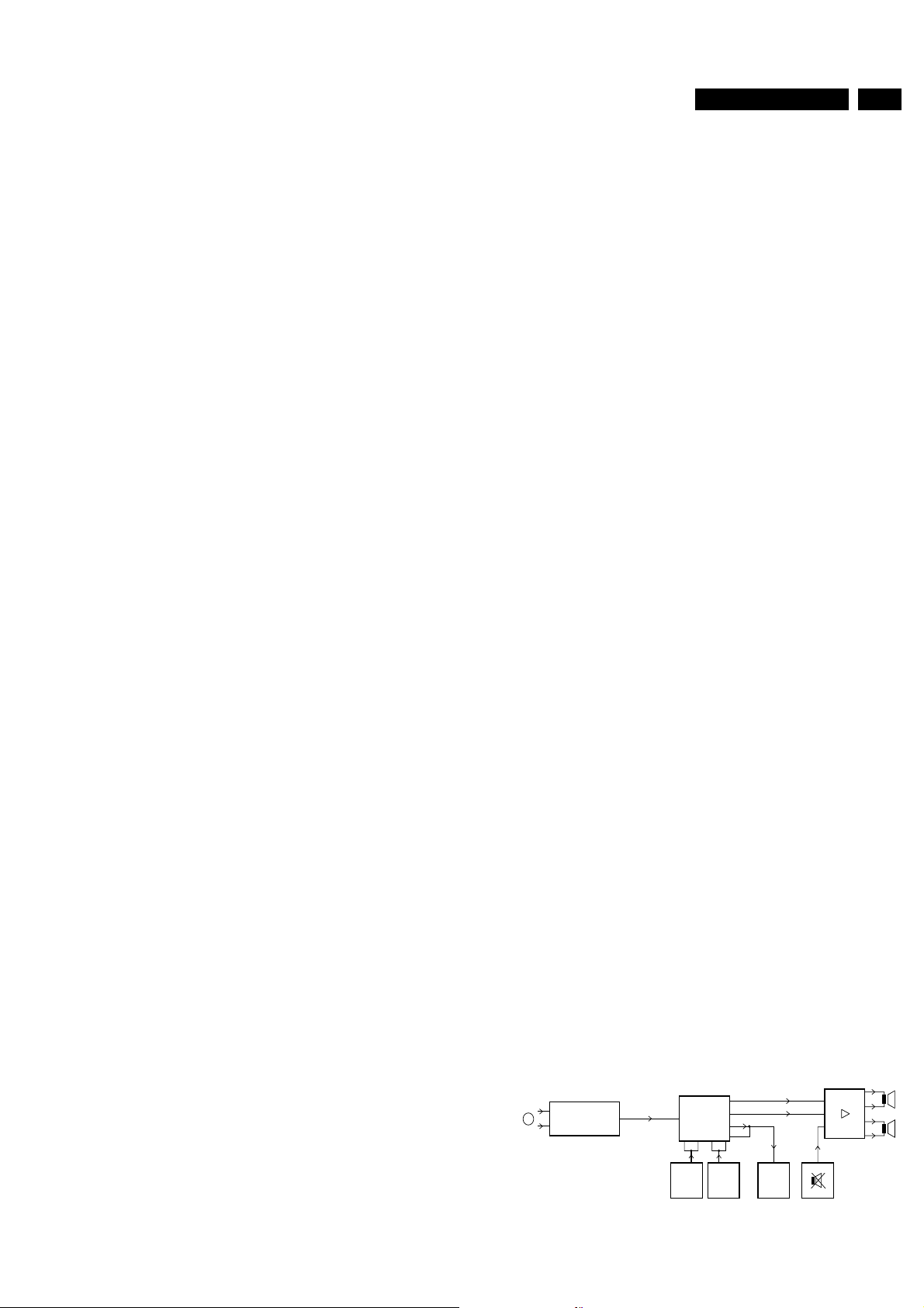
This set does have the digital sound processor BSP3501, IC7833.
MONO/AV STEREO
7250-A
48
IF
TDA 8844
49
15
AUDIO OUT
7833
58
BSP3501
52 53 49 50
EXT. 1
AUDIO
EXT. 2
AUDIO
28
29
36
37
LEFT OUT
RIGHT OUT
REAR
Figure 9-1: "MONO / AV STEREO SETS"
7952/7951
3
5
CL 86532104_068.eps
8
10
11
13
+
R
-
R
-
L
+
L
290399
Page 22
48 L9.1A
9 Circuit description new circuits
The video IF output is present at pin 11 of the tuner 1000. This
signalgoes through a sound SAW filter and isfed tothe BIMOS
via pins 48 and 49, where the signal is demodulated. . At pin 6
of BIMOS IC 7250-A, the CVBS + SIF signal is fed to another
SAW filter. Signal P3Duall/Mono selects either SAW filter 1001
or SAW filter 1002.
The system hardware configuration, option code SY, is set at
AD - Dual Mono for a Dual configuration, while option code SY
is set at SS for the Mono configuration ( BG,I, DK, M ). Via
P3Duall/Mono, a signal coming from the Micro-processor
IC7600, it possible to switch between two Mono configurations
(BG/DK or BG/I or DK/I).
This signal goes back to pin 1 of the BIMOS , for further
demodulation. The demodulated FM signal or the REAR I/O
audiosignal,ExtAudioMonoatpin 2, is switched by the BIMOS
and is present at pin 15.
The signal at pin 15 is fed to pin 55 of IC 7833 - BSP3501C - at
panel A10 . IC 7833performs source selection as well as audio
processing such as volume, bas, treble, balance, tone control
and spatial stereo. The audio output from IC 7833, pin 28 and
pin 29, is fed to the power amplifier IC 7950 or IC7951. Pin 36
and 37 pass the same selected signal through to the Audiocinches.
Signal P10MuteVolume enables the output of the sound amplifier.
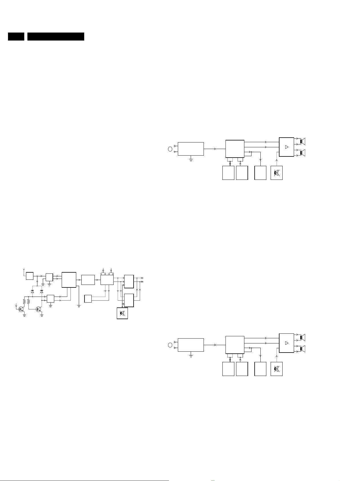
9.4.2 NICAM
Thishigh quality digital audio formatis usedin Eastern Europe,
France, and UK, while NICAM LL' is being used in France. The
figure below shows the AUDIO path for NICAM..
P2LLP/MTRAP
1000
11
7701 7702
1
1003
2
124
1204
NICAM
7250-A
4548
VIF
49
3
5
3
258
TDA 8845
15
55 56
FILTER
SELECTION
REAR
EXT 1
AUDIO
52
MSP 3415
53
36 37
EXT 2
AUDIO
49
7833
9.4.3 2CS
This analogue F.M stereo audio standard is predominately
used in Germany and The Netherlands. It is used on some
cable television networks. The diagram below indicates the
AUDIO path for 2CS.
The CVBS + SIF signals present at pin 6 from BIMOS, TDA8844-, are passed through a high pass filter and are then
fed back into pin 58 of IC 7833 (MSP3415D) for further
demodulation. All variants of 2CS are demodulated in this IC.
2CS
7952/7951
3
5
7250-A
48
IF
TDA 8844
49
6
15
(CVBS+SIF)
7833
58
MSP3415
52 53 49 50
EXT. 1
AUDIO
EXT. 2
AUDIO
28
29
36
37
LEFT OUT
RIGHT OUT
REAR
+
R
8
-
R
10
-
L
11
+
L
13
CL 86532104_071.eps
300399
Figure 9-3: "2CS"
Audio signals coming from the rear I/O panel are connected to
pin 49/50 of IC7833 for the Ext1Audio signals, while pin 52/53
of IC 7833 are used for the Ext2Audio signals. IC 7833
performs source selection as well as audio processing such as
volume, balance, tone control, mute, spatial stereo, incredible
surround sound and SMART sound. The audio output from IC
7833, pin 28 and pin 29, is fed to the power amplifier IC 7950
or IC7951. Pin 36 and 37 pass the same selected signal
through to the audio-cinches. Signal P10MuteVolume enables
the output of the sound amplifier.
7950
50
R-OUT
28
L-OUT
29
TDA 7057
7951
TDA 7053
-
L+/L
-
R+/R
9.4.4 BTSC DBX
The CVBS + SIF signals from the BIMOS are passed through
a high pass filter and are then fed back into pin 58 of IC 7833
(MSP3435G)for further demodulation. This signalis present at
pin 2 of BIMOS -TDA8845- for NICAML and present at pin 6 of
BIMOS - TDA8844 - for all other NICAM/2CS applications.
CL 86532104_010.eps
080299
Figure 9-2: "NICAM"
The video IF output is present at pin 11 of the tuner. Signal
P2LlpMono is used to switch between NICAM L or L'.
Depending on the required Tuner frequency band, the
appropriate SAW filter is selected. The filtered signal is fed to
SIF (sound I.F amplifier) input pin 55 and 56 of the BIMOS TDA8845. Output pin 15 - AM Audio output-, is connected to
ground via jumper 4002.
The QSS signal at pin 2 passes throughthe selected high pass
filter, depending on the system used, and is fed to sound
processor 7833. Audio signals coming from the rear I/O panel
areconnectedtopin 49/50 of IC7833 for the Ext1Audio signals,
while pin 52/53 of IC 7833 are used for the Ext2 Audio signals.
The QSS-signal, Ext1Audio or Ext2Audio is switchedinternally
tothe output pins 28 and 29of the sound processor. Pin 36and
37 pass the same selected signal throughto the audio-cinches.
The audio output of the MSP3415 is fed to the power amplifier
IC 7950 or IC7951. Signal P10MuteVolume enablesthe output
of the sound amplifier.
BTSC DBX
7250-A
48
IF
TDA 8844
49
6
15
(CVBS+SIF)
7833
58
MSP3435
52 53 49 50
EXT. 1
AUDIO
EXT. 2
AUDIO
28
29
36
37
LEFT OUT
RIGHT OUT
REAR
Figure 9-4: "BTSC DBX"
Audio signals coming from the rear I/O panel are connected to
pin 49/50 of IC7833 for the Ext1Audio signals, while pin 52/53
of IC 7833 are used for the Ext2Audio signals. IC 7833
performs source selection as well as audio processing such as
volume, balance, tone control, mute, spatial stereo, incredible
surround sound and SMART sound. The audio output from IC
7833, pin 28 and pin 29, is fed to the power amplifier IC 7950
or IC7951. Pin 36 and 37 pass the same selected signal
through to the audio-cinches. Signal P10MuteVolume enables
the output of the sound amplifier.
7952/7951
3
5
CL 86532104_067.eps
8
10
11
13
+
R
-
R
-
L
+
L
290399
Page 23
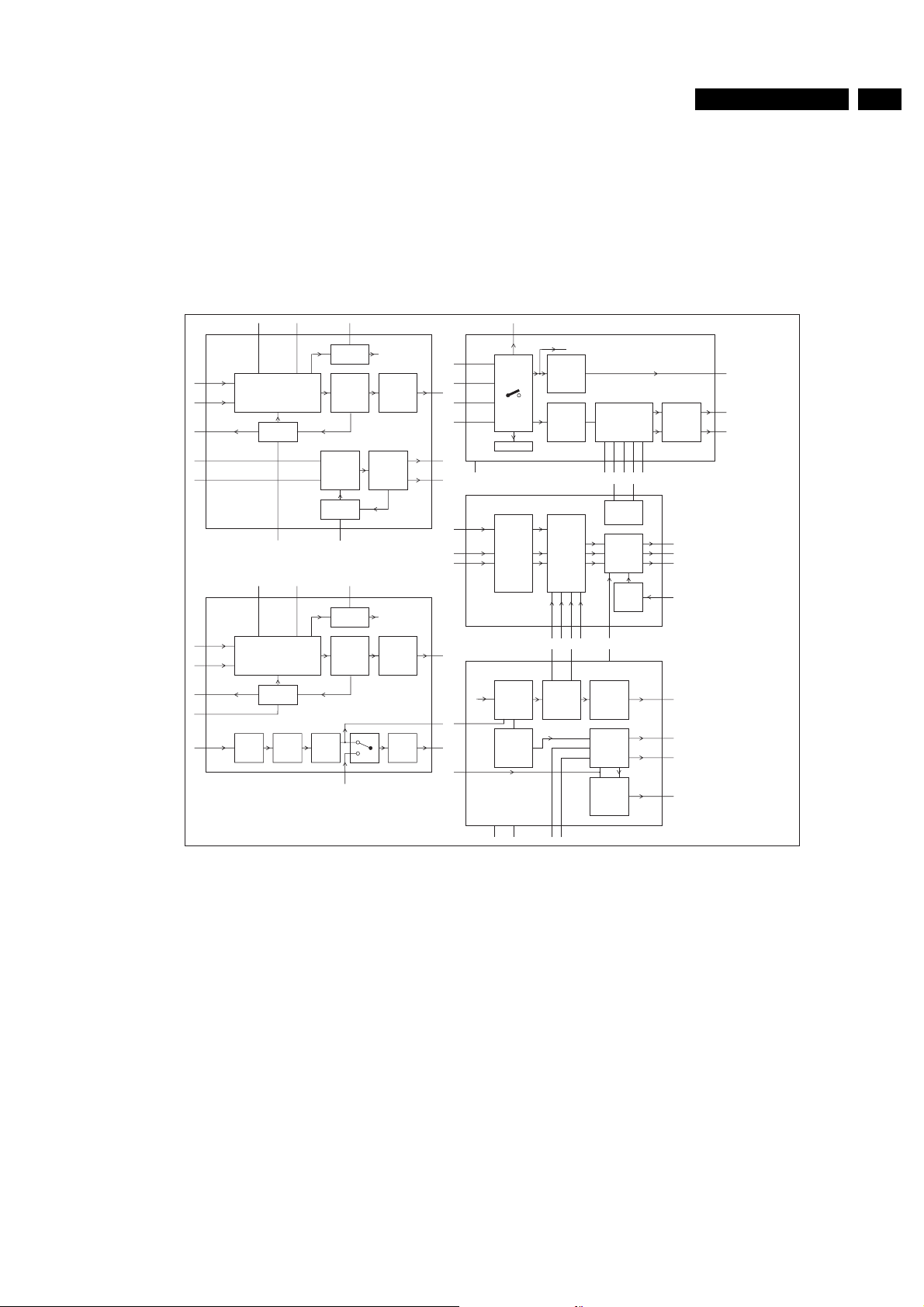
9 Circuit description new circuits
49L9.1A
9.5 Tuner and Video IF (see circuit diagram A5)
9.5.1 Introduction:
In Figure 9.4 a simplified block diagram of the video path is
shown. The main item in the block diagram shown in Fig.9.5 is
the video processor item 7250. The IC performs the following
functions,video IF demodulation, chroma processing and RGB
processing. Additionally synchronisation processing, mono IF
audio demodulation and audio selection takes place.
IC 7250-4A
TDA 8845
48
49
54
55
56 15
IC 7250-4A
TDA 8844
48
49
54
53
1
34 5
IF AMPLIFIER
+
PLL VIDEO DEMO.
AGC
SOUND
IF
AMPL.
AGC
53
OR
34 5
IF AMPLIFIER
+
PLL VIDEO DEMO
AGC
PLL-
AUDIO
FM DEMO.
AMPL.
MUTE
+
LIMITER
AFC
VIDEO
AMPL.
1
AFC
VIDEO
AMPL.
2
AFC
VIDEO-
BASEBAND
OUTPUT
QSS MIXER
+
SOUND
AM DEM.
AFC
VIDEO-
BASEBAND
OUTPUT
OUTPUT
VOLUME
CONTROL
+
6
2
6
55
15
7250-4B
TDA 8844/45
13
17
10
11
7250-4C
TDA 8844/45
27
Y
31
U
32
V
7250-4D
TDA 8844/45
Y
43
50
38
VIDEO IDENT
CD MATRIX
+
SATURATION
CONTROL
+
SKIN
TINT
SYNC.
SEPARATOR
VERT.
SYNC.
SEPARATOR
Two versions of video processors are used:
• TDA8844 N2 for SW CENELEC BG/DK, CENELEC I NICAM, CENELEC BG NICAM
• TDA8845 N1 for CENELEC BG,LL',I
For a detailed block diagram of the TDA8844/8845 see Figure
9.5.
Y (TO SYNC PART)
LUM.
DELAY
PEAKING
CORING
CHROMA
BANDPASS
RGB
MATRIX
+
BLACK
STRETCH
+
RGB1
INPUT
41 42 37
VCO
HORIZONTAL
+
CONTROL
52514439
PAL/NTSC/
SECAM
DEMODULATOR
169 36353433
78
IIC BUS
CONTROL
R
RGB
G
OUTPUT
B
CATH.
CALIB.
2223 24 25 26
OUTPUT
VERTICAL
OUTPUT
E/W
OUTPUT
21
R
20
G
19
B
18
40
46
47
45
BASE-
BAND
DELAY
LINE
RGB
OUTPUT
SYNC
28
INPUT SELECT
Y + CHROMA
29
PROCESSING
30
CL 86532104_021.EPS
220299
Figure 9-5 :Bimos
9.5.2 Tuner
The PLL tuner (item 1000) is digitally controlled via the I2Cbus.The tuner is suitable toreceive off-air,S-(cable) and hyper
band channels.
Tuner pin description:
• Pin 1: AGC, Automatic gain control voltage input (0.3 -
4.0V)
• Pin 2: VT, tuning voltage input (not connected)
• Pin 3: AS, address select (not connected)
• Pin 4: SCL, IIC-bus serial clock
• Pin 5: SDA, IIC-bus serial data
• Pin 6: not connected
• Pin 7: Vs, PLL supply voltage +5V
• Pin 8: not connected
• Pin 9: Vst, tuning voltage +33V
• Pin 10: ground
• Pin 11: IF, asymmetrical IF output
Note: The +5V supply voltage and the +33V tuning voltage is
derived from the line output stage, see diagram A2).
9.5.3 IF band pass filter (SAW FILTER)
Between the tuner output and the video IF input of the video
processor the IF band pass filtering take place. Filter 5002 is
tuned at 40.4MHz and serves as an extra suppression of the
neighbour channel. For the IF band pass filtering SAW filters
are used (item 1003 or 1004). 5 Types of SAW filters are used
depending of the version of the set.
9.5.4 Video IF
General: Video IF-demodulation is achieved in combination
with reference circuit L5006 connected at pin 3 and 4 of
IC7250-A. The AGC control for the tuner is applied via pin 54
of IC7250-A. Internally the IC uses the top sync level as a
reference for AGC control. The AGC adjustment can be
readjusted via the SAM (service alignment menu). C2201
connected to pin 53 determines the time constant of the AGC.
The Base band CVBS signal is present at pin 6 of IC7250-A
(normal amplitude 3.2Vpp). From here the signal is fed via
Page 24
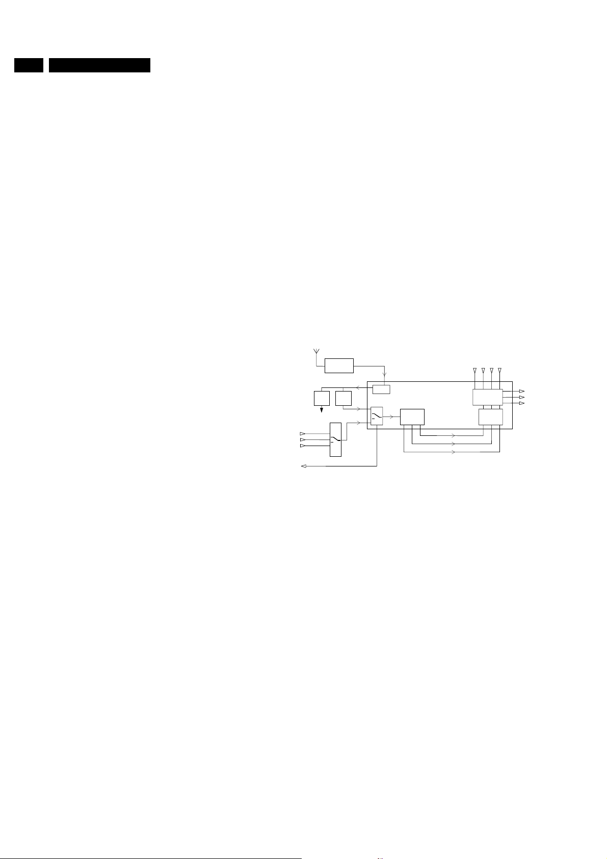
50 L9.1A
9 Circuit description new circuits
transistor7266tothesoundtrap filters and then on to the video
source selection circuit.
The main functions of the video IF partare (see also figure 9.5):
• IF- amplifier
• PLL-demodulator
• Video buffer
• AFC
• IF-AGC
• Tuner AGC
9.5.5 IF- amplifier
The IF-amplifier incorporates symmetrical inputs (pins 48 and
49). By using IIC bus control (IFS) the AGC attenuation can be
adjusted by up to -20db.
Remark: If the BIMOS is replaced the AGC value should be
adjusted as part of the repairprocess. (see software alignment
adjustments).
9.5.6 PLL-demodulator
The IF-signal is demodulated with the assistance of the PLL
detector. The video IF-demodulator can handle both negative
and positively modulated IF signals; selection is achieved via
the IIC bus (bit MOD).
9.5.7 Video buffer
The video buffer is present to provide a lowohmic video output
with the required signal amplitude. Additionally, it provides
protection against (pin 6) the occurrence of noise peaks. The
video buffer stage also contains a level shifterand a gain stage
for both the positive and negative video modulation formats, so
that the correct video amplitude and DC level are always
present at pin 6 regardless of the input signal.
9.5.8 Video-IF AGC
An AGC system controls the gain of the IF amplifier such that
thevideo output amplitude is constant.The demodulated video
signal is supplied, via a low pass filter inside the IC to an AGC
detector. External AGC de coupling is provided by capacitor
2201 at pin 53. The AGC detector voltage directly controls the
IF amplification stages.
9.5.9 The tuner AGC
Tuner AGC is provided to reduce the tuner gain and thus the
tuner output voltage when receiving to strong RF signal. The
tuner AGC starts working when the video-IF input reaches a
certain input level. This level can be adjusted via the IIC bus.
The tuner AGC signal is applied to the tuner via the open
collector output pin 54 of the BIMOS.
9.5.10 AFC
The AFC output information is available for search tuning. The
AFCoutputisavailable via the I2C bus ( AFA and AFB signals).
For alignment purposes it is displayed in the TUNER submenu
of the SAM (See chapter 8).
9.6 Video Signal Processing (see circuit diagram A6)
9.6.1 Introduction:
The video signal processing can be divided in the following parts:
• CVBS/Y/C input selection
• Luminance and chrominance signal processing
• PAL/NTSC and SECAM demodulation /Auto system manager
• YUV/RGB processing/ black stretcher
• Second RGB insertion
• RGB processing
• Black current calibration loop
• Beaming current limiting
Above mentioned processing circuits are integrated in the TVprocessor (parts B and C). The surrounding components are
for the adaptation of the selected application. The I2C bus is
used for defining and controlling the signals.
TDA 8844/8845
OSD/TXT/SCART
RGBFBL
242326
21
RGB
PROCESSING
+SWITCH
MATRIX
Y
U
V
CL 86532104_017.eps
R
20
G
19
B
3238
160299
SOUND
BPF
SIF
(to sound proc..)
YC/CVBS EXT
YC/CVBS EXT
YC/CVBS EXT
CVBS_MON
V_PATH1.PPT
20/3/98
SWITCH
TUNER
SOUND
TRAP
CVBS + SIF
CVBS_INT
CVBS_EXT
IF
48/49 25
6
IF
13
17
TDA884X
CHROMA
PROCESSING
30 29 28 27 31
Figure 9-6: "Videopath"
9.6.2 CVBS/Y/C selection
The input switches are used for selection of the input signal. Three input signals can be selected:
• Pin 13: terrestrial CVBS input.
• Pin 17: external AV1 input.
• Pin10/11: external AV2-Y, CVBS/C input
Whenpin 11 is in the CVBS input mode thenpin 10 is not used.
When pin 11 is in the Y/C input mode then both pins are used
and the CHROMA filter in the Y signal path is switched off.
9.6.3 Luminance / Chroma signal processing
Once the signal source has been selected, CHROMA filter
calibration is performed. The received colour burst-sub-carrier
frequency is used for the calibration. Correspondingly, the
CHROMA band-pass filter for PAL/NTSC processing or the
cloche filter for SECAM processing is switched on. Pins 34, 35
have the crystals connected to them. These crystals are used
for multi-purpose calibration of the burst sub-carrier. The
selected luminance signal is then supplied to the Horizontal
and Vertical synchronisation processing circuits and to the
luminance processing circuits. In the Luminance processing
block, the luminance signal is applied to the CHROMA trap.
This trap is switched on or off depending upon on the colour
burst detection of the CHROMA calibration circuit. Before the
luminance signal is applied to pin 28 of the TV-processor the
signal is applied to a "peaking" and "coring" circuit. In these
TO CRT
Page 25

9 Circuit description new circuits
51L9.1A
circuits the sharpness and noise level of the signal can be
influenced via the remote control (control menu in the user
menu ).
9.6.4 PAL, NTSC and SECAM demodulation via the Auto system manager
The colour decoder circuit detects whether the signal is a PAL
or NTSC signal. The result is made known to the auto system
manager. The base-band delay line is activated whena PAL or
SECAM signal is detected. For the SECAM colour standard a
reference voltage is generated at pin16 of the TV-processor.
Connected at Pin 9 of the TV-processor, is the band-gap decoupling circuit, which consists of (2214,2215). The band-gap
circuit provides a very stable and temperature independent
reference voltage. It ensures optimal performance of the TVprocessorandis used by almost all functional blocks insidethe
processor. The Y signal and the demodulator outputs R-Y and
B-Y are present at pin28, 29, 30 ofthe TV-processor. The auto
system manager identifies PAL, NTSC and SECAM colour
standards and is controllable via the IICbus. Connected on pin
36 of the TV-processor is the LoopFilter for the phase detector
Thefilterchosenprovidesanoptimaltransientresponse,which
ensures both an optimum for noise bandwidth and colour
acquisition time.
9.6.5 YUV / RGB processing/ black stretching
The signal Y, R-Y and B-Y presenton pins 27, 31, 32 of the TVprocessor are used as the input signals forthe colour decoding
section of the BiMOS (IC7520-C). The YUVprocessor enables
the colour saturation control and also converts the Y, B-Y and
B-Y signals to the R, G, B signal format via the colour matrix
circuit. The black stretcher circuit , initial stage of the matrix
circuit, extends the Grey signal level towards the actual black
level. The amount of extension depends upon the difference
between actual black level andthe darkest part of theincoming
video signal level. This feature is fully integrated. The user can
switch this circuit on or off by using the Contrast Plus option in
the user menu.
9.6.6 Second RGB insertion
Pins 23, 24, 25 are used as the inputs for the second R, G, B
signals insertion. Pin 26 of the TV-processoris the inputfor the
insertion control signal which is called "FBL". When the FBL
signal level becomes higher than0.9V (but less than 3V)the R,
G, B signals at pins 23,24,25 are inserted into the picture by
using the internal switches incorporated in the TV-processor.
This second insertion possibility is used for insertion of the on
screen display signals , TXTor R. G. Bsignals from the CINCH
socket..
9.6.7 RGB processing
skipped. By means of the inserted measuringpulses, the black
current calibration loop, tracks the beam current feed back of
the RGB signals at the cathodes ofthe picture tube. As a result
of this calibration, the individual black level of the RGB output
signals is shifted to a level which allocates around 10uAof
beam current to each of the RGB signals. Pin 18 (BC_info) of
the BIMOS is used as the feed back input from the CRT base
panel.
9.6.9 Beam current limiting
A beam current limiting circuit inside the BiMOS handles the
contrast and brightness control for the RGB signals. This
prevents the CRT tube being over driven, which may cause
seriousdamageinthelineoutputstage.Thereferenceusedfor
this purpose is the DC voltage on Pin 22 (BLCIN) of the TVprocessor. Contrast and brightness reduction of the RGB
output signals is therefore proportional to the voltage present
on this pin. Contrast reduction starts when the voltage on pin
22 is lower than 3.0 V. Brightness reduction starts when the
voltage on pin 22 is less than 2.0 V.
The voltage on pin 22 is normally 3.3V (limitor not active). To
enable correct operation however, an external adaptation to
the circuit is required for the correct functioning of the limiting
function. This is connected to Pin 22, the circuit therefore
ensures that correct peak white limiting and the average beam
current limiting takes place. Components 6212, 2227, 3253,
3246 are for the average beam current limiting and the items
connected to 7263 are for the peak white limiting. As a
reference for the average beam current control the signal
EHT_info is used. This signal is a measurement of the picture
contents. It is filtered by 3253, 2227. As the time constant of
the filter is much bigger than the frame period time, the DC at
the anode of 6212 represents the average value of the picture
content. Via 6212 and 2226 the DC voltage at pin 22 is slowly
'clamped'. For peak white limiting transistor 7263 is utilised.
When peak white occurs, the DC voltage at the base of 7263
drops rapidly. 7263 starts conducting,which providesa path to
discharge the capacitor 2226 very fast. The voltage bias at the
base of 7263 is fixed via voltage divider 3251 and 3249. The
RGB output signals are appliedto the CRT panel viaconnector
0243. Via diodes 6263, 6264 and 6265 and series resistor
3253, the RGB signals are also connected to the
CRT_discharge signal. The level of this signal is only high
during the time the set is switched off. And id due to the
cathodes of the CRT are driven fullynegative. That meansthat
the beam current is increased. and consequently the CRT
quickly discharged.
9.6.10 CRT panel (see circuit diagram B)
On the CRT panel the output amplifiers for the RGB signals (
IC T7330, DA6107Q) are located. Viathe outputs 9, 8 and 7 of
the IC the cathodes of the CRT are driven. The supply voltage
for the IC is +200VA and is derived from the line output stage.
The RGB processing circuit enables the picture parameters to
be adjusted by using a combination of the user menus and the
remote control. Additionally automatic gain control forthe RGB
signals via cut-off stabilisation is achieved in this functional
block..
The block also inserts the cut off point "measuring pulses" into
the RGB signals during vertical retrace period.. From outputs
19,20 and 21 the RGB signals are then applied to the output
amplifiers on the CRT panel.
9.6.8 Black current calibration loop
The black current calibration loop ensures that the white
balance at low signal levels and low light white balance is
Page 26
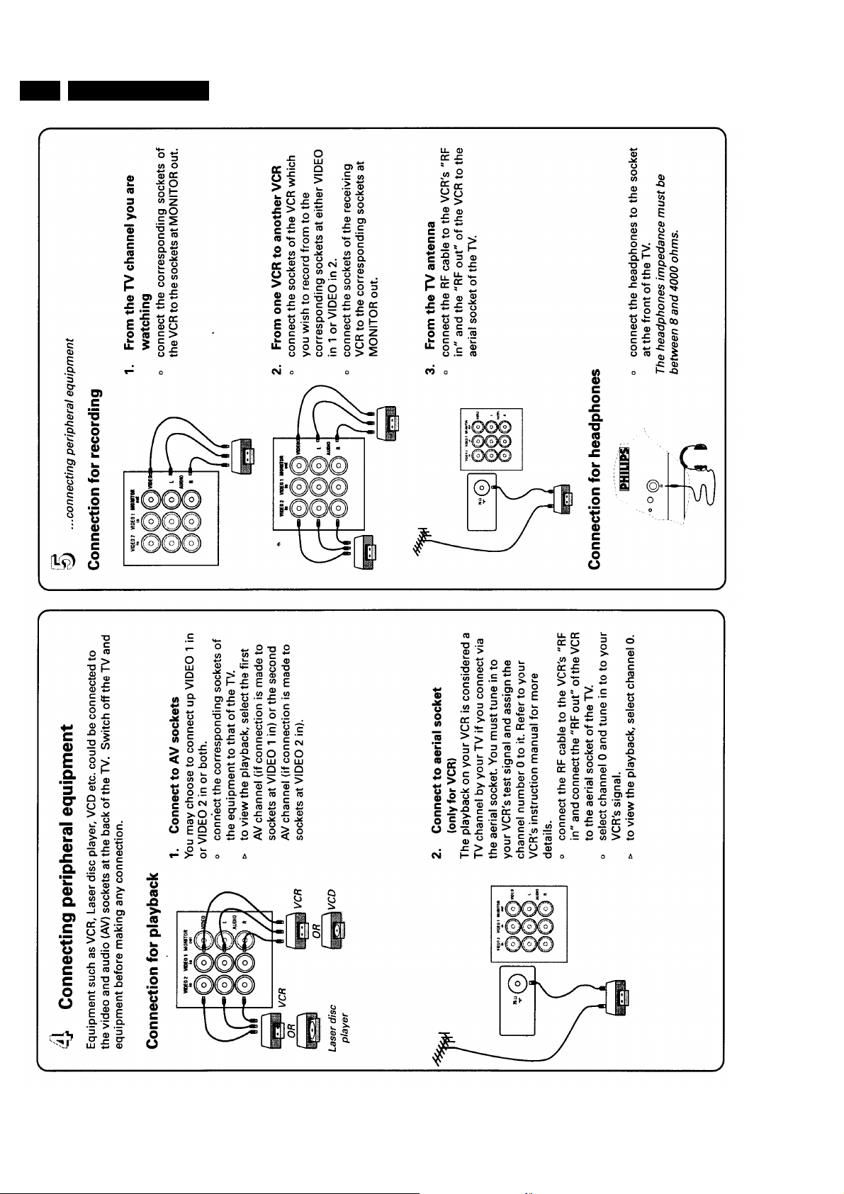
52 L9.1A
10 Directions for use
10 Directions for use
Page 27
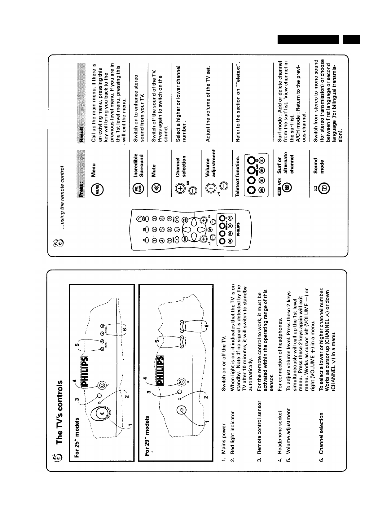
10 Directions for use
53L9.1A
Page 28
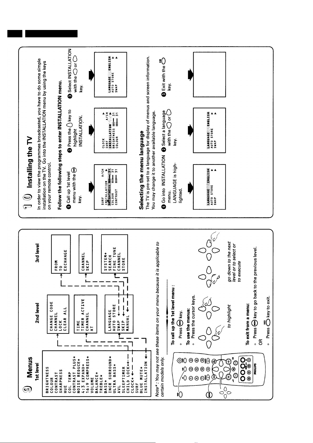
54 L9.1A
10 Directions for use
Page 29
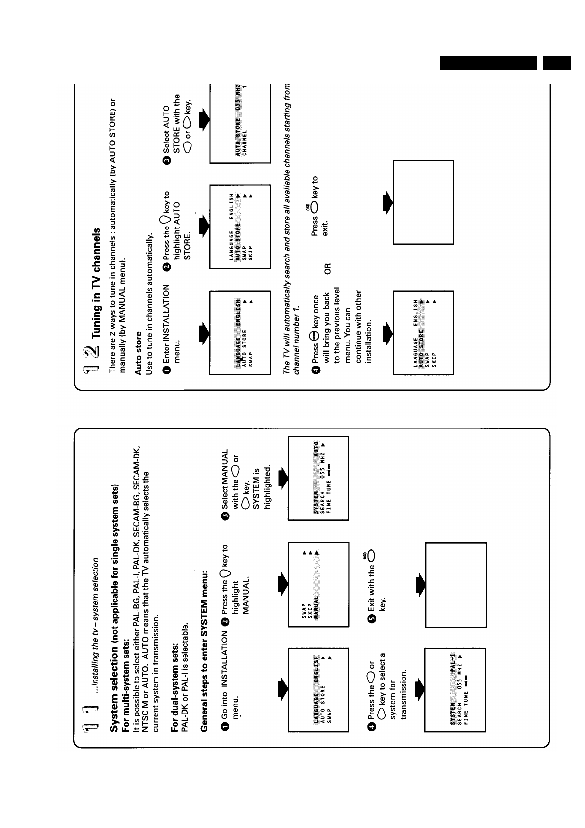
10 Directions for use
55L9.1A
Page 30
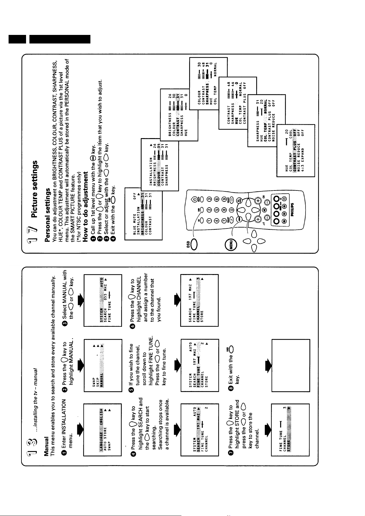
56 L9.1A
10 Directions for use
Page 31
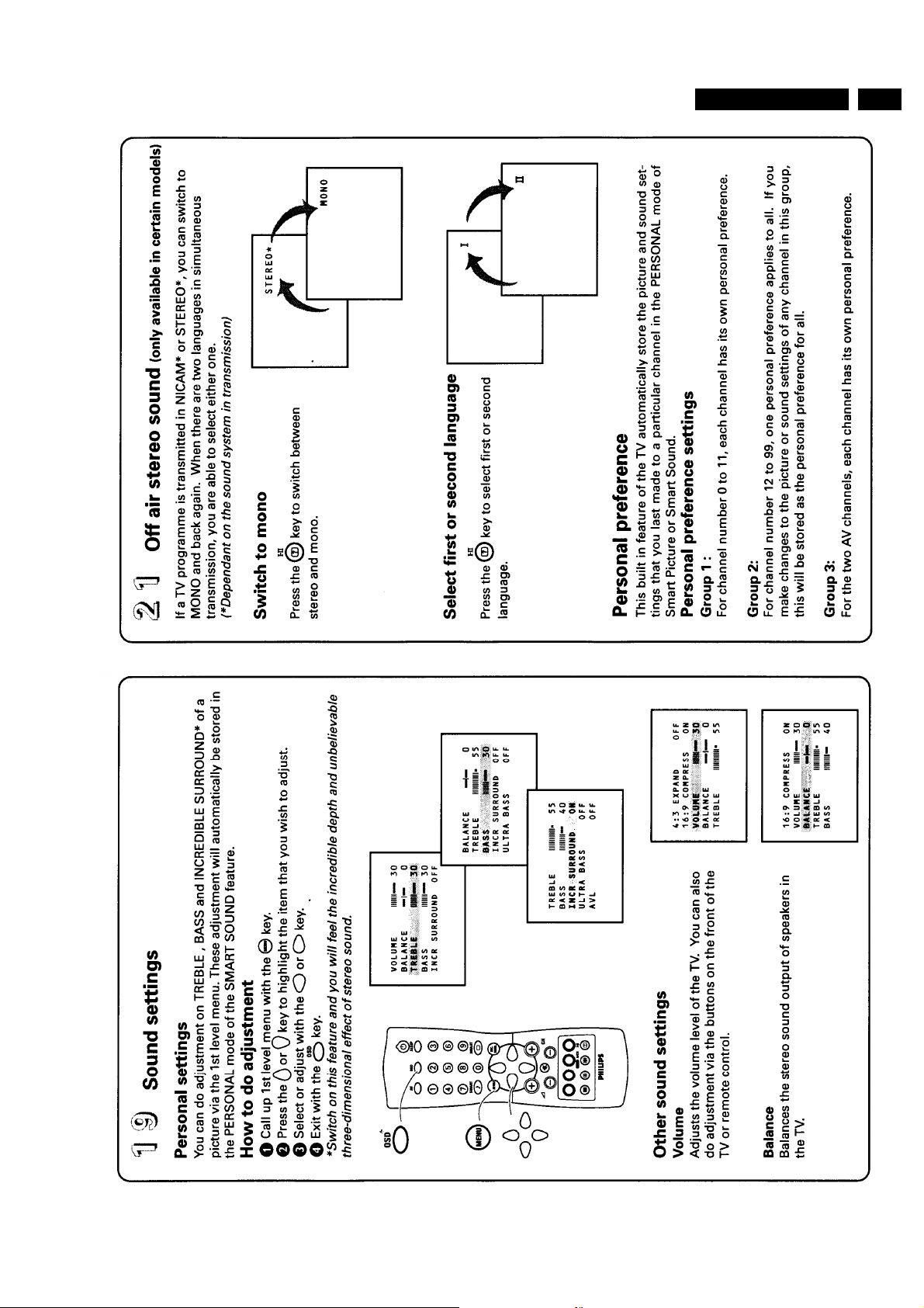
10 Directions for use
57L9.1A
Page 32
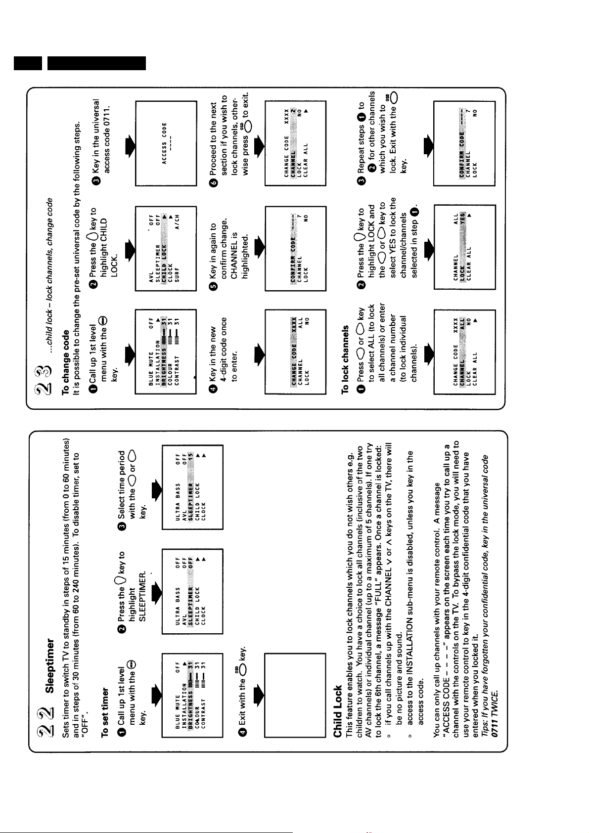
58 L9.1A
10 Directions for use
Page 33
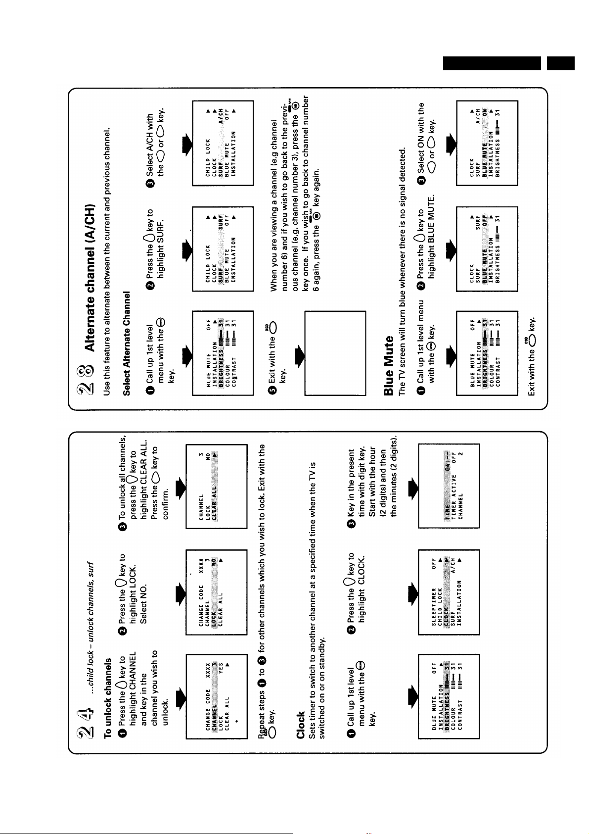
10 Directions for use
59L9.1A
Page 34
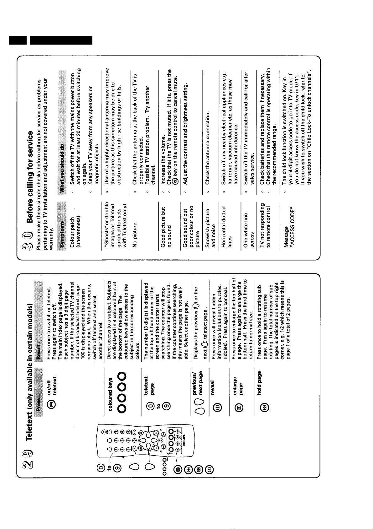
60 L9.1A
10 Directions for use
Page 35

11 List of Abbreviations
11 List of Abbreviations
2CS 2 Carrier Stereo A/P AsiaPacific; schematic/PCB information (only)
applicable for Asia Pacific sets
AFC Automatic Frequency Control
AQUADAG Aquadagcoatingonthe(outsideofthe)picture
tube
AudioOutR Audio signal at Right output channel.
AudioOutL/Mono Audio signal at Left output channel / Mono
output channel.
AV_MUTE Signal to mute the sound on the Audio-out of
Cinch / Scart (Combined with RBG_Blanking)
Ext2Fun_SW
(AV_Mute/
Ext2Fun_SW) Switching signal from Scart2 to micro
controller indicating the presence and type of
signal on Scart2. (no signal / CVBS 16:9 /
CVBS 4:3)
AV Audio Video signal
AVL Automatic Volume Level
B_TXT_OSD Blue TXT or OSD signal from uC to the video
controller IC7250 (BIMOS)
BASS Control signal for BASS
BCI Beam Current information
BTSC Broadcast Television Standard Committee;
sound standard for America and Asia Pacific
Buzzer Buzzer (only used in L9-ITV)
CRT DISCHARGE Fast drop of VBATT during after switch off the
set. Which result in EHT voltage reducing to
less than 18 kv within 5 sec.
CTI Colour Transient Improvement
CVBS ColourVideo BlankingSynchronisation. Video
signal containing colour, black/white, blanking
and synchronisation information.
CVBS_EXT CVBS external = CVBS signal form external
source (VCR, DVD etc.)
CVBS_INT CVBS internal = CVBS signal from the tuner
CVBS_MON CVBS monitor (CVBS) signal to Cinch or Scart
CVBS_Terr CVBS Terrestrial output signal
CVBS_TXT CVBS for TXT processing in micro controller
Din Digital input signal only used in L9-ITV)
Dout Digital output signal (only used in L9-ITV)
DBX Dynamic Bass Expander (only used for BTSC
sound system)
DNR Dynamic Noise Reduction
EAR Earth (ground layer)
EEPROM Electrically Erasable Programmable Read
Only Memory (also called NVM; non-volatile
memory)
EHT-INFO Extra high tension information; Beam current
related signal from CRT to BIMOS.
Ext1 B RGB External 1 Blue input signal.
Ext1 FB RGB External 1 Fast-blanking input signal.
Ext1 G RGB External 1 Green input signal.
Ext1 R RGB External 1 Red input signal.
Ext1 Video RGB External 1 Video input signal.
Ext2 AudioL/Mono External 2 Audio Left input signal / Mono input
signal.
Ext Audio/Mono ExternalAudio input signal/ Mono input signal.
Ext2 AudioR External 2 Audio Right input signal.
Ext2C Exterial2 SVHS Chrominance (C) input signal.
Ext2Video/Y External 2 Video input signal or SVHS
Luminance (Y) input signal.
ESD Electrostatic Discharge
EURO Europe; schematic/PCB information (only)
applicable for European sets
EWD_dyn Dynamic East-West correction to compensate
for variations in EHT
EWDRIVE East-West drive correction
FB_TXT_OSD Fast blanking signal from micro controller to
IC7250 (BIMOS) for inserting or displaying
TXT and OSD information (generated by the
micro processor) Filament Filament (heater voltage) from LOT to CRT
61L9.1A
FBL Fast Blanking
FFBL Full screen Fast Blanking
FM/AM/
Ext_VC_AudioMono FM, AM or external mono signal from BiMOS
to audio processor input (only used in Mono
and Nicam L sets)
Front/Ext1AudioL Front audio Left input signal / External 1 Audio
Left input signal.
Front/Ext1AudioR Front audio Right input signal / External 1
Audio Right input signal.
GND Ground
GND_LOT Ground of LOT
G_TXT_OSD Green TXT or OSD signal from micro
processor to the video controller IC7250
(BIMOS)
HD Horizontal pulse derivation
HDRIVE Horizontal output drive
HEW_protn Switching signal to (de)activate the XRAY
protection which is measured via pin 50 of the
BIMOS (only for USA sets)
Hflybk Horizontal flyback pulse used to monitor the
horizontal oscillator
IF Intermediate Frequency signal from the tuner
12C (or IIC) 2Wire communication protocol between micro
controller and integrated circuits
IC Integrated Circuit
I/O Input/Output
INT Audio internal output
IR Output signal from infrared receiver to micro
controller.
KeyBd1 Local keyboard control signal to micro
controller
KeyBd2 Local keyboard control signal to micro
controller (In protection mode KeyBd2 is
Ground)
KeyBd3 Local keyboard control signal to micro
controller
L- Power amplifier output to headphone and
speaker
L+ Power amplifier output to speaker
LED LEDcontrol signal from micro controllerto LED
LATAM Latin America; schematic/PCB information
(only) applicable for Latin American (incl.
Brazilian) sets
LeftOut Audio Left signal output
LTI Luminance Transient Improvement (=
steepness)
MainAudioL/Mono AudioLeft/Mono signal toinput power amplifier
MainAudioR Audio Right signal to input power amplifier
MON Audio monitor output
NICAM Near Instantaneous Companded Audio
Muliplex (digital audio)
NR Noise Reduction
NTSC NTSC colour system
OSD On Screen Display
P0Sys1/AM Switching signal with several functions:
BiMOS crystal selection (only for Latam
sets)Selection of AM or FM signal (used in
combination with P1Sys2/AMFM_ExtSel)
(only for Europe)
P1Sys2/
AMFM_ExtSel Switching signal with several functions:
BIMOS crystal selection (only for Latam
sets)Selection of internal AM/FM signal or an
external signal (used in combination with
P0Sys1/AM)
P2LLp/Mtrap Switchingsignal with severalfunctions: M-trap
(sound filtering) switching (only for A/P Pal
Multi sets)BiMOS crystal selection (only for
Latamsets)Selectionof L or L' system (only for
Europe sets)
P3Dual/Mono Switching signal to select the sound filter in
dual-system Mono sets (BG/I, BG/DK or I/DK).
Page 36

62 L9.1A
P4ScartPin8/SVHS Switching signal from I/O to micro controller
with several functions:Scart1 I/O: detects
signal type connected to Scart 1 (no signal,
16:9 signal, 4:3 signal) (only for Europe)Cinch
I/O: detects signal type connected to cinch:
SVHS or CVBS (not for Europe)
P5BassSw Bass switching signal (only for some mono
sets)
P6TrebleSw Treble switching signal (only for some mono
sets)
P7Ext1/2 Used in L9-ITV sets (Hotel TV)
P9stbyon+protn Signal from E-W and LOT output to micro
controller to (de)activate the protection mode
P10Mute/Volume Audio mute / Volume control signal pin
POR/CLK Power on reset (only used in L9-ITV sets)
R- Power amplifier output " R- " to speaker
R+ Power amplifier output " R+ " to headphone
and speaker
RAM Random Access Memory
RESET Reset signal to micro controller
RF_AGC Automatic gain control signal from BiMOS
output to tuner input.
RGB Red-Green-Blue
RGB_Blanking Red Green Blue Blanking signal (combined
with AV_MUTE)
RightOut Audio right signal output
R_TXT_OSD Red TXT or OSD signal from uC to the video
controller IC7250 (BIMOS)
ROM Read Only Memory
SAM Service Alignment Mode. Service mode for
alignments and error buffer display
SAP Second audio program (only for USA & A/P
sets)
SCL Clock line of the I2C-bus
SCL2 2nd Clock line of the IIC-bus (only used in L9-
ITV sets)
SDA Data line of the I2C-bus
SDA2 2nd Data line of the I2C-bus (only used in L9-
ITV sets)
SDM Service Default Mode. Service mode with
predefined settings for waveform and voltage
measurements, error buffer displayand option
(byte) setting.
SIF Sound IF signal for FM audio demodulator
SMPS Switching Mode Power Supply
STANDBY Switchingsignal from micro controller; "low" for
standby (power supply will be switched to
stand-by mode), "high" for normal operation
SW_OUT Selected Output signal from source
SYNC Synchronisation
TBD To Be Defined
TREBLE Control signal for treble
TXT Teletext
uC Micro controller
USA United States; schematic/PCB information
(only) applicable for North American sets
V_TUNE Tuning voltage for tuner
Vdrive - Negative Vertical drive pulse signal
Vdrive + Positive Vertical drive pulse signal
VD Vertical pulse derivation
VFL Verticalflyback pulse used to inform the micro
controller that flyback is occurring. This is
critical for the correct OSD and TXT
Vflybk Vertical flyback pulse
VG2 Voltage on grid 2 of the picture tube (screen
control)
VideoOut CVBS output signal
VOLUME Control signal (from micro controller, but on
DClevelvia RC network) for sound processing
in sound IC XRAY-PROT XRAY protection (only for USA sets) YC Luminance (Y) and Chrominance (C)
11 List of Abbreviations
Page 37

12 Spare parts list
63L9.1A
12 Spare parts list
Mono carrier [A]
Various
0127∆ 4822 256 92053 FUSE HOLDER
0151 4822 256 10336 LED HOLDER
0189∆ 4822 402 10844 PCB BRACKET
0211∆ 4822 265 20723 2P male (vert.)
0213∆ 4822 267 10775 2P MALE (Bl)
0224 4822 267 10676 Conn. 1P
0228 4822 267 10676 Conn. 1p
0231∆ 4822 276 14024 Mains switch
0232∆ 4822 267 31014 Headphone socket
0232∆ 4822 267 51391 F PHONE 3.5MM
0267 4822 267 31673 Headphone plug
1000∆ 4822 210 10852 Tuner TEDH9X007A
1000∆ 4822 210 10854 Tuner TEDH9X001A
1001 4822 242 10314 filter 5,5MHz
1003 4822 242 10357 filter 6,0MHz
1003 4822 242 10874 filter 47,5 MHz
1003 4822 242 81964 SAW filter
1200 4822 242 10315 cer. flt 5,5/5,7/
1200 4822 242 81712 cer. flt TPWA04B
1200 4822 242 81978 filter 4,5MHz
1201 4822 242 81572 filter 6,0MHz
1203 4822 242 81978 filter 4,5MHz
1206 4822 242 10705 cristal 3 583 056
1207 4822 242 10706 cristal 3 575 011
1208 4822 242 10776 cristal 3 579 545
1208 4822 242 81967 cristal 3 579 545
1500 4822 070 34002 Fuse (4A)
1572∆ 4822 071 51002 Fuse (1A)
1573∆ 4822 071 52502 Fuse (2.5A)
1580∆ 4822 280 10367 Relay
1600 4822 276 13775 SWITCH
1601 4822 276 13775 SWITCH
1602 4822 276 13775 SWITCH
1603 4822 276 13775 SWITCH
1660 4822 242 10694 cristal 12MHz
1822 4822 242 10769 cristal 18,432MHz
STEREO
OFWG1984M
6,5Mhz
MHz
MHz
MHz
MHz
g
2001 4822 126 13751 47nF 10% 63V
2002 4822 124 40255 100µF 20% 63V
2003 4822 124 40255 100µF 20% 63V
2004 5322 122 32654 22nF 10% 63V
2005 4822 122 33575 220pF 5% 63V
2006 4822 126 13695 82pF 1% 63V
2008 4822 122 33177 10nF 20% 50V
2009 5322 122 33861 120pF 10% 50V
2010 4822 122 33926 12pF 5% 50V
2011 4822 124 41579 10µF 20% 50V
2013 4822 126 10002 100nF 20% 25V
2014 4822 122 33177 10nF 20% 50V
2101 5322 122 31863 330pF 5% 63V
2102 5322 122 31863 330pF 5% 63V
2103 5322 122 31863 330pF 5% 63V
2104 5322 122 31863 330pF 5% 63V
2107 5322 122 31863 330pF 5% 63V
2109 5322 122 31863 330pF 5% 63V
2111 4822 124 41579 10µF 20% 50V
2112 4822 124 41579 10µF 20% 50V
2115 4822 126 13836 1µF 16V
2173 5322 122 31863 330pF 5% 63V
2174 4822 124 81029 100µF 20% 25V
2176 5322 122 31863 330pF 5% 63V
2177 4822 124 81029 100µF 20% 25V
2201 4822 124 40242 1µF 20% 63V
2202 5322 126 10465 3.9nF 10% 50V
2203 4822 124 41579 10µF 20% 50V
2204 5322 122 32531 100pF 5% 50V
2205 4822 122 33177 10nF 20% 50V
2205 4822 126 10002 100nF 20% 25V
2206 4822 126 10002 100nF 20% 25V
2207 4822 124 81029 100µF 20% 25V
2208 4822 124 81029 100µF 20% 25V
2209 4822 126 13482 470nF 20% 16V
2211 4822 126 13482 470nF 20% 16V
2212 4822 126 13482 470nF 20% 16V
2213 4822 126 13482 470nF 20% 16V
2214 5322 122 32654 22nF 10% 63V
2215 4822 124 41576 2.2µF 20% 50V
2216 4822 126 13561 220nF 10% 16V
2217 4822 122 33575 220pF 5% 63V
2217 4822 126 13689 18pF 1% 63V
2218 4822 126 13486 15pF 2% 63V
2219 4822 126 13486 15pF 2% 63V
2220 4822 122 33575 220pF 5% 63V
2220 4822 126 13486 15pF 2% 63V
2221 5322 126 10511 1nF 5% 50V
2222 4822 126 10002 100nF 20% 25V
2225 4822 126 13061 220nF 20% 25V
2226 4822 124 23489 33µF 20% 25V
2227 4822 124 40242 1µF 20% 63V
2247 4822 126 13751 47nF 10% 63V
2248 4822 126 13751 47nF 10% 63V
2249 4822 126 13751 47nF 10% 63V
2401 5322 121 42386 100nF 5% 63V
2402 5322 121 42386 100nF 5% 63V
2403 4822 124 40255 100µF 20% 63V
2404 4822 121 42408 220nF 5% 63V
2405 5322 122 32268 470pF 10% 50V
2407 5322 122 32268 470pF 10% 50V
2409 4822 121 42408 220nF 5% 63V
2420 5322 126 10223 4.7nF 10% 63V
2426 5322 121 42386 100nF 5% 63V
2428 4822 122 33175 2.2nF 20% 50V
2429 4822 124 40242 1µF 20% 63V
2430 4822 124 41579 10µF 20% 50V
2431 4822 126 10002 100nF 20% 25V
2437 4822 126 13061 220nF 20% 25V
2438 4822 126 13836 1µF 16V
2440 5322 126 10511 1nF 5% 50V
2441 5322 126 10511 1nF 5% 50V
2448 4822 122 31173 220pF 10% 500V
2450 4822 124 11575 47µF 20% 160V
2451 4822 121 41935 12nF 5% 250V
2451 4822 121 51305 15nF 10% 50V
2456 4822 121 43526 47nF 5% 250V
2457∆ 4822 121 10518 390nF 5% 250V
2457∆ 4822 121 43888 360nF 5% 250V
2458 4822 124 42127 10µF 20% 100V
2459 4822 126 13185 680pF 10% 500V
2461 4822 122 31175 1nF 10% 500V
2462 4822 121 43526 47nF 5% 250V
2463∆ 4822 126 14053 1nF 10% 2KV
2463∆ 4822 126 14138 680pF 10% 2KV
2463∆ 4822 126 14184 820pF 10% 2KV
2464 4822 121 10739 2.2µF 5% 160V
2465∆ 4822 121 70617 10nF 5% 1.6KV
2465∆ 4822 121 70649 9.1nF 5% 1.6KV
2466 4822 121 40483 10nF 10% 400V
2467∆ 4822 121 40488 22nF 10% 400V
2468∆ 4822 121 40488 22nF 10% 400V
2468 5322 121 44151 33nF 10% 400V
2469 4822 121 51319 1µF 10% 63V
2470 4822 122 31177 470pF 10% 500V
2471 4822 121 51252 470nF 5% 63V
2472 5322 124 41379 2.2µF 20% 50V
2473 4822 124 41751 47µF 20% 50V
2475 4822 126 14096 560nF 5% 250V
2481 4822 121 51252 470nF 5% 63V
2482 4822 121 40482 68nF 10% 250V
2484 5322 121 42386 100nF 5% 63V
2485 4822 124 81107 4.7µF 20% 250V
2486 4822 124 80791 470µF 20% 16V
2487 4822 124 40255 100µF 20% 63V
2488 4822 124 80791 470µF 20% 16V
2489 4822 124 80791 470µF 20% 16V
2490 4822 122 31177 470pF 10% 500V
2491 4822 122 31177 470pF 10% 500V
2492 4822 126 10326 180pF 5% 63V
2500∆ 4822 126 13589 470nF 275V
2501 4822 121 70141 33nF 5% 400V
2502∆ 4822 126 14153 2.2nF 10% 1KV
2504∆ 4822 126 14153 2.2nF 10% 1KV
2505∆ 4822 126 14153 2.2nF 10% 1KV
2507∆ 4822 126 11524 1.5nF 10% 1KV
2508 4822 124 12415 220µF 20% 400V
2508 4822 124 12442 330µF 20% 450V
2508∆ 4822 124 42159 330µF 20% 400V
2511∆ 4822 122 50116 470pF 10% 1KV
2517 5322 122 32331 1nF 10% 100V
2518∆ 4822 122 50116 470pF 10% 1KV
2520 4822 126 13695 82pF 1% 63V
2521 4822 122 33891 3.3nF 10% 63V
2522 4822 122 33891 3.3nF 10% 63V
2524 5322 122 31863 330pF 5% 63V
2529 4822 126 10002 100nF 20% 25V
2530 4822 124 11571 1µF 20% 50V
2531 4822 121 10738 1nF 2% 50V
2532 5322 122 32268 470pF 10% 50V
2533 4822 122 33175 2.2nF 20% 50V
2540 4822 124 80059 100µF 20% 25V
2541 4822 124 12416 3.3µF 20% 160V
2542 4822 124 40433 47µF 20% 25V
2545∆ 4822 126 14049 1.5nF 20% 250V
2550∆ 4822 122 50116 470pF 10% 1KV
2551 4822 124 42336 47µF 20% 160V
2561 4822 124 40784 3300µF 20% 16V
2562∆ 4822 126 13337 220pF 10% 1KV
2564 5322 122 34123 1nF 10% 50V
2565 5322 122 34123 1nF 10% 50V
2571 4822 124 12417 2200µF 20% 25V
2573 4822 126 12105 33nF 5% 50V
2575 4822 126 10002 100nF 20% 25V
2576 5322 122 31866 6.8nF 10% 63V
2586 4822 124 22263 220µF 20% 25V
2604 4822 124 81151 22µF 50V
2609 5322 126 10511 1nF 5% 50V
2613 5322 121 42386 100nF 5% 63V
2615 4822 126 10002 100nF 20% 25V
2616 5322 122 32658 22pF 5% 50V
2617 5322 122 32658 22pF 5% 50V
2618 5322 122 32531 100pF 5% 50V
2619 4822 124 40242 1µF 20% 63V
2620 5322 122 32658 22pF 5% 50V
2621 5322 122 32658 22pF 5% 50V
2622 4822 124 22263 220µF 20% 25V
2623 4822 122 33177 10nF 20% 50V
2624 4822 126 13694 68pF 1% 63V
2625 4822 122 33172 390pF 5% 50V
2626 4822 122 33172 390pF 5% 50V
2627 4822 122 33172 390pF 5% 50V
2628 4822 122 33172 390pF 5% 50V
2629 4822 122 30103 22nF 20% 63V
2630 4822 126 10002 100nF 20% 25V
2631 4822 126 13836 1µF 16V
2633 4822 122 33177 10nF 20% 50V
2679 4822 126 10002 100nF 20% 25V
2681 4822 124 22263 220µF 20% 25V
2697 5322 126 10511 1nF 5% 50V
2843 4822 124 81029 100µF 20% 25V
2850 4822 126 10326 180pF 5% 63V
2850 4822 126 13693 56pF 1% 63V
2851 5322 126 10511 1nF 5% 50V
2852 5322 126 10511 1nF 5% 50V
2853 5322 126 10511 1nF 5% 50V
2854 5322 126 10511 1nF 5% 50V
2855 5322 122 32286 3.3pF 5% 50V
2856 5322 122 32286 3.3pF 5% 50V
2857 4822 126 13836 1µF 16V
2858 4822 126 13692 47pF 1% 63V
2859 4822 126 13486 15pF 2% 63V
2860 4822 124 41579 10µF 20% 50V
2861 4822 126 10002 100nF 20% 25V
2862 4822 126 10002 100nF 20% 25V
2863 4822 124 41579 10µF 20% 50V
2864 4822 126 13061 220nF 20% 25V
2865 4822 126 13061 220nF 20% 25V
2866 4822 126 13061 220nF 20% 25V
2867 4822 126 13061 220nF 20% 25V
2868 4822 124 40769 4.7µF 20% 100V
2869 4822 126 10002 100nF 20% 25V
2870 4822 126 10002 100nF 20% 25V
2871 4822 124 41579 10µF 20% 50V
2874 4822 126 13692 47pF 1% 63V
2875 4822 126 13692 47pF 1% 63V
2877 4822 126 10002 100nF 20% 25V
2882 5322 126 10511 1nF 5% 50V
2883 4822 124 41579 10µF 20% 50V
2884 5322 126 10511 1nF 5% 50V
2887 4822 122 33575 220pF 5% 63V
2887 4822 126 10326 180pF 5% 63V
2888 4822 124 81029 100µF 20% 25V
2889 4822 126 10002 100nF 20% 25V
2891 4822 126 13691 27pF 1% 63V
2891 5322 122 32659 33pF 5% 50V
2950 4822 124 81029 100µF 20% 25V
2952 4822 126 13836 1µF 16V
2954 4822 126 13482 470nF 20% 16V
2955 4822 122 33177 10nF 20% 50V
2956 4822 126 13836 1µF 16V
2958 4822 126 13482 470nF 20% 16V
2959 4822 122 33177 10nF 20% 50V
2960 4822 124 11908 2200µF 20% 25V
2961 4822 124 11947 10µF 20% 16V
2962 5322 122 32448 10pF 5% 63V
2963 5322 122 32448 10pF 5% 63V
f
3000 4822 116 52175 100Ω 5% 0.5W 3001 4822 116 52175 100Ω 5% 0.5W 3010 4822 116 52228 680Ω 5% 0.5W 3013∆ 4822 051 20008 jumper (0805) 3014∆ 4822 051 20472 4k7 5% 0.1W 3015 4822 051 20223 22k 5% 0.1W 3016 4822 116 52228 680Ω 5% 0.5W 3021 4822 051 10102 1k 2% 0.25W 3023 4822 116 52243 1k5 5% 0.5W 3024 4822 116 52257 22k 5% 0.5W 3026 4822 051 20562 5k6 5% 0.1W 3100 4822 116 83868 150Ω 5% 0.5W 3101 4822 117 13579 220k 1% 0.1W 3103 4822 116 52303 8k2 5% 0.5W 3104 4822 117 10833 10k 1% 0.1W 3105 4822 116 83868 150Ω 5% 0.5W 3108 4822 116 52303 8k2 5% 0.5W 3109 4822 117 10833 10k 1% 0.1W 3122 4822 117 13579 220k 1% 0.1W 3123 4822 051 20759 75Ω 5% 0.1W 3125 4822 116 52199 68Ω 5% 0.5W 3131 4822 116 52303 8k2 5% 0.5W 3132 4822 117 10833 10k 1% 0.1W 3134 4822 116 52195 47Ω 5% 0.5W 3136 4822 116 52303 8k2 5% 0.5W 3137 4822 117 10833 10k 1% 0.1W 3140 4822 116 52201 75Ω 5% 0.5W 3141 4822 116 52175 100Ω 5% 0.5W 3142 4822 116 52201 75Ω 5% 0.5W 3155∆ 4822 051 20471 470Ω 5% 0.1W 3156 4822 116 52206 120Ω 5% 0.5W 3157 4822 116 52206 120Ω 5% 0.5W 3161 4822 117 10834 47k 1% 0.1W 3162 4822 117 10834 47k 1% 0.1W 3200 4822 051 20561 560Ω 5% 0.1W 3201 4822 051 20182 1k8 5% 0.1W 3201 4822 051 20391 390Ω 5% 0.1W 3203 4822 051 20331 330Ω 5% 0.1W
3204 4822 116 52249 1k8 5% 0.5W 3205 4822 051 10102 1k 2% 0.25W 3206 4822 051 20561 560Ω 5% 0.1W 3206 4822 117 10353 150Ω 1% 0.1W 3208 4822 116 52175 100Ω 5% 0.5W 3209 4822 051 20223 22k 5% 0.1W 3210∆ 4822 051 20472 4k7 5% 0.1W 3211∆ 4822 051 20472 4k7 5% 0.1W 3212 4822 051 20391 390Ω 5% 0.1W 3213 4822 051 20561 560Ω 5% 0.1W 3215 4822 051 20223 22k 5% 0.1W 3216∆ 4822 051 20008 jumper (0805) 3216 4822 117 10353 150Ω 1% 0.1W 3218∆ 4822 051 20101 100Ω 5% 0.1W 3219 4822 051 20561 560Ω 5% 0.1W 3220∆ 4822 051 20101 100Ω 5% 0.1W 3222 4822 116 52303 8k2 5% 0.5W 3223 4822 116 52303 8k2 5% 0.5W 3224 4822 116 52303 8k2 5% 0.5W 3225 4822 051 20104 100k 5% 0.1W 3228∆ 4822 051 20101 100Ω 5% 0.1W 3243∆ 4822 051 20472 4k7 5% 0.1W 3246 4822 117 11149 82k 1% 0.1W 3247 4822 116 52175 100Ω 5% 0.5W 3248 4822 116 52175 100Ω 5% 0.5W 3249 4822 051 20334 330k 5% 0.1W 3250∆ 4822 051 20008 jumper (0805) 3251 4822 051 20104 100k 5% 0.1W 3251 4822 051 20274 270k 5% 0.1W 3251 4822 051 20474 470k 5% 0.1W 3251 4822 051 20684 680k 5% 0.1W 3252 4822 117 11449 2k2 1% 0.1W 3253 4822 117 11449 2k2 1% 0.1W 3257∆ 4822 051 20101 100Ω 5% 0.1W 3258∆ 4822 051 20101 100Ω 5% 0.1W 3259∆ 4822 051 20101 100Ω 5% 0.1W 3265 4822 051 20104 100k 5% 0.1W 3401 4822 111 31051 3Ω3 5% 3402 4822 111 31051 3Ω3 5% 3403 4822 111 31051 3Ω3 5% 3405 4822 050 22002 2k 1% 0.6W 3405 4822 050 22202 2k2 1% 0.6W 3406 4822 050 11002 1k 1% 0.4W 3407 4822 050 22002 2k 1% 0.6W 3407 4822 050 22202 2k2 1% 0.6W 3408 4822 050 11002 1k 1% 0.4W 3409∆ 4822 052 10158 1Ω5 5% 0.33W 3410 4822 116 83872 220Ω 5% 0.5W 3411 4822 116 83872 220Ω 5% 0.5W 3420 4822 051 20474 470k 5% 0.1W 3421 4822 116 52256 2k2 5% 0.5W 3422 4822 116 52256 2k2 5% 0.5W 3423 4822 051 20684 680k 5% 0.1W 3424 4822 051 20106 10M 5% 0.1W 3425 4822 051 20124 120k 5% 0.1W 3425 4822 051 20154 150k 5% 0.1W 3425 4822 117 11148 56k 1% 0.1W 3426 4822 051 20393 39k 5% 0.1W 3428 4822 051 20223 22k 5% 0.1W 3429 4822 051 20273 27k 5% 0.1W 3431∆ 4822 051 20332 3k3 5% 0.1W 3432∆ 4822 051 20101 100Ω 5% 0.1W 3436 4822 051 10102 1k 2% 0.25W 3437 4822 117 10833 10k 1% 0.1W 3438 4822 116 52271 33k 5% 0.5W 3442 4822 116 52276 3k9 5% 0.5W 3448 4822 116 52303 8k2 5% 0.5W 3449 4822 116 52269 3k3 5% 0.5W 3452 4822 053 12229 22Ω 5% 3W 3452∆ 4822 053 12339 33Ω 5% 3W 3453 4822 117 12822 4Ω7 5% 5W 3454 4822 053 11333 33k 5% 2W 3458 4822 050 11002 1k 1% 0.4W 3461 4822 116 52283 4k7 5% 0.5W 3462 4822 117 12514 6k8 5% 5W 3463 4822 116 52195 47Ω 5% 0.5W 3465∆ 4822 052 10109 10Ω 5% 0.33W 3468 4822 050 11002 1k 1% 0.4W 3470 4822 116 52271 33k 5% 0.5W 3471 4822 116 83874 220k 5% 0.5W 3472 4822 116 52234 100k 5% 0.5W 3472 4822 116 52304 82k 5% 0.5W 3473 4822 050 11002 1k 1% 0.4W 3474 4822 050 24708 4Ω7 1% 0.6W 3474 4822 111 31051 3Ω3 5% 3475 4822 050 24708 4Ω7 1% 0.6W 3475 4822 111 31051 3Ω3 5% 3477 4822 116 52175 100Ω 5% 0.5W 3478 4822 116 83874 220k 5% 0.5W 3479 4822 116 52219 330Ω 5% 0.5W 3480 4822 050 22703 27k 1% 0.6W 3481 4822 050 21004 100k 1% 0.6W 3481 4822 050 22703 27k 1% 0.6W 3481 4822 117 13667 32k4 1% 0.5W 3481 4822 117 13672 35k7 1% 0.6W 3482∆ 4822 050 24703 47k 1% 0.6W 3482 4822 050 25603 56k 1% 0.6W 3483 4822 116 52257 22k 5% 0.5W 3484 4822 116 83864 10k 5% 0.5W 3485∆ 4822 052 11478 4Ω7 5% 0.5W 3486 4822 052 11108 1Ω 5% 0.5W 3487 4822 052 11108 1Ω 5% 0.5W 3488∆ 4822 052 11478 4Ω7 5% 0.5W 3490 4822 052 11108 1Ω 5% 0.5W
Page 38
64 L9.1A
12 Spare parts list
3491 4822 052 11108 1Ω 5% 0.5W
3492 4822 052 11108 1Ω 5% 0.5W
3495 4822 117 11507 6k8 1% 0.1W
3496 4822 117 10833 10k 1% 0.1W
3497 4822 117 10833 10k 1% 0.1W
3501 4822 117 12181 470Ω 20% 0.5W
3502∆ 4822 053 21225 2M2 5% 0.5W
3503 4822 116 10105 9Ω 220V PTC
3505∆ 4822 252 11215 Surge prot.
3507 4822 116 82776 2Ω2
3508 4822 117 13473 22k 5% 2.5W PR03
3510∆ 4822 116 82107 68k 5% 3W
3510 4822 117 11488 33k 5% 3W
3511 4822 117 12568 1k 10% 7W
3512∆ 4822 051 20153 15k 5% 0.1W
3513 4822 117 11719 180k
3514 4822 050 28204 820k 1% 0.6W
3515 4822 116 30451 NTC
3516 4822 051 10102 1k 2% 0.25W
3517 4822 050 11002 1k 1% 0.4W
3518∆ 4822 116 83027 R22 5% 3W
3520 4822 116 52304 82k 5% 0.5W
3521 4822 051 20331 330Ω 5% 0.1W
3525∆ 4822 052 10339 33Ω 5% 0.33W
3528 4822 116 52175 100Ω 5% 0.5W
3529 4822 116 52199 68Ω 5% 0.5W
3530 4822 116 52269 3k3 5% 0.5W
3532 4822 116 83961 6k8 5%
3534∆ 4822 051 20153 15k 5% 0.1W
3536 4822 116 52251 18k 5% 0.5W
3537 4822 116 83864 10k 5% 0.5W
3542∆ 4822 053 21475 4M7 5% 0.5W
3543 4822 116 83874 220k 5% 0.5W
3544 4822 051 20273 27k 5% 0.1W
3545 4822 116 52271 33k 5% 0.5W
3546 4822 117 10834 47k 1% 0.1W
3547 4822 051 10102 1k 2% 0.25W
3570∆ 4822 051 20153 15k 5% 0.1W
3570 4822 117 10833 10k 1% 0.1W
3571 4822 050 21504 150k 1% 0.6W
3571 4822 050 21604 160k 1% 0.6W
3573 4822 117 11951 2k 1% 0.1W
3574 4822 051 20333 33k 5% 0.1W
3575 4822 116 52175 100Ω 5% 0.5W
3577 4822 116 83864 10k 5% 0.5W
3578 4822 051 10102 1k 2% 0.25W
3579 5322 117 12487 1k 1% 0.125W
3585 4822 116 52175 100Ω 5% 0.5W
3592 4822 117 10833 10k 1% 0.1W
3594 4822 051 20223 22k 5% 0.1W
3595 4822 116 52297 68k 5% 0.5W
3596 4822 116 83864 10k 5% 0.5W
3597∆ 4822 051 20101 100Ω 5% 0.1W
3598 4822 117 10833 10k 1% 0.1W
3599 4822 051 20223 22k 5% 0.1W
3607 4822 116 90884 8k2 x10
3608 4822 117 12168 2k2 x6
3609 4822 117 13649 2k2 5% 7X
3611 4822 051 10102 1k 2% 0.25W
3612 4822 117 10833 10k 1% 0.1W
3613 4822 117 10833 10k 1% 0.1W
3617 4822 051 20822 8k2 5% 0.1W
3618 4822 116 52175 100Ω 5% 0.5W
3619∆ 4822 051 20472 4k7 5% 0.1W
3629∆ 4822 051 20471 470Ω 5% 0.1W
3630 4822 116 83883 470Ω 5% 0.5W
3631 4822 051 20273 27k 5% 0.1W
3632 4822 053 12479 47Ω 5% 3W
3633 4822 116 52231 820Ω 5% 0.5W
3634 4822 117 11449 2k2 1% 0.1W
3635 4822 051 20223 22k 5% 0.1W
3636 4822 051 20223 22k 5% 0.1W
3651 4822 116 52175 100Ω 5% 0.5W
3652 4822 116 52175 100Ω 5% 0.5W
3653 4822 116 83864 10k 5% 0.5W
3654∆ 4822 051 20101 100Ω 5% 0.1W
3655∆ 4822 051 20101 100Ω 5% 0.1W
3657 4822 116 83876 270Ω 5% 0.5W
3661 4822 116 52175 100Ω 5% 0.5W
3662∆ 4822 051 20472 4k7 5% 0.1W
3663 4822 051 20822 8k2 5% 0.1W
3664 4822 051 20822 8k2 5% 0.1W
3665∆ 4822 051 20472 4k7 5% 0.1W
3666 4822 051 20562 5k6 5% 0.1W
3667 4822 051 20273 27k 5% 0.1W
3672∆ 4822 051 20472 4k7 5% 0.1W
3673 4822 117 10833 10k 1% 0.1W
3674 4822 051 20182 1k8 5% 0.1W
3675 4822 117 10353 150Ω 1% 0.1W
3676 4822 117 10353 150Ω 1% 0.1W
3677 4822 117 10353 150Ω 1% 0.1W
3680 4822 051 20681 680Ω 5% 0.1W
3681∆ 4822 051 20472 4k7 5% 0.1W
3682 4822 051 20822 8k2 5% 0.1W
3683∆ 4822 051 20101 100Ω 5% 0.1W
3684∆ 4822 051 20332 3k3 5% 0.1W
3686 4822 051 20822 8k2 5% 0.1W
3841 4822 116 52175 100Ω 5% 0.5W
3842 4822 116 52175 100Ω 5% 0.5W
3843 4822 117 10834 47k 1% 0.1W
3844∆ 4822 051 20471 470Ω 5% 0.1W
3845∆ 4822 051 20471 470Ω 5% 0.1W
3850 4822 117 11449 2k2 1% 0.1W
DSP301N-A21F
3950 4822 116 52228 680Ω 5% 0.5W 3951∆ 4822 051 20332 3k3 5% 0.1W 3952 4822 116 52175 100Ω 5% 0.5W 3953 4822 117 11507 6k8 1% 0.1W 3954 4822 117 11139 1k5 1% 0.1W 3955 4822 116 52283 4k7 5% 0.5W 3956 4822 117 11139 1k5 1% 0.1W 3957 4822 116 52283 4k7 5% 0.5W 4xxx 4822 051 10008 0Ω 5% 0.25W 4xxx 4822 051 20008 0Ω 5% 0.25W
b
5000 4822 157 51216 5.6µH
5002 4822 157 70439 Adj. coil
5004 4822 157 62411 0.82µH 20%
5101 4822 157 11867 5.6µH 5%
5201 4822 157 50961 22µH
5202 4822 157 11139 6.8µH 5%
5445∆ 4822 140 10666 LOT (pow. slot)29"
5445∆ 4822 140 10667 LOT 25"
5451 4822 157 11869 33µH 10%
5451 4822 157 71266 27µH
5457 4822 157 11671 lin. drum coil
5457 4822 157 11883 42µH 20%
5461∆ 4822 142 40351 LINE DRIVE TRAFO
5463 4822 157 11884 BRIDGE COIL
5465 4822 157 11886 BRIDGE COIL
5470 4822 157 11887 11000µH 15%
5471 4822 157 11885 1000µH 5%
5480 4822 156 20966 47 µH
5480 4822 157 70468 56µH
5480 4822 157 70698 27µH
5500∆ 4822 157 11523 5mH
5502 4822 157 10476 DMF-2820H
5502 4822 157 11538 10mH
5516 4822 157 60171 BEAD EMI 100MhZ
5518 4822 526 10704 100mH
5521 4822 157 62552 2.2µH
5540 4822 157 11835 4.7µH 5%
5545∆ 4822 146 11152 Transformer
5550 4822 157 60171 Bead EMI 100MHz
5551 4822 157 71401 27µH
5552 4822 526 10704 100mH
5572 4822 157 60171 Bead EMI 100MHz
5573 4822 157 60171 Bead EMI 100MHz
5575 4822 157 60171 Bead EMI 100MHz
5576 4822 157 60171 Bead EMI 100MHz
5577 4822 526 10704 100mH
5600 4822 157 62767 8.2µH
5601 4822 157 62767 8.2µH
5620 4822 157 11139 6.8µH 5%
5821 4822 157 50964 100µH
5831 4822 157 50943 12µH
5832 4822 157 50943 12µH
5833 4822 157 11743 12µH 5%
83R
83R
83R
83R
83R
83R
d
6007 5322 130 34955 BA482
6008 4822 130 34142 BZX79-B33
6113 4822 130 10852 BZX284-C6V8
6122 4822 130 10852 BZX284-C6V8
6124 4822 130 10852 BZX284-C6V8
6125 4822 130 10852 BZX284-C6V8
6211 4822 130 30621 1N4148
6212 4822 130 30621 1N4148
6213 4822 130 30621 1N4148
6401 4822 130 42488 BYD33D
6402 4822 130 31024 BZX79-B18
6402 4822 130 34142 BZX79-B33
6403 4822 130 42488 BYD33D
6404 4822 130 42488 BYD33D
6449 4822 130 30621 1N4148
6450 4822 130 30621 1N4148
6460 4822 130 41275 BY228
6461 4822 130 41602 BYW95C
6463 4822 130 30621 1N4148
6465 4822 130 42606 BYD33J
6466 4822 130 42606 BYD33J
6470 4822 130 30862 BZX79-B9V1
6471 4822 130 30621 1N4148
6472 4822 130 30621 1N4148
6473 4822 130 34145 BZX79-B39
6480 4822 130 34379 BZX79-B27
6481 4822 130 30621 1N4148
6485 4822 130 42606 BYD33J
6486 4822 130 10256 EGP20DL-5300
6487 4822 130 42488 BYD33D
6488 4822 130 10871 SBYV27-200
6490 4822 130 10871 SBYV27-200
6500 4822 130 34328 BZX79-B30
6501 4822 130 34328 BZX79-B30
6505 4822 130 10741 GBU6J
6505 4822 130 83794 GBU4K
6507 4822 130 42606 BYD33J
6508 4822 130 42606 BYD33J
6510 4822 130 34499 BZX79-B20
6511 4822 130 41487 BYV95C
6512 4822 130 31083 BYW55
6513 4822 130 31083 BYW55
6514 4822 130 31024 BZX79-B18
6540 4822 130 30842 BAV21
6542 4822 130 30842 BAV21
6543 4822 130 83757 BAS216
6550 4822 130 10218 BY229X-800
6560 4822 130 10256 EGP20DL-5300
6570 4822 130 10256 EGP20DL-5300
6582 4822 130 10256 EGP20DL-5300
6584 4822 130 30621 1N4148
6585 4822 130 30621 1N4148
6590 4822 130 10256 EGP20DL-5300
6591 4822 130 83757 BAS216
6601 4822 130 31981 BZX79-B3V9
6606 4822 130 34174 BZX79-B4V7
6607 4822 130 34278 BZX79-B6V8
6663 4822 130 82223 LTL307E
6831 4822 130 83757 BAS216
6951 4822 130 83757 BAS216
6961 4822 130 83757 BAS216
ce
7134 4822 130 40959 BC547B
7250 4822 209 17221 TDA8844/N2/S1
7250 4822 209 17464 TDA8843/N2/S1
7250 4822 209 17539 TDA8841/N2/S1
7250 4822 209 17543 TDA8847/N2/S1
7251∆ 4822 209 80591 LM317T
7252 5322 130 60508 BC857B
7253 5322 130 60508 BC857B
7254 4822 130 60511 BC847B
7256 4822 130 60511 BC847B
7257 5322 130 42718 BFS20
7258 4822 130 60511 BC847B
7259 5322 130 42718 BFS20
7261 5322 130 42718 BFS20
7263 5322 130 60508 BC857B
7266 4822 130 60511 BC847B
7401 4822 209 13176 TDA9302H
7401 4822 209 16352 STV9379FA
7460 4822 130 63569 BU1508DX
7461 4822 130 42159 BF819
7470 4822 130 11336 STP16NE06FP
7480 4822 209 90008 L78M05CP
7481 4822 130 44568 BC557B
7482 5322 130 60508 BC857B
7518 4822 130 63698 STH8NA60FI
7520 4822 209 15684 MC44603AP
7542 5322 130 60508 BC857B
7570 4822 209 81397 TL431CLPST
7581∆ 4822 209 71634 TCDT1101G
7590 4822 130 60511 BC847B
7591 4822 130 60511 BC847B
7592 4822 130 60511 BC847B
7600 4822 209 17537 SAA5563/M2A/0018
7600 4822 209 17538 SAA5542PS/M2A/
7600 4822 209 17542 SAA5543PS/M2A/
7601∆ 4822 209 15546 ST24W08B6
7601 4822 209 15822 ST24W04B6
7603∆ 4822 130 41344 BC337-40
7604 4822 130 60511 BC847B
7605 4822 130 60511 BC847B
7608 4822 130 60511 BC847B
7609 4822 130 60511 BC847B
7680 4822 218 12055 TSOP2836UH1
7833 4822 209 17461 MSP3415D-PP-A2
7833 4822 209 17544 MSP3435G-PP-A4
7833 4822 209 17545 BSP3505D-PP-A2
7950 4822 209 13646 TDA7057AQ/N2
0017
0019
CRT panel [B]
Various
0141 4822 492 70788 IC fixation
0254∆ 4822 267 20466 CON 9P fem
1013 4822 212 11999 CRT PANEL
g
2330 4822 121 51473 470nF 20% 63V
2340 4822 124 11565 10µF 20% 250V
2341 4822 126 13599 3.3nF 10% 500V
2343∆ 4822 126 12278 3300pF 10% 2KV
2345 4822 122 31175 1nF 10% 500V
f
3331 4822 116 52175 100Ω 5% 0.5W 3332 4822 117 11635 1k 10% 0.5W 3333 4822 116 52175 100Ω 5% 0.5W
3334 4822 117 11635 1k 10% 0.5W 3335 4822 116 52175 100Ω 5% 0.5W 3336 4822 117 11635 1k 10% 0.5W 3340∆ 4822 052 10109 10Ω 5% 0.33W 3341∆ 4822 052 10108 1Ω 5% 0.33W 3342∆ 4822 052 10108 1Ω 5% 0.33W 3343 4822 117 11896 1k5 20% 0.5W 3344 4822 116 52186 22Ω 5% 0.5W 3345 4822 117 13016 VDR 50-115V 3346 4822 116 52186 22Ω 5% 0.5W
b
5342 4822 157 50961 22µH
d
6331 4822 130 30842 BAV21
6333 4822 130 30842 BAV21
6335 4822 130 30842 BAV21
ce
7330∆ 4822 209 16321 TDA6107Q/N1
SIDE AV [E]
Various
0021∆ 4822 402 11334 SIDE AV BRACKET
0250 4822 265 11606 Conn. 3P
0251 4822 267 10735 Conn. 3P
0252 4822 267 10565 Conn. 4P
0253 4822 267 10735 Conn. 3P
1040 4822 212 11997 Side AV panel
g
2171 4822 126 13512 330pF 10% 50V
2172 4822 126 13512 330pF 10% 50V
f
3150 4822 116 83864 10k 5% 0.5W 3151 4822 116 52303 8k2 5% 0.5W 3152 4822 116 83864 10k 5% 0.5W 3153 4822 116 52303 8k2 5% 0.5W 3155 4822 116 52201 75Ω 5% 0.5W
d
6161 4822 130 34278 BZX79-B6V8
 Loading...